DC1472A-LTM4618EV Evaluation Kit Quick Start Guide
8
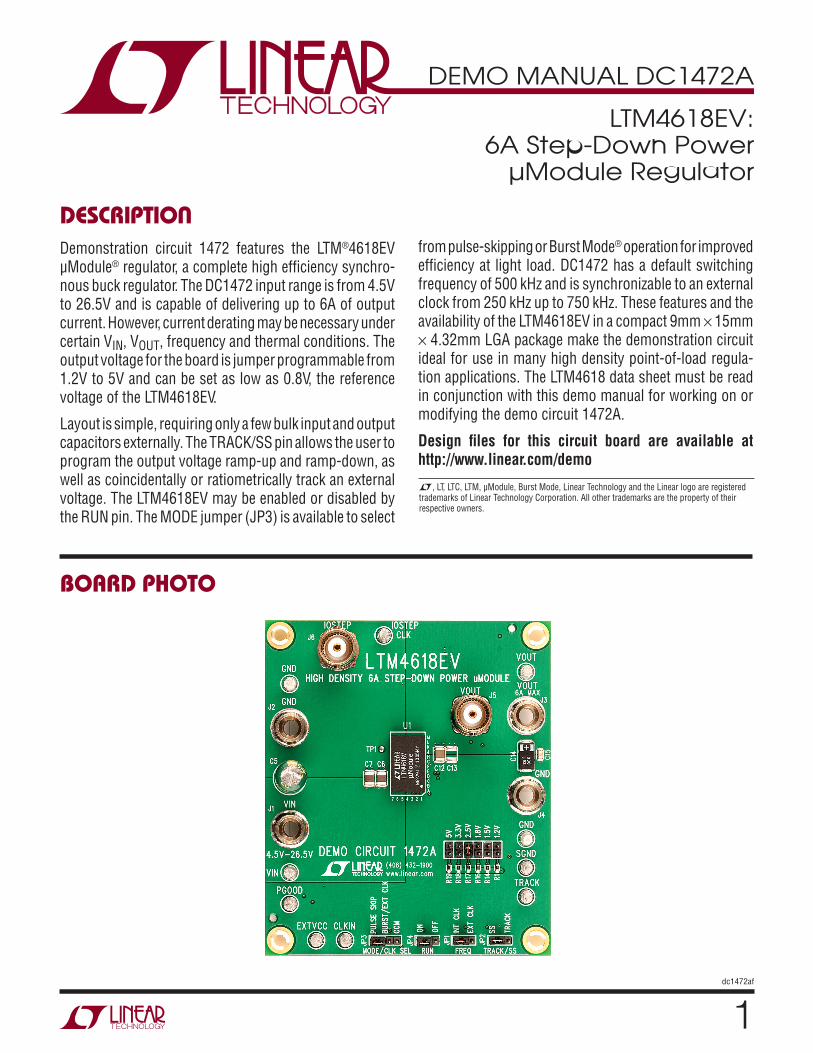
1 dc1472af DEMO MANUAL DC1472A DESCRIPTION LTM4618EV: 6A Step-Down Power μModule Regulator Demonstration circuit 1472 features the LTM ® 4618EV μModule ® regulator, a complete high efficiency synchro- nous buck regulator. The DC1472 input range is from 4.5V to 26.5V and is capable of delivering up to 6A of output current. However, current derating may be necessary under certain V IN , V OUT , frequency and thermal conditions. The output voltage for the board is jumper programmable from 1.2V to 5V and can be set as low as 0.8V, the reference voltage of the LTM4618EV. Layout is simple, requiring only a few bulk input and output capacitors externally. The TRACK/SS pin allows the user to program the output voltage ramp-up and ramp-down, as well as coincidentally or ratiometrically track an external voltage. The LTM4618EV may be enabled or disabled by the RUN pin. The MODE jumper (JP3) is available to select L, LT, LTC, LTM, μModule, Burst Mode, Linear Technology and the Linear logo are registered trademarks of Linear Technology Corporation. All other trademarks are the property of their respective owners. BOARD PHOTO from pulse-skipping or Burst Mode ® operation for improved efficiency at light load. DC1472 has a default switching frequency of 500 kHz and is synchronizable to an external clock from 250 kHz up to 750 kHz. These features and the availability of the LTM4618EV in a compact 9mm × 15mm × 4.32mm LGA package make the demonstration circuit ideal for use in many high density point-of-load regula- tion applications. The LTM4618 data sheet must be read in conjunction with this demo manual for working on or modifying the demo circuit 1472A. Design files for this circuit board are available at http://www.linear.com/demo
Transcript of DC1472A-LTM4618EV Evaluation Kit Quick Start Guide
1dc1472af
DEMO MANUAL DC1472A
DESCRIPTION
LTM4618EV: 6A Step-Down Power
µModule Regulator
Demonstration circuit 1472 features the LTM®4618EV μModule® regulator, a complete high effi ciency synchro-nous buck regulator. The DC1472 input range is from 4.5V to 26.5V and is capable of delivering up to 6A of output current. However, current derating may be necessary under certain VIN, VOUT, frequency and thermal conditions. The output voltage for the board is jumper programmable from 1.2V to 5V and can be set as low as 0.8V, the reference voltage of the LTM4618EV.
Layout is simple, requiring only a few bulk input and output capacitors externally. The TRACK/SS pin allows the user to program the output voltage ramp-up and ramp-down, as well as coincidentally or ratiometrically track an external voltage. The LTM4618EV may be enabled or disabled by the RUN pin. The MODE jumper (JP3) is available to select
L, LT, LTC, LTM, μModule, Burst Mode, Linear Technology and the Linear logo are registered trademarks of Linear Technology Corporation. All other trademarks are the property of their respective owners.
BOARD PHOTO
from pulse-skipping or Burst Mode® operation for improved effi ciency at light load. DC1472 has a default switching frequency of 500 kHz and is synchronizable to an external clock from 250 kHz up to 750 kHz. These features and the availability of the LTM4618EV in a compact 9mm × 15mm × 4.32mm LGA package make the demonstration circuit ideal for use in many high density point-of-load regula-tion applications. The LTM4618 data sheet must be read in conjunction with this demo manual for working on or modifying the demo circuit 1472A.
Design fi les for this circuit board are available at http://www.linear.com/demo
2dc1472af
DEMO MANUAL DC1472A
QUICK START PROCEDURE
PERFORMANCE SUMMARY
PARAMETER CONDITIONS/NOTES VALUE
Input Voltage Range 4.5V to 26.5V
Jumper Selectable Output Voltage, VOUT VIN = 4.5V – 26.5V, IOUT = 0A – 6A 1.2V, 1.5V, 1.8V, 2.5V, 3.3V or 5V ±2%
Maximum Continuous Output Current Derating is Necessary for Certain Operating Conditions. See Data Sheet for Details
6ADC
Default Operating Frequency R3 = 10kΩ, R4 = 3.16kΩ 500kHz
External Clock Sync. Frequency Range 250kHz to 750kHz
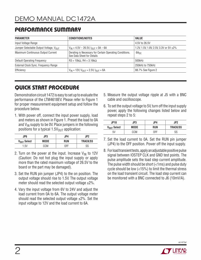
Effi ciency VIN = 12V, VOUT = 2.5V, IOUT = 6A 88.7% See Figure 2
Demonstration circuit 1472 is easy to set up to evaluate the performance of the LTM4618EV. Please refer to Figure 1 for proper measurement equipment setup and follow the procedure below.
1. With power off, connect the input power supply, load and meters as shown in Figure 1. Preset the load to 0A and VIN supply to be 0V. Place jumpers in the following positions for a typical 1.5VOUT application:
JP6 JP3 JP4 JP2
VOUT Select MODE RUN TRACK/SS
1.5V CCM OFF SS
2. Turn on the power at the input. Increase VIN to 12V (Caution: Do not hot plug the input supply or apply more than the rated maximum voltage of 26.5V to the board or the part may be damaged).
3. Set the RUN pin jumper (JP4) to the on position. The output voltage should rise to 1.5V. The output voltage meter should read the selected output voltage ±2%.
4. Vary the input voltage from 6V to 24V and adjust the load current from 0A to 6A. The output voltage meter should read the selected output voltage ±2%. Set the input voltage to 12V and the load current to 6A.
5. Measure the output voltage ripple at J5 with a BNC cable and oscilloscope.
6. To set the output voltage to 5V, turn off the input supply power, apply the following changes listed below and repeat steps 2 to 5:
JP10 JP3 JP4 JP2
VOUT Select MODE RUN TRACK/SS
5V CCM OFF SS
7. Set the load current to 0A. Set the RUN pin jumper (JP4) to the OFF position. Power off the input supply.
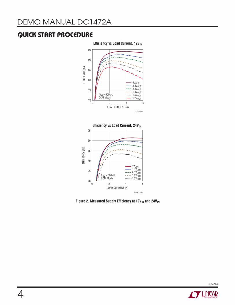
8. For load transient tests, apply an adjustable positive pulse signal between IOSTEP CLK and GND test points. The pulse amplitude sets the load step current amplitude. The pulse width should be short (<1ms) and pulse duty cycle should be low (<15%) to limit the thermal stress on the load transient circuit. The load step current can be monitored with a BNC connected to J6 (10mV/A).

3dc1472af
DEMO MANUAL DC1472A
QUICK START PROCEDURE
Figure 1. Proper Measurement Equipment Setup
+
A
V
–
+
V
+
–
A–+
+ –
VIN
LOAD
4dc1472af
DEMO MANUAL DC1472A
Figure 2. Measured Supply Effi ciency at 12VIN and 24VIN
Effi ciency vs Load Current, 12VIN
Effi ciency vs Load Current, 24VIN
QUICK START PROCEDURE
LOAD CURRENT (A)0
EFFI
CIEN
CY (%
)80
85
DC1472 F02a
75
702 4 6
95
90
5VOUT3.3VOUT2.5VOUT1.8VOUT1.5VOUT1.2VOUT
fSW = 500kHzCCM Mode
LOAD CURRENT (A)0
EFFI
CIEN
CY (%
)
80
85
DC1472 F02b
75
702 4 6
95
90
5VOUT3.3VOUT2.5VOUT1.8VOUT1.5VOUT
fSW = 500kHzCCM Mode
5dc1472af
DEMO MANUAL DC1472A
VIN (V) VOUT (V) COUT BULK COUT CERAMIC
12 1.5 330μF/6.3V POSCAP 1 × 47μF 10V
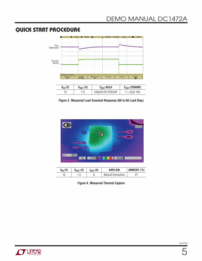
VIN (V) VOUT (V) IOUT (A) AIRFLOW AMBIENT (°C)
12 1.5 6 Natural Convection 27
Figure 3. Measured Load Transient Response (0A to 6A Load Step)
Figure 4. Measured Thermal Capture
QUICK START PROCEDURE
VOUT100mV/DIV
IOUTSTEP5A/DIV
6dc1472af
DEMO MANUAL DC1472A
PARTS LIST
ITEM QTY REFERENCE PART DESCRIPTION MANUFACTURER/PART NUMBER
Required Circuit Components
1 1 C5 CAP, 150μF 35V, ALUM SANYO, 35ME150WXV+TS
2 2 C6, C7 CAP, X5R, 10μF 35V, 1210 TAIYO YUDEN, GMK325BJ106MN-T
3 1 C12 CAP, X5R, 47μF 10V, 1210 TDK, C3225X5R1A476M
4 1 C14 CAP, POSCAP, 330μF 6.3V, 7343 SANYO, 6TPC330MA
5 1 C15 CAP, X5R, 1μF 10V, 0805 AVX, 0805ZD105MAT2A
6 1 C20 CAP, X7R, 0.1μF 16V, 0603 AVX, 0603YC104KAT2A
7 1 R1 RES., 121k 1/16W 1%, 0603 VISHAY, CRCW0603121KFKEA
8 4 R3, R11 RES., 10k 1/16W 1%, 0603 VISHAY, CRCW060310K0FKEA
9 1 R4 RES., 3.16k 1/16W 1%, 0603 VISHAY, CRCW06033K16FKEA
10 1 R5 RES., 60.4k 1/16W 1%, 0603 VISHAY, CRCW060360K4FKEA
11 1 R14 RES., 69.8k 1/16W 1%, 0603 VISHAY, CRCW060369K8FKEA
12 1 R16 RES., 48.7k 1/16W 1%, 0603 VISHAY, CRCW060348K7FKEA
13 1 R17 RES., 28.7k 1/16W 1%, 0603 VISHAY, CRCW060328K7FKEA
14 1 R18 RES., 19.1k 1/16W 1%, 0603 VISHAY, CRCW060319K1FKEA
15 1 R19 RES., 11.5k 1/16W 1%, 0603 VISHAY, CRCW060311K5FKEA
16 1 U1 IC, LTM4618EV LINEAR TECH., LTM4618EV LGA
Additional Demo Board Circuit Components
1 0 C1-C4, C16, C19, C21-C24 CAP, 0603 Optional
2 0 C8, C9, C10, C11, C13 CAP, 1210 Optional
3 2 C17, C18 CAP, X5R, 1μF 10V, 0603 TAIYO YUDEN, LMK107BJ105MA-T
4 0 R6, R8, R10, R12 RES, 0603 Optional
5 4 R7 RES., 10k 1/16W 1%, 0603 VISHAY, CRCW060310K0FKEA
6 1 R9 RES., 0.01Ω 5% 1W, 2512 IRC, LRC-LRF2512LF-01-R010-J
7 1 R15 RES., 10k 1/16W 1%, 0603 VISHAY, CRCW060310K0FKEA
8 1 R2 RES., 100k 1/16W 1%, 0603 VISHAY, CRCW0603100KFKEA
9 1 R13 RES., CHIP, 0, 1/16W, 0603 VISHAY, CRCW06030000Z0EA
10 1 D1 DIODE, ZENER 350MW 4.7V, SOT-23 DIODES INC., BZX84C4V7-7-F
11 1 Q1 XSTR, SUD50N03-10CP MOSFET SILICONIX, SUD50N03-10CP
Hardware
1 10 E1-E10 TP, TURRET, 0.094", PBF MILL-MAX, 2501-2-00-80-00-00-07-0
2 3 JP1, JP2, JP4 JMP, 1X3, 0.079" SAMTEC, TMM-103-02-L-S
3 1 JP3 JMP, 1X4, 0.079" SAMTEC, TMM-104-02-L-S
4 6 JP5, JP6, JP7, JP8, JP9, JP10 JMP, 1X2, 0.079" SAMTEC, TMM-102-02-L-S
5 4 J1, J2, J3, J4 JACK, BANANA KEYSTONE, 575-4
6 2 J5, J6 CONN, BNC, 5 PINS CONNEX, 112404
7 5 JP1-JP4, JP6 SHUNT, 0.079" CENTER SAMTEC, 2SN-BK-G
8 4 4 Corners STANDOFF, SNAP ON, 0.50" KEYSTONE, 8833
7dc1472af
DEMO MANUAL DC1472A
Information furnished by Linear Technology Corporation is believed to be accurate and reliable. However, no responsibility is assumed for its use. Linear Technology Corporation makes no representation that the interconnection of its circuits as described herein will not infringe on existing patent rights.
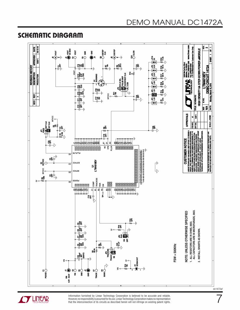
SCHEMATIC DIAGRAM
5 5
4 4
3 3
2 2
1 1
DD
CC
BB
AA
1. A
LL R
ESIS
TORS
ARE
IN O
HMS,
060
3.
ALL
CAP
ACIT
ORS
ARE
IN M
ICRO
FARA
DS, 0
603.
NOTE
: UNL
ESS
OTH
ERW
ISE
SPEC
IFIE
D
2. I
NSTA
LL S
HUNT
S AS
SHO
WN.
FSW
= 5
00KH
z
VOU
T
VIN
5V
INTV
CC
VIN
5V
5V
INTV
CC
INTV
CC
SIZE
DA
TE:
IC N
O.
REV
.
SHEE
TO
F
TITL
E:
APPR
OVA
LS
PCB
DES.
APP
ENG
.
TE
CH
NO
LO
GY
Fax:
(408
)434
-050
7
Milp
itas,
CA
950
35Ph
one:
(408
)432
-190
0
1630
McC
arth
y B
lvd.
LTC
Con
fiden
tial-F
or C
usto
mer
Use
Onl
y
CUST
OM
ER N
OTI
CELI
NEAR
TEC
HNO
LOG
Y HA
S M
ADE
A BE
ST E
FFO
RT T
O D
ESIG
N A
CIRC
UIT
THAT
MEE
TS C
USTO
MER
-SUP
PLIE
D SP
ECIF
ICAT
IONS
;HO
WEV
ER, I
T RE
MAI
NS T
HE C
USTO
MER
'S R
ESPO
NSIB
ILIT
Y TO
VERI
FY P
ROPE
R AN
D RE
LIAB
LE O
PERA
TIO
N IN
THE
ACT
UAL
APPL
ICAT
ION.
CO
MPO
NENT
SUB
STIT
UTIO
N AN
D PR
INTE
DCI
RCUI
T BO
ARD
LAYO
UT M
AY S
IGNI
FICA
NTLY
AFF
ECT
CIRC
UIT
PERF
ORM
ANCE
OR
RELI
ABIL
ITY.
CO
NTAC
T LI
NEAR
TECH
NOLO
GY
APPL
ICAT
IONS
ENG
INEE
RING
FO
R AS
SIST
ANCE
.
THIS
CIR
CUIT
IS P
ROPR
IETA
RY T
O L
INEA
R TE
CHNO
LOG
Y AN
D
SCH
EMA
TIC
SUPP
LIED
FO
R US
E W
ITH
LINE
AR T
ECHN
OLO
GY
PART
S.SC
ALE
= N
ON
E
ww
w.li
near
.com 2
Mon
day,
Mar
ch 15
, 201
01
1
HIG
H DE
NSIT
Y 6A
STE
P-DO
WN
POW
ER u
MO
DULE
KT SAM
Y.
N/A
LTM
4618
EVD
EMO
CIR
CU
IT 1
472A
REVI
SIO
N HI
STO
RYDE
SCRI
PTIO
NDA
TEAP
PRO
VED
ECO
REV
SAM
Y.
PRO
DU
CTI
ON
203
-15-
10
REVI
SIO
N HI
STO
RYDE
SCRI
PTIO
NDA
TEAP
PRO
VED
ECO
REV
SAM
Y.
PRO
DU
CTI
ON
203
-15-
10
REVI
SIO
N HI
STO
RYDE
SCRI
PTIO
NDA
TEAP
PRO
VED
ECO
REV
SAM
Y.
PRO
DU
CTI
ON
203
-15-
10
J6
IOST
EP
J6
IOST
EP
R19
11.5
kR
1911
.5k
C6
10uF
35V
1210
C6
10uF
35V
1210
JP8
2.5V
JP8
2.5V
E2EX
TVC
CE2
EXTV
CC
R18
19.1
kR
1819
.1k
C16
OPTC16
OPT
R3
10k
R3
10k
C13
OPT
1210
C13
OPT
1210
JP7
1.8V
JP7
1.8V
C17
1uF
10V
C17
1uF
10V
TP1
TP1
C19
OPT
C19
OPT
R17
28.7
kR
1728
.7k
R11
10k
R11
10k
C3
OPTC3
OPT
C20
0.1u
FC
200.
1uF
E7TR
AC
KE7
TRA
CK
R9
0.01
2512
R9
0.01
2512
JP5
1.2V
JP5
1.2V
E1PG
OO
DE1
PGO
OD
R16
48.7
kR
1648
.7k
JP4
RU
N
OFFON
JP4
RU
N
OFFON
1 32
J3VO
UT
6A M
AX
J3VO
UT
6A M
AX
C4
OPTC4
OPT
E9SG
ND
E9SG
ND
J1VI
N4.
5V -
26.5
V
J1VI
N4.
5V -
26.5
V
C1
OPT
C1
OPT
C12
47uF
10V
1210
C12
47uF
10V
1210
E3VI
NE3
VIN
U1LT
M46
18EV
U1LT
M46
18EV
GN
DA
4
GNDF6
GNDF7
GNDF5GNDF4GNDF3GNDF2GNDF1
GNDG7GNDG6
NC
A1
INTVCCD3
GNDG5GNDG4
GN
DE4
VIN
A5
SWK
6
VIN
A6
VIN
A7
VOU
TJ1
VOU
TJ2
VIN
B5
VIN
B6
VIN
B7
VIN
C5
VIN
C6
VIN
C7
VOU
TJ3
VOU
TJ4
PLLFLTRA2
TRA
CK
/SS
B1
VOU
TK
1
VOU
TK
2
VOU
TK
3
RU
NB
2
VFB
D1
GN
DE3
PGOODD2
GN
DE2
GN
DE1
VOU
TK
4
VOU
TL1
VOU
TL2
GN
DD
7G
ND
D6
GN
DD
5G
ND
D4
GN
DB
4
GNDG3GNDG2GNDG1
VOU
TL3
VOU
TL4
VOU
TM
1
VOU
TM
2
VOU
TM
3
VOU
TM
4
GN
DE5
GN
DE6
GN
DE7
GNDH1
GNDH2
GNDH3
GNDH4
GNDH5
GNDH6
GNDH7G
ND
J5
GN
DJ6
GN
DJ7
GN
DK
5
GN
DK
7
GN
DL5
GN
DL6
GN
DL7
GN
DM
5
GN
DM
6
GN
DM
7
SGN
DB
3
SGN
DC
2
SGN
DC
3PL
LIN
A3
CO
MP
C1
EXTVCCC4
C15
1uF
10V
0805
C15
1uF
10V
0805
JP6
1.5V
JP6
1.5V
E4VO
UT
E4VO
UT
R14
69.8
kR
1469
.8k
C9
1210
OPT
C9
1210
OPT
+C
1433
0uF
6.3V
7343
+C
1433
0uF
6.3V
7343
R5
60.4
kR
560
.4k
R2
100k
R2
100k
C11
OPT
1210
C11
OPT
1210
R4
3.16
kR
43.
16k
JP2
TRA
CK
/SS
TRA
CK
SS
JP2
TRA
CK
/SS
TRA
CK
SS13 2
C7
10uF
35V
1210
C7
10uF
35V
1210
R6
OPT
R6
OPT
JP1
FREQ
EXT
CLK
INT
CLK
JP1
FREQ
EXT
CLK
INT
CLK
13 2C
23O
PTC
23O
PT
C18
1uF
10V
C18
1uF
10V
E6G
ND
E6G
ND
C10
OPT
1210
C10
OPT
1210
C8
1210
OPT
C8
1210
OPT
C2
OPTC2
OPT
+C
515
0uF
35V
SAN
YO
+C
515
0uF
35V
SAN
YO
R1
121k
R1
121k
D1
BZX
84C
4V7
D1
BZX
84C
4V7
3 1
R7
10k
R7
10k
E10 C
LKIN
E10 C
LKIN
JP3
CC
MB
UR
ST/E
XT C
LKPU
LSE
SKIP
MO
DE/
CLK
SEL
JP3
CC
MB
UR
ST/E
XT C
LKPU
LSE
SKIP
MO
DE/
CLK
SEL
1 32 4
R12
OPT
R12
OPT
R15
10k
R15
10k
R8
OPT
R8
OPT
JP10
5VJP10
5V
Q1
SUD
50N
03Q
1SU
D50
N03
3
1
2
C22
OPT
C22
OPT
R10
OPTR10
OPT
C21
OPT
C21
OPT
E5G
ND
E5G
ND
E8IO
STEP
CLK
E8IO
STEP
CLK
J5
VOU
T
J5
VOU
T
J4
GN
D
J4
GN
D
C24
OPT
C24
OPT
JP9
3.3V
JP9
3.3V
J2
GN
D
J2
GN
D
R13 0R13 0
8dc1472af
DEMO MANUAL DC1472A
Linear Technology Corporation1630 McCarthy Blvd., Milpitas, CA 95035-7417 (408) 432-1900 ● FAX: (408) 434-0507 ● www.linear.com © LINEAR TECHNOLOGY CORPORATION 2010
LT 1010 • PRINTED IN USA
DEMONSTRATION BOARD IMPORTANT NOTICE
Linear Technology Corporation (LTC) provides the enclosed product(s) under the following AS IS conditions:
This demonstration board (DEMO BOARD) kit being sold or provided by Linear Technology is intended for use for ENGINEERING DEVELOPMENT OR EVALUATION PURPOSES ONLY and is not provided by LTC for commercial use. As such, the DEMO BOARD herein may not be complete in terms of required design-, marketing-, and/or manufacturing-related protective considerations, including but not limited to product safety measures typically found in finished commercial goods. As a prototype, this product does not fall within the scope of the European Union direc-tive on electromagnetic compatibility and therefore may or may not meet the technical requirements of the directive, or other regulations.
If this evaluation kit does not meet the specifications recited in the DEMO BOARD manual the kit may be returned within 30 days from the date of delivery for a full refund. THE FOREGOING WARRANTY IS THE EXCLUSIVE WARRANTY MADE BY THE SELLER TO BUYER AND IS IN LIEU OF ALL OTHER WARRANTIES, EXPRESSED, IMPLIED, OR STATUTORY, INCLUDING ANY WARRANTY OF MERCHANTABILITY OR FITNESS FOR ANY PARTICULAR PURPOSE. EXCEPT TO THE EXTENT OF THIS INDEMNITY, NEITHER PARTY SHALL BE LIABLE TO THE OTHER FOR ANY INDIRECT, SPECIAL, INCIDENTAL, OR CONSEQUENTIAL DAMAGES.
The user assumes all responsibility and liability for proper and safe handling of the goods. Further, the user releases LTC from all claims arising from the handling or use of the goods. Due to the open construction of the product, it is the user’s responsibility to take any and all appropriate precautions with regard to electrostatic discharge. Also be aware that the products herein may not be regulatory compliant or agency certified (FCC, UL, CE, etc.).
No License is granted under any patent right or other intellectual property whatsoever. LTC assumes no liability for applications assistance, customer product design, software performance, or infringement of patents or any other intellectual property rights of any kind.
LTC currently services a variety of customers for products around the world, and therefore this transaction is not exclusive.
Please read the DEMO BOARD manual prior to handling the product. Persons handling this product must have electronics training and observe good laboratory practice standards. Common sense is encouraged.
This notice contains important safety information about temperatures and voltages. For further safety concerns, please contact a LTC applica-tion engineer.
Mailing Address:
Linear Technology
1630 McCarthy Blvd.
Milpitas, CA 95035
Copyright © 2004, Linear Technology Corporation