![Some improvements of Xfem for cracked domainsmath.univ-lyon1.fr/~renard/papers/2007_CMAS.pdf · Some improvements of Xfem for cracked domains 3. θ ∈ ]−π,π[r crack tip ΓC.](https://static.fdocument.org/doc/165x107/5aa80e8f7f8b9aca258b5764/some-improvements-of-xfem-for-cracked-renardpapers2007cmaspdfsome-improvements.jpg)
Datasheet - STD4N62K3 - st.com · This MDmesh™ K3 Power MOSFET is the result of improvements...
20
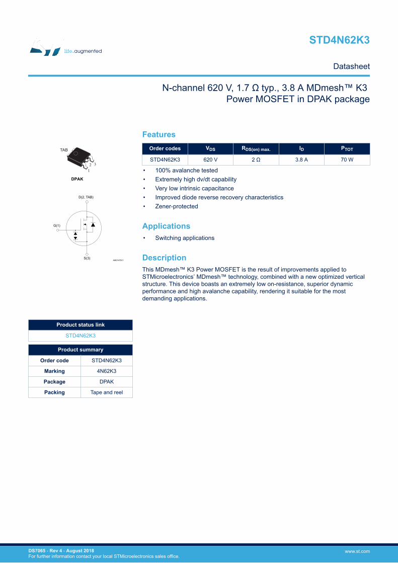
1 3 TAB 2 DPAK D(2, TAB) G(1) S(3) AM01475V1 Features Order codes V DS R DS(on) max. I D P TOT STD4N62K3 620 V 2 Ω 3.8 A 70 W • 100% avalanche tested • Extremely high dv/dt capability • Very low intrinsic capacitance • Improved diode reverse recovery characteristics • Zener-protected Applications • Switching applications Description This MDmesh™ K3 Power MOSFET is the result of improvements applied to STMicroelectronics’ MDmesh™ technology, combined with a new optimized vertical structure. This device boasts an extremely low on-resistance, superior dynamic performance and high avalanche capability, rendering it suitable for the most demanding applications. Product status link STD4N62K3 Product summary Order code STD4N62K3 Marking 4N62K3 Package DPAK Packing Tape and reel N-channel 620 V, 1.7 Ω typ., 3.8 A MDmesh™ K3 Power MOSFET in DPAK package STD4N62K3 Datasheet DS7065 - Rev 4 - August 2018 For further information contact your local STMicroelectronics sales office. www.st.com
Transcript of Datasheet - STD4N62K3 - st.com · This MDmesh™ K3 Power MOSFET is the result of improvements...
13
TAB
2
DPAK
D(2, TAB)
G(1)
S(3)AM01475V1
FeaturesOrder codes VDS RDS(on) max. ID PTOT
STD4N62K3 620 V 2 Ω 3.8 A 70 W
• 100% avalanche tested• Extremely high dv/dt capability• Very low intrinsic capacitance• Improved diode reverse recovery characteristics• Zener-protected
Applications• Switching applications
DescriptionThis MDmesh™ K3 Power MOSFET is the result of improvements applied toSTMicroelectronics’ MDmesh™ technology, combined with a new optimized verticalstructure. This device boasts an extremely low on-resistance, superior dynamicperformance and high avalanche capability, rendering it suitable for the mostdemanding applications.
Product status link
STD4N62K3
Product summary
Order code STD4N62K3
Marking 4N62K3
Package DPAK
Packing Tape and reel
N-channel 620 V, 1.7 Ω typ., 3.8 A MDmesh™ K3 Power MOSFET in DPAK package
STD4N62K3
Datasheet
DS7065 - Rev 4 - August 2018For further information contact your local STMicroelectronics sales office.
www.st.com
1 Electrical ratings
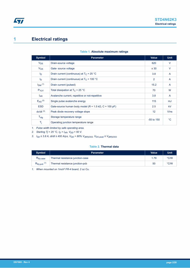
Table 1. Absolute maximum ratings
Symbol Parameter Value Unit
VDS Drain-source voltage 620 V
VGS Gate- source voltage ± 30 V
ID Drain current (continuous) at TC = 25 °C 3.8 A
ID Drain current (continuous) at TC = 100 °C 2 A
IDM (1) Drain current (pulsed) 15.2 A
PTOT Total dissipation at TC = 25 °C 70 W
IAR Avalanche current, repetitive or not-repetitive 3.8 A
EAS (2) Single pulse avalanche energy 115 mJ
ESD Gate-source human body model (R = 1.5 kΩ, C = 100 pF) 2.5 kV
dv/dt (3) Peak diode recovery voltage slope 12 V/ns
Tstg Storage temperature range-55 to 150 °C
Tj Operating junction temperature range
1. Pulse width limited by safe operating area.2. Starting Tj = 25 °C, ID = IAR, VDD = 50 V.
3. ISD ≤ 3.8 A, di/dt ≤ 400 A/µs, VDD = 80% V(BR)DSS, VDS peak ≤ V(BR)DSS.
Table 2. Thermal data
Symbol Parameter Value Unit
Rthj-case Thermal resistance junction-case 1.79 °C/W
Rthj-pcb (1) Thermal resistance junction-pcb 50 °C/W
1. When mounted on 1inch² FR-4 board, 2 oz Cu.
STD4N62K3Electrical ratings
DS7065 - Rev 4 page 2/20
2 Electrical characteristics
(TC = 25 °C unless otherwise specified)
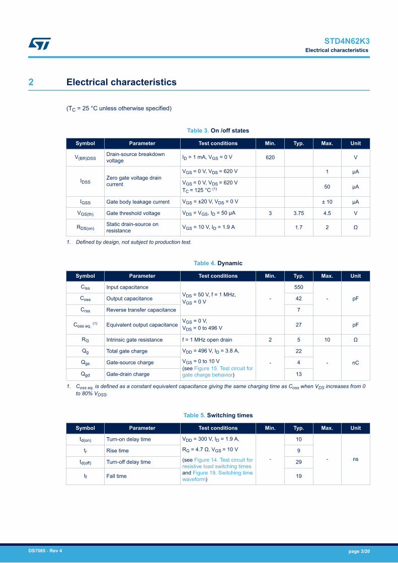
Table 3. On /off states
Symbol Parameter Test conditions Min. Typ. Max. Unit
V(BR)DSSDrain-source breakdownvoltage ID = 1 mA, VGS = 0 V 620 V
IDSSZero gate voltage draincurrent
VGS = 0 V, VDS = 620 V 1 µA
VGS = 0 V, VDS = 620 VTC = 125 °C (1) 50 µA
IGSS Gate body leakage current VGS = ±20 V, VDS = 0 V ± 10 µA
VGS(th) Gate threshold voltage VDS = VGS, ID = 50 µA 3 3.75 4.5 V
RDS(on)Static drain-source onresistance VGS = 10 V, ID = 1.9 A 1.7 2 Ω
1. Defined by design, not subject to production test.
Table 4. Dynamic
Symbol Parameter Test conditions Min. Typ. Max. Unit
Ciss Input capacitanceVDS = 50 V, f = 1 MHz,VGS = 0 V -
550
- pFCoss Output capacitance 42
Crss Reverse transfer capacitance 7
Coss eq. (1) Equivalent output capacitanceVGS = 0 V,VDS = 0 to 496 V 27 pF
RG Intrinsic gate resistance f = 1 MHz open drain 2 5 10 Ω
Qg Total gate charge VDD = 496 V, ID = 3.8 A,
VGS = 0 to 10 V(see Figure 15. Test circuit forgate charge behavior)
-
22
- nCQgs Gate-source charge 4
Qgd Gate-drain charge 13
1. Coss eq. is defined as a constant equivalent capacitance giving the same charging time as Coss when VDS increases from 0to 80% VDSS.
Table 5. Switching times
Symbol Parameter Test conditions Min. Typ. Max. Unit
td(on) Turn-on delay time VDD = 300 V, ID = 1.9 A,
RG = 4.7 Ω, VGS = 10 V
(see Figure 14. Test circuit forresistive load switching timesand Figure 19. Switching timewaveform)
-
10
- nstr Rise time 9
td(off) Turn-off delay time 29
tf Fall time 19
STD4N62K3Electrical characteristics
DS7065 - Rev 4 page 3/20
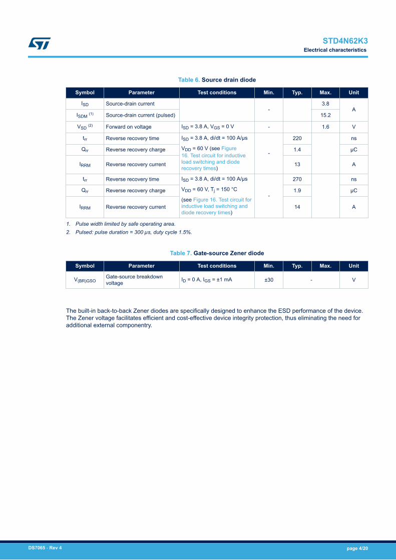
Table 6. Source drain diode
Symbol Parameter Test conditions Min. Typ. Max. Unit
ISD Source-drain current-
3.8A
ISDM (1) Source-drain current (pulsed) 15.2
VSD (2) Forward on voltage ISD = 3.8 A, VGS = 0 V - 1.6 V
trr Reverse recovery time ISD = 3.8 A, di/dt = 100 A/µs
VDD = 60 V (see Figure16. Test circuit for inductiveload switching and dioderecovery times)
-
220 ns
Qrr Reverse recovery charge 1.4 μC
IRRM Reverse recovery current 13 A
trr Reverse recovery time ISD = 3.8 A, di/dt = 100 A/µs
VDD = 60 V, Tj = 150 °C
(see Figure 16. Test circuit forinductive load switching anddiode recovery times)
-
270 ns
Qrr Reverse recovery charge 1.9 μC
IRRM Reverse recovery current 14 A
1. Pulse width limited by safe operating area.2. Pulsed: pulse duration = 300 µs, duty cycle 1.5%.
Table 7. Gate-source Zener diode
Symbol Parameter Test conditions Min. Typ. Max. Unit
V(BR)GSOGate-source breakdownvoltage ID = 0 A, IGS = ±1 mA ±30 - V
The built-in back-to-back Zener diodes are specifically designed to enhance the ESD performance of the device.The Zener voltage facilitates efficient and cost-effective device integrity protection, thus eliminating the need foradditional external componentry.
STD4N62K3Electrical characteristics
DS7065 - Rev 4 page 4/20
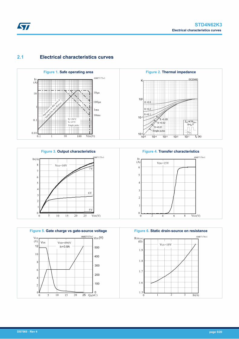
2.1 Electrical characteristics curves
Figure 1. Safe operating area
ID
10
1
0.1
0.01 0.1 1 100 VDS(V) 10
(A)
Opera tion in
this
a rea is
Limite
d by max R
DS(on)
10µs
100µs
1ms
10msTj=150°C Tc=25°C Single pulse
AM07173v1
Figure 2. Thermal impedance
GC20460
100
10-1
10-2
10-5 10-4 10-3 10-2 10-1
K
tp (s)
Figure 3. Output characteristics
ID
3
2
1
0 0 10 VDS(V) 20
(A)
5 15 25
4
5
5V
6V
7VVGS=10V
6
7
8
AM07175v1
Figure 4. Transfer characteristics
ID
3
2
1
00 4 VGS(V)8
(A)
2 6
4
5
6VDS=15V
AM07176v1
Figure 5. Gate charge vs gate-source voltage
VGS
6
4
2
0 0 5 Qg(nC)
(V)
20
8
10 15
10
VDD=496V ID
DS
DS (V)
Figure 6. Static drain-source on resistance
RDS(on)
1.8
1.7
1.6
1.5 0 2 ID(A)
(Ω)
1 3
1.9
VGS=10V
AM07178v1
STD4N62K3Electrical characteristics curves
DS7065 - Rev 4 page 5/20
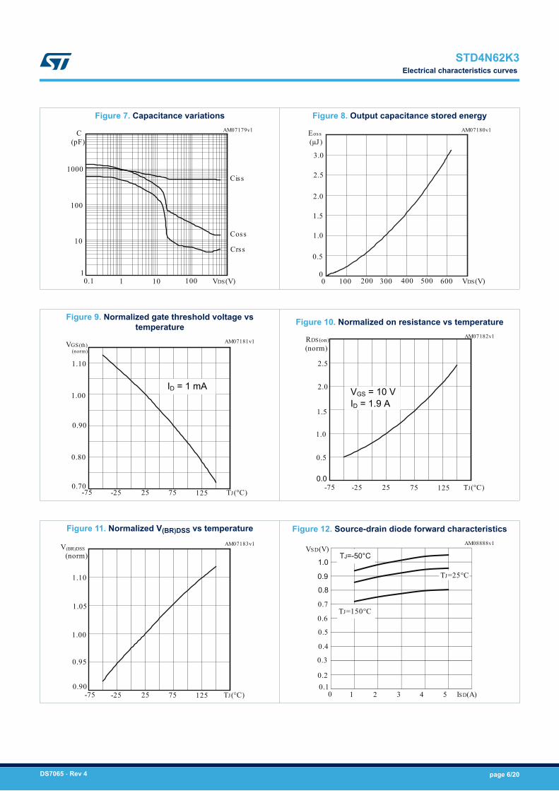
Figure 7. Capacitance variations
C
1000
100
10
1 0.1 10 VDS(V)
(pF)
1 100
Ciss
Coss
Crss
AM07179v1
Figure 8. Output capacitance stored energy
Eoss
1.5
1.0
0.5
0 0 100 VDS(V)
(µJ)
400
2.0
200 300
2.5
3.0
500 600
AM07180v1
Figure 9. Normalized gate threshold voltage vstemperature
VGS(th)
1.00
0.90
0.80
0.70 -75 TJ(°C)
(norm)
-25
1.10
75 25 125
AM07181v1
ID = 1 mA
Figure 10. Normalized on resistance vs temperature
RDS(on)
2.0
1.5
1.0
0.5
-75 TJ(°C)
(norm)
-25 25 75 125
2.5
AM07182v1
0.0
VGS = 10 VID = 1.9 A
Figure 11. Normalized V(BR)DSS vs temperature
V(BR)DSS
-75 TJ(°C)
(norm)
-25 75 25 125 0.90
0.95
1.00
1.05
1.10
AM07183v1
Figure 12. Source-drain diode forward characteristics
VSD
0 2 ISD(A)
(V)
1 5 3 4 0.1 0.2
0.3
0.4
0.5
0.6
0.7
TJ=25°C
TJ=150°C
AM08888v1
STD4N62K3Electrical characteristics curves
DS7065 - Rev 4 page 6/20
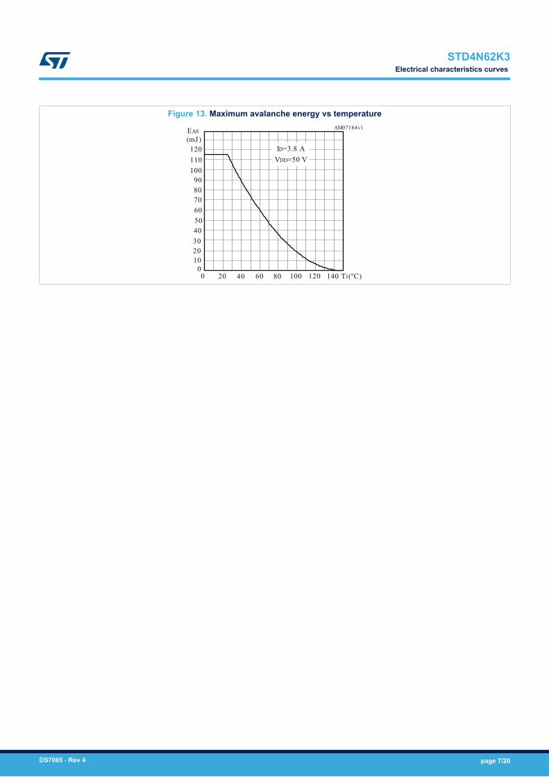
Figure 13. Maximum avalanche energy vs temperature
EAS
0 40 TJ(°C)
(mJ)
20 100 60 80 0
10 20 30 40
120 140
50 60 70 80
100 110 120 ID=3.8 A
VDD=50 V
90
AM07184v1
STD4N62K3Electrical characteristics curves
DS7065 - Rev 4 page 7/20
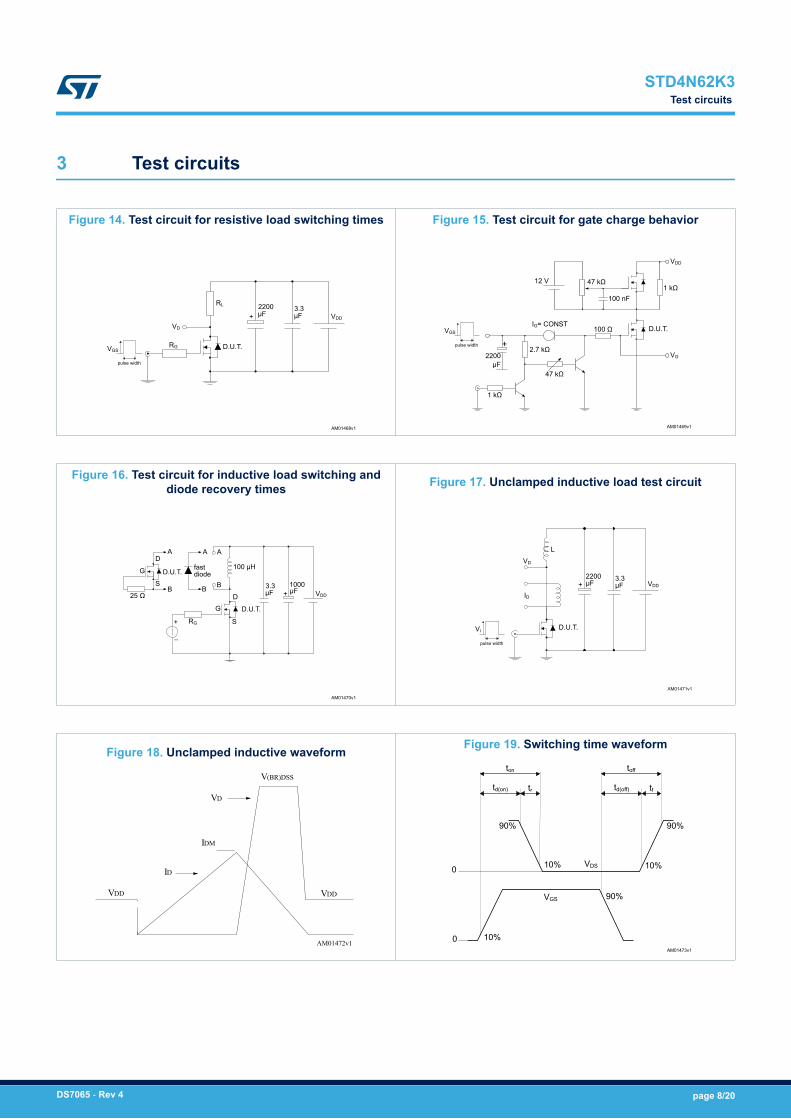
3 Test circuits
Figure 14. Test circuit for resistive load switching times
AM01468v1
VD
RG
RL
D.U.T.
2200μF VDD
3.3μF+
pulse width
VGS
Figure 15. Test circuit for gate charge behavior
AM01469v1
47 kΩ1 kΩ
47 kΩ
2.7 kΩ
1 kΩ
12 V
IG= CONST100 Ω
100 nF
D.U.T.
+pulse width
VGS
2200μF
VG
VDD
Figure 16. Test circuit for inductive load switching anddiode recovery times
AM01470v1
AD
D.U.T.S
B
G
25 Ω
A A
B B
RG
GD
S
100 µH
µF3.3 1000
µF VDD
D.U.T.
+
_
+
fastdiode
Figure 17. Unclamped inductive load test circuit
AM01471v1
VD
ID
D.U.T.
L
VDD+
pulse width
Vi
3.3µF
2200µF
Figure 18. Unclamped inductive waveform
AM01472v1
V(BR)DSS
VDDVDD
VD
IDM
ID
Figure 19. Switching time waveform
AM01473v1
0
VGS 90%
VDS
90%
10%
90%
10%
10%
ton
td(on) tr
0
toff
td(off) tf
STD4N62K3Test circuits
DS7065 - Rev 4 page 8/20
4 Package information
In order to meet environmental requirements, ST offers these devices in different grades of ECOPACK®
packages, depending on their level of environmental compliance. ECOPACK® specifications, grade definitionsand product status are available at: www.st.com. ECOPACK® is an ST trademark.
STD4N62K3Package information
DS7065 - Rev 4 page 9/20
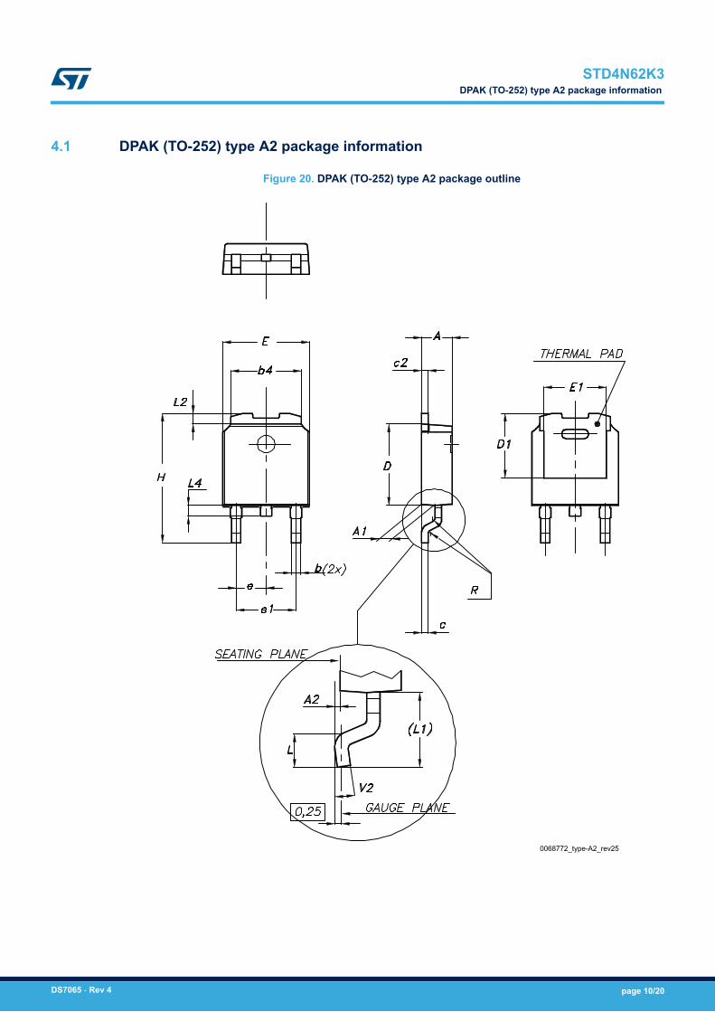
4.1 DPAK (TO-252) type A2 package information
Figure 20. DPAK (TO-252) type A2 package outline
0068772_type-A2_rev25
STD4N62K3DPAK (TO-252) type A2 package information
DS7065 - Rev 4 page 10/20
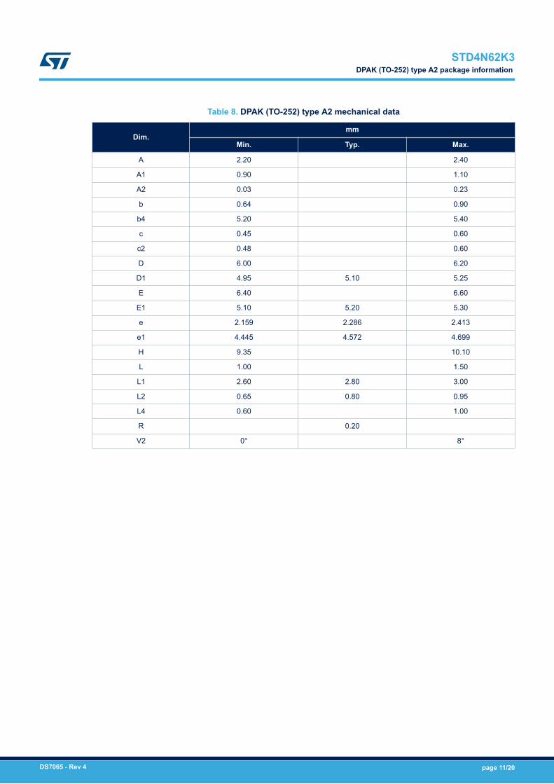
Table 8. DPAK (TO-252) type A2 mechanical data
Dim.mm
Min. Typ. Max.
A 2.20 2.40
A1 0.90 1.10
A2 0.03 0.23
b 0.64 0.90
b4 5.20 5.40
c 0.45 0.60
c2 0.48 0.60
D 6.00 6.20
D1 4.95 5.10 5.25
E 6.40 6.60
E1 5.10 5.20 5.30
e 2.159 2.286 2.413
e1 4.445 4.572 4.699
H 9.35 10.10
L 1.00 1.50
L1 2.60 2.80 3.00
L2 0.65 0.80 0.95
L4 0.60 1.00
R 0.20
V2 0° 8°
STD4N62K3DPAK (TO-252) type A2 package information
DS7065 - Rev 4 page 11/20
4.2 DPAK (TO-252) type C2 package information
Figure 21. DPAK (TO-252) type C2 package outline
0068772_C2_25
STD4N62K3DPAK (TO-252) type C2 package information
DS7065 - Rev 4 page 12/20
Table 9. DPAK (TO-252) type C2 mechanical data
Dim.mm
Min. Typ. Max.
A 2.20 2.30 2.38
A1 0.90 1.01 1.10
A2 0.00 0.10
b 0.72 0.85
b4 5.13 5.33 5.46
c 0.47 0.60
c2 0.47 0.60
D 6.00 6.10 6.20
D1 5.10 5.60
E 6.50 6.60 6.70
E1 5.20 5.50
e 2.186 2.286 2.386
H 9.80 10.10 10.40
L 1.40 1.50 1.70
L1 2.90 REF
L2 0.90 1.25
L3 0.51 BSC
L4 0.60 0.80 1.00
L6 1.80 BSC
θ1 5° 7° 9°
θ2 5° 7° 9°
V2 0° 8°
STD4N62K3DPAK (TO-252) type C2 package information
DS7065 - Rev 4 page 13/20
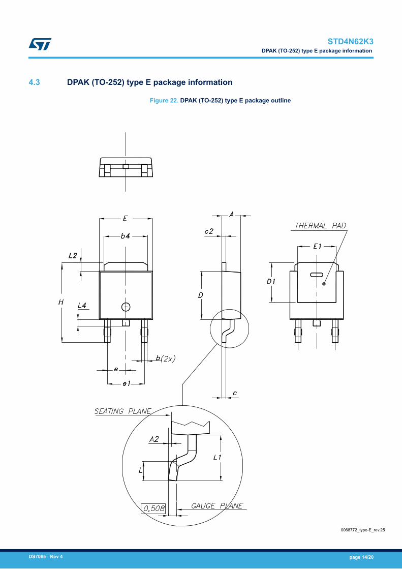
4.3 DPAK (TO-252) type E package information
Figure 22. DPAK (TO-252) type E package outline
0068772_type-E_rev.25
STD4N62K3DPAK (TO-252) type E package information
DS7065 - Rev 4 page 14/20
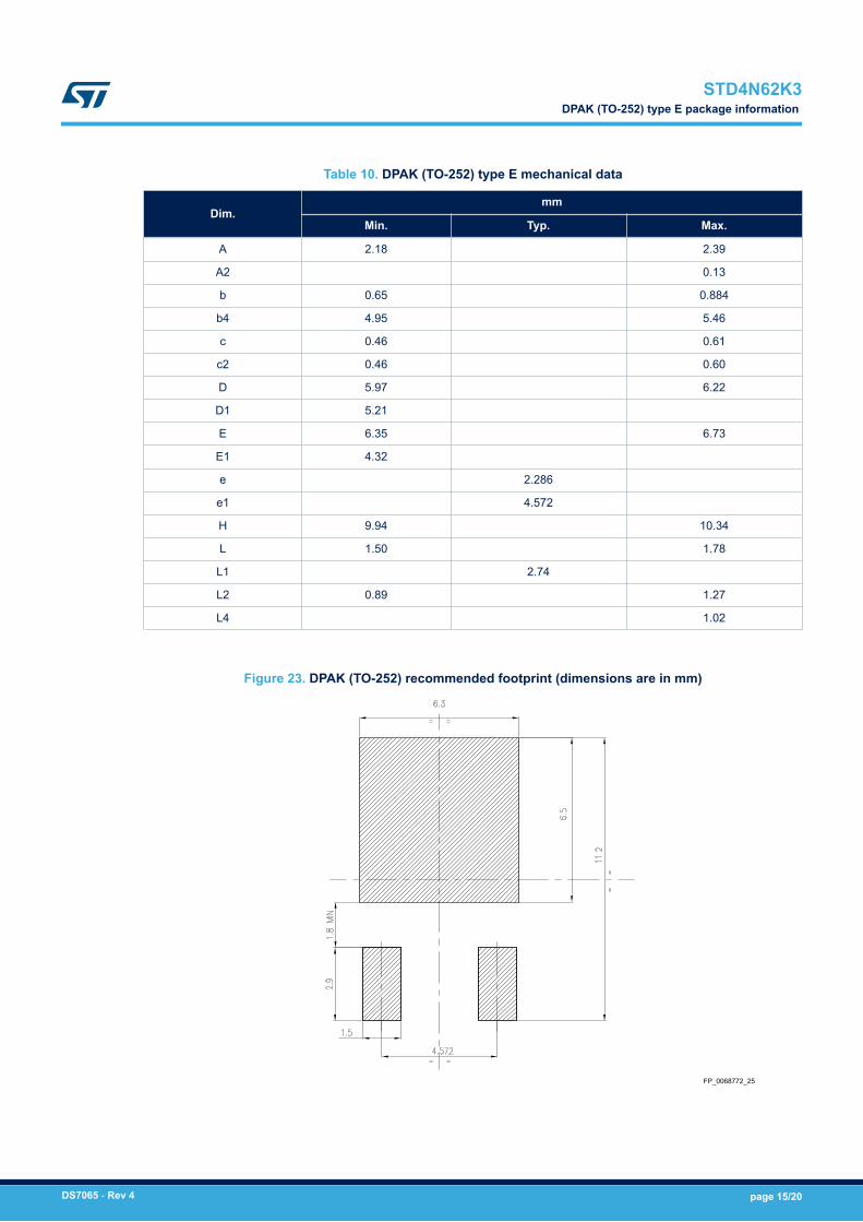
Table 10. DPAK (TO-252) type E mechanical data
Dim.mm
Min. Typ. Max.
A 2.18 2.39
A2 0.13
b 0.65 0.884
b4 4.95 5.46
c 0.46 0.61
c2 0.46 0.60
D 5.97 6.22
D1 5.21
E 6.35 6.73
E1 4.32
e 2.286
e1 4.572
H 9.94 10.34
L 1.50 1.78
L1 2.74
L2 0.89 1.27
L4 1.02
Figure 23. DPAK (TO-252) recommended footprint (dimensions are in mm)
FP_0068772_25
STD4N62K3DPAK (TO-252) type E package information
DS7065 - Rev 4 page 15/20
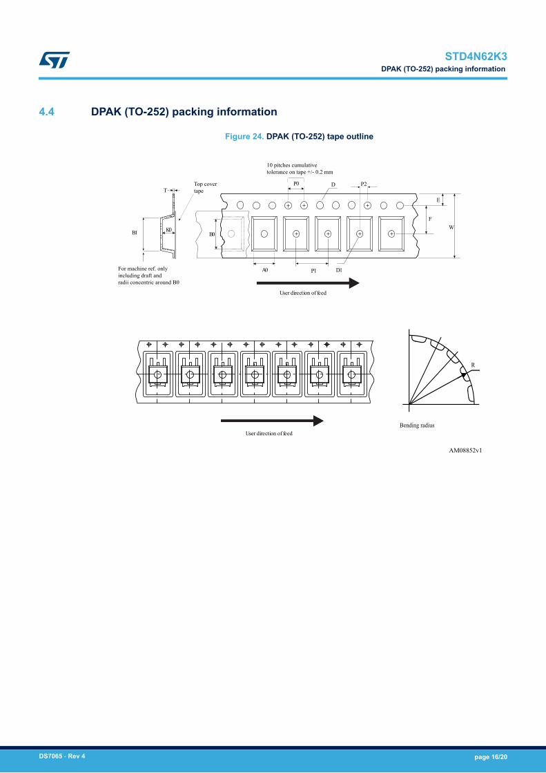
4.4 DPAK (TO-252) packing information
Figure 24. DPAK (TO-252) tape outline
P1A0 D1
P0
FW
E
D
B0K0
T
User direction of feed
P2
10 pitches cumulativetolerance on tape +/- 0.2 mm
User direction of feed
R
Bending radius
B1
For machine ref. onlyincluding draft andradii concentric around B0
AM08852v1
Top covertape
STD4N62K3DPAK (TO-252) packing information
DS7065 - Rev 4 page 16/20
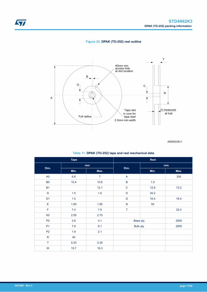
Figure 25. DPAK (TO-252) reel outline
A
D
B
Full radius
Tape slot in core for tape start
2.5mm min.width
G measured at hub
C
N
40mm min. access hole at slot location
T
AM06038v1
Table 11. DPAK (TO-252) tape and reel mechanical data
Tape Reel
Dim.mm
Dim.mm
Min. Max. Min. Max.
A0 6.8 7 A 330
B0 10.4 10.6 B 1.5
B1 12.1 C 12.8 13.2
D 1.5 1.6 D 20.2
D1 1.5 G 16.4 18.4
E 1.65 1.85 N 50
F 7.4 7.6 T 22.4
K0 2.55 2.75
P0 3.9 4.1 Base qty. 2500
P1 7.9 8.1 Bulk qty. 2500
P2 1.9 2.1
R 40
T 0.25 0.35
W 15.7 16.3
STD4N62K3DPAK (TO-252) packing information
DS7065 - Rev 4 page 17/20

Revision history
Table 12. Document revision history
Date Revision Changes
16-Dec-2010 1 First release.
26-Apr-2012 2
Added min and max values for RG in Table 5: Dynamic and
Section 5: Packaging mechanical data.
Updated Section 4: Package mechanical data.
Minor text changes.
09-Sep-2013 3– Updated: Section 4: Package mechanical data
– Minor text changes
03-Aug-2018 4
The part number STB4N62K3 has been moved to a separate datasheet.
Removed maturity status indication from cover page. The document status is production data.
Updated title and features in cover page.
Updated Section 1 Electrical ratings, Section 2 Electrical characteristics and Section4 Package information.
Minor text changes.
STD4N62K3
DS7065 - Rev 4 page 18/20
Contents
1 Electrical ratings . . . . . . . . . . . . . . . . . . . . . . . . . . . . . . . . . . . . . . . . . . . . . . . . . . . . . . . . . . . . . . . . . .2
2 Electrical characteristics. . . . . . . . . . . . . . . . . . . . . . . . . . . . . . . . . . . . . . . . . . . . . . . . . . . . . . . . . . .3
2.1 Electrical characteristics curves . . . . . . . . . . . . . . . . . . . . . . . . . . . . . . . . . . . . . . . . . . . . . . . . . . 5
3 Test circuits . . . . . . . . . . . . . . . . . . . . . . . . . . . . . . . . . . . . . . . . . . . . . . . . . . . . . . . . . . . . . . . . . . . . . . .8
4 Package information. . . . . . . . . . . . . . . . . . . . . . . . . . . . . . . . . . . . . . . . . . . . . . . . . . . . . . . . . . . . . . .9
4.1 DPAK (TO-252) type A2 package information . . . . . . . . . . . . . . . . . . . . . . . . . . . . . . . . . . . . . . . 9
4.2 DPAK (TO-252) type C2 package information . . . . . . . . . . . . . . . . . . . . . . . . . . . . . . . . . . . . . . 11
4.3 DPAK (TO-252) type E package information . . . . . . . . . . . . . . . . . . . . . . . . . . . . . . . . . . . . . . . 13
4.4 DPAK (TO-252) packing information. . . . . . . . . . . . . . . . . . . . . . . . . . . . . . . . . . . . . . . . . . . . . . 15
Revision history . . . . . . . . . . . . . . . . . . . . . . . . . . . . . . . . . . . . . . . . . . . . . . . . . . . . . . . . . . . . . . . . . . . . . . .18
STD4N62K3Contents
DS7065 - Rev 4 page 19/20
IMPORTANT NOTICE – PLEASE READ CAREFULLY
STMicroelectronics NV and its subsidiaries (“ST”) reserve the right to make changes, corrections, enhancements, modifications, and improvements to STproducts and/or to this document at any time without notice. Purchasers should obtain the latest relevant information on ST products before placing orders. STproducts are sold pursuant to ST’s terms and conditions of sale in place at the time of order acknowledgement.
Purchasers are solely responsible for the choice, selection, and use of ST products and ST assumes no liability for application assistance or the design ofPurchasers’ products.
No license, express or implied, to any intellectual property right is granted by ST herein.
Resale of ST products with provisions different from the information set forth herein shall void any warranty granted by ST for such product.
ST and the ST logo are trademarks of ST. All other product or service names are the property of their respective owners.
Information in this document supersedes and replaces information previously supplied in any prior versions of this document.
© 2018 STMicroelectronics – All rights reserved
STD4N62K3
DS7065 - Rev 4 page 20/20