Datasheet - STD13N60DM2 - N-channel 600 V, 0.310 Ω typ ... · for inductive load switching and...
16
1 3 TAB 2 DPAK D(2, TAB) G(1) S(3) AM01475V1 Order codes V DS R DS(on) max. I D STD13N60DM2 600 V 0.365 Ω 11 A • Fast-recovery body diode • Extremely low gate charge and input capacitance • Low on-resistance • 100% avalanche tested • Extremely high dv/dt ruggedness • Zener-protected Applications • Switching applications Description This high-voltage N-channel Power MOSFET is part of the MDmesh™ DM2 fast- recovery diode series. It offers very low recovery charge (Q rr ) and time (t rr ) combined with low R DS(on) , rendering it suitable for the most demanding high-efficiency converters and ideal for bridge topologies and ZVS phase-shift converters. Product status links STD13N60DM2 Product summary Order code STD13N60DM2 Marking 13N60DM2 Package DPAK Packing Tape and reel N-channel 600 V, 0.310 Ω typ., 11 A MDmesh™ DM2 Power MOSFET in a DPAK package STD13N60DM2 Datasheet DS11596 - Rev 3 - November 2018 For further information contact your local STMicroelectronics sales office. www.st.com
Transcript of Datasheet - STD13N60DM2 - N-channel 600 V, 0.310 Ω typ ... · for inductive load switching and...
13
TAB
2
DPAK
D(2, TAB)
G(1)
S(3)AM01475V1
Order codes VDS RDS(on) max. ID
STD13N60DM2 600 V 0.365 Ω 11 A
• Fast-recovery body diode• Extremely low gate charge and input capacitance• Low on-resistance• 100% avalanche tested• Extremely high dv/dt ruggedness• Zener-protected
Applications• Switching applications
DescriptionThis high-voltage N-channel Power MOSFET is part of the MDmesh™ DM2 fast-recovery diode series. It offers very low recovery charge (Qrr) and time (trr) combinedwith low RDS(on), rendering it suitable for the most demanding high-efficiencyconverters and ideal for bridge topologies and ZVS phase-shift converters.
Product status links
STD13N60DM2
Product summary
Order code STD13N60DM2
Marking 13N60DM2
Package DPAK
Packing Tape and reel
N-channel 600 V, 0.310 Ω typ., 11 A MDmesh™ DM2 Power MOSFET in a DPAK package
STD13N60DM2
Datasheet
DS11596 - Rev 3 - November 2018For further information contact your local STMicroelectronics sales office.
www.st.com
1 Electrical ratings
Table 1. Absolute maximum ratings
Symbol Parameter Value Unit
VGS Gate-source voltage ±25 V
IDDrain current (continuous) at Tcase = 25 °C 11
ADrain current (continuous) at Tcase = 100 °C 7
IDM (1) Drain current (pulsed) 44 A
PTOT Total power dissipation at Tcase = 25 °C 110 W
dv/dt (2) Peak diode recovery voltage slope 40V/ns
dv/dt(3) MOSFET dv/dt ruggedness 50
Tstg Storage temperature range-55 to 150 °C
Tj Operating junction temperature range
1. Pulse width limited by safe operating area.2. ISD ≤ 11 A, di/dt ≤ 900 A/μs; VDS peak < V(BR)DSS, VDD=400 V.
3. VDS ≤ 480 V.
Table 2. Thermal data
Symbol Parameter Value Unit
Rthj-case Thermal resistance junction-case 1.14°C/W
Rthj-pcb (1) Thermal resistance junction-pcb 50
1. When mounted on FR-4 board of inch², 2oz Cu.
Table 3. Avalanche characteristics
Symbol Parameter Value Unit
IARAvalanche current, repetitive or not repetitive(Pulse width limited by Tjmax)
2.5 A
EASSingle pulse avalanche energy
(starting Tj = 25 °C, ID = IAR, VDD = 50 V)340 mJ
STD13N60DM2Electrical ratings
DS11596 - Rev 3 page 2/16
2 Electrical characteristics
(Tcase = 25 °C unless otherwise specified)
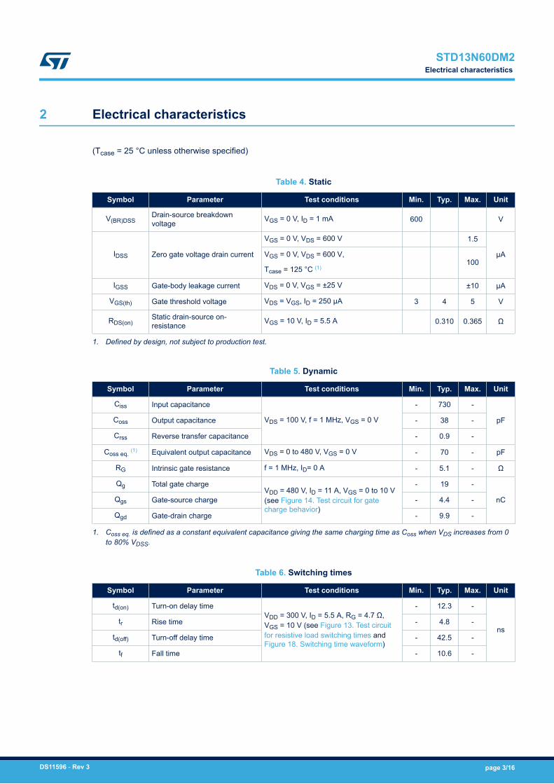
Table 4. Static
Symbol Parameter Test conditions Min. Typ. Max. Unit
V(BR)DSSDrain-source breakdownvoltage VGS = 0 V, ID = 1 mA 600 V
IDSS Zero gate voltage drain current
VGS = 0 V, VDS = 600 V 1.5
µAVGS = 0 V, VDS = 600 V,
Tcase = 125 °C (1)100
IGSS Gate-body leakage current VDS = 0 V, VGS = ±25 V ±10 µA
VGS(th) Gate threshold voltage VDS = VGS, ID = 250 µA 3 4 5 V
RDS(on)Static drain-source on-resistance VGS = 10 V, ID = 5.5 A 0.310 0.365 Ω
1. Defined by design, not subject to production test.
Table 5. Dynamic
Symbol Parameter Test conditions Min. Typ. Max. Unit
Ciss Input capacitance
VDS = 100 V, f = 1 MHz, VGS = 0 V
- 730 -
pFCoss Output capacitance - 38 -
Crss Reverse transfer capacitance - 0.9 -
Coss eq. (1) Equivalent output capacitance VDS = 0 to 480 V, VGS = 0 V - 70 - pF
RG Intrinsic gate resistance f = 1 MHz, ID= 0 A - 5.1 - Ω
Qg Total gate chargeVDD = 480 V, ID = 11 A, VGS = 0 to 10 V(see Figure 14. Test circuit for gatecharge behavior)
- 19 -
nCQgs Gate-source charge - 4.4 -
Qgd Gate-drain charge - 9.9 -
1. Coss eq. is defined as a constant equivalent capacitance giving the same charging time as Coss when VDS increases from 0to 80% VDSS.
Table 6. Switching times
Symbol Parameter Test conditions Min. Typ. Max. Unit
td(on) Turn-on delay timeVDD = 300 V, ID = 5.5 A, RG = 4.7 Ω,VGS = 10 V (see Figure 13. Test circuitfor resistive load switching times andFigure 18. Switching time waveform)
- 12.3 -
nstr Rise time - 4.8 -
td(off) Turn-off delay time - 42.5 -
tf Fall time - 10.6 -
STD13N60DM2Electrical characteristics
DS11596 - Rev 3 page 3/16
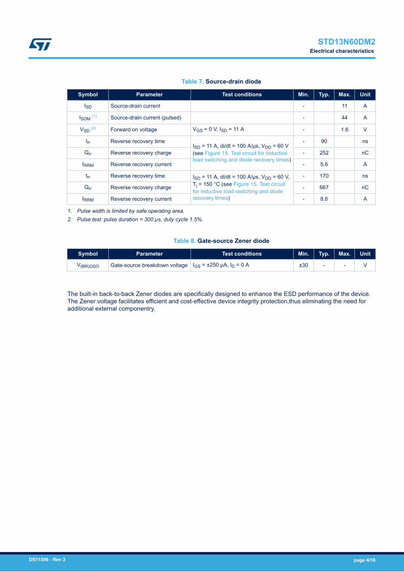
Table 7. Source-drain diode
Symbol Parameter Test conditions Min. Typ. Max. Unit
ISD Source-drain current - 11 A
ISDM (1) Source-drain current (pulsed) - 44 A
VSD (2) Forward on voltage VGS = 0 V, ISD = 11 A - 1.6 V
trr Reverse recovery timeISD = 11 A, di/dt = 100 A/µs, VDD = 60 V(see Figure 15. Test circuit for inductiveload switching and diode recovery times)
- 90 ns
Qrr Reverse recovery charge - 252 nC
IRRM Reverse recovery current - 5.6 A
trr Reverse recovery time ISD = 11 A, di/dt = 100 A/µs, VDD = 60 V,Tj = 150 °C (see Figure 15. Test circuitfor inductive load switching and dioderecovery times)
- 170 ns
Qrr Reverse recovery charge - 667 nC
IRRM Reverse recovery current - 8.6 A
1. Pulse width is limited by safe operating area.2. Pulse test: pulse duration = 300 µs, duty cycle 1.5%.
Table 8. Gate-source Zener diode
Symbol Parameter Test conditions Min. Typ. Max. Unit
V(BR)GSO Gate-source breakdown voltage IGS = ±250 μA, ID = 0 A ±30 - - V
The built-in back-to-back Zener diodes are specifically designed to enhance the ESD performance of the device.The Zener voltage facilitates efficient and cost-effective device integrity protection,thus eliminating the need foradditional external componentry.
STD13N60DM2Electrical characteristics
DS11596 - Rev 3 page 4/16
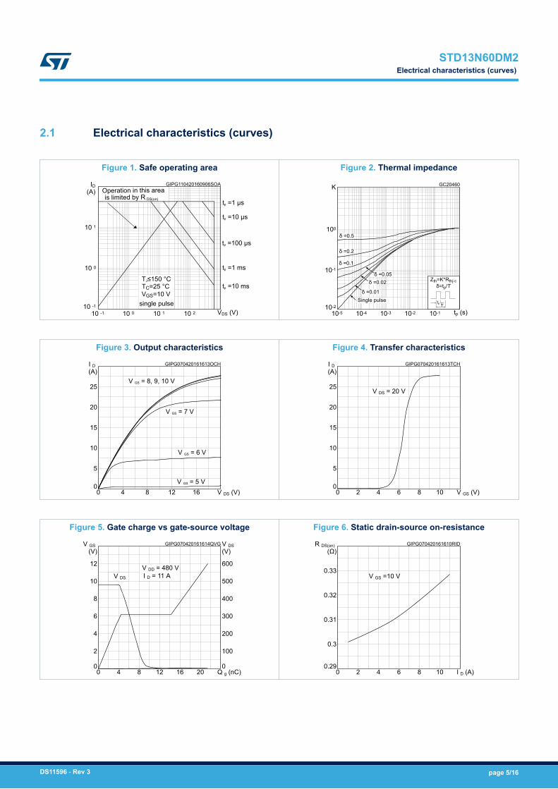
2.1 Electrical characteristics (curves)
Figure 1. Safe operating area
GIPG110420160906SOA
10 1
10 0
10 -1
10 -1 10 0 10 1 10 2
ID (A)
VDS (V)
tp =1 µs
tp =10 µs
tp =1 ms
tp =10 ms
tp =100 µs
single pulse
TJ≤150 °CTC=25 °CVGS=10 V
Operation in this areais limited by R DS(on)
Figure 2. Thermal impedance
GC20460
100
10-1
10-2
10-5 10-4 10-3 10-2 10-1
K
tp (s)
Figure 3. Output characteristics
GIPG070420161613OCH
25
20
15
10
5
00 4 8 12 16
I D (A)
V DS (V)V GS = 5 V
V GS = 8, 9, 10 V
V GS = 6 V
V GS = 7 V
Figure 4. Transfer characteristics
GIPG070420161613TCH
25
20
15
10
5
00 2 4 6 8 10
I D (A)
V GS (V)
V DS = 20 V
Figure 5. Gate charge vs gate-source voltage
GIPG070420161614QVG
12
10
8
6
4
2
0
600
500
400
300
200
100
00 4 8 12 16 20
V GS (V)
V DS (V)
Q g (nC)
V DD = 480 VI D = 11 AV DS
Figure 6. Static drain-source on-resistance
GIPG070420161610RID
0.33
0.32
0.31
0.3
0.290 2 4 6 8 10
R DS(on) (Ω)
I D (A)
V GS =10 V
STD13N60DM2Electrical characteristics (curves)
DS11596 - Rev 3 page 5/16
Figure 7. Capacitance variations
GIPG070420161612CVR
10 3
10 2
10 1
10 0
10 -110 -1 10 0 10 1 10 2
C (pF)
V DS (V)
C ISS
C OSS
C RSSf = 1 MHz
Figure 8. Normalized gate threshold voltage vstemperature
GIPG060420161230VTH
1.1
1.0
0.9
0.8
0.7
0.6-75 -25 25 75 125
V GS(th) (norm.)
T j (°C)
I D = 250 µA
Figure 9. Normalized on-resistance vs temperature
GIPG070420161233RON
2.2
1.8
1.4
1.0
0.6
0.2-75 -25 25 75 125
R DS(on) (norm.)
T j (°C)
V GS = 10 V
Figure 10. Normalized V(BR)DSS vs temperature
GIPG060420161354BDV
1.08
1.04
1.00
0.96
0.92
0.88-75 -25 25 75 125
V (BR)DSS (norm.)
T j (°C)
I D = 1 mA
Figure 11. Output capacitance stored energy
GIPG070420161614EOS
5
4
3
2
1
00 100 200 300 400 500 600
E OSS (µJ)
V DS (V)
Figure 12. Source- drain diode forward characteristics
GIPG070420161612SDF
1.1
1.0
0.9
0.8
0.7
0.6
0.50 2 4 6 8 10
V SD (V)
I SD (A)
T j = -50 °C
T j = 150 °C
T j = 25 °C
STD13N60DM2Electrical characteristics (curves)
DS11596 - Rev 3 page 6/16
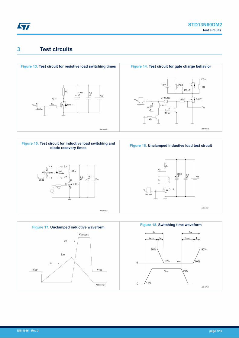
3 Test circuits
Figure 13. Test circuit for resistive load switching times
AM01468v1
VD
RG
RL
D.U.T.
2200μF VDD
3.3μF+
pulse width
VGS
Figure 14. Test circuit for gate charge behavior
AM01469v1
47 kΩ1 kΩ
47 kΩ
2.7 kΩ
1 kΩ
12 V
IG= CONST100 Ω
100 nF
D.U.T.
+pulse width
VGS
2200μF
VG
VDD
Figure 15. Test circuit for inductive load switching anddiode recovery times
AM01470v1
AD
D.U.T.S
B
G
25 Ω
A A
B B
RG
GD
S
100 µH
µF3.3 1000
µF VDD
D.U.T.
+
_
+
fastdiode
Figure 16. Unclamped inductive load test circuit
AM01471v1
VD
ID
D.U.T.
L
VDD+
pulse width
Vi
3.3µF
2200µF
Figure 17. Unclamped inductive waveform
AM01472v1
V(BR)DSS
VDDVDD
VD
IDM
ID
Figure 18. Switching time waveform
AM01473v1
0
VGS 90%
VDS
90%
10%
90%
10%
10%
ton
td(on) tr
0
toff
td(off) tf
STD13N60DM2Test circuits
DS11596 - Rev 3 page 7/16
4 Package information
In order to meet environmental requirements, ST offers these devices in different grades of ECOPACK®
packages, depending on their level of environmental compliance. ECOPACK® specifications, grade definitionsand product status are available at: www.st.com. ECOPACK® is an ST trademark.
STD13N60DM2Package information
DS11596 - Rev 3 page 8/16
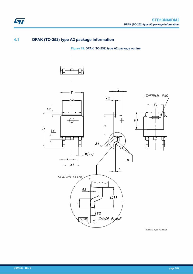
4.1 DPAK (TO-252) type A2 package information
Figure 19. DPAK (TO-252) type A2 package outline
0068772_type-A2_rev25
STD13N60DM2DPAK (TO-252) type A2 package information
DS11596 - Rev 3 page 9/16
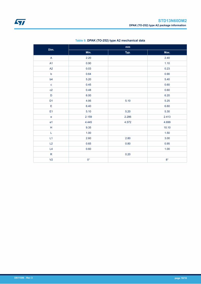
Table 9. DPAK (TO-252) type A2 mechanical data
Dim.mm
Min. Typ. Max.
A 2.20 2.40
A1 0.90 1.10
A2 0.03 0.23
b 0.64 0.90
b4 5.20 5.40
c 0.45 0.60
c2 0.48 0.60
D 6.00 6.20
D1 4.95 5.10 5.25
E 6.40 6.60
E1 5.10 5.20 5.30
e 2.159 2.286 2.413
e1 4.445 4.572 4.699
H 9.35 10.10
L 1.00 1.50
L1 2.60 2.80 3.00
L2 0.65 0.80 0.95
L4 0.60 1.00
R 0.20
V2 0° 8°
STD13N60DM2DPAK (TO-252) type A2 package information
DS11596 - Rev 3 page 10/16
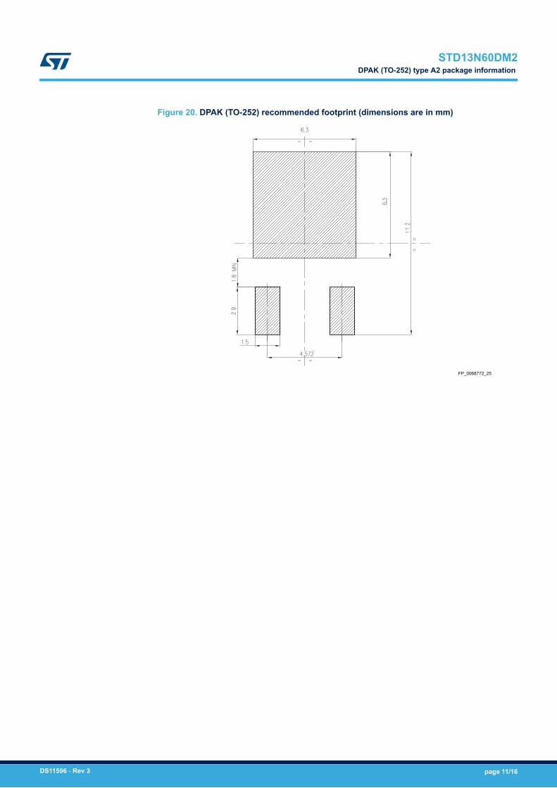
Figure 20. DPAK (TO-252) recommended footprint (dimensions are in mm)
FP_0068772_25
STD13N60DM2DPAK (TO-252) type A2 package information
DS11596 - Rev 3 page 11/16
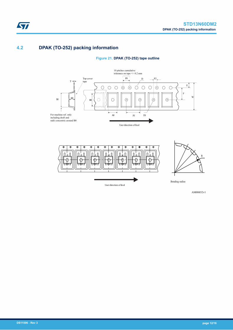
4.2 DPAK (TO-252) packing information
Figure 21. DPAK (TO-252) tape outline
P1A0 D1
P0
FW
E
D
B0K0
T
User direction of feed
P2
10 pitches cumulativetolerance on tape +/- 0.2 mm
User direction of feed
R
Bending radius
B1
For machine ref. onlyincluding draft andradii concentric around B0
AM08852v1
Top covertape
STD13N60DM2DPAK (TO-252) packing information
DS11596 - Rev 3 page 12/16
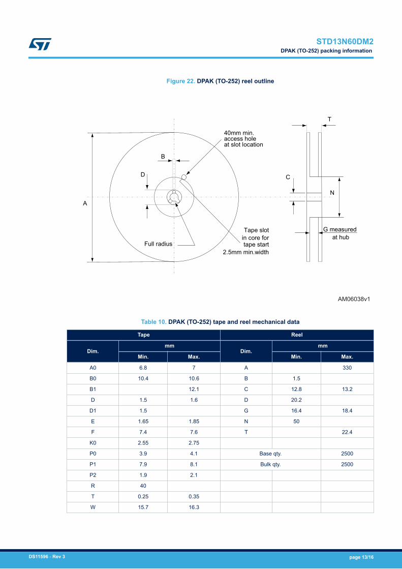
Figure 22. DPAK (TO-252) reel outline
A
D
B
Full radius
Tape slot in core for tape start
2.5mm min.width
G measured at hub
C
N
40mm min. access hole at slot location
T
AM06038v1
Table 10. DPAK (TO-252) tape and reel mechanical data
Tape Reel
Dim.mm
Dim.mm
Min. Max. Min. Max.
A0 6.8 7 A 330
B0 10.4 10.6 B 1.5
B1 12.1 C 12.8 13.2
D 1.5 1.6 D 20.2
D1 1.5 G 16.4 18.4
E 1.65 1.85 N 50
F 7.4 7.6 T 22.4
K0 2.55 2.75
P0 3.9 4.1 Base qty. 2500
P1 7.9 8.1 Bulk qty. 2500
P2 1.9 2.1
R 40
T 0.25 0.35
W 15.7 16.3
STD13N60DM2DPAK (TO-252) packing information
DS11596 - Rev 3 page 13/16
Revision history
Table 11. Document revision history
Date Revision Changes
11-Apr-2016 1 First release.
07-Dec-2016 2 Document status promoted from preliminary to production data.
29-Nov-2018 3Modified Figure 1. Safe operating area.
Minor text changes.
STD13N60DM2
DS11596 - Rev 3 page 14/16
Contents
1 Electrical ratings . . . . . . . . . . . . . . . . . . . . . . . . . . . . . . . . . . . . . . . . . . . . . . . . . . . . . . . . . . . . . . . . . .2
2 Electrical characteristics. . . . . . . . . . . . . . . . . . . . . . . . . . . . . . . . . . . . . . . . . . . . . . . . . . . . . . . . . . .3
2.1 Electrical characteristics (curves) . . . . . . . . . . . . . . . . . . . . . . . . . . . . . . . . . . . . . . . . . . . . . . . . . 5
3 Test circuits . . . . . . . . . . . . . . . . . . . . . . . . . . . . . . . . . . . . . . . . . . . . . . . . . . . . . . . . . . . . . . . . . . . . . . .7
4 Package information. . . . . . . . . . . . . . . . . . . . . . . . . . . . . . . . . . . . . . . . . . . . . . . . . . . . . . . . . . . . . . .8
4.1 DPAK (TO-252) type A2 package information . . . . . . . . . . . . . . . . . . . . . . . . . . . . . . . . . . . . . . . 8
4.2 DPAK (TO-252) packing information. . . . . . . . . . . . . . . . . . . . . . . . . . . . . . . . . . . . . . . . . . . . . . 11
Revision history . . . . . . . . . . . . . . . . . . . . . . . . . . . . . . . . . . . . . . . . . . . . . . . . . . . . . . . . . . . . . . . . . . . . . . .14
STD13N60DM2Contents
DS11596 - Rev 3 page 15/16
IMPORTANT NOTICE – PLEASE READ CAREFULLY
STMicroelectronics NV and its subsidiaries (“ST”) reserve the right to make changes, corrections, enhancements, modifications, and improvements to STproducts and/or to this document at any time without notice. Purchasers should obtain the latest relevant information on ST products before placing orders. STproducts are sold pursuant to ST’s terms and conditions of sale in place at the time of order acknowledgement.
Purchasers are solely responsible for the choice, selection, and use of ST products and ST assumes no liability for application assistance or the design ofPurchasers’ products.
No license, express or implied, to any intellectual property right is granted by ST herein.
Resale of ST products with provisions different from the information set forth herein shall void any warranty granted by ST for such product.
ST and the ST logo are trademarks of ST. All other product or service names are the property of their respective owners.
Information in this document supersedes and replaces information previously supplied in any prior versions of this document.
© 2018 STMicroelectronics – All rights reserved
STD13N60DM2
DS11596 - Rev 3 page 16/16


![Bounded Reverse Mathematicssacook/banff_survey.pdfSubsystems of Second Order Arithmetic [Sim99] Goal of Reverse Mathematics \Given a theorem ˝of ordinary mathematics, what is the](https://static.fdocument.org/doc/165x107/5f08d8bd7e708231d42401e8/bounded-reverse-mathematics-sacookbanffsurveypdf-subsystems-of-second-order-arithmetic.jpg)