
Αξιολόγηση πληροφοριακών συστημάτων και υπηρεσιών πληροφόρησης 200 5 – 200 6
1 23
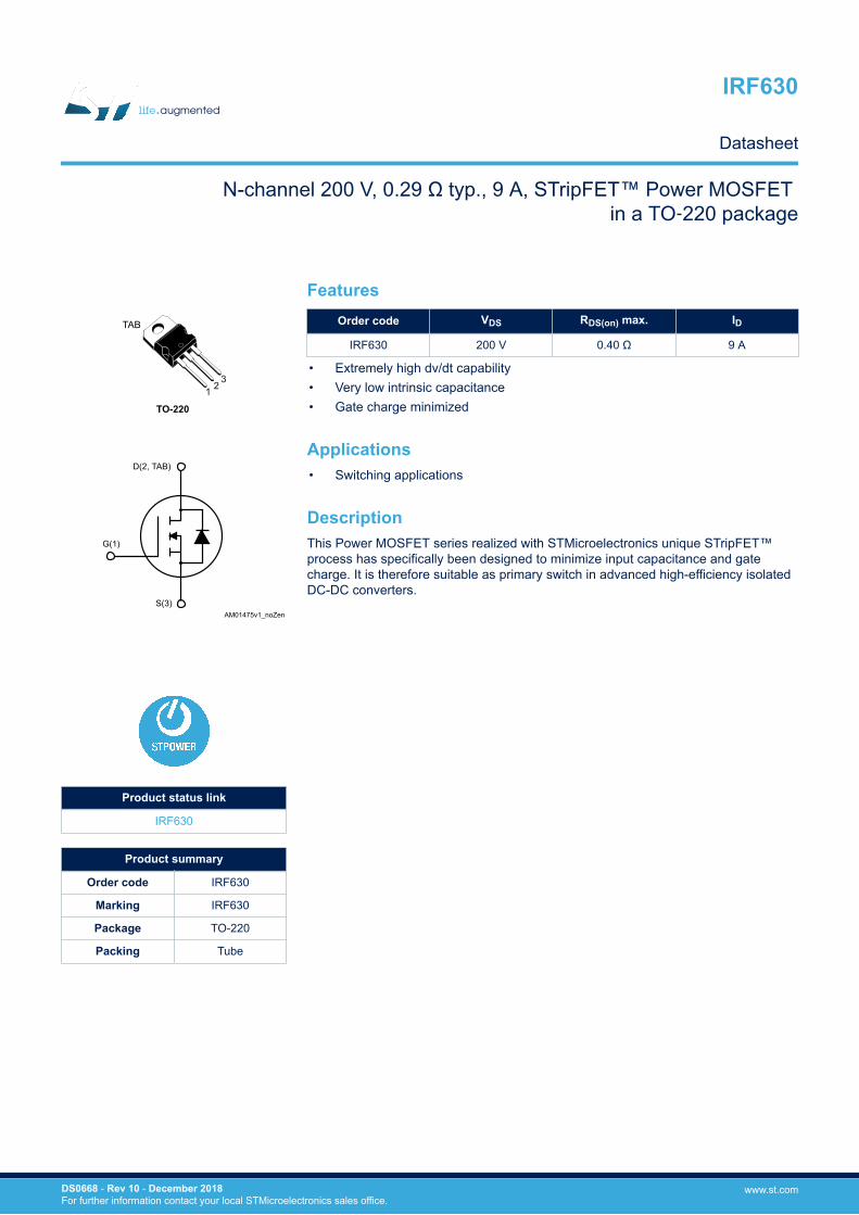
TO-220
TAB
AM01475v1_noZen
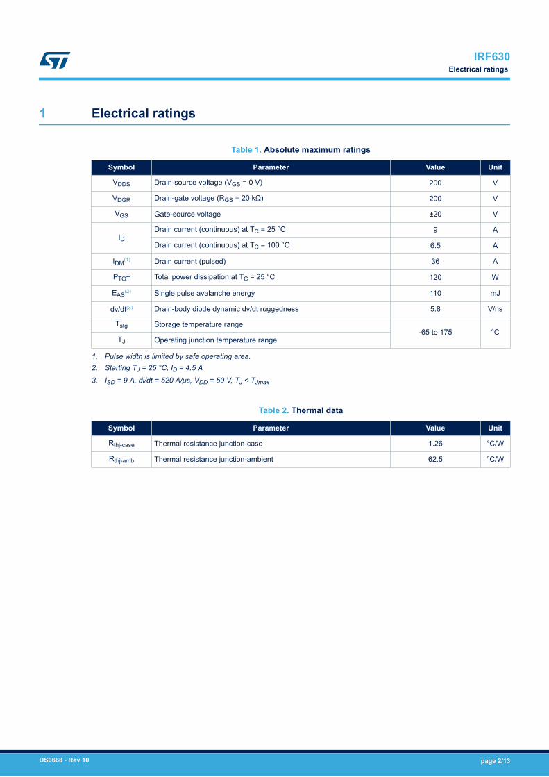
D(2, TAB)
G(1)
S(3)
FeaturesOrder code VDS RDS(on) max. ID
IRF630 200 V 0.40 Ω 9 A
• Extremely high dv/dt capability• Very low intrinsic capacitance• Gate charge minimized
Applications• Switching applications
DescriptionThis Power MOSFET series realized with STMicroelectronics unique STripFET™process has specifically been designed to minimize input capacitance and gatecharge. It is therefore suitable as primary switch in advanced high-efficiency isolatedDC-DC converters.
Product status link
IRF630
Product summary
Order code IRF630
Marking IRF630
Package TO-220
Packing Tube
N-channel 200 V, 0.29 Ω typ., 9 A, STripFET™ Power MOSFET in a TO‑220 package
IRF630
Datasheet
DS0668 - Rev 10 - December 2018For further information contact your local STMicroelectronics sales office.
www.st.com
1 Electrical ratings
Table 1. Absolute maximum ratings
Symbol Parameter Value Unit
VDDS Drain-source voltage (VGS = 0 V) 200 V
VDGR Drain-gate voltage (RGS = 20 kΩ) 200 V
VGS Gate-source voltage ±20 V
IDDrain current (continuous) at TC = 25 °C 9 A
Drain current (continuous) at TC = 100 °C 6.5 A
IDM(1) Drain current (pulsed) 36 A
PTOT Total power dissipation at TC = 25 °C 120 W
EAS(2) Single pulse avalanche energy 110 mJ
dv/dt(3) Drain-body diode dynamic dv/dt ruggedness 5.8 V/ns
Tstg Storage temperature range-65 to 175 °C
TJ Operating junction temperature range
1. Pulse width is limited by safe operating area.2. Starting TJ = 25 °C, ID = 4.5 A
3. ISD = 9 A, di/dt = 520 A/μs, VDD = 50 V, TJ < TJmax
Table 2. Thermal data
Symbol Parameter Value Unit
Rthj-case Thermal resistance junction-case 1.26 °C/W
Rthj-amb Thermal resistance junction-ambient 62.5 °C/W
IRF630Electrical ratings
DS0668 - Rev 10 page 2/13
2 Electrical characteristics
TCASE = 25 °C unless otherwise specified
Table 3. On/off states
Symbol Parameter Test conditions Min. Typ. Max. Unit
V(BR)DSS Drain-source breakdown voltage VGS = 0 V, ID = 250 μA 200 V
IDSS Zero gate voltage drain current
VGS = 0 V, VDS = 200 V 1 µA
VGS = 0 V, VDS = 200 V,
TC = 125 °C(1)100 µA
IGSS Gate body leakage current VDS = 0 V, VGS = 20 V ±100 nA
VGS(th) Gate threshold voltage VDS = VGS, ID = 250 µA 2 3 4 V
RDS(on) Static drain-source on-resistance VGS = 10 V, ID = 4.5 A 0.29 0.40 Ω
1. Defined by design, not subject to production test.
Table 4. Dynamic
Symbol Parameter Test conditions Min. Typ. Max. Unit
Ciss Input capacitanceVDS = 25 V, f = 1 MHz,
VGS = 0 V
- 370 - pF
Coss Output capacitance - 77 - pF
Crss Reverse transfer capacitance - 14 - pF
Qg Total gate charge VDD = 160 V, ID = 9 A
VGS = 0 to 10 V
(see Figure 13. Test circuit for gatecharge behavior)
- 11.6 - nC
Qgs Gate-source charge - 2.2 - nC
Qgd Gate-drain charge - 5.5 - nC
Table 5. Switching times
Symbol Parameter Test conditions Min. Typ. Max. Unit
td(on) Turn-on delay time VDD = 100 V, ID = 4.5 A,
RG = 4.7 Ω, VGS = 10 V
(see Figure 12. Test circuit forresistive load switching times andFigure 17. Switching timewaveform)
- 5.6 - ns
tr Rise time - 2.6 - ns
IRF630Electrical characteristics
DS0668 - Rev 10 page 3/13
Table 6. Source-drain diode
Symbol Parameter Test conditions Min. Typ. Max. Unit
VSD(1) Forward on voltage ISD = 9 A, VGS = 0 V - 1.5 V
trr Reverse recovery time ISD = 9 A, di/dt = 100 A/µs,
VDD = 50 V
(see Figure 17. Switching timewaveform)
- 118.5 ns
Qrr Reverse recovery charge - 393 nC
IRRM Reverse recovery current - 6.6 A
1. Pulsed: pulse duration = 300 µs, duty cycle 1.5%
IRF630Electrical characteristics
DS0668 - Rev 10 page 4/13
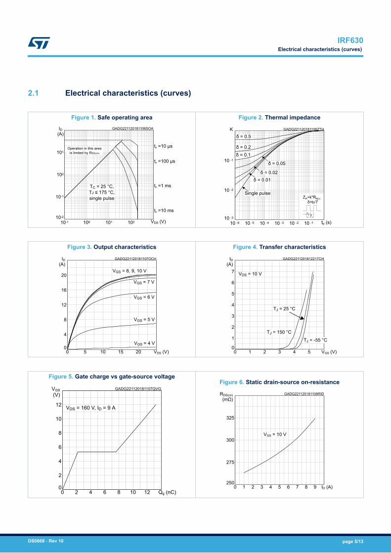
2.1 Electrical characteristics (curves)
Figure 1. Safe operating areaGADG221120181106SOA
101
100
10-1
10-2
10-1 100 101 102
ID (A)
VDS (V)
tp =10 µs
tp =100 µs
tp =1 ms
tp =10 ms
Operation in this areais limited by RDS(on)
TC = 25 °C,TJ ≤ 175 °C,single pulse
Figure 2. Thermal impedance
GADG221120181106ZTH
10 -1
10 -2
10 -3
10 -6 10 -5 10 -4 10 -3 10 -2 10 -1
K
tp (s)
δ = 0.5
δ = 0.1
δ = 0.05
δ = 0.02δ = 0.01
Single pulse
δ = 0.2
Figure 3. Output characteristics
GADG221120181107OCH
20
16
12
8
4
00 5 10 15 20
ID (A)
VDS (V)
VGS = 8, 9, 10 V
VGS = 7 V
VGS = 6 V
VGS = 5 V
VGS = 4 V
Figure 4. Transfer characteristics
GADG221120181221TCH
7
6
5
4
3
2
1
00 1 2 3 4 5
ID (A)
VGS (V)
VDS = 10 V
TJ = 25 °C
TJ = 150 °CTJ = -55 °C
Figure 5. Gate charge vs gate-source voltage
GADG221120181107QVG
12
10
8
6
4
2
00 2 4 6 8 10 12
VGS (V)
Qg (nC)
VDS = 160 V, ID = 9 A
Figure 6. Static drain-source on-resistance
GADG221120181108RID
325
300
275
2500 1 2 3 4 5 6 7 8 9
RDS(on) (mΩ)
ID (A)
VGS = 10 V
IRF630Electrical characteristics (curves)
DS0668 - Rev 10 page 5/13
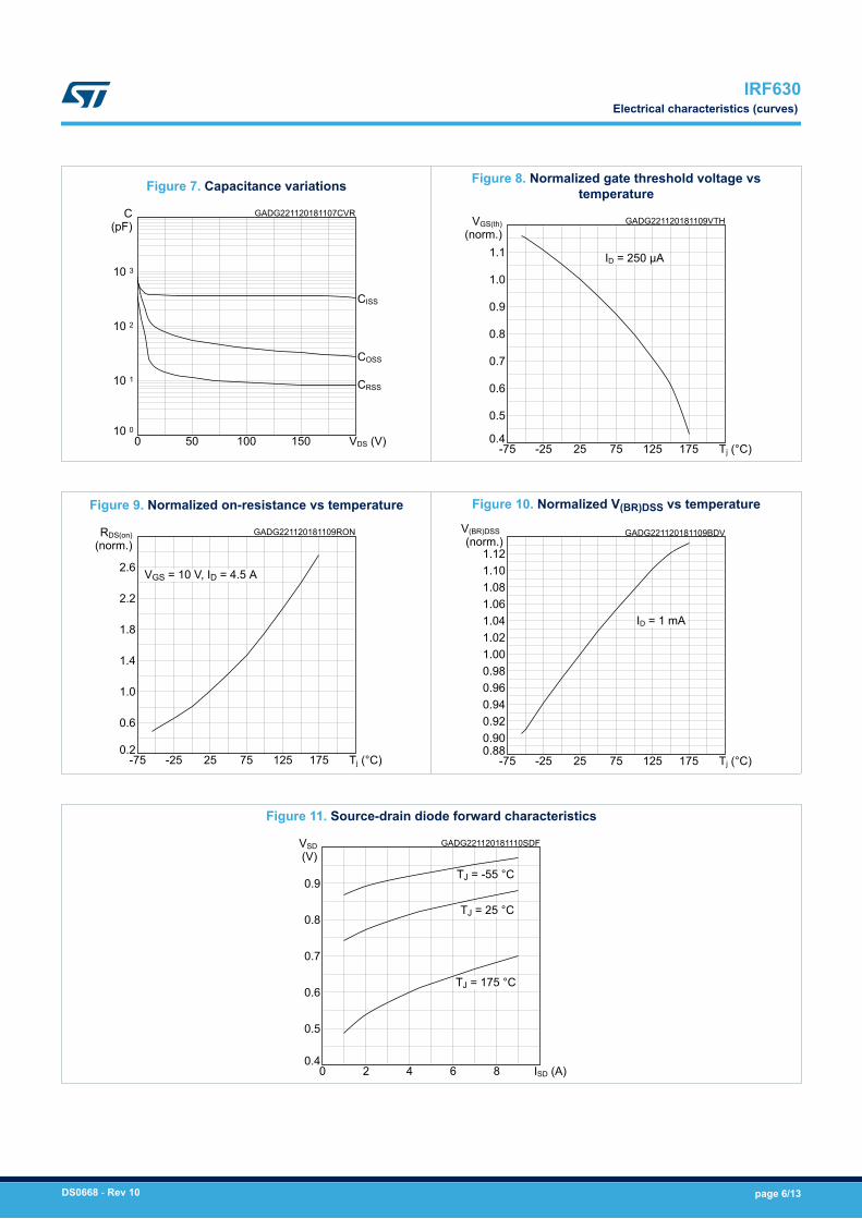
Figure 7. Capacitance variations
GADG221120181107CVR
10 3
10 2
10 1
10 0 0 50 100 150
C (pF)
VDS (V)
CISS
COSS
CRSS
Figure 8. Normalized gate threshold voltage vstemperature
GADG221120181109VTH
1.1
1.0
0.9
0.8
0.7
0.6
0.5
0.4-75 -25 25 75 125 175
VGS(th) (norm.)
Tj (°C)
ID = 250 µA
Figure 9. Normalized on-resistance vs temperature
GADG221120181109RON
2.6
2.2
1.8
1.4
1.0
0.6
0.2-75 -25 25 75 125 175
RDS(on) (norm.)
Tj (°C)
VGS = 10 V, ID = 4.5 A
Figure 10. Normalized V(BR)DSS vs temperature
GADG221120181109BDV
1.121.101.081.061.041.021.000.980.960.940.920.900.88
-75 -25 25 75 125 175
V(BR)DSS (norm.)
Tj (°C)
ID = 1 mA
Figure 11. Source-drain diode forward characteristics
GADG221120181110SDF
0.9
0.8
0.7
0.6
0.5
0.40 2 4 6 8
VSD (V)
ISD (A)
TJ = 175 °C
TJ = 25 °C
TJ = -55 °C
IRF630Electrical characteristics (curves)
DS0668 - Rev 10 page 6/13
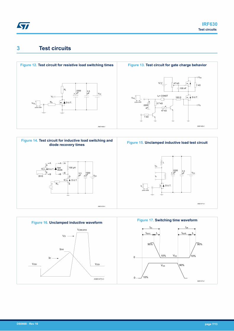
3 Test circuits
Figure 12. Test circuit for resistive load switching times
AM01468v1
VD
RG
RL
D.U.T.
2200μF VDD
3.3μF+
pulse width
VGS
Figure 13. Test circuit for gate charge behavior
AM01469v1
47 kΩ1 kΩ
47 kΩ
2.7 kΩ
1 kΩ
12 V
IG= CONST100 Ω
100 nF
D.U.T.
+pulse width
VGS
2200μF
VG
VDD
Figure 14. Test circuit for inductive load switching anddiode recovery times
AM01470v1
AD
D.U.T.S
B
G
25 Ω
A A
B B
RG
GD
S
100 µH
µF3.3 1000
µF VDD
D.U.T.
+
_
+
fastdiode
Figure 15. Unclamped inductive load test circuit
AM01471v1
VD
ID
D.U.T.
L
VDD+
pulse width
Vi
3.3µF
2200µF
Figure 16. Unclamped inductive waveform
AM01472v1
V(BR)DSS
VDDVDD
VD
IDM
ID
Figure 17. Switching time waveform
AM01473v1
0
VGS 90%
VDS
90%
10%
90%
10%
10%
ton
td(on) tr
0
toff
td(off) tf
IRF630Test circuits
DS0668 - Rev 10 page 7/13
4 Package information
In order to meet environmental requirements, ST offers these devices in different grades of ECOPACK®
packages, depending on their level of environmental compliance. ECOPACK® specifications, grade definitionsand product status are available at: www.st.com. ECOPACK® is an ST trademark.
IRF630Package information
DS0668 - Rev 10 page 8/13
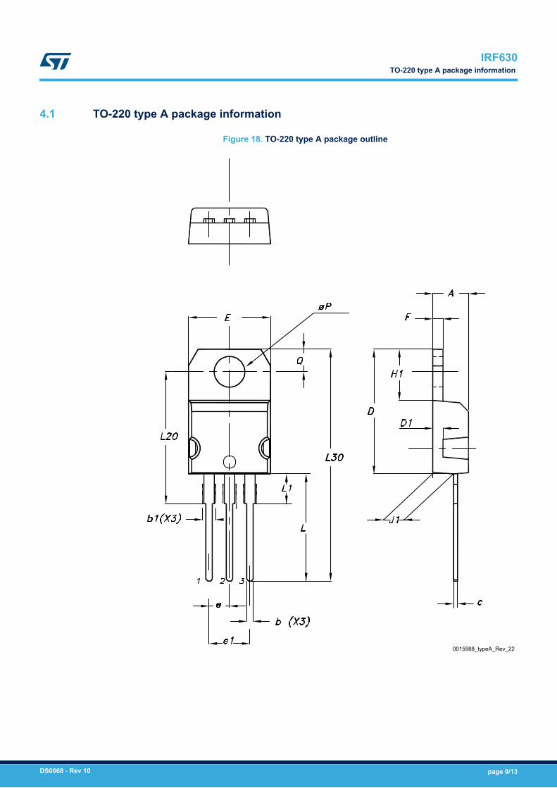
4.1 TO-220 type A package information
Figure 18. TO-220 type A package outline
0015988_typeA_Rev_22
IRF630TO-220 type A package information
DS0668 - Rev 10 page 9/13
Table 7. TO-220 type A package mechanical data
Dim.mm
Min. Typ. Max.
A 4.40 4.60
b 0.61 0.88
b1 1.14 1.55
c 0.48 0.70
D 15.25 15.75
D1 1.27
E 10.00 10.40
e 2.40 2.70
e1 4.95 5.15
F 1.23 1.32
H1 6.20 6.60
J1 2.40 2.72
L 13.00 14.00
L1 3.50 3.93
L20 16.40
L30 28.90
øP 3.75 3.85
Q 2.65 2.95
IRF630TO-220 type A package information
DS0668 - Rev 10 page 10/13
Revision history
Table 8. Document revision history
Date Version Changes
09-Sep-2004 8 Complete version
03-Aug-2006 9 New template, no content change
12-Dec-2018 10Part number IRF630FP has been moved to a separate datasheet and thedocument has been updated accordingly.
Minor text changes
IRF630
DS0668 - Rev 10 page 11/13
Contents
1 Electrical ratings . . . . . . . . . . . . . . . . . . . . . . . . . . . . . . . . . . . . . . . . . . . . . . . . . . . . . . . . . . . . . . . . . .2
2 Electrical characteristics. . . . . . . . . . . . . . . . . . . . . . . . . . . . . . . . . . . . . . . . . . . . . . . . . . . . . . . . . . .3
2.1 Electrical characteristics (curves) . . . . . . . . . . . . . . . . . . . . . . . . . . . . . . . . . . . . . . . . . . . . . . . . . 5
3 Test circuits . . . . . . . . . . . . . . . . . . . . . . . . . . . . . . . . . . . . . . . . . . . . . . . . . . . . . . . . . . . . . . . . . . . . . . .7
4 Package information. . . . . . . . . . . . . . . . . . . . . . . . . . . . . . . . . . . . . . . . . . . . . . . . . . . . . . . . . . . . . . .8
4.1 TO-220 type A package information . . . . . . . . . . . . . . . . . . . . . . . . . . . . . . . . . . . . . . . . . . . . . . . 8
Revision history . . . . . . . . . . . . . . . . . . . . . . . . . . . . . . . . . . . . . . . . . . . . . . . . . . . . . . . . . . . . . . . . . . . . . . .11
IRF630Contents
DS0668 - Rev 10 page 12/13
IMPORTANT NOTICE – PLEASE READ CAREFULLY
STMicroelectronics NV and its subsidiaries (“ST”) reserve the right to make changes, corrections, enhancements, modifications, and improvements to STproducts and/or to this document at any time without notice. Purchasers should obtain the latest relevant information on ST products before placing orders. STproducts are sold pursuant to ST’s terms and conditions of sale in place at the time of order acknowledgement.
Purchasers are solely responsible for the choice, selection, and use of ST products and ST assumes no liability for application assistance or the design ofPurchasers’ products.
No license, express or implied, to any intellectual property right is granted by ST herein.
Resale of ST products with provisions different from the information set forth herein shall void any warranty granted by ST for such product.
ST and the ST logo are trademarks of ST. All other product or service names are the property of their respective owners.
Information in this document supersedes and replaces information previously supplied in any prior versions of this document.
© 2018 STMicroelectronics – All rights reserved
IRF630
DS0668 - Rev 10 page 13/13


![LABORATÓRIO DE SISTEMAS MECATRÔNICOS E ROBÓTICA ] - LAB.pdf · Resistores - 1,0 Ω - 100k Ω 1,2 Ω - 120k Ω 1,5 Ω - 150k Ω 1,8 Ω- 180k Ω 2,2 Ω– 220k Ω 2,7 Ω– 270k](https://static.fdocument.org/doc/165x107/5c245c1a09d3f224508c4b48/laboratorio-de-sistemas-mecatronicos-e-robotica-labpdf-resistores-.jpg)