DATASHEET AND OPERATING GUIDE FL591FL · MON1 Parallel 500 μA / V 1 When operating the FL591FL as...
18
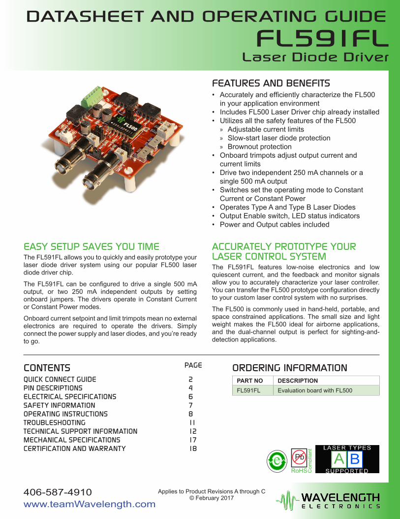
ORDERING INFORMATION PART NO DESCRIPTION FL591FL Evaluation board with FL500 EASY SETUP SAVES YOU TIME The FL591FL allows you to quickly and easily prototype your laser diode driver system using our popular FL500 laser diode driver chip. The FL591FL can be configured to drive a single 500 mA output, or two 250 mA independent outputs by setting onboard jumpers. The drivers operate in Constant Current or Constant Power modes. Onboard current setpoint and limit trimpots mean no external electronics are required to operate the drivers. Simply connect the power supply and laser diodes, and you’re ready to go. ACCURATELY PROTOTYPE YOUR LASER CONTROL SYSTEM The FL591FL features low-noise electronics and low quiescent current, and the feedback and monitor signals allow you to accurately characterize your laser controller. You can transfer the FL500 prototype configuration directly to your custom laser control system with no surprises. The FL500 is commonly used in hand-held, portable, and space constrained applications. The small size and light weight makes the FL500 ideal for airborne applications, and the dual-channel output is perfect for sighting-and- detection applications. FEATURES AND BENEFITS • Accurately and efficiently characterize the FL500 in your application environment • Includes FL500 Laser Driver chip already installed • Utilizes all the safety features of the FL500 » Adjustable current limits » Slow-start laser diode protection » Brownout protection • Onboard trimpots adjust output current and current limits • Drive two independent 250 mA channels or a single 500 mA output • Switches set the operating mode to Constant Current or Constant Power • Operates Type A and Type B Laser Diodes • Output Enable switch, LED status indicators • Power and Output cables included CONTENTS QUICK CONNECT GUIDE 2 PIN DESCRIPTIONS 4 ELECTRICAL SPECIFICATIONS 6 SAFETY INFORMATION 7 OPERATING INSTRUCTIONS 8 TROUBLESHOOTING 11 TECHNICAL SUPPORT INFORMATION 12 MECHANICAL SPECIFICATIONS 17 CERTIFICATION AND WARRANTY 18 e Pb RoHS Compliant PAGE Applies to Product Revisions A through C © February 2017 406-587-4910 www.teamWavelength.com FL591FL Laser Diode Driver DATASHEET AND OPERATING GUIDE
Transcript of DATASHEET AND OPERATING GUIDE FL591FL · MON1 Parallel 500 μA / V 1 When operating the FL591FL as...
ORDERING INFORMATIONPART NO DESCRIPTIONFL591FL Evaluation board with FL500
EASY SETUP SAVES YOU TIMEThe FL591FL allows you to quickly and easily prototype your laser diode driver system using our popular FL500 laser diode driver chip.
The FL591FL can be configured to drive a single 500 mA output, or two 250 mA independent outputs by setting onboard jumpers. The drivers operate in Constant Current or Constant Power modes.
Onboard current setpoint and limit trimpots mean no external electronics are required to operate the drivers. Simply connect the power supply and laser diodes, and you’re ready to go.
ACCURATELY PROTOTYPE YOUR LASER CONTROL SYSTEMThe FL591FL features low-noise electronics and low quiescent current, and the feedback and monitor signals allow you to accurately characterize your laser controller. You can transfer the FL500 prototype configuration directly to your custom laser control system with no surprises.
The FL500 is commonly used in hand-held, portable, and space constrained applications. The small size and light weight makes the FL500 ideal for airborne applications, and the dual-channel output is perfect for sighting-and-detection applications.
FEATURES AND BENEFITS• Accurately and efficiently characterize the FL500
in your application environment• Includes FL500 Laser Driver chip already installed• Utilizes all the safety features of the FL500
» Adjustable current limits » Slow-start laser diode protection » Brownout protection
• Onboard trimpots adjust output current and current limits
• Drive two independent 250 mA channels or a single 500 mA output
• Switches set the operating mode to Constant Current or Constant Power
• Operates Type A and Type B Laser Diodes• Output Enable switch, LED status indicators• Power and Output cables included
CONTENTSQUICK CONNECT GUIDE 2PIN DESCRIPTIONS 4ELECTRICAL SPECIFICATIONS 6SAFETY INFORMATION 7OPERATING INSTRUCTIONS 8TROUBLESHOOTING 11TECHNICAL SUPPORT INFORMATION 12MECHANICAL SPECIFICATIONS 17CERTIFICATION AND WARRANTY 18
e Pb
RoHS Com
plia
nt
PAGE
Applies to Product Revisions A through C© February 2017
406-587-4910www.teamWavelength.com
FL591FLLaser Diode Driver
DATASHEET AND OPERATING GUIDE
© 2017 www.teamWavelength.com 2
FL591FL LASER DIODE DRIVER
QUICK CONNECT GUIDE
!It Is ImperatIve that you verIfy the unIt wIll operate wIthIn the Internal heat dIssIpatIon safe operatIng area (soa).
operatIng the drIver outsIde the soa may damage or destroy the drIver and/or laser.
Visit the Wavelength Electronics website for the most accurate, up-to-date, and easy to use SOA calculator:
http://www.teamwavelength.com/support/calculator/soa/soald.php
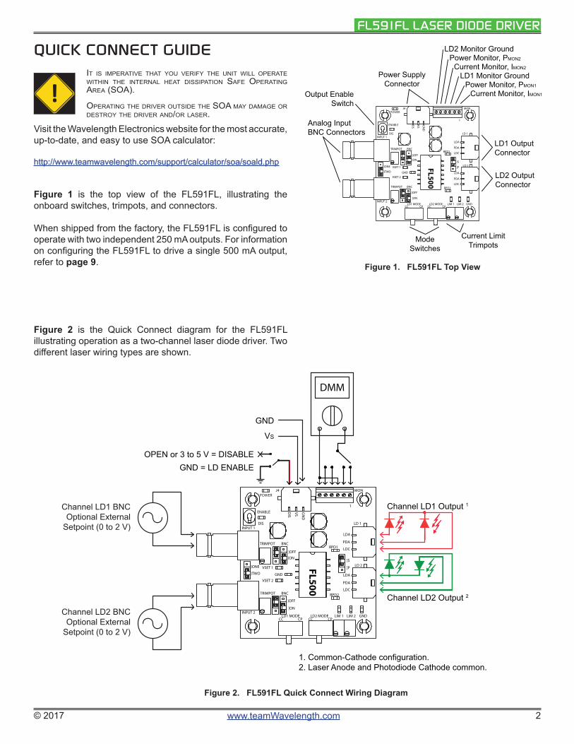
Figure 1 is the top view of the FL591FL, illustrating the onboard switches, trimpots, and connectors.
When shipped from the factory, the FL591FL is configured to operate with two independent 250 mA outputs. For information on configuring the FL591FL to drive a single 500 mA output, refer to page 9.
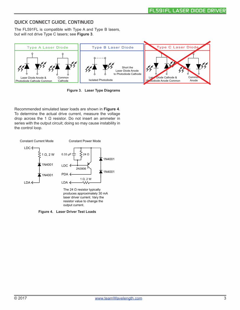
Figure 2 is the Quick Connect diagram for the FL591FL illustrating operation as a two-channel laser diode driver. Two different laser wiring types are shown.
Current Monitor, IMON1
Power Monitor, PMON1
LD1 Monitor GroundCurrent Monitor, IMON2
Power Monitor, PMON2
LD2 Monitor Ground
LD1 OutputConnector
LD2 OutputConnector
ModeSwitches
Current LimitTrimpots
Power SupplyConnector
Analog InputBNC Connectors
Output EnableSwitch
ENABLE
DISINPUT 1
INPUT 2
TRIMPOT
TRIMPOT
BNC
BNC
VSET 1
VSET 2GND
GNDLD1 MODECC CP CPCC
LD2 MODE LIM 1 LIM 2
LDA
LDA
PDA
PDA
LDC
LDC
LD 1
MON
1
DS
VS GN
D
]ON
]OFF
]ONE
]TWO
]OFF
]ON
LD 2]S
]P
POWER
RPD1
RPD2
FL500
J4
Figure 1. FL591FL Top View
Figure 2. FL591FL Quick Connect Wiring Diagram
Channel LD1 Output 1Channel LD1 BNCOptional External
Setpoint (0 to 2 V)
Channel LD2 BNCOptional External
Setpoint (0 to 2 V)
OPEN or 3 to 5 V = DISABLEGND = LD ENABLE
GND
VS
DMM
ENABLE
DISINPUT 1
INPUT 2
TRIMPOT
TRIMPOT
BNC
BNC
VSET 1
VSET 2GND
GNDLD1 MODECC CP CPCC
LD2 MODE LIM 1 LIM 2
LDA
LDA
PDA
PDA
LDC
LDC
LD 1
MON
1
DIS
VS GN
D
]ON
]OFF
]ONE
]TWO
]OFF
]ON
LD 2]S
]P
1. Common-Cathode configuration.2. Laser Anode and Photodiode Cathode common.
Channel LD2 Output 2
POWER
RPD1
RPD2
FL500
J4
© 2017 www.teamWavelength.com 3
FL591FL LASER DIODE DRIVER
QUICK CONNECT GUIDE, CONTINUED
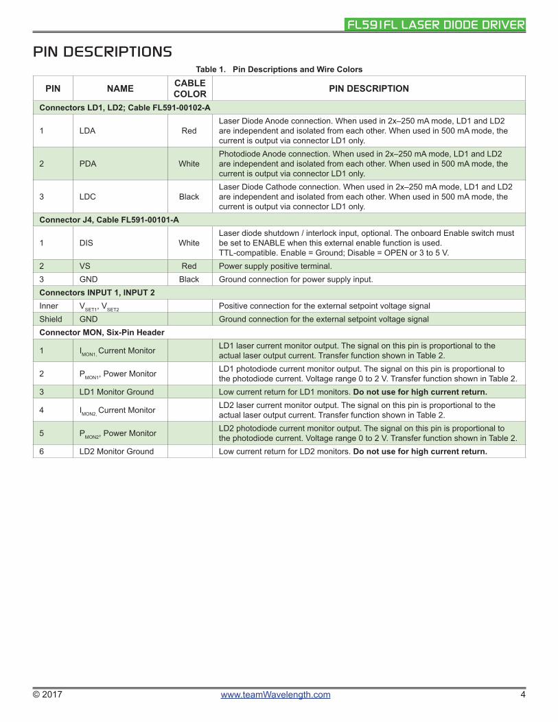
The FL591FL is compatible with Type A and Type B lasers, but will not drive Type C lasers; see Figure 3.
Type A Laser Diode Type B Laser Diode Type C Laser Diode
CommonCathode
Laser Diode Anode & Photodiode Cathode Common Isolated Photodiode
Short theLaser Diode Anode
to Photodiode CathodeCommon
AnodeLaser Diode Cathode &
Photodiode Anode Common
Figure 3. Laser Type Diagrams
Recommended simulated laser loads are shown in Figure 4. To determine the actual drive current, measure the voltage drop across the 1 Ω resistor. Do not insert an ammeter in series with the output circuit; doing so may cause instability in the control loop.
24 Ω
1N4001
1N40012N3906
0.33 µF
PDA
LDA
LDC1N4001
1N4001
LDC
LDA
1 Ω, 2 W
Constant Current Mode Constant Power Mode
The 24 Ω resistor typically produces approximately 30 mA laser driver current. Vary the resistor value to change the output current.
1 Ω, 2 W
Figure 4. Laser Driver Test Loads
© 2017 www.teamWavelength.com 4
FL591FL LASER DIODE DRIVER
PIN DESCRIPTIONSTable 1. Pin Descriptions and Wire Colors
PIN NAME CABLE COLOR PIN DESCRIPTION
Connectors LD1, LD2; Cable FL591-00102-A
1 LDA RedLaser Diode Anode connection. When used in 2x–250 mA mode, LD1 and LD2 are independent and isolated from each other. When used in 500 mA mode, the current is output via connector LD1 only.
2 PDA WhitePhotodiode Anode connection. When used in 2x–250 mA mode, LD1 and LD2 are independent and isolated from each other. When used in 500 mA mode, the current is output via connector LD1 only.
3 LDC BlackLaser Diode Cathode connection. When used in 2x–250 mA mode, LD1 and LD2 are independent and isolated from each other. When used in 500 mA mode, the current is output via connector LD1 only.
Connector J4, Cable FL591-00101-A
1 DIS WhiteLaser diode shutdown / interlock input, optional. The onboard Enable switch must be set to ENABLE when this external enable function is used. TTL-compatible. Enable = Ground; Disable = OPEN or 3 to 5 V.
2 VS Red Power supply positive terminal.3 GND Black Ground connection for power supply input.Connectors INPUT 1, INPUT 2Inner VSET1, VSET2 Positive connection for the external setpoint voltage signalShield GND Ground connection for the external setpoint voltage signalConnector MON, Six-Pin Header
1 IMON1, Current Monitor LD1 laser current monitor output. The signal on this pin is proportional to the actual laser output current. Transfer function shown in Table 2.
2 PMON1, Power Monitor LD1 photodiode current monitor output. The signal on this pin is proportional to the photodiode current. Voltage range 0 to 2 V. Transfer function shown in Table 2.
3 LD1 Monitor Ground Low current return for LD1 monitors. Do not use for high current return.
4 IMON2, Current Monitor LD2 laser current monitor output. The signal on this pin is proportional to the actual laser output current. Transfer function shown in Table 2.
5 PMON2, Power Monitor LD2 photodiode current monitor output. The signal on this pin is proportional to the photodiode current. Voltage range 0 to 2 V. Transfer function shown in Table 2.
6 LD2 Monitor Ground Low current return for LD2 monitors. Do not use for high current return.
© 2017 www.teamWavelength.com 5
FL591FL LASER DIODE DRIVER
Table 2. Monitor Transfer Functions
FUNCTION OUTPUT CONFIGURATION TRANSFER NOTE
Current Output Monitor, IMON1 and IMON2
Separate 0.125 A / V The voltage on IMONx is proportional to the current output on that channel
Current Output Monitor, IMON1 + IMON2
Parallel
When operating the FL591FL as a single channel 500 mA driver, monitor the output current on both IMON1 and IMON2. The total output current monitor voltage is determined by summing the voltage measured on both monitors, using the equation: ILD = (VIMON1 + VIMON2) * 0.125
Current Limit Monitor, ILIM1 and ILIM2
Separate 0.125 A / V Adjust ILIM1 and ILIM2 to set the current limit on each channel. See page 9.
Current Limit Monitor, ILIM1 Parallel 0.250 A / VAdjust only ILIM1 to set the current limit when the FL591FL is operated in parallel-output mode. See page 9.
Power Monitor, PMON1 and PMON2
Separate 500 μA / V 1 The voltage on PMONx is proportional to the photodiode current on that channel.
Power Monitor, PMON1 Parallel 500 μA / V 1When operating the FL591FL as a single channel 500 mA driver, the photodiode current is monitored on PMON1.
1. The photodiode feedback transfer function can be changed. See page 12 for details.
Table 3. Setpoint Transfer FunctionsOPERATING
MODEINPUT
CONFIG.OUTPUT CONFIG.
VSET TRANSFER FUNCTION NOTES
Constant Current
One
Separate 0.125 A / VMeasure the voltage on the VSET1 testpoint; adjust the VSET1 trimpot to set the output current on both channels. The VSET2 trimpot is not used.
Parallel 0.250 A / VMeasure the voltage on the VSET1 testpoint; adjust the VSET1 trimpot to set the output current on both channels. The VSET2 trimpot is not used.
Two
Separate 0.125 A / VMeasure the voltage on the VSET1 and VSET2 testpoints; adjust the VSET1 and VSET2 trimpots to set the output current level for each channel.
Parallel 0.125 A / V
The VSET1 and VSET2 voltages drive each channel independently. The output currents sum. Measure the voltages on the VSET1 and VSET2 testpoints separately, and add them to determine the effective output current.
Constant Power
One
Separate 500 μA / V 1Measure the voltage on the VSET1 testpoint; adjust the VSET1 trimpot to set the photodiode current setpoint. The VSET2 trimpot is not used.
Parallel 500 μA / V 1Measure the voltage on the VSET1 testpoint; adjust the VSET1 trimpot to set the photodiode current setpoint. The VSET2 trimpot is not used.
TwoSeparate 500 μA / V 1
Measure the voltage on the VSET1 and VSET2 testpoints; adjust the VSET1 and VSET2 trimpots to set the photodiode setpoint for each channel.
Parallel __ This configuration is not allowed.
1. The photodiode feedback transfer function can be changed. See page 12 for details.
© 2017 www.teamWavelength.com 6
FL591FL LASER DIODE DRIVER
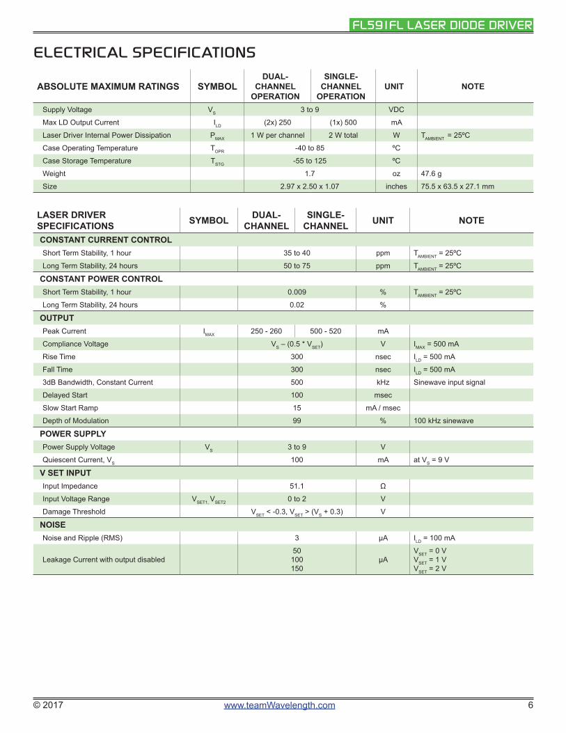
ELECTRICAL SPECIFICATIONS
ABSOLUTE MAXIMUM RATINGS SYMBOLDUAL-
CHANNEL OPERATION
SINGLE-CHANNEL
OPERATIONUNIT NOTE
Supply Voltage VS 3 to 9 VDC
Max LD Output Current ILD (2x) 250 (1x) 500 mA
Laser Driver Internal Power Dissipation PMAX 1 W per channel 2 W total W TAMBIENT = 25ºC
Case Operating Temperature TOPR -40 to 85 ºC
Case Storage Temperature TSTG -55 to 125 ºC
Weight 1.7 oz 47.6 g
Size 2.97 x 2.50 x 1.07 inches 75.5 x 63.5 x 27.1 mm
LASER DRIVER SPECIFICATIONS SYMBOL DUAL-
CHANNELSINGLE-
CHANNEL UNIT NOTE
CONSTANT CURRENT CONTROLShort Term Stability, 1 hour 35 to 40 ppm TAMBIENT = 25ºC
Long Term Stability, 24 hours 50 to 75 ppm TAMBIENT = 25ºC
CONSTANT POWER CONTROLShort Term Stability, 1 hour 0.009 % TAMBIENT = 25ºC
Long Term Stability, 24 hours 0.02 %
OUTPUTPeak Current IMAX 250 - 260 500 - 520 mA
Compliance Voltage VS – (0.5 * VSET) V IMAX = 500 mA
Rise Time 300 nsec ILD = 500 mA
Fall Time 300 nsec ILD = 500 mA
3dB Bandwidth, Constant Current 500 kHz Sinewave input signal
Delayed Start 100 msec
Slow Start Ramp 15 mA / msec
Depth of Modulation 99 % 100 kHz sinewave
POWER SUPPLYPower Supply Voltage VS 3 to 9 V
Quiescent Current, VS 100 mA at VS = 9 V
V SET INPUTInput Impedance 51.1 Ω
Input Voltage Range VSET1, VSET2 0 to 2 V
Damage Threshold VSET < -0.3, VSET > (VS + 0.3) V
NOISENoise and Ripple (RMS) 3 µA ILD = 100 mA
Leakage Current with output disabled50
100150
µAVSET = 0 VVSET = 1 VVSET = 2 V
© 2017 www.teamWavelength.com 7
FL591FL LASER DIODE DRIVER
THEORY OF OPERATIONThe FL591FL employs Wavelength’s FL500 laser diode control chip, and can drive a single output up to 500 mA or dual outputs up to 250 mA each.
When operating with two separate outputs, the FL591FL can be configured to use a single setpoint to drive both outputs to the same current, or use separate setpoint signals to drive each current source independently.
It may be useful to remember that you do not directly set the drive current setpoint; instead, you adjust a voltage signal that represents the output current. The setpoint voltage is controlled by the onboard trimpot or by an external input.
The current source continually monitors the actual output current, compares it to the setpoint, and adjusts the current if there is a difference between the two signals.
As current is driven through the load, there is a voltage drop across the load because of the impedance. As the current increases the voltage drop may increase to the point that it reaches the Compliance Voltage limit of the current source. Once that occurs the current source is no longer able to increase the current driven to the load even if you increase the setpoint.
The current sources can be operated in Constant Current (CC) mode or in Constant Power (CP) mode. In CP mode, the photodiode (PD) current is used in the feedback loop, and the driver adjusts the output current in order to keep the PD current constant.
The laser driver includes features that help protect your laser and make the driver more versatile in a wide array of applications:
• The current limit is set by an onboard trimpot and protects the laser from over-current conditions.
• Slow-start delays the current ramp by 100 msec, and then ramps the current to setpoint at a rate of 15 mA / msec.
• The photodiode feedback control loop allows for Constant Power operation whereby the driver adjusts the laser forward current in order to maintain a constant photodiode current.
SAFETY INFORMATION
SAFE OPERATING AREA — DO NOT EXCEED INTERNAL POWER DISSIPATION LIMITS
Before attempting to operate the FL591FL, it is imperative that you first determine that the FL500 will operate within the Safe Operating Area (SOA). Operating the unit outside of the SOA may damage the controller or the laser. Operating outside of the SOA will void the warranty.
Go to the Wavelength Electronics website for the most accurate, up-to-date, and easy to use SOA calculators:
http://www.teamwavelength.com/support/calculator/soa/soald.php
SOA charts are included in this datasheet for quick reference (page 15), but we recommend you use the online tools instead.
!to ensure safe operatIon of the fl591fl drIver, It Is ImperatIve that you determIne If the fl500 Is goIng to be operatIng wIthIn the Internal heat dIssIpatIon safe operatIng area (soa).
© 2017 www.teamWavelength.com 8
FL591FL LASER DIODE DRIVER
OPERATING INSTRUCTIONSThe first step in operating the controller is to wire it, and connect a test load. It is critical to properly set the drive current limit before connecting a laser.
We recommend using a test load until you are familiar with operation of the driver and have configured it to safely power your laser. A test load design is provided on page 3.
NECESSARY EQUIPMENT
The following equipment is the minimum necessary to configure the FL591FL for basic operation.
• FL591FL controller, plus included cables• VS – power supply for the laser driver electronics and the
laser diode; must be rated for 1.1-times the maximum laser drive current plus 100 mA quiescent current
• Digital multimeter, 4-½ digit resolution recommended• Test Load (recommended)• Laser diode• Connecting wires
SAFE OPERATING AREA AND THERMAL DESIGN CONSIDERATIONS
SOA charts are included in this datasheet for quick reference, but we recommend you use the online tools instead. Refer to the SOA calculator for the FL500.
http://www.teamwavelength.com/support/calculator/soa/soald.php
!to ensure safe operatIon of the fl591fl controller, It Is ImperatIve that you determIne If the unIt Is goIng to be operatIng wIthIn the Internal heat dIssIpatIon safe operatIng area (soa).
PREVENT DAMAGE FROM ELECTROSTATIC DISCHARGE
Before proceeding, it is critical that you take precautions to prevent electrostatic discharge (ESD) damage to the driver and your laser. ESD damage can result from improper handling of sensitive electronics, and is easily preventable with simple precautions.
Enter the search phrase “ESD Precautions for Handling Electronics” in an internet search engine to find information on ESD-safe handling practices.
We recommend that you always observe ESD precautions when handling the FL591FL and laser diodes.
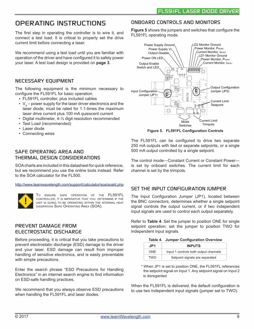
ONBOARD CONTROLS AND MONITORS
Figure 5 shows the jumpers and switches that configure the FL591FL operating mode.
ModeSwitches
Current LimitTrimpots
Output ConfigurationJumper (JP2)
Current LimitTestpoint
ENABLE
DISINPUT 1
INPUT 2
TRIMPOT
TRIMPOT
BNC
BNC
VSET 1
VSET 2GND
GNDLD1 MODECC CP CPCC
LD2 MODE LIM 1 LIM 2
LDA
LDA
PDA
PDA
LDC
LDC
LD 1
MON
1D
IS
VS GN
D
]ON
]OFF
]ONE
]TWO
]OFF
]ON
LD 2]S
]P
RPD1
RPD2
FL500POWER
Output Enable Switch and LED
Power ON LED
Input ConfigurationJumper (JP1)
Current Monitor, IMON1
Power Monitor, PMON1
LD1 Monitor GroundCurrent Monitor, IMON2
Power Monitor, PMON2
LD2 Monitor Ground
Output DisablePower Supply VS
Power Supply Ground
J4
Figure 5. FL591FL Configuration Controls
The FL591FL can be configured to drive two separate 250 mA outputs with tied or separate setpoints, or a single 500 mA output controlled by a single setpoint.
The control mode—Constant Current or Constant Power—is set by onboard switches. The current limit for each channel is set by the trimpots.
SET THE INPUT CONFIGURATION JUMPER
The Input Configuration Jumper (JP1), located between the BNC connectors, determines whether a single setpoint signal controls the output current, or if two independent input signals are used to control each output separately.
Refer to Table 4. Set the jumper to position ONE for single setpoint operation; set the jumper to position TWO for independent input signals.
Table 4. Jumper Configuration OverviewJP1 INPUTSONE Input 1 controls both output channels
TWO Setpoint signals are separated
* When JP1 is set to position ONE, the FL591FL references the setpoint signal on Input 1. Any setpoint signal on Input 2 is disregarded.
When the FL591FL is delivered, the default configuration is to use two independent input signals (jumper set to TWO).
© 2017 www.teamWavelength.com 9
FL591FL LASER DIODE DRIVER
SET THE OUTPUT CONFIGURATION JUMPER
The Output Configuration Jumper (JP2), located between the output connectors, determines whether the outputs are paralleled to drive up to 500 mA output on a single channel, or separate to drive up to 250 mA on two channels.
When the driver outputs are separate, connect each laser diode to the respective output connector, LD1 and LD2.
When the driver outputs are paralleled, each channel drives one-half of the total output current. When operating in parallel driver mode, use output connector LD1 to drive current to the load.
When the FL591FL is delivered, the default configuration is with two separate 250 mA output channels (jumper set to “S”).
WIRE THE POWER SUPPLY AND TEST LOAD
Wire the FL591FL power supply according to Figure 2, use the test load shown in Figure 4.
When the power supply is switched on, power is applied to the FL500 and the POWER LED will illuminate, but the output current is not enabled.
SET THE DRIVE CURRENT LIMITS; SEPARATE OUTPUT CONFIGURATION
First calculate the VLIM voltage; use the transfer function on page 5 according to your input/output configuration:
VLIM = ILIMx / Transfer Function (Separate) (V)
Connect the DMM to the LIM1 testpoint and the GND testpoint, and apply power to the FL591FL. Adjust the LIM1 trimpot until the voltage displayed on the DMM matches the VLIM value calculated above. Turn the trimpot clockwise to increase the current limit.
Connect the DMM to the LIM2 testpoint, and set the current limit on channel two using the same procedure.
SET THE DRIVE CURRENT LIMITS; PARALLEL OUTPUT CONFIGURATION
If the FL591FL is configured to drive paralleled outputs, the current limit is set using the LIM1 trimpot only.
First calculate the VLIM voltage; use the transfer function on page 5 based on your input/output configuration:
VLIM = ILIM1 / Transfer Function (Parallel) (V)
Connect the DMM to the LIM1 testpoint and the GND testpoint, and apply power to the FL591FL. Adjust the LIM1 trimpot until the voltage displayed on the DMM matches the VLIM value calculated above.
CONFIGURE FOR CONSTANT CURRENT OR CONSTANT POWER MODE
The FL591FL will drive lasers in Constant Current mode or Constant Power mode. Constant Power mode operation requires photodiode feedback from the laser.
To configure channel one for Constant Current mode operation, set the LD1 MODE switch to CC (left); for Constant Power mode set the switch to CP (right). Set channel two in the same manner.
!do not change swItch posItIons whIle power Is applIed to the fl591fl. doIng so may damage the laser. remove power from the fl591fl board before changIng mode swItch posItIons.
If the FL591FL outputs are paralleled and operated in CP-mode, the signal on the channel one photodiode is used in the control feedback loop.
When the FL591FL is delivered, the default configuration is Constant Current mode on both channels.
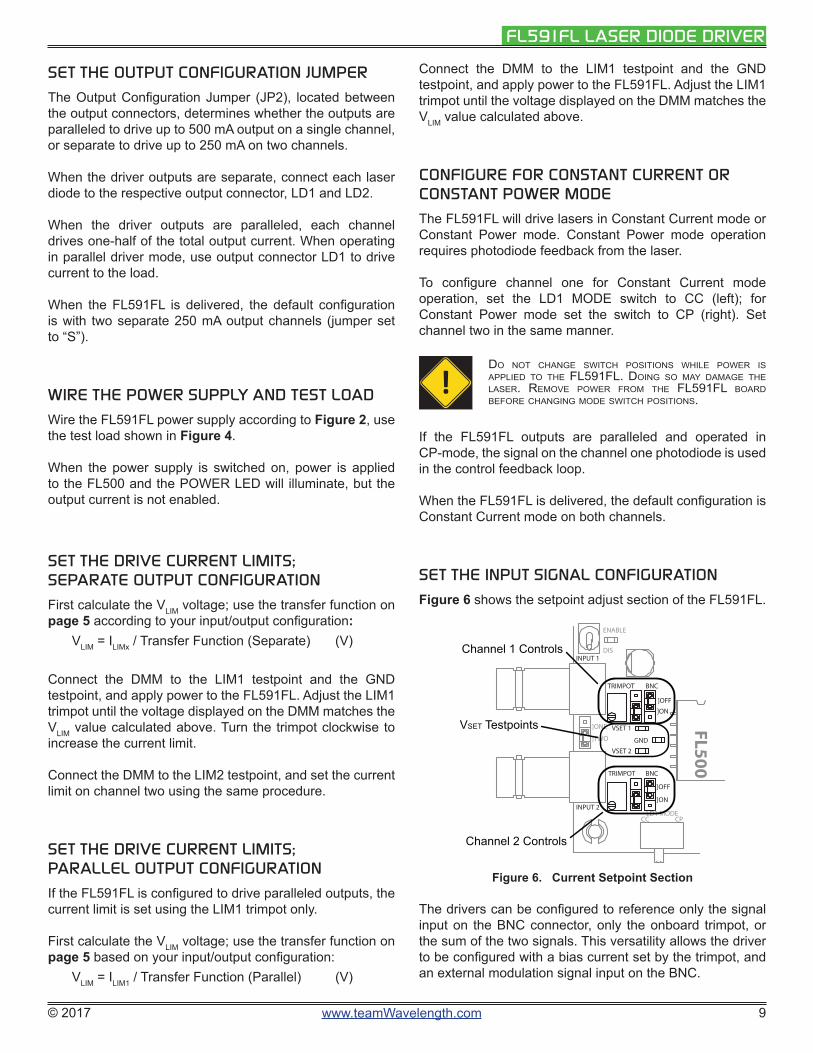
SET THE INPUT SIGNAL CONFIGURATION
Figure 6 shows the setpoint adjust section of the FL591FL.
ENABLE
DISINPUT 1
INPUT 2
TRIMPOT
TRIMPOT
BNC
BNC
VSET 1
VSET 2GND
LD1 MODECC CP
]ON
]OFF
]ONE
]TWO
]OFF
]ON
Channel 2 Controls
VSET Testpoints
Channel 1 Controls
LD1 MODECC CP
FL500
Figure 6. Current Setpoint Section
The drivers can be configured to reference only the signal input on the BNC connector, only the onboard trimpot, or the sum of the two signals. This versatility allows the driver to be configured with a bias current set by the trimpot, and an external modulation signal input on the BNC.
© 2017 www.teamWavelength.com 10
FL591FL LASER DIODE DRIVER
Configure the setpoint jumpers per Table 5. Channels one and two are configured independently.
Table 5. Setpoint Jumper ConfigurationTRIMPOT BNC EFFECT
OFFOFF This setting results in no setpoint input
signal; Do not use this setting
ON Reference only the BNC signal
ONOFF Reference only the onboard trimpot
ON Add the BNC signal to the onboard trimpot setpoint value
When the FL591FL is delivered it is configured to reference only the onboard trimpot setpoint signals.
CONNECT THE CURRENT AND POWER MONITORS
Connector J4, the screw terminal at the top of the board, includes outputs for monitoring the drive current and photodiode currents of both channels. Wire the DMM per Figure 2 on page 2 to monitor these signals. The transfer functions are listed in Table 2 on page 5.
ENABLE THE OUTPUT CURRENT
In order to enable the output current, two conditions must be met simultaneously:
• The DIS pin on the power connector must be grounded.• The output ENABLE switch must be set to ENABLE.
Channels one and two are enabled simultaneously, whether the FL591FL is in separate- or parallel-output mode. When the output is enabled, the LED next to the ENABLE switch will illuminate.
The output is disabled by floating the DIS pin or applying a 3 – 5 VDC signal, or by setting the ENABLE switch to DISABLE.
ADJUST THE OUTPUT CURRENT SETPOINT IN CONSTANT CURRENT MODE
Calculate the VSET voltage value using the equation below. Use the proper CC-mode transfer function for dual- or single-channel operation (see Table 2).
VSET = ILD / Transfer Function (V)
Connect the positive lead of the DMM to the VSET1 testpoint, and the negative lead to the GND testpoint and adjust the VSET1 trimpot until the voltage value on the DMM matches the value calculated above. Turning the trimpot clockwise increases the output current.
Repeat the process on the second channel if operating in dual-channel mode.
ADJUST THE OUTPUT CURRENT SETPOINT IN CONSTANT POWER MODE
In Constant Power mode, the drive current is not set directly. Rather, the photodiode current setpoint is calculated and set; the controller adjusts the output current in order to maintain the required photodiode current.
Refer to the laser diode datasheet to find the photodiode current at the desired optical output power level. Then calculate the VSET voltage value using the equation below, and the CP-mode transfer function listed in Table 2.
VSET = IPD / Transfer Function (V)
Connect the positive lead of the DMM to the VSET1 testpoint, and the negative lead to the GND testpoint and adjust the VSET1 trimpot until the voltage on the DMM matches the VSET voltage. Turning the trimpot clockwise increases the Constant Power setpoint current.
Repeat the process on the second channel if operating in dual-channel mode.
RECONFIGURE FOR YOUR APPLICATION
Once you are familiar with the operation of the FL591FL, switch off the output and power supplies, and remove the test load. Wire your laser diode according to the wire diagram shown in Figure 2 on page 2.
© 2017 www.teamWavelength.com 11
FL591FL LASER DIODE DRIVER
TROUBLESHOOTING
PROBLEM POTENTIAL CAUSES SOLUTIONSDriver will not switch on Improperly configured power
supplyCarefully check the wiring diagram on page 2. Make sure the power supply polarity is not reversed.
Power supply voltage too low Check the electrical specifications on page 6 and make sure the power supply is within the required voltage range to operate the FL591FL.
Output will not enable Improperly configured Enable switch on the FL591FL
The DIS pin on the Power connector must be grounded AND the switch on the FL591FL must be set to ENABLE.
Power supply voltage too low Check the electrical specifications on page 6 and make sure the power supply is within the required voltage range to operate the FL591FL.
Driver not working properly in constant current, parallel-output mode
Jumpers configured incorrectly Check page 9 to make sure the output jumper is set properly.
Improper output wiring configuration
Check that the connections to the laser diode are made via output connector LD1.
Laser output power too low in Constant Current mode
Laser current setpoint too low Increase the setpoint either by adjusting the trimpot, or by increasing the signal voltage on the input connector.
Laser current limit too low Refer to page 9 for instructions on setting the laser driver current limit.
Laser driver is compliance limited Check the laser diode specifications to determine the forward voltage (VF). Make sure that the FL591FL is not compliance limited. Refer to the Electrical Specifications table on page 6.
Laser does not reach desired output in Constant Power mode
Current limit too low Check the laser diode datasheet to determine the approximate laser drive current at the desired optical power output level. Then verify that the current limit is set slightly higher than that. Refer to page 9 for instructions on setting the laser driver current limit.
Photodiode feedback current is out of range for the FL591FL
Refer to page 12 for information on adjusting the photodiode current range.
© 2017 www.teamWavelength.com 12
FL591FL LASER DIODE DRIVER
ADJUST THE PHOTODIODE CURRENT RANGE
The maximum photodiode current input is 1 mA, but the range can be adjusted by changing a resistor on the FL591FL circuit board. The location of the resistors is shown in Figure 7. The default resistor value is 1 kΩ ±1%.
Figure 7. Photodiode Feedback Resistors
GNDLIM 1 LIM 2
LDA
LDA
PDA
PDA
LDC
LDC
LD 1
LD 2]S
]P
RPD1
RPD2
FL500
Channel 1 PD Resistor
Channel 2 PD Resistor
Calculate new resistor values based on the expected maximum photodiode current using this equation:
RPD = 1 / IPMON (Ω)
To convert the VPMON value to photodiode current, use this equation:
IPMON = VPMON / (2 * RPD) (A)
TECHNICAL SUPPORT INFORMATIONThis section includes useful technical information on these topics:
• Adjust the Photodiode Current Range• FL591FL Schematic• Safe Operating Area Calculation
© 2017 www.teamWavelength.com 13
FL591FL LASER DIODE DRIVER
PDFB
1
PDFB
2
PSET
1
PSET
2
S2
CC
/CP
1
S3
CC
/CP
2
D8
LM40
40-2
.5
5
4 3Q4A
2
16
Q4B
MM
DT3
946
R84 249
2
3 1
W
CW CCWR82 2.0K
C46 10uF
C47 10uF
R81 182
VCC
2 31
8 4
U4A
AD
8032
2 31
8 4
U6A
AD
8032
VCC
-U4
VCC
-U6
VEE
-U6
R78
1.05
K
Q1 BS
S138
VCC
R27 499
R28 499
VCC
R61 10.0
VCC
1
GN
D2
RST
3
VSE
T14
GN
D5
VSE
T26
LDC2
7LD
C28
PGN
D9
PGN
D10
LDC1
11LD
C112
U5 FL50
0
PDA
1
PDA
2
VS
LDA
2LD
A1
LDC
3PD
A2
LDA
1
J1 LD C
onn
LDC
3PD
A2
LDA
1
J2 LD C
onn
1 2 3JP
2
VS-
U7
IMO
N1
IMO
N2
VEE
-U7
R57 1.0
R48 1.0
2 31
8 4
U7A
AD
8032
567
U7B
AD
8032
C17 10uF
C16 10uF
C26 10uF
C48
10uF
D10
LM40
40-2
.5
5
4 3Q5A
2
16
Q5B
MM
DT3
946
R96 249
2
3 1
W
CW CCWR92 2.0K
C49 10uF
C50 10uF
R91 182
VCC
567
U4B
AD
8032
567
U6B
AD
8032
R90
1.05
K
C51
10uF
D7 1N
4148
D9 1N
4148
VSE
T2
VSE
T1
VS
EN1
GN
D3
VS
2
J4 Pow
er
21 3
S1 SPD
T To
ggle
C19 100u
FC
18 100u
F1 2 3
JP1
LDC2
IMO
N1
IMO
N2
PMO
N2
PMO
N1
MO
NIT
ORS
123456J3
TP
7Te
st Po
int
D2
SML-
LXT0
805G
W
D1
TP
6 (V
IA)
Test
Poin
t
TP
5 (V
IA)
Test
Poin
t
R20 1.0
R21 1.0
R77 1.0K
R76 1.0K
R85 1.0K
R75 1.0K R
831.
0K
R89 1.0K
R88 1.0K
R87 1.0K
R97 1.0K
R93 1.0K
R60
20.0
k
R56
20.0
k
R54
20.0
k
R45
20.0
k
R49 1.0K
R58
1.0K
R98 2.0K
R86
2.0K
R53
4.99
K
R44
4.99
K
R59
4.99
K
R55
4.99
K
TP
2LI
M1
TP
4LI
M2
LDA
1
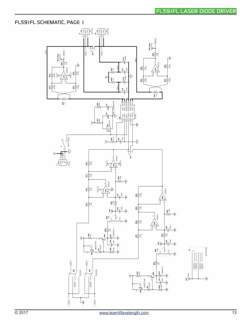
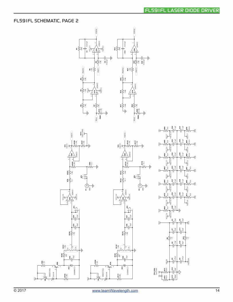
FL591FL SCHEMATIC, PAGE 1
© 2017 www.teamWavelength.com 14
FL591FL LASER DIODE DRIVER
2
3 1
W
CW CCWR10
12.
0K
C53 10uF
1 2 3
JP3
123
JP4
R80 51.1
R79 51.1
2 31
8 4
U8A
AD
8032
5 67
U8B
AD
8032
VEE
-U8
VCC
-U8
5
4 3Q6A
2
16
Q6B
MM
DT3
946
R99 182
C52 10uF
D12
LM40
40-2
.5
2
3 1
W
CW CCWR11
02.
0K
C56 10uF
1 2 3
JP5
123
JP6
R11
851
.1
R11
2
51.1
2 31
8 4
U9A
AD
8032
5 67
U9B
AD
8032
VEE
-U9
VCC
-U9
5
4 3Q7A
2
16
Q7B
MM
DT3
946
R10
818
2
C55 10uF
D14
LM40
40-2
.5
VEE
-U1
VEE
-U3
PDA
1
VS-
U1
VCC
-U3
PMO
N1
PSET
1P
DR
1
C1
0.01
2uF
C4
0.02
2uF
2 31
8 4
U1A
AD
8032
2 31
8 4
U3A
AD
8032
PDFB
1
PDA
2
PMO
N2
PSET
2PD
FB2
PD
R2
C14
0.01
2uF
C20
0.02
2uF
567
U1B
AD
8032
567
U3B
AD
8032
D11
1N41
48
D13
1N41
48
VSE
T1
VSE
T2
P2 BN
C
P1 BN
C
VEE
VS
VEE
RAW
R8 1.0
R16 1.0
R12 10.0
R13 10.0
C12
10uF
C5
0.47
uF
C9
0.47
uF
C6
4.7u
F
C10
10uF
VS
VEE
Filte
r for
U1
VS-
U1
VEE
-U1
VCC VEE
Filte
r for
U3
VCC
-U3
VEE
-U3
VCC VEE
Filte
r for
U6
VCC
-U6
VEE
-U6
VS
VEE
Filte
r for
U7
VS-
U7
VEE
-U7
C21
0.1u
F
C28
0.1u
F
C22
0.1u
F
C29
0.1u
F
C23
0.1u
F
C30
0.1u
F
C24
0.1u
F
C31
0.1u
F
R63
10.0
R67 10.0
R64
10.0
R68 10
.0
R65
10.0
R69 10
.0
R66
10.0
R70 10
.0
VCC VEE
Filte
r for
U8
VCC
-U8
VEE
-U8
C35
0.1u
F
C36
0.1u
F
R72
10.0
R73 10.0
VCC VEE
Filte
r for
U9
VC
C-U
9
VEE
-U9
C37
0.1u
F
C38
0.1u
F
R94
10.0
R95 10.0
VRA
W
VCC
Filte
r for
U4
VCC
-U4
C25
0.1u
F
R62
10.0
VCC
C13
100u
F
VCC
VCC
C57 22uF
C54 22uF
C3
22uF C8
22uF
R10
3
1.0K
R10
51.
0K
R10
4
1.0K
R11
4
1.0K
R11
3
1.0K
R11
51.
0K
R10
61.
0K
R10
71.
0K
R11
61.
0K
R11
71.
0K
R2
1.0K
R3
1.0K
R4
1.0K
R7
1.0K R17
1.0K
R18 1.0K
R19
1.0K
R24
1.0K
R23
1.0K
R25
1.0K
R6
1.0K
R9
1.0K
R1
100k
R14
100k
R10
22.
0K
R11
12.
0K
R10
9
499
R10
0
499
TP
3V
SET2
TP
1V
SET1
TP
11V
SET
GN
D
C11
22uFC7
22uF
R10 1.0K
R26 1.0K
TP
4 (V
IA)
Test
Poin
t
FL591FL SCHEMATIC, PAGE 2
© 2017 www.teamWavelength.com 15
FL591FL LASER DIODE DRIVER
1.0 2.0 3.0 4.0 5.0 6.0 7.0 8.0 9.00.00
0.05
0.10
0.15
0.20
0.25
Voltage (V)
Cur
rent
(A)
VDROP VS
IMAX
Load Line
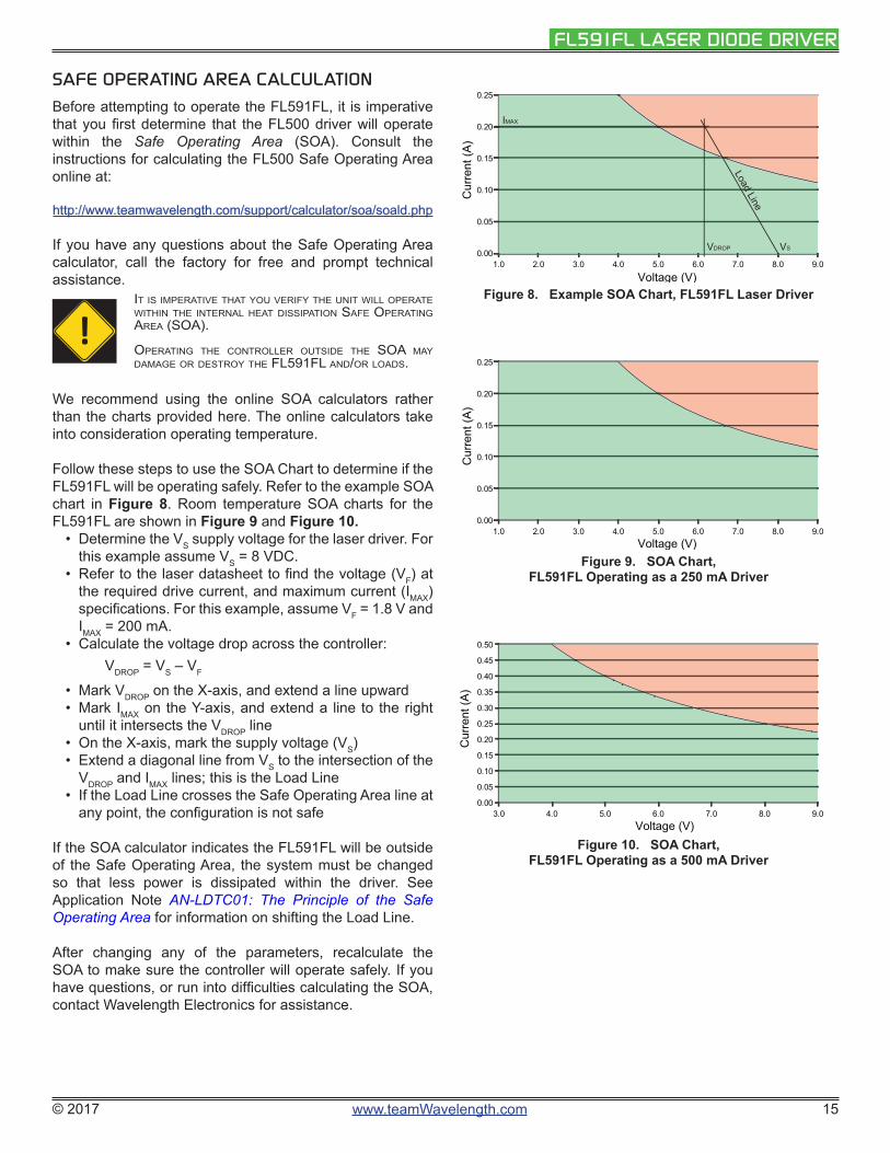
Figure 8. Example SOA Chart, FL591FL Laser Driver
1.0 2.0 3.0 4.0 5.0 6.0 7.0 8.0 9.00.00
0.05
0.10
0.15
0.20
0.25
Voltage (V)
Cur
rent
(A)
Figure 9. SOA Chart, FL591FL Operating as a 250 mA Driver
3.0 4.0 5.0 6.0 7.0 8.0 9.00.00
0.05
0.10
0.15
0.20
0.25
0.30
0.35
0.40
0.45
0.50
Voltage (V)
Cur
rent
(A)
Figure 10. SOA Chart, FL591FL Operating as a 500 mA Driver
SAFE OPERATING AREA CALCULATION
Before attempting to operate the FL591FL, it is imperative that you first determine that the FL500 driver will operate within the Safe Operating Area (SOA). Consult the instructions for calculating the FL500 Safe Operating Area online at:
http://www.teamwavelength.com/support/calculator/soa/soald.php
If you have any questions about the Safe Operating Area calculator, call the factory for free and prompt technical assistance.
!It Is ImperatIve that you verIfy the unIt wIll operate wIthIn the Internal heat dIssIpatIon safe operatIng area (soa).
operatIng the controller outsIde the soa may damage or destroy the fl591fl and/or loads.
We recommend using the online SOA calculators rather than the charts provided here. The online calculators take into consideration operating temperature.
Follow these steps to use the SOA Chart to determine if the FL591FL will be operating safely. Refer to the example SOA chart in Figure 8. Room temperature SOA charts for the FL591FL are shown in Figure 9 and Figure 10.
• Determine the VS supply voltage for the laser driver. For this example assume VS = 8 VDC.
• Refer to the laser datasheet to find the voltage (VF) at the required drive current, and maximum current (IMAX) specifications. For this example, assume VF = 1.8 V and IMAX = 200 mA.
• Calculate the voltage drop across the controller: VDROP = VS – VF
• Mark VDROP on the X-axis, and extend a line upward• Mark IMAX on the Y-axis, and extend a line to the right
until it intersects the VDROP line• On the X-axis, mark the supply voltage (VS) • Extend a diagonal line from VS to the intersection of the
VDROP and IMAX lines; this is the Load Line• If the Load Line crosses the Safe Operating Area line at
any point, the configuration is not safe
If the SOA calculator indicates the FL591FL will be outside of the Safe Operating Area, the system must be changed so that less power is dissipated within the driver. See Application Note AN-LDTC01: The Principle of the Safe Operating Area for information on shifting the Load Line.
After changing any of the parameters, recalculate the SOA to make sure the controller will operate safely. If you have questions, or run into difficulties calculating the SOA, contact Wavelength Electronics for assistance.
© 2017 www.teamWavelength.com 16
FL591FL LASER DIODE DRIVER
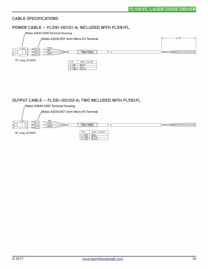
CABLE SPECIFICATIONS
POWER CABLE -- FL591-00101-A; INCLUDED WITH FL591FL
1
32
Molex 43645-0300 Terminal Housing
Molex 43030-007 3mm Micro-Fit Terminal
1 - DIS2 - VS3 - GND
18” Long, 22 AWG
OUTPUT CABLE -- FL591-00102-A; TWO INCLUDED WITH FL591FL
1
32
1 - LDA2 - PDA3 - LDC
Molex 43645-0300 Terminal Housing
Molex 43030-007 3mm Micro-Fit Terminal
18” Long, 22 AWG
© 2017 www.teamWavelength.com 17
FL591FL LASER DIODE DRIVER
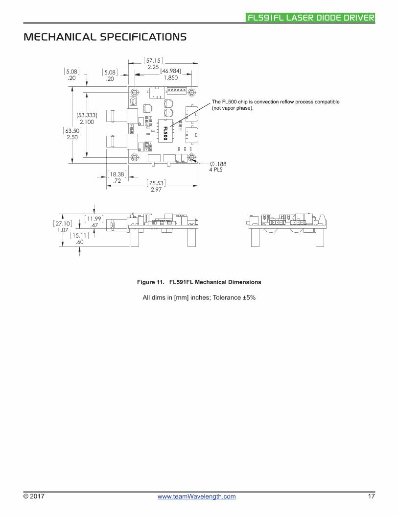
MECHANICAL SPECIFICATIONS
11.99.47
15.11.60
27.101.07
[46.984]1.850
5.08.20
57.152.25
[53.333]2.100
5.08.20
63.502.50
18.38.72
75.532.97
.1884 PLS
The FL500 chip is convection reflow process compatible(not vapor phase).
FL500
Figure 11. FL591FL Mechanical Dimensions
All dims in [mm] inches; Tolerance ±5%
© 2017 www.teamWavelength.com 18
FL591FL LASER DIODE DRIVER
CERTIFICATION AND WARRANTY
CERTIFICATION
Wavelength Electronics, Inc. (Wavelength) certifies that this product met its published specifications at the time of shipment. Wavelength further certifies that its calibration measurements are traceable to the United States National Institute of Standards and Technology, to the extent allowed by that organization’s calibration facilities, and to the calibration facilities of other International Standards Organization members.
WARRANTY
This Wavelength product is warranted against defects in materials and workmanship for a period of one (1) year from date of shipment. During the warranty period, Wavelength will, at its option, either repair or replace products which prove to be defective.
WARRANTY SERVICE
For warranty service or repair, this product must be returned to the factory. An RMA is required for products returned to Wavelength for warranty service. The Buyer shall prepay shipping charges to Wavelength and Wavelength shall pay shipping charges to return the product to the Buyer upon determination of defective materials or workmanship. However, the Buyer shall pay all shipping charges, duties, and taxes for products returned to Wavelength from another country.
LIMITATIONS OF WARRANTY
The warranty shall not apply to defects resulting from improper use or misuse of the product or operation outside published specifications. No other warranty is expressed or implied. Wavelength specifically disclaims the implied warranties of merchantability and fitness for a particular purpose.
EXCLUSIVE REMEDIES
The remedies provided herein are the Buyer’s sole and exclusive remedies. Wavelength shall not be liable for any direct, indirect, special, incidental, or consequential damages, whether based on contract, tort, or any other legal theory.
REVERSE ENGINEERING PROHIBITED
Buyer, End-User, or Third-Party Reseller are expressly prohibited from reverse engineering, decompiling, or disassembling this product.
NOTICE
The information contained in this document is subject to change without notice. Wavelength will not be liable for errors contained herein or for incidental or consequential damages in connection with the furnishing, performance, or use of this material. No part of this document may be translated to another language without the prior written consent of Wavelength.
SAFETY
There are no user-serviceable parts inside this product. Return the product to Wavelength Electronics for service and repair to ensure that safety features are maintained.
LIFE SUPPORT POLICY
This important safety information applies to all Wavelength electrical and electronic products and accessories:
As a general policy, Wavelength Electronics, Inc. does not recommend the use of any of its products in life support applications where the failure or malfunction of the Wavelength product can be reasonably expected to cause failure of the life support device or to significantly affect its safety or effectiveness. Wavelength will not knowingly sell its products for use in such applications unless it receives written assurances satisfactory to Wavelength that the risks of injury or damage have been minimized, the customer assumes all such risks, and there is no product liability for Wavelength. Examples of devices considered to be life support devices are neonatal oxygen analyzers, nerve stimulators (for any use), auto-transfusion devices, blood pumps, defibrillators, arrhythmia detectors and alarms, pacemakers, hemodialysis systems, peritoneal dialysis systems, ventilators of all types, and infusion pumps as well as other devices designated as “critical” by the FDA. The above are representative examples only and are not intended to be conclusive or exclusive of any other life support device.
REVISION HISTORYDOCUMENT NUMBER: FL591-00400
REV. DATE CHANGEF Nov 2012 Update datasheet for FL591FL
product enhancementG March 2014 Clarified reflow compatibilityH June 2014 Updated Transfer FunctionsI February 2017 Updated max supply voltage value
51 Evergreen DriveBozeman, Montana 59771
406-587-4910 (tel)406-587-4911 (fax)
Sales & Tech [email protected]