D-Σ Digital Control. Wu.pdf · Elegant Power Electronics Applied Research Laboratory (EPEARL) 10...
72
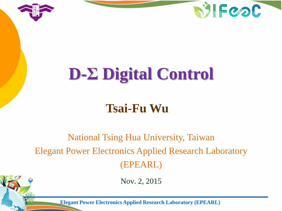
Elegant Power Electronics Applied Research Laboratory (EPEARL) D-Σ Digital Control Nov. 2, 2015 Tsai-Fu Wu National Tsing Hua University, Taiwan Elegant Power Electronics Applied Research Laboratory (EPEARL)
Transcript of D-Σ Digital Control. Wu.pdf · Elegant Power Electronics Applied Research Laboratory (EPEARL) 10...
Elegant Power Electronics Applied Research Laboratory (EPEARL)
D-Σ Digital Control
Nov. 2, 2015
Tsai-Fu Wu
National Tsing Hua University, Taiwan
Elegant Power Electronics Applied Research Laboratory
(EPEARL)
Elegant Power Electronics Applied Research Laboratory (EPEARL) 2
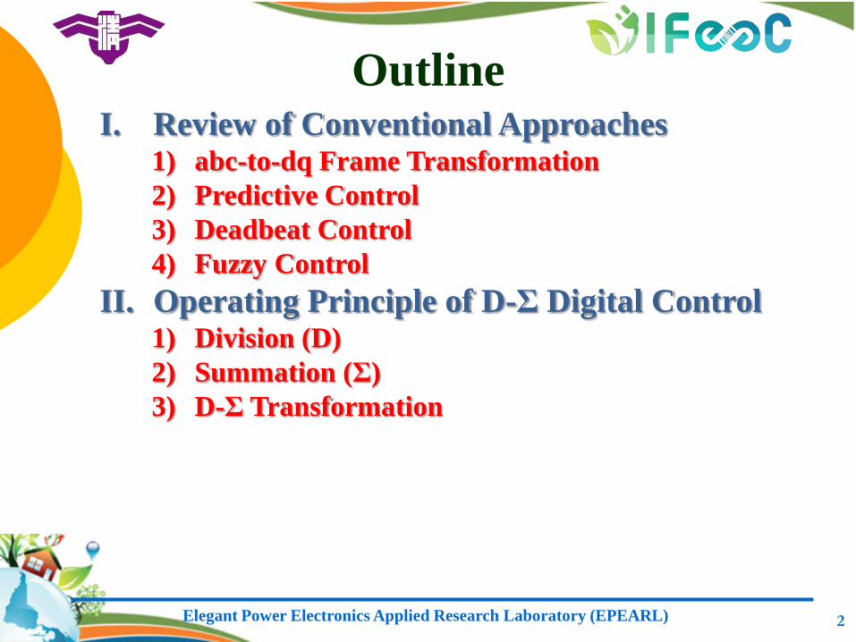
Outline I. Review of Conventional Approaches
1) abc-to-dq Frame Transformation
2) Predictive Control
3) Deadbeat Control
4) Fuzzy Control
II. Operating Principle of D-Σ Digital Control 1) Division (D)
2) Summation (Σ)
3) D-Σ Transformation
Elegant Power Electronics Applied Research Laboratory (EPEARL) 3
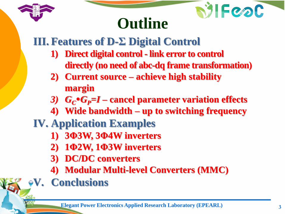
Outline III. Features of D-Σ Digital Control
1) Direct digital control - link error to control
directly (no need of abc-dq frame transformation)
2) Current source – achieve high stability
margin
3) GCGP=I – cancel parameter variation effects
4) Wide bandwidth – up to switching frequency
IV. Application Examples 1) 3Φ3W, 3Φ4W inverters
2) 1Φ2W, 1Φ3W inverters
3) DC/DC converters
4) Modular Multi-level Converters (MMC)
V. Conclusions
Elegant Power Electronics Applied Research Laboratory (EPEARL) 4
I. Review of Conventional Approaches 1) abc-to-dq frame transformation
c
b
a
q
d
x
x
x
x
x
3
2sin
3
2sinsin
3
2cos
3
2coscos
•State Equations
TN
SN
RN
TN
SN
RN
T
S
R
v
v
v
Lu
u
u
Li
i
i
dt
d 11
oq
od
q
d
q
d
q
d
v
v
L
L
u
u
L
L
i
i
i
i
dt
d
/10
0/1
/10
0/1
0
0
LLLL TSR
A. Converter Configuration
Elegant Power Electronics Applied Research Laboratory (EPEARL) 5
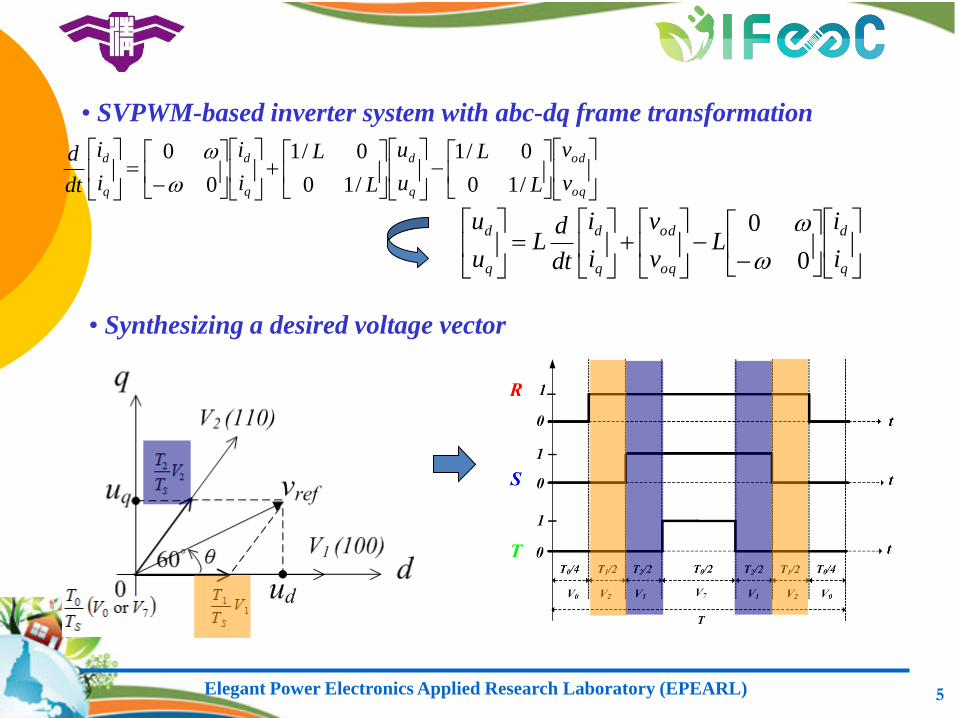
• SVPWM-based inverter system with abc-dq frame transformation
• Synthesizing a desired voltage vector
q
d
oq
od
q
d
q
d
i
iL
v
v
i
i
dt
dL
u
u
0
0
oq
od
q
d
q
d
q
d
v
v
L
L
u
u
L
L
i
i
i
i
dt
d
/10
0/1
/10
0/1
0
0
Elegant Power Electronics Applied Research Laboratory (EPEARL) 6
id*
Σ
Σiq*
Voltage Vector Controller
id,e
iq,edq → abc
vd
vqSVPWM
3-PhaseInverter
θ
PWM
VDC
d,q ← a,b,cid
iq
iaib
ic
d,q ← a,b,cvgd
vgq
vaNvbN
vcN
L Lg Girda
b
c
Grid Angle θ
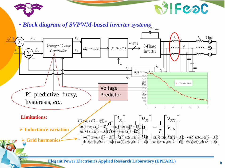
• Block diagram of SVPWM-based inverter systems
PI, predictive, fuzzy,
hysteresis, etc.
Inductance variation
Grid harmonics
Limitations:
Voltage Predictor
TN
SN
RN
T
S
R
S
S
R
v
v
v
Lu
u
u
Li
i
i
dt
d 11
0
500
1000
1500
2000
2500
3000
3500
4000
4500
5000
1 6 11 16 21 26 31 36
Inductance L(uH)
Elegant Power Electronics Applied Research Laboratory (EPEARL) 7
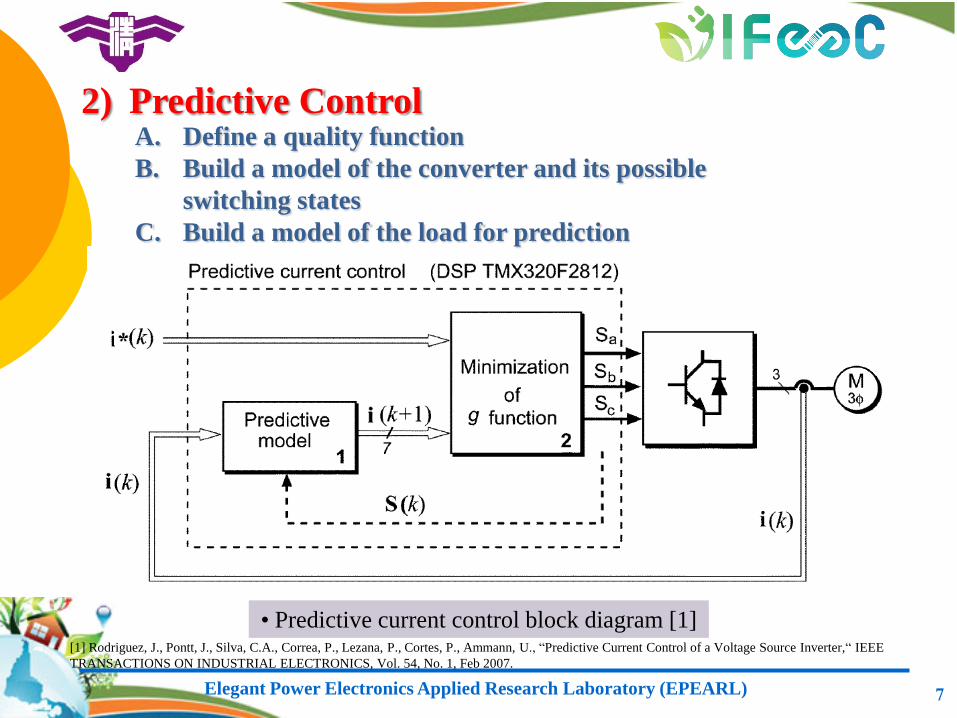
2) Predictive Control A. Define a quality function
B. Build a model of the converter and its possible
switching states
C. Build a model of the load for prediction
• Predictive current control block diagram [1] [1] Rodriguez, J., Pontt, J., Silva, C.A., Correa, P., Lezana, P., Cortes, P., Ammann, U., “Predictive Current Control of a Voltage Source Inverter,“ IEEE
TRANSACTIONS ON INDUSTRIAL ELECTRONICS, Vol. 54, No. 1, Feb 2007.
Elegant Power Electronics Applied Research Laboratory (EPEARL) 8
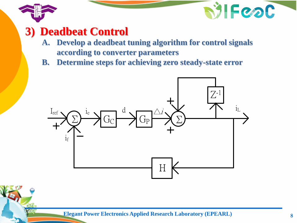
3) Deadbeat Control A. Develop a deadbeat tuning algorithm for control signals
according to converter parameters
B. Determine steps for achieving zero steady-state error
Iref
if
GC
d iL
H
△iΣ GP Σ
Z-1
ie
Elegant Power Electronics Applied Research Laboratory (EPEARL) 9
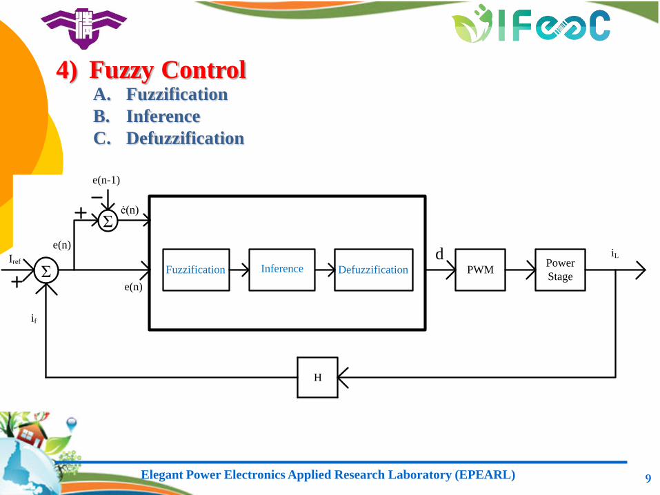
4) Fuzzy Control A. Fuzzification
B. Inference
C. Defuzzification
Iref
if
Fuzzification
dPWM
Power
Stage
iL
H
e(n)
e(n)
e(n-1)
ė(n)
Inference Defuzzification
Σ
Σ
Elegant Power Electronics Applied Research Laboratory (EPEARL) 10
II. Operational Principles of D-Σ Digital Control
1) No need of abc-dq frame transformation, the D-Σ digital
control determining control laws directly.
2) Unlike predictive control, the D-Σ digital control using all of the
information known a priori and no need of quality function.
3) Similar to deadbeat control, the D-Σ digital control determining
control law directly without frame transformation.
4) Unlike deadbeat control, the D-Σ digital control having a
controller to cover wide filter inductance, dc-bus voltage and
switching frequency variations.
5) Like fuzzy control, the D-Σ digital control being named based
on the processes of control-law derivation.
• Relationships to Conventional Approaches
Elegant Power Electronics Applied Research Laboratory (EPEARL) 11
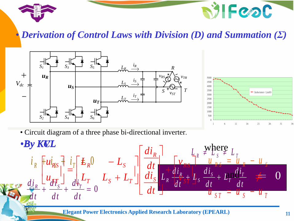
• Circuit diagram of a three phase bi-directional inverter.
0 TSR iii
0d t
d i
d t
d i
d t
d i TSR
S1
S2
S3 S5
S4 S6
R
S T
vRS
vST
vTR
LR
LS
LT
Vdc
uR
uS
uT
iR
iS
iT
d t
d iL
d t
d iL
d t
d iL T
TS
SR
R 0 ≠ =
•By KCL TSR LLL
ST
RS
S
R
TST
SR
ST
RS
v
v
dt
didt
di
LLL
LL
u
u SRR S uuu
TSS T uuu
where
and
•By KVL
0
500
1000
1500
2000
2500
3000
3500
4000
4500
5000
1 6 11 16 21 26 31 36
Inductance L(uH)
• Derivation of Control Laws with Division (D) and Summation (Σ)
Elegant Power Electronics Applied Research Laboratory (EPEARL) 12
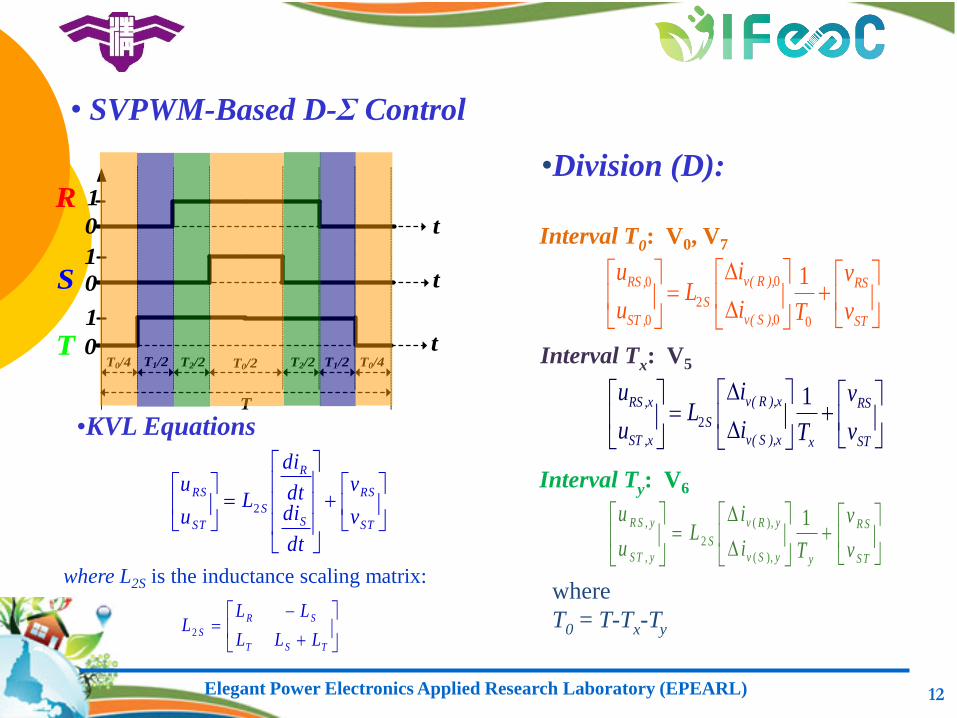
R
S
TT0/2
t
t
t
1
0
1
0
1
0
T
T2/2T1/2T0/4 T2/2 T1/2 T0/4
00
2
00 0
1v( R ),RS , RS
S
v( S ),ST , ST
iu vL
iu vT
S T
R S
yySv
yRv
S
yS T
yR S
v
v
Ti
iL
u
u 1
),(
),(
2
,
,
Interval T0: V0, V7
Interval Tx: V5
Interval Ty: V6
where
T0 = T-Tx-Ty
ST
RS
S
R
S
ST
RS
v
v
dt
didt
di
Lu
u2
•KVL Equations
• SVPWM-Based D-Σ Control
•Division (D):
TST
SR
SLLL
LLL2
where L2S is the inductance scaling matrix:
2
1v( R ),xRS ,x RS
S
v( S ),xST ,x STx
iu vL
iu vT
Elegant Power Electronics Applied Research Laboratory (EPEARL) 13
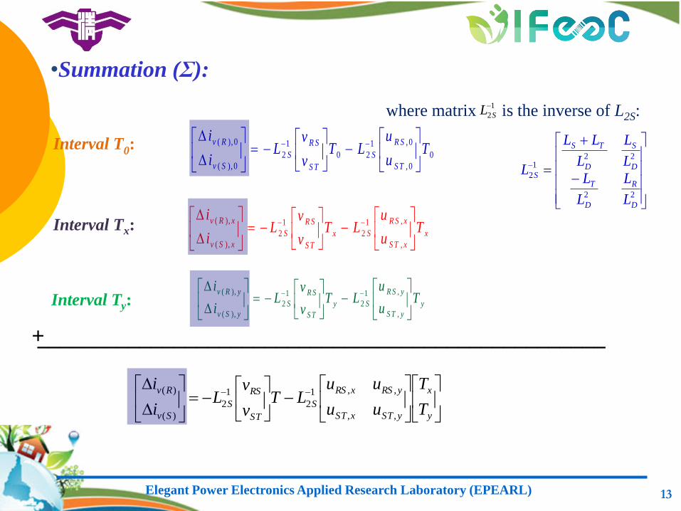
•Summation (Σ):
0
0,
0,1
20
1
2
0),(
0),(T
u
uLT
v
vL
i
i
S T
R S
S
S T
R S
S
Sv
Rv
x
xS T
xR S
Sx
S T
R S
S
xSv
xRvT
u
uLT
v
vL
i
i
,
,1
2
1
2
),(
),(
y
yS T
yR S
Sy
S T
R S
S
ySv
yRvT
u
uLT
v
vL
i
i
,
,1
2
1
2
),(
),(
Interval T0:
Interval Tx:
Interval Ty:
y
x
ySTxST
yRSxRS
S
ST
RS
S
Sv
Rv
T
T
uu
uuLT
v
vL
i
i
,,
,,1
2
1
2
)(
)(
+ __________________________________________________
22
221
2
D
R
D
T
D
S
D
TS
S
L
L
L
L
L
L
L
LL
L
where matrix is the inverse of L2S: 1
2
SL
Elegant Power Electronics Applied Research Laboratory (EPEARL) 14
Σ
Σ
i*w
i*x
iwf
ixf
-
-
+
+
Σ
Σ Σ Σ
Σ Σ GP(ww)
Hw
GP(xw)
Hx
e-sT
S
Δiw, e
Δix, e
iLw
iLx
e-sT
S
GP(wx)
GP(xx)
+
++
+++
+ ++
+
GC(ww)
GC(wx)
GC(xw)
GC(xx)
+
+
dw^
dx^
Δiw^
Δix^
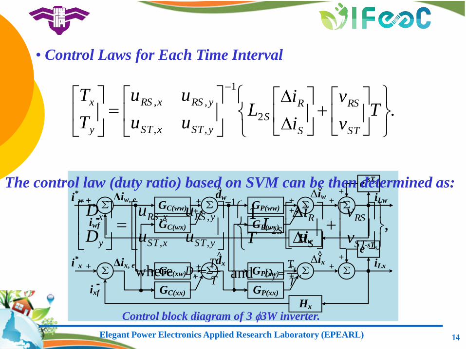
• Control Laws for Each Time Interval
.2
1
,,
,,
Tv
v
i
iL
uu
uu
T
T
ST
RS
S
R
S
ySTxST
yRSxRS
y
x
The control law (duty ratio) based on SVM can be then determined as:
,1
2
1
,,
,,
ST
RS
S
R
S
ySTxST
yRSxRS
y
x
v
v
i
iL
Tuu
uu
D
D
T
TD x
x .T
TD
y
y where and
Control block diagram of 3 3W inverter.
Elegant Power Electronics Applied Research Laboratory (EPEARL) 15
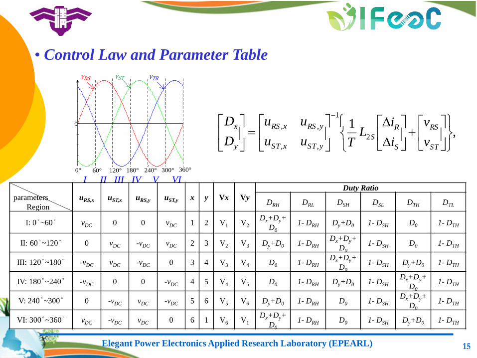
• Control Law and Parameter Table
,1
2
1
,,
,,
ST
RS
S
R
S
ySTxST
yRSxRS
y
x
v
v
i
iL
Tuu
uu
D
D0
I II III IV V VI60°0° 120° 180° 300°240° 360°
vTRvRS vST
parameters
Region
uRS,x uST,x uRS,y uST,y x y Vx Vy
Duty Ratio
DRH DRL DSH DSL DTH DTL
I: 0°~60° vDC 0 0 vDC 1 2 V1 V2 Dx+Dy+
D0 1- DRH Dy+D0 1- DSH D0 1- DTH
II: 60°~120° 0 vDC -vDC vDC 2 3 V2 V3 Dy+D0 1- DRH Dx+Dy+
D0 1- DSH D0 1- DTH
III: 120°~180° -vDC vDC -vDC 0 3 4 V3 V4 D0 1- DRH Dx+Dy+
D0 1- DSH Dy+D0 1- DTH
IV: 180°~240° -vDC 0 0 -vDC 4 5 V4 V5 D0 1- DRH Dy+D0 1- DSH Dx+Dy+
D0 1- DTH
V: 240°~300° 0 -vDC vDC -vDC 5 6 V5 V6 Dy+D0 1- DRH D0 1- DSH Dx+Dy+
D0 1- DTH
VI: 300°~360° vDC -vDC vDC 0 6 1 V6 V1 Dx+Dy+
D0 1- DRH D0 1- DSH Dy+D0 1- DTH
Elegant Power Electronics Applied Research Laboratory (EPEARL) 16
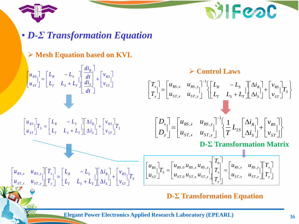
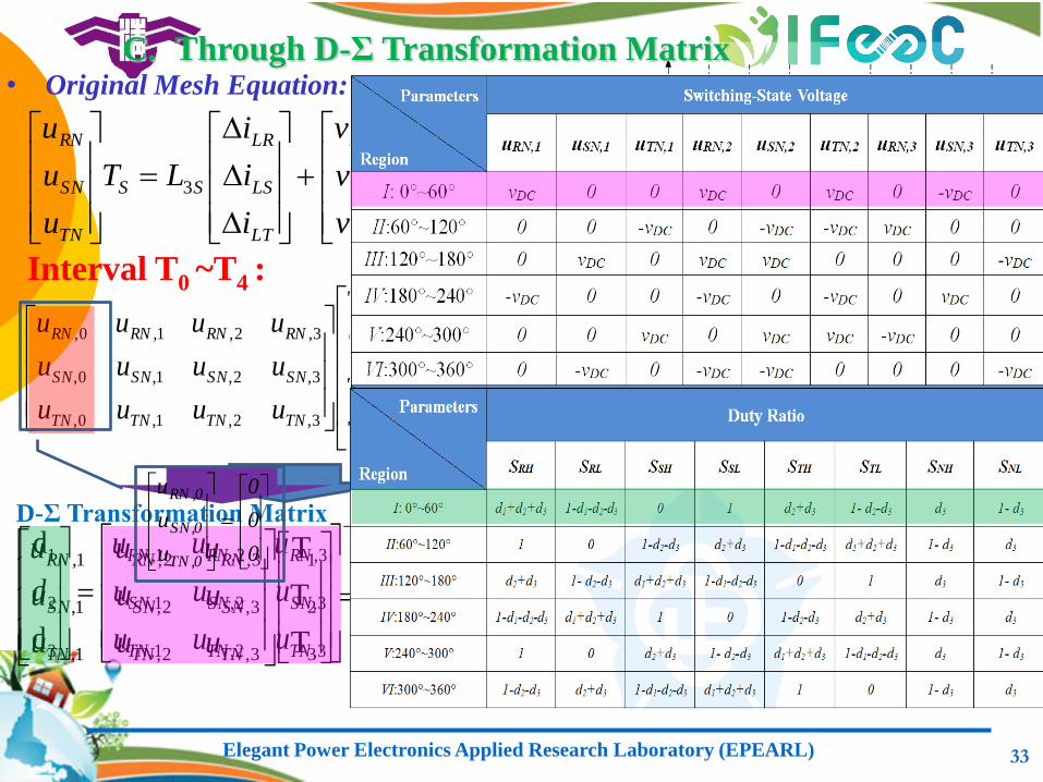
• D-Σ Transformation Equation
Mesh Equation based on KVL
ST
RS
S
R
TST
SR
ST
RS
v
v
dt
didt
di
LLL
LL
u
u
S
S T
R S
S
R
TST
SR
S
S T
R ST
v
v
i
i
LLL
LLT
u
u
S
ST
RS
S
R
TST
SR
y
x
ySTxST
yRSxRST
v
v
i
i
LLL
LL
T
T
uu
uu
,,
,,
Control Laws
S
ST
RS
S
R
TST
SR
ySTxST
yRSxRS
y
xT
v
v
i
i
LLL
LL
uu
uu
T
T1
,,
,,
y
x
ySTxST
yRSxRS
y
x
yST
yRS
xST
xRS
ST
RS
S
ST
RS
T
T
uu
uu
T
T
T
u
u
u
u
u
uT
u
u
,,
,,
0
,
,
,
,
0,
0,
ST
RS
S
R
S
ySTxST
yRSxRS
y
x
v
v
i
iL
Tuu
uu
D
D2
1
,,
,, 1
D-Σ Transformation Equation
D-Σ Transformation Matrix
Elegant Power Electronics Applied Research Laboratory (EPEARL) 17
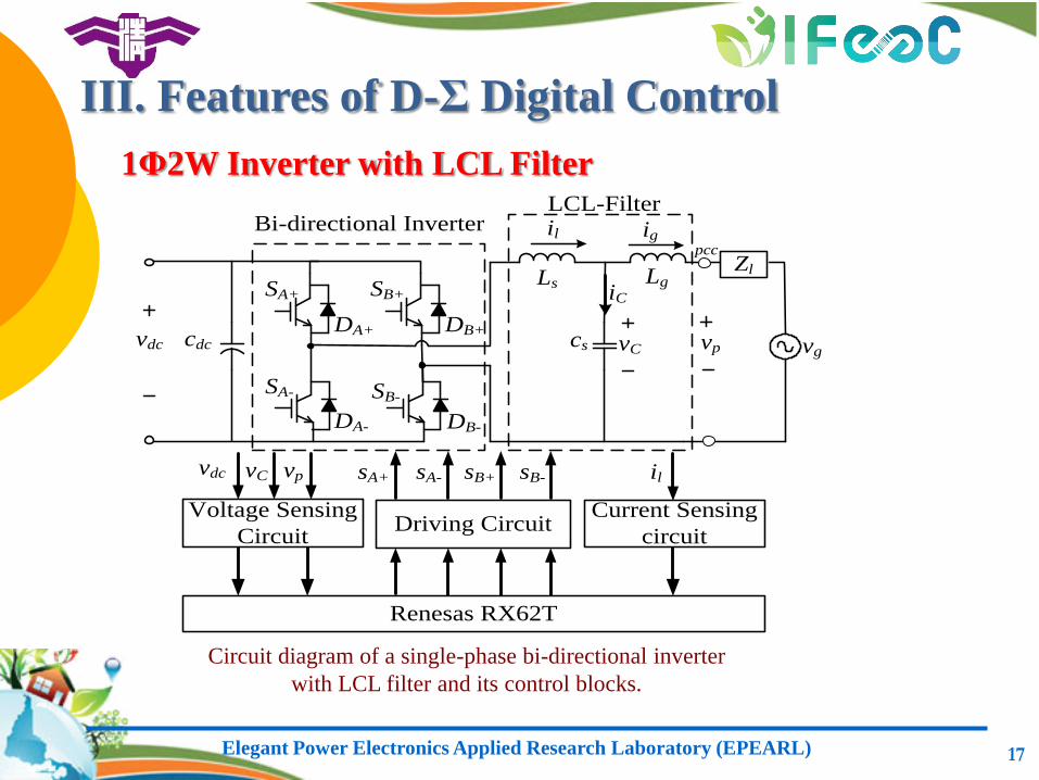
1Φ2W Inverter with LCL Filter
Circuit diagram of a single-phase bi-directional inverter
with LCL filter and its control blocks.
Ls
il
SA+ SB+
SA- SB-
DA+
DA-
DB+
DB-
vdc cdc cs vg
vdc vp
Driving Circuit
Renesas RX62T
Voltage Sensing
Circuit
Current Sensing
circuit
sA+ sA- sB+ sB- il
Lg
vC
iC
Bi-directional InverterLCL-Filter
ig
vC
Zl
vp
pcc
III. Features of D-Σ Digital Control
Elegant Power Electronics Applied Research Laboratory (EPEARL) 18
T1
Z/1GH
v
iG cilc
0Ip
g
iv
gr
-140
-120
-100
-80
-60
-40
-20
0
20
Magn
itu
de (
dB
)
-45
0
45
90
Ph
ase
(d
eg)
101 102 103 104 105
Frequency (Hz)
-40-20
0
20
40
60
80
100
120
140
Ma
gn
itu
de (
dB
)
101
102 103 104 10545
90
135
180
225
Ph
ase
(d
eg
)
Frequency (Hz)
-40
-20
0
20
40
60
80
100
120
140
Ma
gn
itu
de (
dB
)
-90
-45
0
45
90
Ph
ase
(d
eg)
101 102 103 104 105
Frequency (Hz)
Zo1: Ls = 1.5 mH, Lg = 500µH
Zo2: Ls = 1.5 mH, Lg = 420µH
Zo3: Ls = 600 µH, Lg = 500µH
Zo4: Ls = 600 µH, Lg = 420µH
Zl
++
-
++
+-
++
Σ Σ ΣGc Gp
H1
i*lrIgr ile
ilf
d
1/Zc
il
vc Σ
Σ ig
vp
Δil
vc-vp
+
e-sTs
icZg
D- ControlΣ
ic~
Cs /Ts
-e-sTs
Σ+
s
s
sdcl
L
Tv2
d
i
d
ilGp
sdc
s
p Tv2
L
G
1Gc
ssT
1pc
pc
ileHGG1
GGG
T1
G
I
iG il
0vgr
g
ig
p
++Σ
i*lrIgr il
Hc
vp
ig
Zg
Σ
Σ
ic
+-
+
+
Gil
1/ZC
ic~
equivalent transformation
Note: e-sT is approximated as (1-sTs)
vg
Zl
vpZo
ip
ig
is
T
)T1(ZZ
g
o
ilgc
c
gGZH
Z
ZT
s
sT
sc
T
)e1(CH
s
control block diagram of the proposed filter-capacitor
current compensation and based on D-Σ digital control
Equivalent circuit of the controlled current-source
inverter connected to the grid with grid impedance Zl.
0P
g
VZ
i
• s-domain model
Elegant Power Electronics Applied Research Laboratory (EPEARL) 19
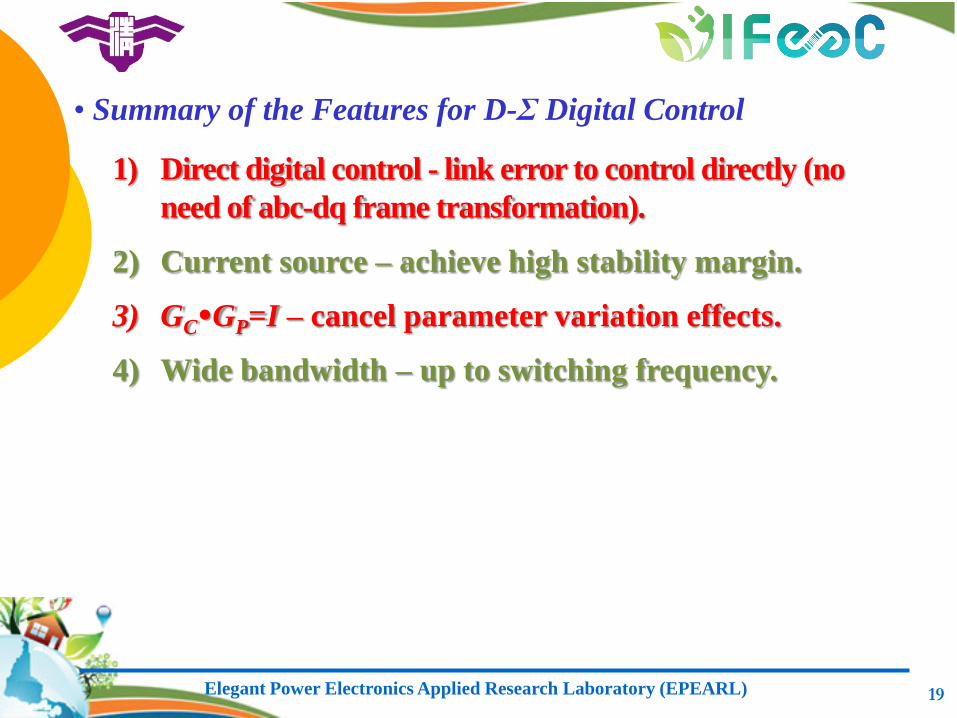
1) Direct digital control - link error to control directly (no
need of abc-dq frame transformation).
2) Current source – achieve high stability margin.
3) GCGP=I – cancel parameter variation effects.
4) Wide bandwidth – up to switching frequency.
• Summary of the Features for D-Σ Digital Control
Elegant Power Electronics Applied Research Laboratory (EPEARL) 20
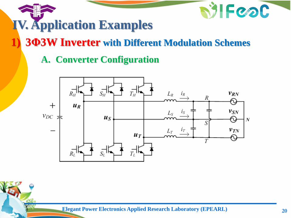
IV. Application Examples
1) 3Φ3W Inverter with Different Modulation Schemes
A. Converter Configuration
Elegant Power Electronics Applied Research Laboratory (EPEARL) 21
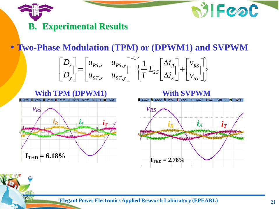
• Two-Phase Modulation (TPM) or (DPWM1) and SVPWM
iR iTiS
ITHD = 6.18%
vRS
ST
RS
S
R
S
ySTxST
yRSxRS
y
x
v
v
i
iL
Tuu
uu
D
D2
1
,,
,, 1
iTiR iS
vRS
ITHD = 2.78%
With SVPWM With TPM (DPWM1)
B. Experimental Results
Elegant Power Electronics Applied Research Laboratory (EPEARL) 22
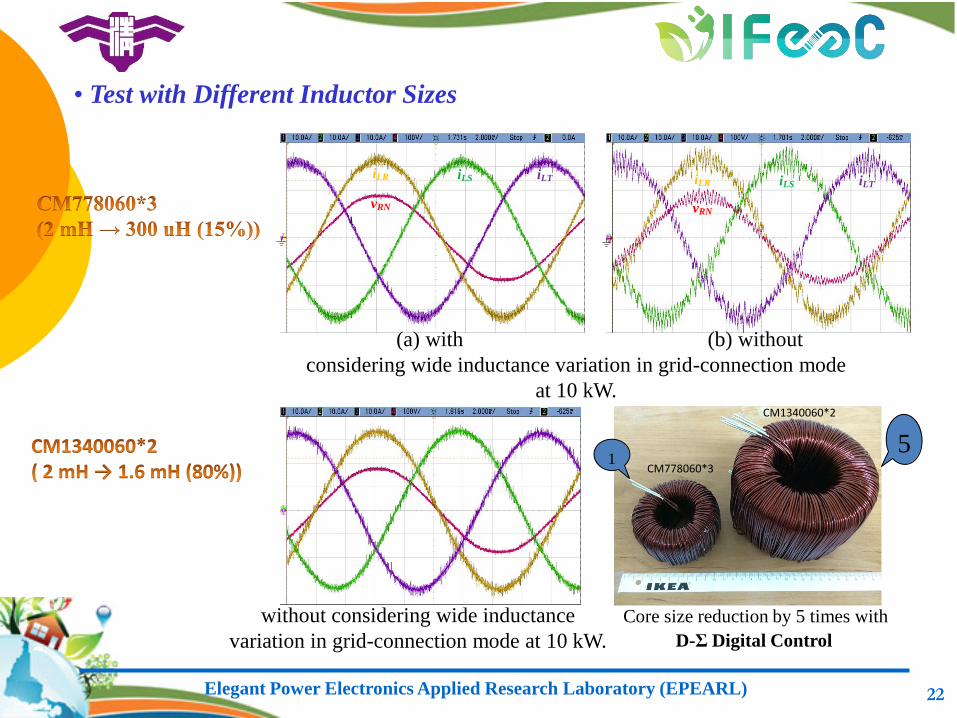
• Test with Different Inductor Sizes
iLR iLTiLS
vRN
iLR iLTiLS
vRN
(a) with (b) without
considering wide inductance variation in grid-connection mode
at 10 kW. CM1340060*2
CM778060*3
without considering wide inductance
variation in grid-connection mode at 10 kW.
5
Core size reduction by 5 times with
D-Σ Digital Control
1
Elegant Power Electronics Applied Research Laboratory (EPEARL) 23
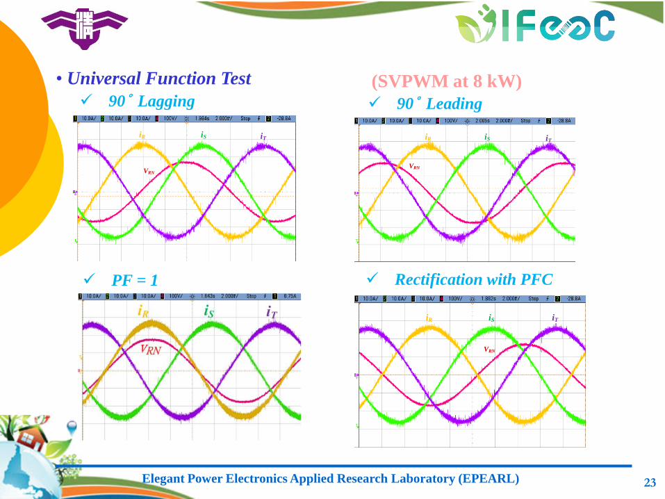
• Universal Function Test
90° Lagging 90° Leading
PF = 1 Rectification with PFC
(SVPWM at 8 kW)
VRN
iR iS iT
VRN
iR iS iT
VRN
iR iS iT
Elegant Power Electronics Applied Research Laboratory (EPEARL) 24
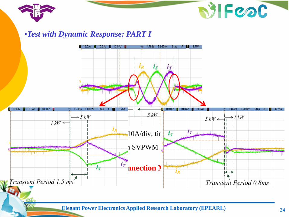
•Test with Dynamic Response: PART I
with SVPWM
(Grid-Connection Mode)
(iR, iS and iT: 10A/div; time: 5ms/div)
Elegant Power Electronics Applied Research Laboratory (EPEARL) 25
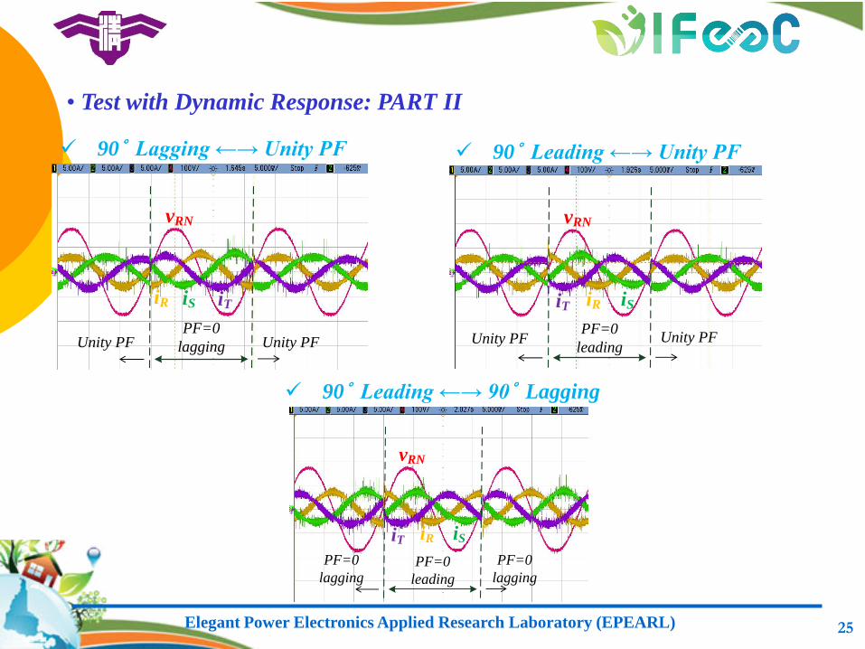
• Test with Dynamic Response: PART II
90° Lagging ←→ Unity PF 90° Leading ←→ Unity PF
90° Leading ←→ 90° Lagging
iT iR iS
Unity PFPF=0
leading
vRN
Unity PF
iTiR iS
PF=0
lagging
vRN
Unity PF Unity PF
iT iR iS
PF=0
leading
vRN
PF=0
lagging
PF=0
lagging
Elegant Power Electronics Applied Research Laboratory (EPEARL) 26
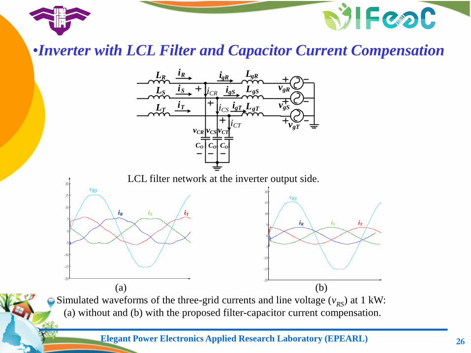
•Inverter with LCL Filter and Capacitor Current Compensation
-20
-15
-10
-5
0
5
10
15
20
vRS
iR iTiS
-20
-15
-10
-5
0
5
10
15
20
vRS
iR iTiS
(a) (b)
Simulated waveforms of the three-grid currents and line voltage (vRS) at 1 kW:
(a) without and (b) with the proposed filter-capacitor current compensation.
LR
LS
LT
iR
CO
vgT
CO CO
iS
iT
LgR
LgS
LgT
vCT
igR
iCR
iCS
iCT
igS
igT vgS
vgR
vCSvCR
LCL filter network at the inverter output side.
Elegant Power Electronics Applied Research Laboratory (EPEARL) 27
SRH
vT
LR
LS
LTvDC
uR
uS
uT
iLR
LN
uN
vS
vR
SRL
SSH STH SNH
SNLSTLSSL
CS
vRN
vSN
vTN
CS CS
vN
iLS
iLT
iLN
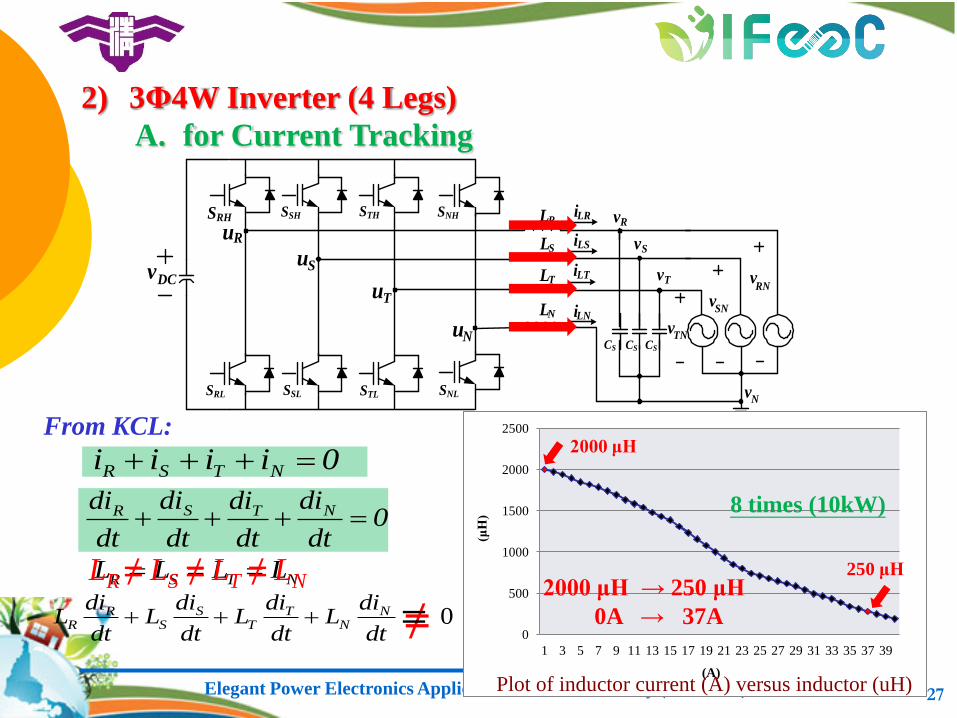
2) 3Φ4W Inverter (4 Legs)
0
500
1000
1500
2000
2500
1 3 5 7 9 11 13 15 17 19 21 23 25 27 29 31 33 35 37 39
(μH
)
(A)
0iiii NTSR
0dt
di
dt
di
dt
di
dt
di NTSR
≠ dt
diL
dt
diL
dt
diL
dt
diL N
NT
TS
SR
R 0= NTSR LLLL LR ≠ LS ≠ LT ≠ LN 2000 μH → 250 μH
0A → 37A
8 times (10kW)
250 μH
2000 μH From KCL:
Plot of inductor current (A) versus inductor (uH)
A. for Current Tracking
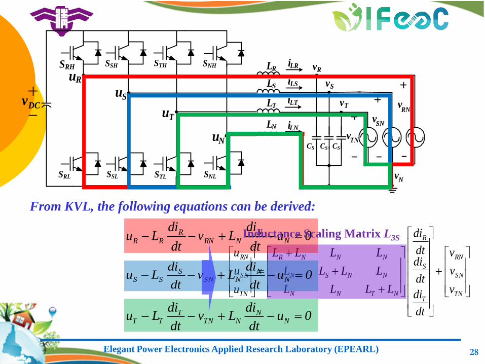
Elegant Power Electronics Applied Research Laboratory (EPEARL) 28
TN
SN
RN
T
S
R
NTNN
NNSN
NNNR
TN
SN
RN
v
v
v
dt
di
dt
didt
di
LLLL
LLLL
LLLL
u
u
u
SRH
vT
LR
LS
LTvDC
uR
uS
uT
iLR
LN
uN
vS
vR
SRL
SSH STH SNH
SNLSTLSSL
CS
vRN
vSN
vTN
CS CS
vN
iLS
iLT
iLN
0udt
diLv
dt
diLu N
NNTN
TTT
0udt
diLv
dt
diLu N
NNRN
RRR
0udt
diLv
dt
diLu N
NNSN
SSS
From KVL, the following equations can be derived:
Inductance Scaling Matrix L3S
Elegant Power Electronics Applied Research Laboratory (EPEARL) 29
v
v
v
i
i
i
dt
d
u
u
u
TN
SN
RN
T
S
R
TN
SN
RN
3SL
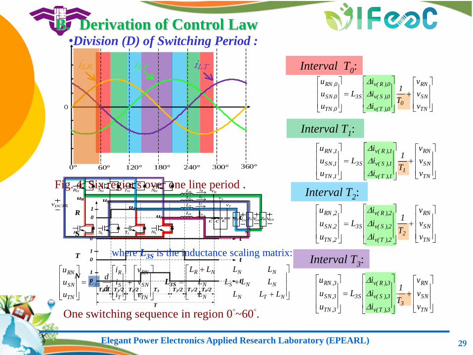
One switching sequence in region 0°~60°.
Interval T1:
Interval T0:
Interval T3:
Interval T2: Fig. 4. Six regions over one line period .
•Division (D) of Switching Period :
TN
SN
RN
22),T(v
2),S(v
2),R(v
3S
2,TN
2,SN
2,RN
v
v
v
T
1
i
i
i
L
u
u
u
TN
SN
RN
33),T(v
3),S(v
3),R(v
3S
3,TN
3,SN
3,RN
v
v
v
T
1
i
i
i
L
u
u
u
t
t
t
t
1
1
1
1
0
0
0
0
T
T0/2 T0/2T1/2 T1/2T2/2 T2/2T3
R
S
T
N
TN
SN
RN
11),T(v
1),S(v
1),R(v
3S
1,TN
1,SN
1,RN
v
v
v
T
1
i
i
i
L
u
u
u
RH
RL
SH TH
SL TL
vT
LR
LS
LTvDC
uR uS
uT
iR
iS
iT
NH
NL
LNuN
iNZRT
vS
vRN
N
ZSZ vSNv
TN
vR
C C C
where L3S is the inductance scaling matrix:
NTNN
NNSN
NNNR
LLLL
LLLL
LLLL
3SL
TN
SN
RN
00),T(v
0),S(v
0),R(v
3S
0,TN
0,SN
0,RN
v
v
v
T
1
i
i
i
L
u
u
u
0
iLSiLR
60°0° 120° 180° 300°240° 360°
iLT
B. Derivation of Control Law
Elegant Power Electronics Applied Research Laboratory (EPEARL) 30
Interval T1:
Interval T0:
Interval T3:
Interval T2:
s
TN
SN
RN
)T(v
)S(v
)R(v
1
3,TN2,TN1,TN
3,SN2,SN1,SN
3,RN2,RN1,RN
3
2
1
T
v
v
v
i
i
i
uuu
uuu
uuu
T
T
T
3SL
321S0 TTTTT
NSNRSRRNS
RNNTNRTRTN
SNTNNSNTTS
LLLLLLLLLL
LLLLLLLLLL
LLLLLLLLLL1
3S
13S
LL
0
0
0
u
u
u
0,TN
0,SN
0,RN
0
0,TN
0,SN
0,RN1-
0
TN
SN
RN1-
0),T(v
0),S(v
0),R(v
T
u
u
u
T
v
v
v
i
i
i
3S3S LL
1
1,TN
1,SN
1,RN1-
1
TN
SN
RN1-
1),T(v
1),S(v
1),R(v
T
u
u
u
T
v
v
v
i
i
i
3S3S LL
2
2,TN
2,SN
2,RN1-
2
TN
SN
RN1-
2),T(v
2),S(v
2),R(v
T
u
u
u
T
v
v
v
i
i
i
3S3S LL
3
2
1
3,RN2,TN1,TN
3,RN2,SN1,SN
3,RN2,RN1,RN1-
TN
SN
RN1-
)T(v
)S(v
)R(v
T
T
T
uuu
uuu
uuu
T
v
v
v
i
i
i
3S3S LL
3
3,TN
3,SN
3,RN1-
3
TN
SN
RN1-
3),T(v
3),S(v
3),R(v
T
u
u
u
T
v
v
v
i
i
i
3S3S LL
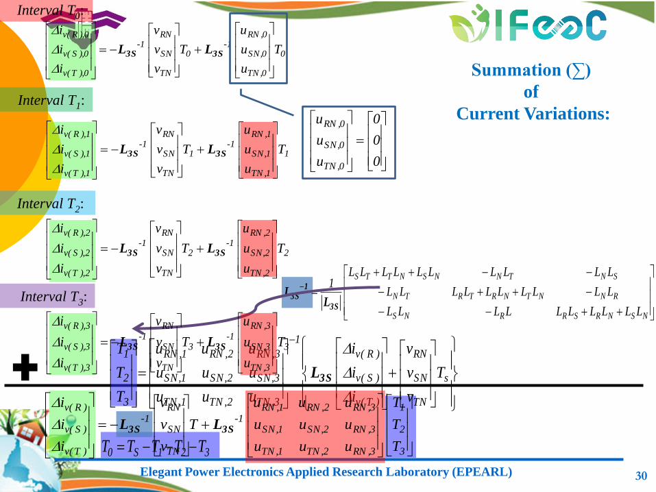
Summation (∑)
of
Current Variations:
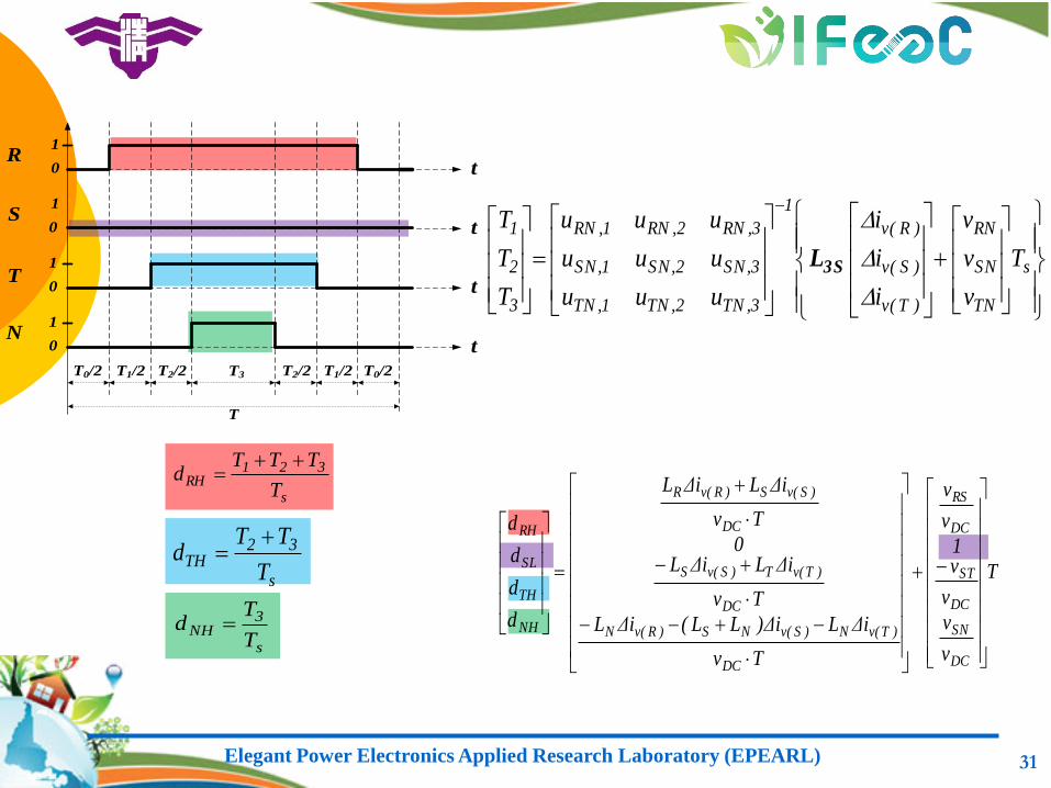
Elegant Power Electronics Applied Research Laboratory (EPEARL) 31
s
321RH
T
TTTd
s
32TH
T
TTd
s
3NH
T
Td
s
TN
SN
RN
)T(v
)S(v
)R(v
1
3,TN2,TN1,TN
3,SN2,SN1,SN
3,RN2,RN1,RN
3
2
1
T
v
v
v
i
i
i
uuu
uuu
uuu
T
T
T
3SL
t
t
t
t
1
1
1
1
0
0
0
0
T
T0/2 T0/2T1/2 T1/2T2/2 T2/2T3
R
S
T
N
T
v
v
v
v1
v
v
Tv
iΔLiΔ)LL(iΔL
Tv
iΔLiΔL0
Tv
iΔLiΔL
d
d
d
d
DC
SN
DC
ST
DC
RS
DC
)T(vN)S(vNS)R(vN
DC
)T(vT)S(vS
DC
)S(vS)R(vR
NH
TH
SL
RH
Elegant Power Electronics Applied Research Laboratory (EPEARL) 32
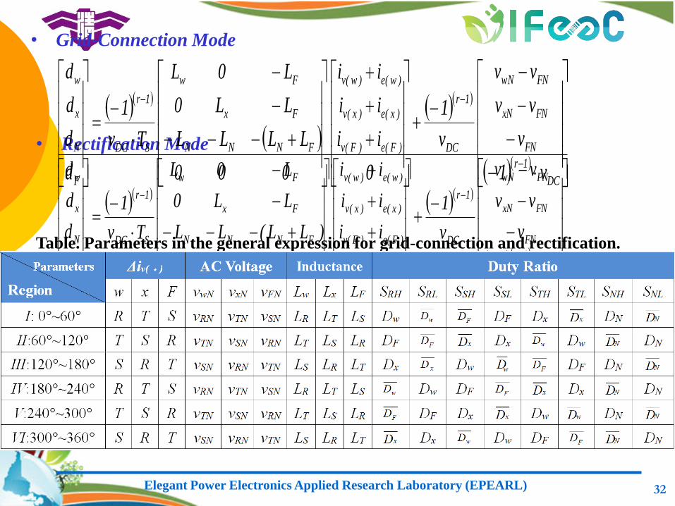
• Grid-Connection Mode
• Rectification Mode
DC
1r
FN
FNxN
FNwN
DC
1r
)F(e)F(v
)x(e)x(v
)w(e)w(v
FNNN
Fx
Fw
SDC
1r
F
N
x
w
v1
v
vv
vv
v
1
0
ii
ii
ii
000
LLLL
LL0
L0L
Tv
1
d
d
d
d
DC
1r
FN
FNxN
FNwN
DC
1r
)F(e)F(v
)x(e)x(v
)w(e)w(v
FNNN
Fx
Fw
SDC
1r
F
N
x
w
v1
v
vv
vv
v
1
0
ii
ii
ii
000
)LL(LL
LL0
L0L
Tv
1
d
d
d
d
Table. Parameters in the general expression for grid-connection and rectification.
Elegant Power Electronics Applied Research Laboratory (EPEARL) 33
TN
SN
RN
LT
LS
LR
S
s
TNTNTN
SNSNSN
RNRNRN
v
v
v
i
i
i
LT
uuu
uuu
uuu
d 3
1
3,2,1,
3,2,1,
3,2,1,
3
2
11
d
d
s
TN
SN
RN
LT
LS
LR
SS
TN
SN
RN
T
v
v
v
i
i
i
LT
u
u
u
3
s
TN
SN
RN
LT
LS
LR
S
TNTNTNTN
SNSNSNSN
RNRNRNRN
T
v
v
v
i
i
i
L
uuuu
uuuu
uuuu
3
3
2
1
0
3,2,1,0,
3,2,1,0,
3,2,1,0,
T
T
T
T
s
TN
SN
RN
LT
LS
LR
S
TNTNTN
SNSNSN
RNRNRN
T
v
v
v
i
i
i
L
uuu
uuu
uuu
3
3
2
1
3,2,1,
3,2,1,
3,2,1,
T
T
T
Interval T0 ~T4 :
• Original Mesh Equation:
t
t
t
t
1
1
1
1
0
0
0
0
TS
T0/2 T0/2T1/2 T1/2T2/2 T2/2T3
R
S
T
N
D-Σ Transformation Matrix
0
0
0
u
u
u
0,TN
0,SN
0,RN
C. Through D-Σ Transformation Matrix
Elegant Power Electronics Applied Research Laboratory (EPEARL) 34
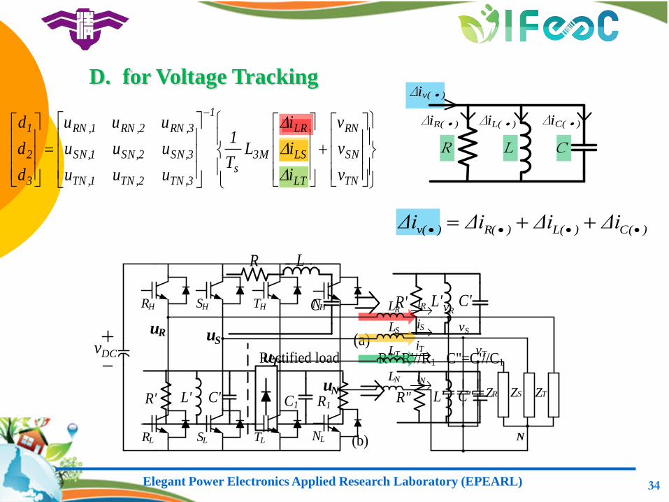
R' L' C'C
LR
(a)
C1 R1C'L'R'
R"=R'//R1 C"=C'//C1Rectified load
R" L' C"
(b)
)C()L()R()v( ΔiΔiΔi Δi
RH
RL
SH TH
SL TL
vT
LR
LS
LTvDC
uR uS
uT
iR
iS
iT
NH
NL
LNuN
iNZTZR ZS
vS
vR
N
TN
SN
RN
LT
LS
LR
M3s
1
3,TN2,TN1,TN
3,SN2,SN1,SN
3,RN2,RN1,RN
3
2
1
v
v
v
i
i
i
LT
1
uuu
uuu
uuu
d
d
d
D. for Voltage Tracking ∆iv(˙)
∆iR(˙) ∆iL(˙) ∆iC(˙)
R L C
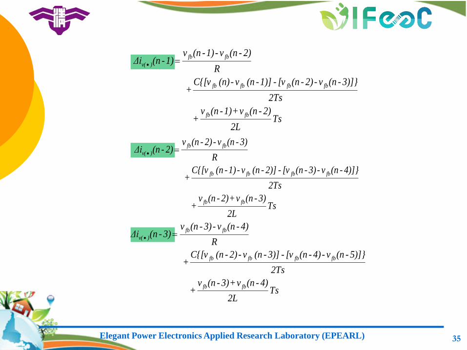
Elegant Power Electronics Applied Research Laboratory (EPEARL) 35
Ts 2L
2)-(nv+1)-(nv+
2Ts
3)]}-(nv-2)-(n[v-1)]-(n v-(n) C{[v+
R
2)-(nv-1)-(nv 1)-(nΔi
fbfb
fbfbfbfb
fbfb
)v(
Ts 2L
3)-(nv+2)-(nv+
2Ts
4)]}-(nv-3)-(n[v-2)]-(n v-1)-(n C{[v+
R
3)-(nv-2)-(nv 2)-(nΔi
fbfb
fbfbfbfb
fbfb
)v(
Ts 2L
4)-(nv+3)-(nv+
2Ts
5)]}-(nv-4)-(n[v-3)]-(n v-2)-(n C{[v+
R
4)-(nv-3)-(nv 3)-(nΔi
fbfb
fbfbfbfb
fbfb
)v(
Elegant Power Electronics Applied Research Laboratory (EPEARL) 36
L2
Ts 1)-(nΔv+
Ts2
1)-(nΔvC+
R
1)-(nΔv 1)-(nΔi LCR
)v(
L2
Ts2)-(nΔv+
Ts2
2)-(nΔvC+
R
2)-(nΔv 2)-(nΔi LCR
)v(
L2
Ts3)-(nΔv+
Ts2
3)-(nΔvC+
R
3)-(nΔv 3)-(nΔi LCR
)v(
pL
pC
pR
LCR
LCR
LCR
)(v
)(v
)(v
k
k
k
)3n(v)3n(v)3n(v
)2n(v)2n(v)2n(v
)1n(v)1n(v)1n(v
)3n(i
)2n(i
)1n(i
)3n(i
)2n(i
)1n(i
)3n(v)3n(v)3n(v
)2n(v)2n(v)2n(v
)1n(v)1n(v)1n(v
k
k
k
)(v
)(v
)(v
1
LCR
LCR
LCR
pL
pC
pR
L2
Tsk
Ts2
Ck
R
1k
pL
pC
pR
Elegant Power Electronics Applied Research Laboratory (EPEARL) 37
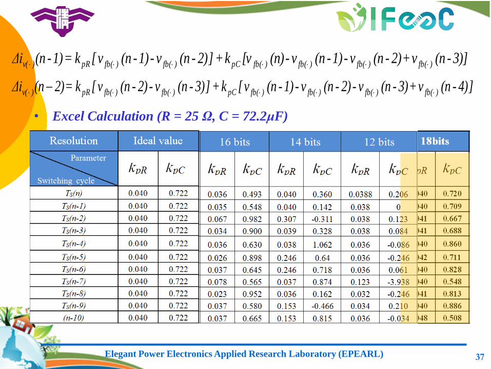
3)]-(n v+2)-(n v-1)-(n v-(n) [vk+]2)-(n v-1)-(n v[k=1)-(nΔi )fb()fb()fb()fb(pC)fb()fb(pR)v(
]4)-(n v+3)-(n v-2)-(n v-1)-(n v[k+]3)-(n v-2)-(n v[k= 2)(nΔi )fb()fb()fb()fb(pC)fb()fb(pR)v(
• Excel Calculation (R = 25 Ω, C = 72.2μF)
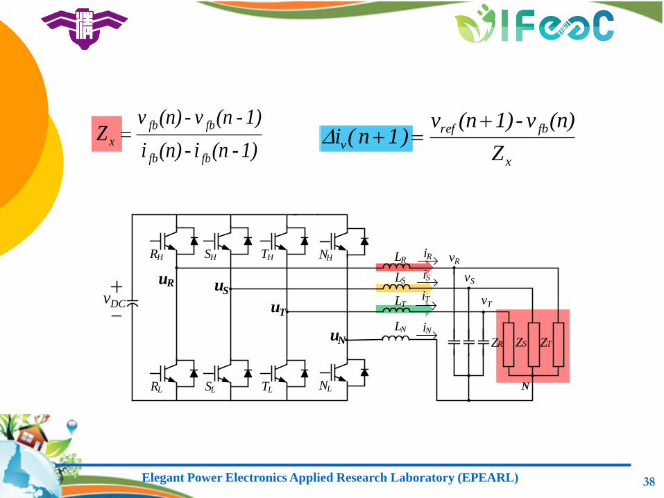
Elegant Power Electronics Applied Research Laboratory (EPEARL) 38
1)-(ni-(n)i
1)-(nv-(n)v Z
fbfb
fbfb
x
x
fbref
vZ
(n)v-1)(nv )1n(i
RH
RL
SH TH
SL TL
vT
LR
LS
LTvDC
uR uS
uT
iR
iS
iT
NH
NL
LNuN
iNZTZR ZS
vS
vR
N
Elegant Power Electronics Applied Research Laboratory (EPEARL) 39
vRN vTNvSN
iLR iLR
vRN vTNvSN
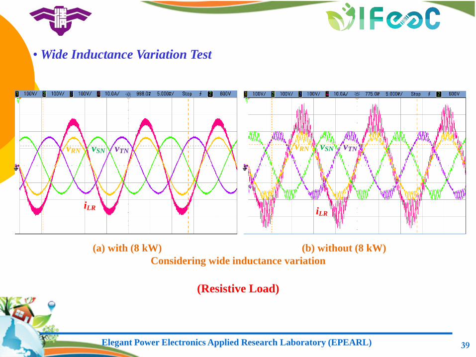
• Wide Inductance Variation Test
(a) with (8 kW) (b) without (8 kW)
Considering wide inductance variation
(Resistive Load)
Elegant Power Electronics Applied Research Laboratory (EPEARL) 40
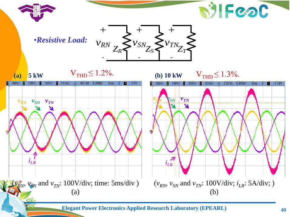
•Resistive Load:
vSN vTN vRN
(vRN, vSN and vTN: 100V/div; time: 5ms/div )
(a)
(vRN, vSN and vTN: 100V/div; iLR: 5A/div; )
(b)
(a) 5 kW
ZR ZS ZT
+
vRN
-
+
vSN
-
+
vTN
-
iLR
(b) 10 kW
vSN vTN vRN
iLR
VTHD ≤ 1.2%. VTHD ≤ 1.3%.
Elegant Power Electronics Applied Research Laboratory (EPEARL) 41
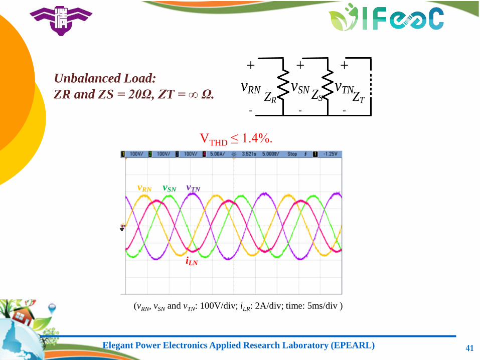
(vRN, vSN and vTN: 100V/div; iLR: 2A/div; time: 5ms/div )
Unbalanced Load:
ZR and ZS = 20Ω, ZT = ∞ Ω. ZR ZT
+
vRN
-
+
vSN
-
+
vTN
-
ZS
VTHD ≤ 1.4%.
iLN
vRN vTNvSN
Elegant Power Electronics Applied Research Laboratory (EPEARL) 42
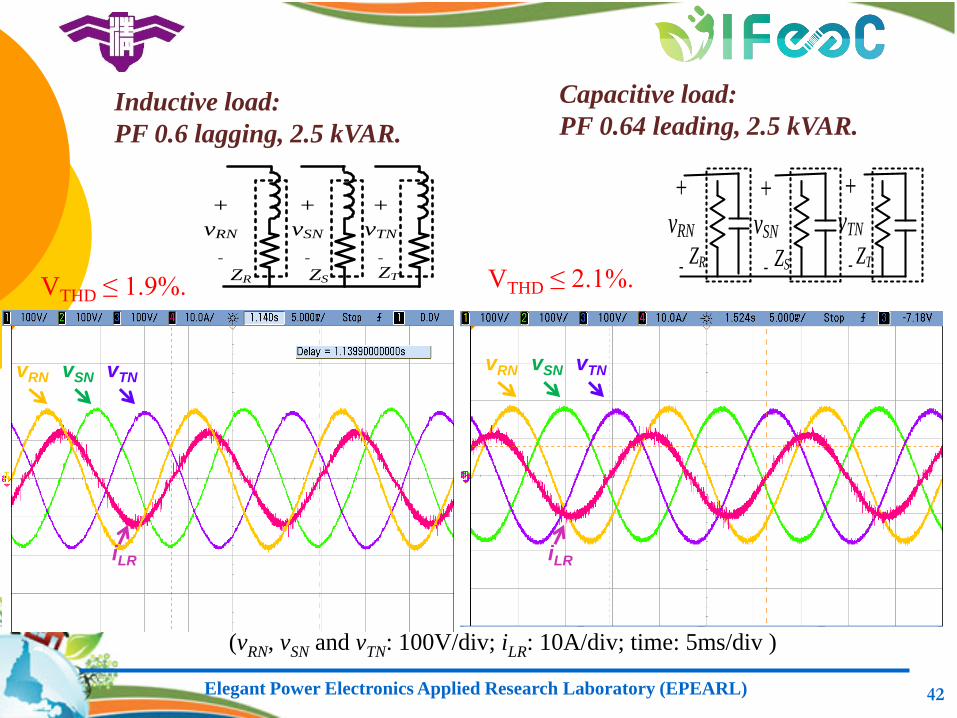
Capacitive load:
PF 0.64 leading, 2.5 kVAR.
(vRN, vSN and vTN: 100V/div; iLR: 10A/div; time: 5ms/div )
Inductive load:
PF 0.6 lagging, 2.5 kVAR.
ZR ZS ZT
+
vRN
-
+
vSN
-
+
vTN
- ZR ZS ZT
+
vRN
-
+
vSN
-
+
vTN
-
vSN vTN vRN
iLR
vSN vTN vRN
iLR
VTHD ≤ 1.9%. VTHD ≤ 2.1%.
Elegant Power Electronics Applied Research Laboratory (EPEARL) 43
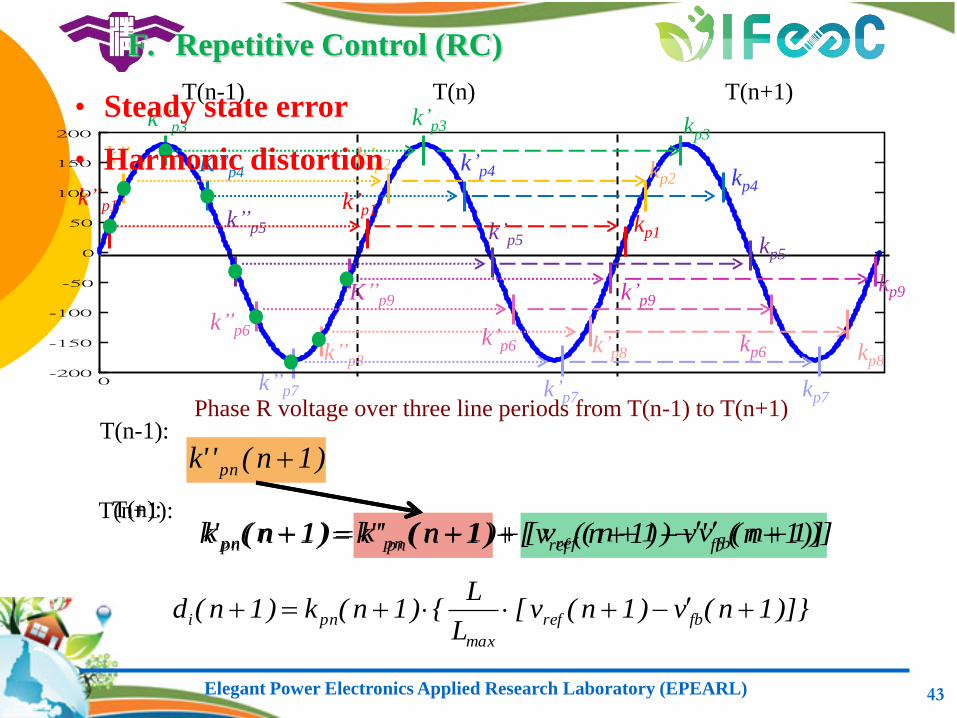
T(n): )]1n('v)1n(v[)1n(''k)1n('k fbrefpnpn
k’’p1
k’’p2
k’’p3
K’’p4
k’’p5
k’’p6
k’’p7
k’’p8
K’’p9
0-200
-150
-100
-50
0
50
100
150
200
T(n-1) T(n) T(n+1)
Phase R voltage over three line periods from T(n-1) to T(n+1)
k’p1
k’p2
k’p3
k’p4
k’p5
k’p6
k’p7
k’p8
k’p9
kp1
kp2
kp3
kp4
kp5
kp6
kp7
kp8
kp9
)1n(''k pn
‧ Steady state error
‧ Harmonic distortion
)]}1n(v)1n(v[L
L{)1n(k)1n(d fbref
max
pni
T(n-1):
)]1n(v)1n(v[)1n('k)1n(k fbrefpnpn T(n+1):
F. Repetitive Control (RC)
Elegant Power Electronics Applied Research Laboratory (EPEARL) 44
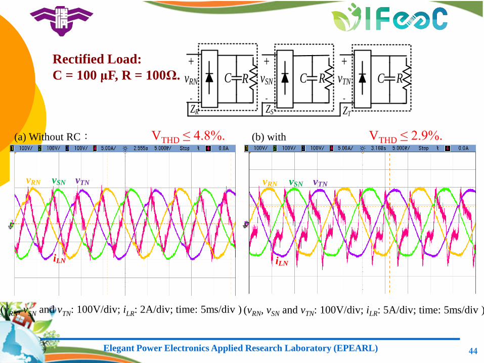
Rectified Load:
C = 100 μF, R = 100Ω.
(vRN, vSN and vTN: 100V/div; iLR: 2A/div; time: 5ms/div ) (vRN, vSN and vTN: 100V/div; iLR: 5A/div; time: 5ms/div )
(a) Without RC: (b) with
RC:
C R
+
vRN
-
C C
+
vSN
-
+
vTN
-
R R
ZR ZS ZT
VTHD ≤ 4.8%. VTHD ≤ 2.9%.
iLN
vRN vTNvSN vRN vTNvSN
iLN
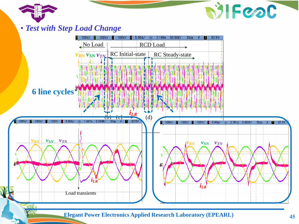
Elegant Power Electronics Applied Research Laboratory (EPEARL) 45
iLR
Load transients
RC Steady-state
No Load RCD Load
RC Initial-statevRN vTNvSN
(b) (c) (d)
iLR
vRN vTNvSN
• Test with Step Load Change
Load transients
iLR
vRN vTNvSN
6 line cycles
Elegant Power Electronics Applied Research Laboratory (EPEARL) 46
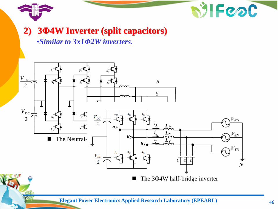
2) 3Φ4W Inverter (split capacitors)
•Similar to 3x1Φ2W inverters.
S1
S4
S7
S10
S2
S5
S8
S11
S3
S6
S9
S12
T
AC AC AC
R
S
2
D CV
2
DCV
The Neutral-point clamped (NPC) inverter
The 3Φ4W half-bridge inverter
Elegant Power Electronics Applied Research Laboratory (EPEARL) 47
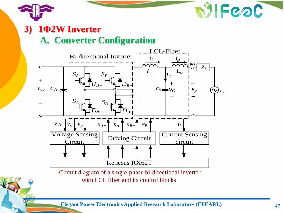
3) 1Φ2W Inverter
Circuit diagram of a single-phase bi-directional inverter
with LCL filter and its control blocks.
Ls
il
SA+ SB+
SA- SB-
DA+
DA-
DB+
DB-
vdc cdc cs vg
vdc vp
Driving Circuit
Renesas RX62T
Voltage Sensing
Circuit
Current Sensing
circuit
sA+ sA- sB+ sB- il
Lg
vC
iC
Bi-directional InverterLCL-Filter
ig
vC
Zl
vp
pcc
A. Converter Configuration
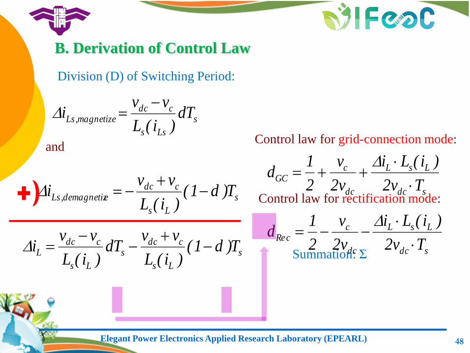
Elegant Power Electronics Applied Research Laboratory (EPEARL) 48
sdc
LsL
dc
cGC
Tv2
)i(Li
v2
v
2
1d
sdc
LsL
dc
ccRe
Tv2
)i(Li
v2
v
2
1d
Division (D) of Switching Period:
s
Lss
cdcmagnetize,Ls dT
)i(L
vvi
s
Ls
cdcedemagnetiz,Ls T)d1(
)i(L
vvi
and
s
Ls
cdcs
Ls
cdcL T)d1(
)i(L
vvdT
)i(L
vvi
Control law for grid-connection mode:
Control law for rectification mode:
B. Derivation of Control Law
Summation: Σ
Elegant Power Electronics Applied Research Laboratory (EPEARL) 49
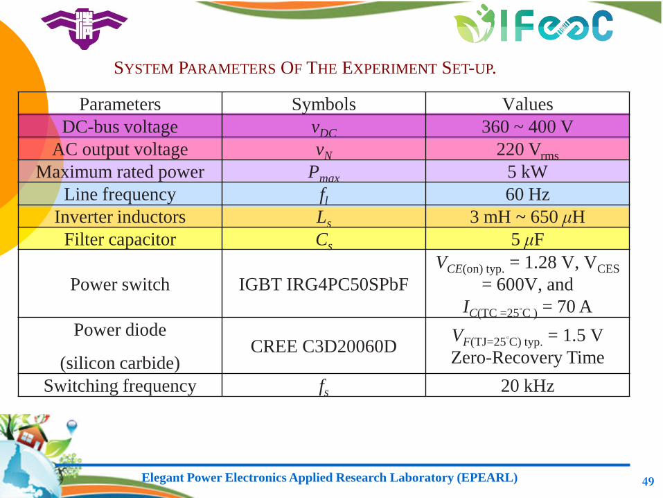
Parameters Symbols Values
DC-bus voltage vDC 360 ~ 400 V
AC output voltage vN 220 Vrms
Maximum rated power Pmax 5 kW
Line frequency fl 60 Hz
Inverter inductors Ls 3 mH ~ 650 μH
Filter capacitor Cs 5 μF
Power switch IGBT IRG4PC50SPbF
VCE(on) typ. = 1.28 V, VCES
= 600V, and
IC(TC =25°C ) = 70 A
Power diode
(silicon carbide) CREE C3D20060D
VF(TJ=25°C) typ. = 1.5 V
Zero-Recovery Time
Switching frequency fs 20 kHz
SYSTEM PARAMETERS OF THE EXPERIMENT SET-UP.
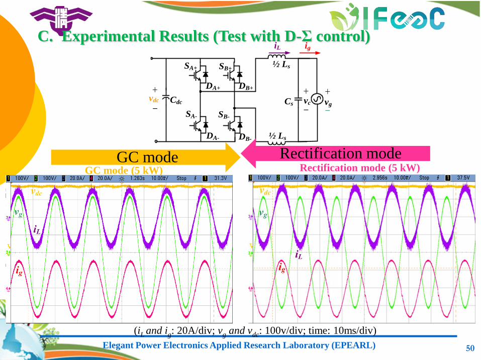
Elegant Power Electronics Applied Research Laboratory (EPEARL) 50
(iL and ig: 20A/div; vg and vdc: 100v/div; time: 10ms/div)
Rectification mode (5 kW) GC mode (5 kW)
Cdcvdc
SA+ ½ LsSB+
SA- SB-
Cs
ig
DA+
DA-
DB+
DB- ½ Ls
vg
+
_ vc
+
_
+
_
iL
Rectification mode GC mode
C. Experimental Results (Test with D-Σ control)
Elegant Power Electronics Applied Research Laboratory (EPEARL) 51
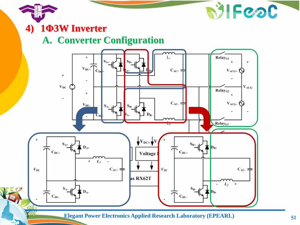
4) 1Φ3W Inverter
A. Converter Configuration
Elegant Power Electronics Applied Research Laboratory (EPEARL) 52
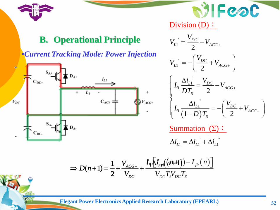
•Current Tracking Mode: Power Injection
'
1
1
"
1
1
2
1 2
DCL
ACG
S
DCL
ACG
S
ViL V
DT
ViL V
D T
"
12
DC
L ACG
VV V
'
12
DC
L ACG
VV V
Division (D):
Summation (Σ):
' "
1 1 1L L Li i i
1 11( 1)
2
ref fbACG
DC DC S
L I n I nVD n
V V T
1 1 11
( 1)2
LACG
DC DC S
L i nVD n
V V T
B. Operational Principle
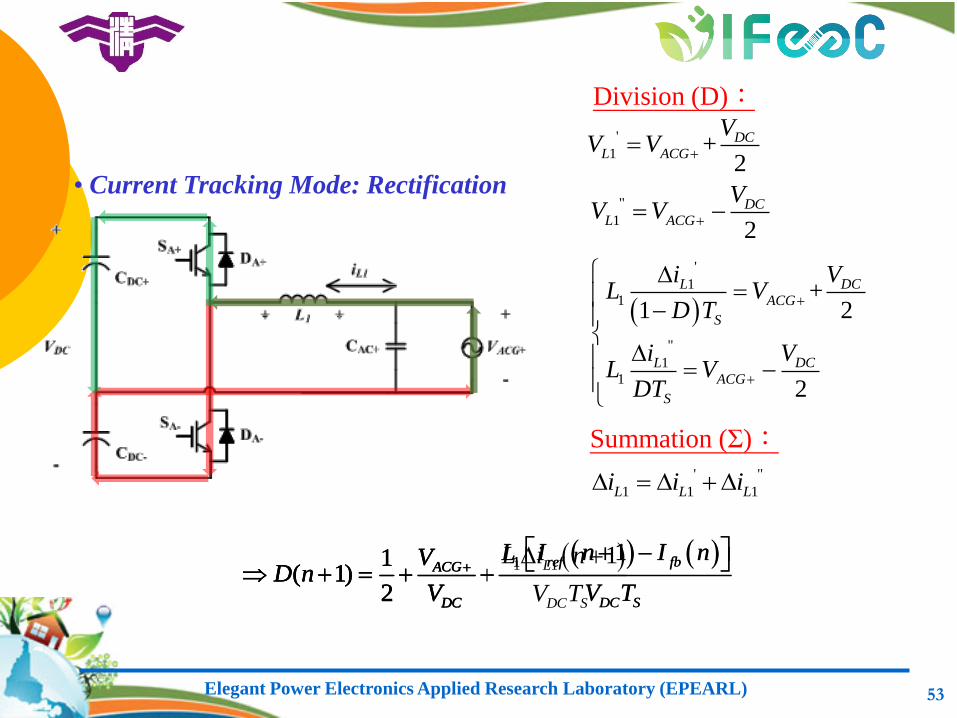
Elegant Power Electronics Applied Research Laboratory (EPEARL) 53
'
1
1
"
1
1
+1 2
2
DCL
ACG
S
DCL
ACG
S
ViL V
D T
ViL V
DT
"
12
DC
L ACG
VV V
'
1 +2
DC
L ACG
VV V
Division (D):
Summation (Σ):
' "
1 1 1L L Li i i
1 11( 1)
2
ref fbACG
DC DC S
L I n I nVD n
V V T
1 1 11
( 1)2
LACG
DC DC S
L i nVD n
V V T
1 11
( 1)2
ref fbACG
DC DC S
L I n I nVD n
V V T
• Current Tracking Mode: Rectification
Elegant Power Electronics Applied Research Laboratory (EPEARL) 54
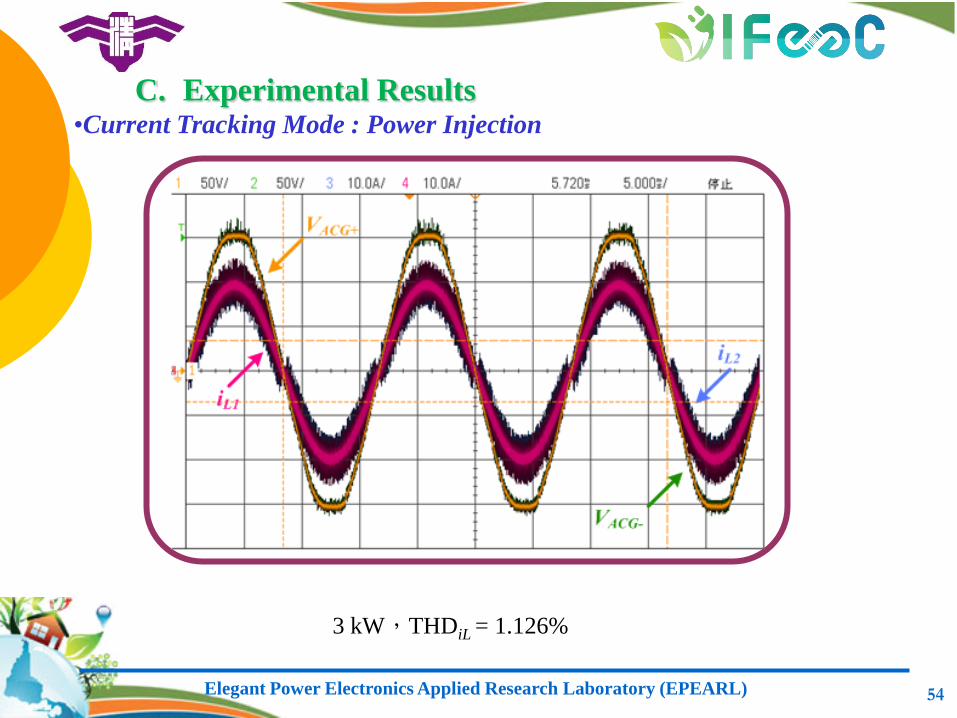
3 kW,THDiL = 1.126%
C. Experimental Results •Current Tracking Mode : Power Injection
Elegant Power Electronics Applied Research Laboratory (EPEARL) 55
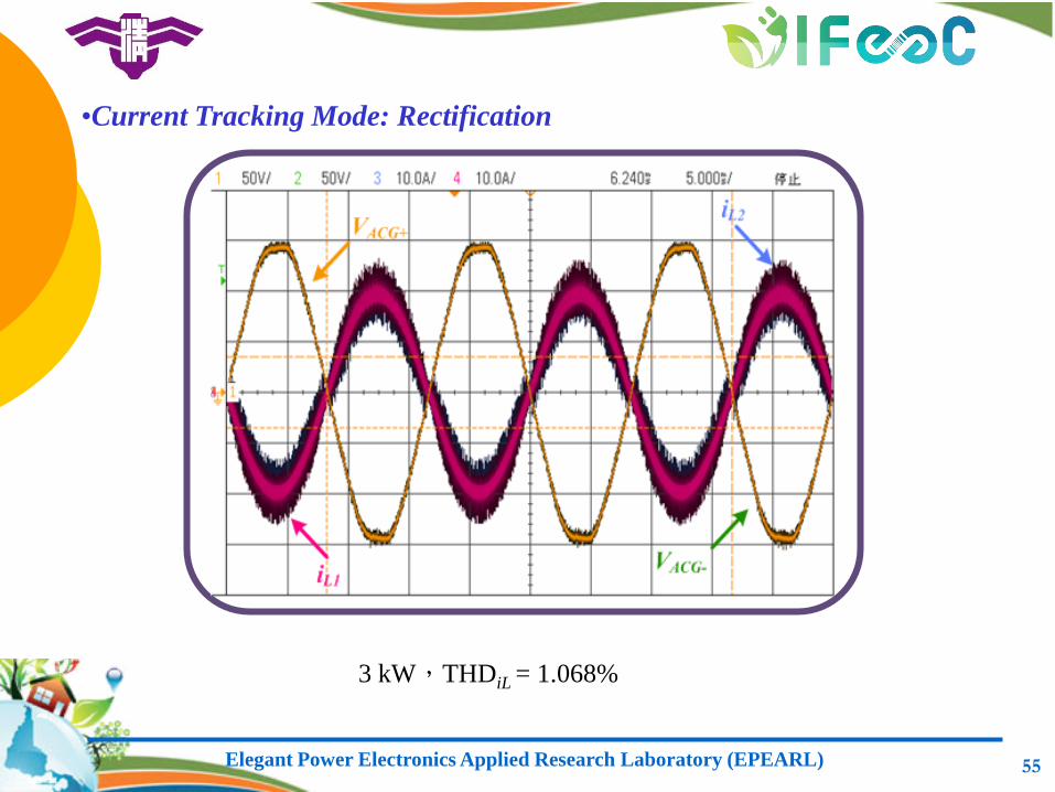
3 kW,THDiL = 1.068%
•Current Tracking Mode: Rectification
Elegant Power Electronics Applied Research Laboratory (EPEARL) 56
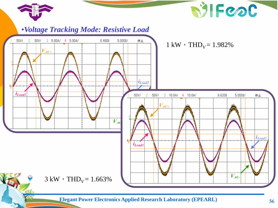
1 kW,THDV = 1.982%
3 kW,THDV = 1.663%
•Voltage Tracking Mode: Resistive Load
Elegant Power Electronics Applied Research Laboratory (EPEARL) 57
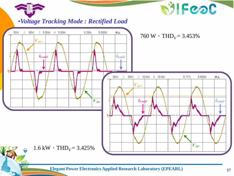
760 W,THDV = 3.453%
1.6 kW,THDV = 3.425%
•Voltage Tracking Mode : Rectified Load
Elegant Power Electronics Applied Research Laboratory (EPEARL) 58
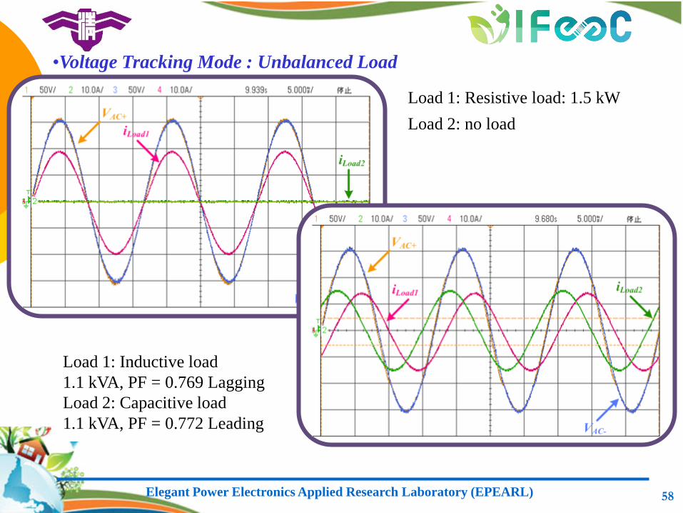
Load 1: Resistive load: 1.5 kW
Load 2: no load
Load 1: Inductive load
1.1 kVA, PF = 0.769 Lagging
Load 2: Capacitive load 1.1 kVA, PF = 0.772 Leading
•Voltage Tracking Mode : Unbalanced Load
Elegant Power Electronics Applied Research Laboratory (EPEARL) 59
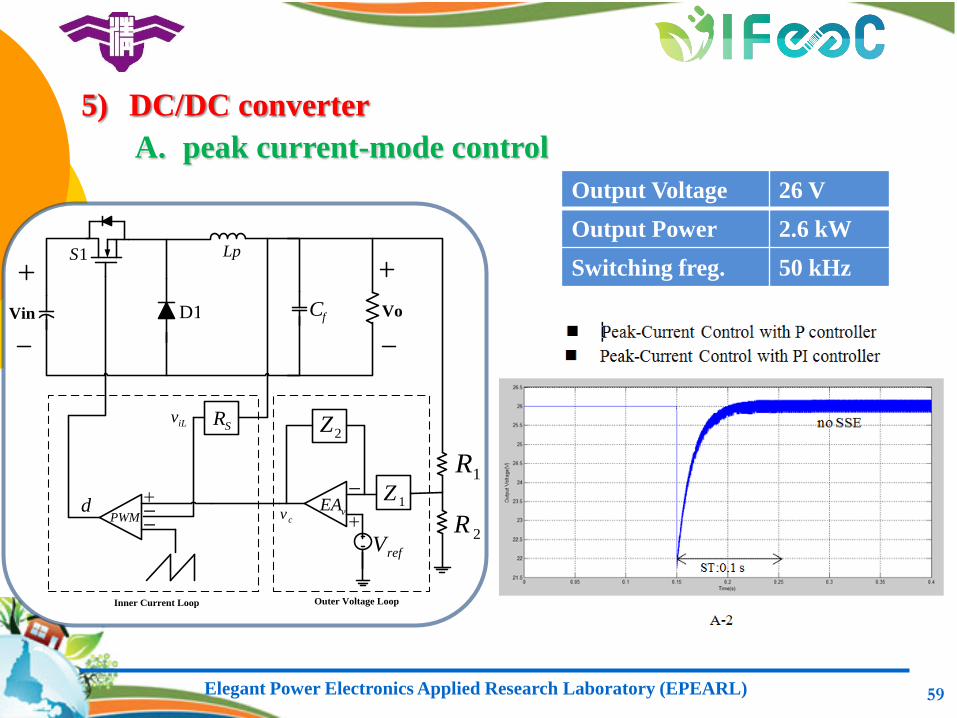
5) DC/DC converter
A. peak current-mode control
Lp1S
D1Vin
2Z
1ZvEA
refV
1R
2RPWM
SR
dcv
iLv
fC Vo
Inner Current Loop Outer Voltage Loop
Output Voltage 26 V
Output Power 2.6 kW
Switching freg. 50 kHz
Elegant Power Electronics Applied Research Laboratory (EPEARL) 60
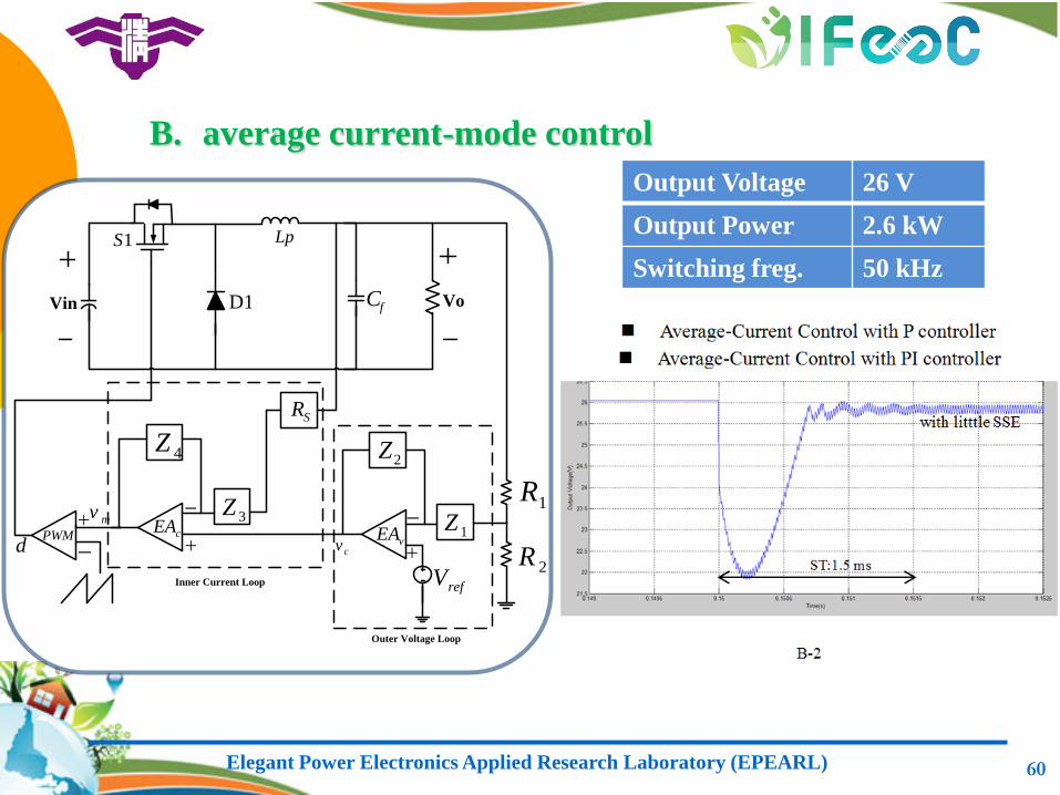
B. average current-mode control
PWM
SR
d
mv
Lp1S
D1Vin
2Z
1ZvEA
refV
1R
2Rcv
fC Vo
Outer Voltage Loop
4Z
3ZcEA
Inner Current Loop
Output Voltage 26 V
Output Power 2.6 kW
Switching freg. 50 kHz
Elegant Power Electronics Applied Research Laboratory (EPEARL) 61
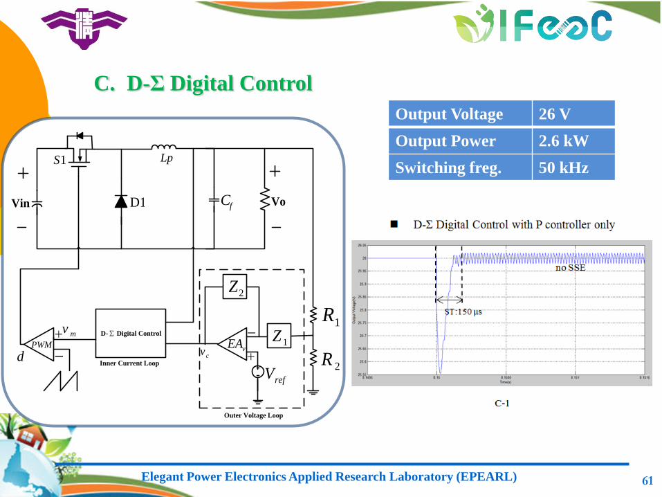
C. D-Σ Digital Control
PWM
d
mv
Lp1S
D1Vin
2Z
1ZvEA
refV
1R
2Rcv
fC Vo
Outer Voltage Loop
Inner Current Loop
D-Σ Digital Control
Output Voltage 26 V
Output Power 2.6 kW
Switching freg. 50 kHz
Elegant Power Electronics Applied Research Laboratory (EPEARL) 62
0%
20%
40%
60%
80%
100%
120%
0 5 10 15 20
Current(A)
Inductance Percentage VDC
iL
iO
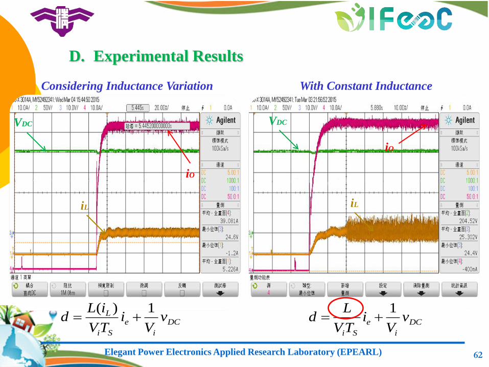
Considering Inductance Variation
DC
i
e
Si
vV
iTV
Ld
1DC
i
e
Si
L vV
iTV
iLd
1)(
VDC
iL
iO
D. Experimental Results
With Constant Inductance
Elegant Power Electronics Applied Research Laboratory (EPEARL) 63
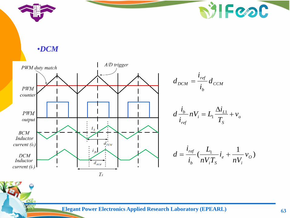
•DCM
CCM
b
ref
DCM di
id
o
S
Li
ref
b vT
iLnV
i
id
1
1
)1
( 1O
i
e
Sib
refv
nVi
TnV
L
i
id
Elegant Power Electronics Applied Research Laboratory (EPEARL) 64
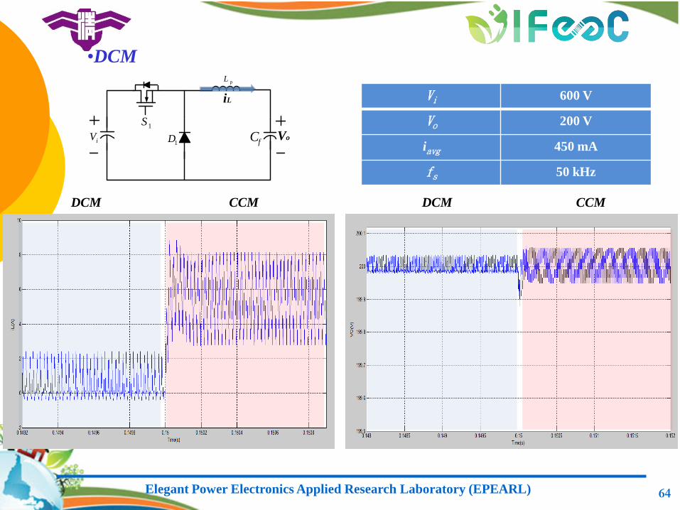
DCM CCM CCM DCM
Vi 600 V
Vo 200 V
iavg 450 mA
fs 50 kHz
1S
fC1DiV
pL
iL
Vo
•DCM
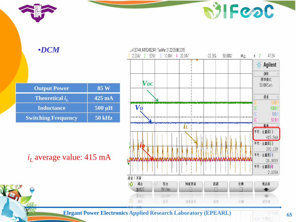
Elegant Power Electronics Applied Research Laboratory (EPEARL) 65
•DCM
VDC
VO
iL
iO
iL average value: 415 mA
Output Power 85 W
Theoretical iL 425 mA
Inductance 500 μH
Switching Frequency 50 kHz
Elegant Power Electronics Applied Research Laboratory (EPEARL) 66
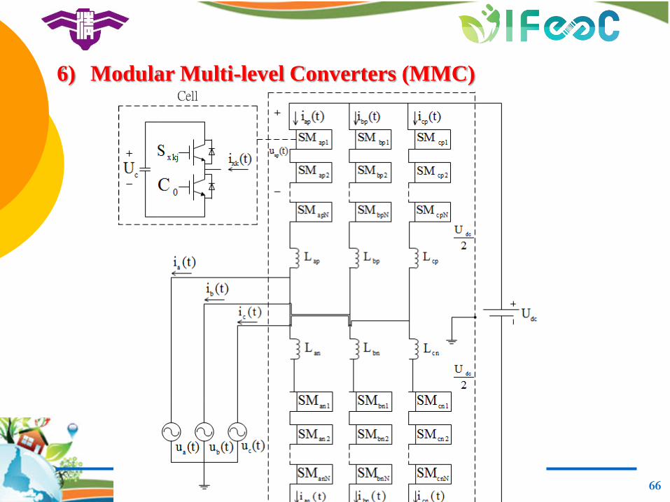
6) Modular Multi-level Converters (MMC)
Elegant Power Electronics Applied Research Laboratory (EPEARL) 67
)k(i)1k(ii
)k(i)1k(ii
)k(i)1k(ii
ccrefc
bbrefb
aarefa
cncp
cncp
c
bnbp
bnbp
b
anap
anap
a
LL
LLL
LL
LLL
LL
LLL
)120tsin(Ii
)120tsin(Ii
)tsin(Ii
Mcref
Mbref
Maref
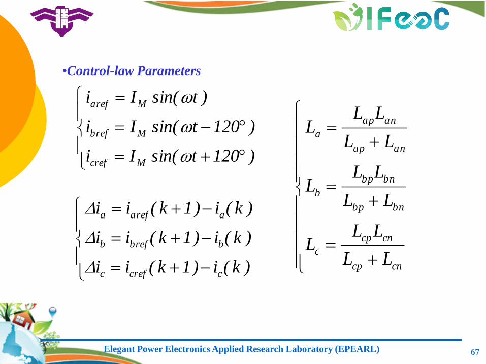
•Control-law Parameters
Elegant Power Electronics Applied Research Laboratory (EPEARL) 68
2 (2 ) ( )( ) /
2 3 3 3
( ) (2 )( ) /
2 3 3 3
2 ( 2 ) ( 2 )( ) /
2 3 3 3
ab bc a c a b c bap ap
c c cT
ab bc a c a b c bbp bp
c c cT
ab bc a c a b c bcp cp
c c cT
u u L L i L L iNN N t dt T
U U T U T
u u L L i L L iNN N t dt T
U U T U T
u u L L i L L iNN N t dt T
U U T U T
an ap
bn bp
cn cp
N N N
N N N
N N N
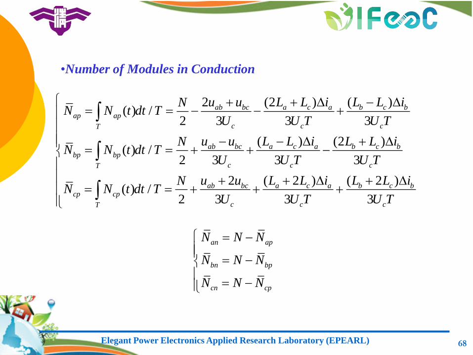
•Number of Modules in Conduction
Elegant Power Electronics Applied Research Laboratory (EPEARL) 69
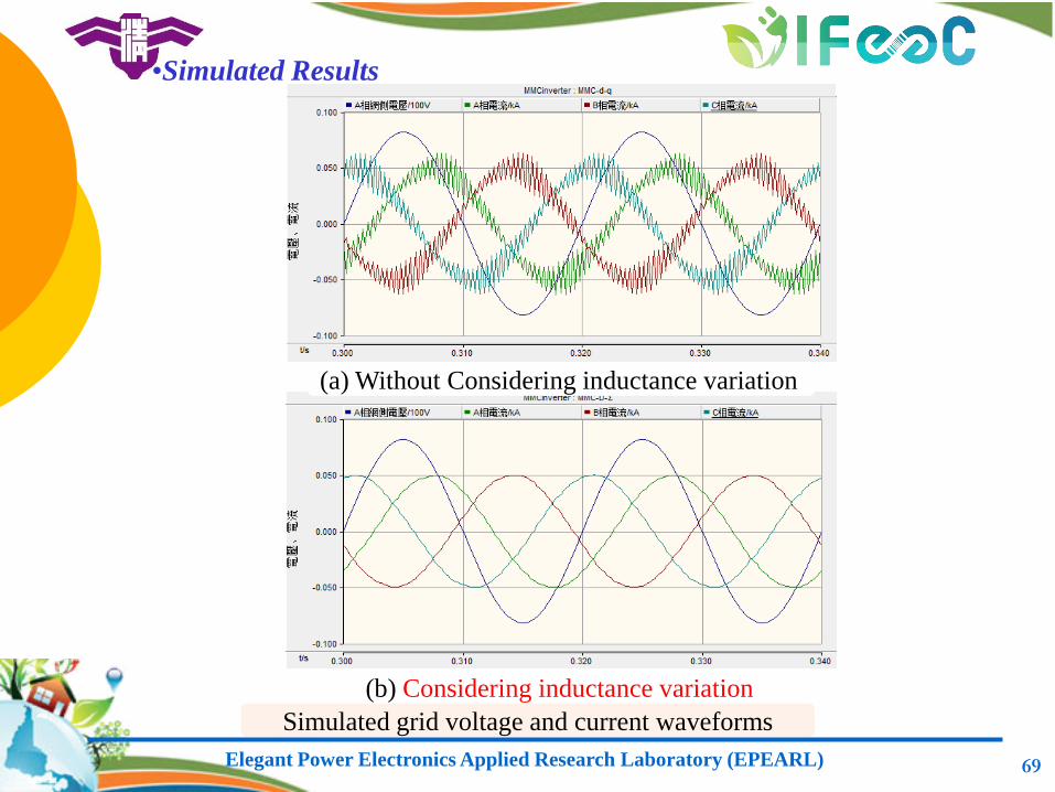
(a) Without Considering inductance variation
(b) Considering inductance variation
Simulated grid voltage and current waveforms
•Simulated Results
Elegant Power Electronics Applied Research Laboratory (EPEARL) 70
V. Conclusions D-Σ digital control is a kind of deadbeat control or
direct digital control which determines control laws
directly without frame transformation.
D-Σ digital control with a controller, which is the
inverse of plant, can accommodate the variation
effects of input voltage, switching period and filter
inductance.
With D-Σ digital control, the inverter and filter
inductor are controlled as a current source which can
achieve high stability margin even under high line
impedance.
D-Σ digital control has been successfully applied to
3Φ3W, 3Φ4W, 1Φ2W, 1Φ3W, DC/DC, and MMC
converters.
Elegant Power Electronics Applied Research Laboratory (EPEARL) 71
V. Conclusions
Future Study
1. Adopt variable switching frequency to control
ripple current or voltage under wide inductance
variation.
2. Analyze estimation error and sensitivity to
parameter changes.

Elegant Power Electronics Applied Research Laboratory (EPEARL)