
CYII5SM1300AB IBIS5 1.3 Megapixel CMOS Image Sensor Sheets/Cypress PDFs... · Global and rolling...
35
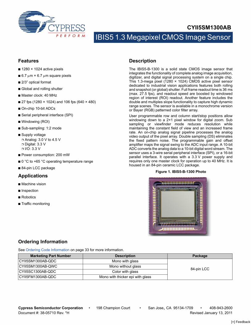
CYII5SM1300AB IBIS5 1.3 Megapixel CMOS Image Sensor Cypress Semiconductor Corporation • 198 Champion Court • San Jose, CA 95134-1709 • 408-943-2600 Document #: 38-05710 Rev. *H Revised January 13, 2011 Features ■ 1280 × 1024 active pixels ■ 6.7 μm × 6.7 μm square pixels ■ 2/3” optical format ■ Global and rolling shutter ■ Master clock: 40 MHz ■ 27 fps (1280 × 1024) and 106 fps (640 × 480) ■ On-chip 10-bit ADCs ■ Serial peripheral interface (SPI) ■ Windowing (ROI) ■ Sub-sampling: 1:2 mode ■ Supply voltage ❐ Analog: 3.0 V to 4.5 V ❐ Digital: 3.3 V ❐ I/O: 3.3 V ■ Power consumption: 200 mW ■ 0 °C to +65 °C operating temperature range ■ 84-pin LCC package Applications ■ Machine vision ■ Inspection ■ Robotics ■ Traffic monitoring Description The IBIS5-B-1300 is a solid state CMOS image sensor that integrates the functionality of complete analog image acquisition, digitizer, and digital signal processing system on a single chip. This 1.3-mega pixel (1280 × 1024) CMOS active pixel sensor dedicated to industrial vision applications features both rolling and snapshot (or global) shutter. Full frame readout time is 36 ms (max. 27.5 fps), and readout speed are boosted by windowed region of interest (ROI) readout. Another feature includes the double and multiples slope functionality to capture high dynamic range scenes. The sensor is available in a monochrome version or Bayer (RGB) patterned color filter array. User programmable row and column start/stop positions allow windowing down to a 2×1 pixel window for digital zoom. Sub sampling or viewfinder mode reduces resolution while maintaining the constant field of view and an increased frame rate. An on-chip analog signal pipeline processes the analog video output of the pixel array. Double sampling (DS) eliminates the fixed pattern noise. The programmable gain and offset amplifier maps the signal swing to the ADC input range. A 10-bit ADC converts the analog data to a 10-bit digital word stream. The sensor uses a 3-wire serial peripheral interface (SPI), or a 16-bit parallel interface. It operates with a 3.3 V power supply and requires only one master clock for operation up to 40 MHz. It is housed in an 84-pin ceramic LCC package. Figure 1. IBIS5-B-1300 Photo Ordering Information See Ordering Code Information on page 33 for more information. Marketing Part Number Description Package CYII5SM1300AB-QDC Mono with glass 84-pin LCC CYII5SM1300AB-QWC Mono without glass CYII5SC1300AB-QDC Color with glass CYII5FM1300AB-QDC Mono with thicker epi with glass [+] Feedback
Transcript of CYII5SM1300AB IBIS5 1.3 Megapixel CMOS Image Sensor Sheets/Cypress PDFs... · Global and rolling...
CYII5SM1300AB
IBIS5 1.3 Megapixel CMOS Image Sensor
Cypress Semiconductor Corporation • 198 Champion Court • San Jose, CA 95134-1709 • 408-943-2600Document #: 38-05710 Rev. *H Revised January 13, 2011
Features 1280 × 1024 active pixels
6.7 μm × 6.7 μm square pixels
2/3” optical format
Global and rolling shutter
Master clock: 40 MHz
27 fps (1280 × 1024) and 106 fps (640 × 480)
On-chip 10-bit ADCs
Serial peripheral interface (SPI)
Windowing (ROI)
Sub-sampling: 1:2 mode
Supply voltage Analog: 3.0 V to 4.5 V Digital: 3.3 V I/O: 3.3 V
Power consumption: 200 mW
0 °C to +65 °C operating temperature range
84-pin LCC package
Applications Machine vision
Inspection
Robotics
Traffic monitoring
DescriptionThe IBIS5-B-1300 is a solid state CMOS image sensor thatintegrates the functionality of complete analog image acquisition,digitizer, and digital signal processing system on a single chip.This 1.3-mega pixel (1280 × 1024) CMOS active pixel sensordedicated to industrial vision applications features both rollingand snapshot (or global) shutter. Full frame readout time is 36 ms(max. 27.5 fps), and readout speed are boosted by windowedregion of interest (ROI) readout. Another feature includes thedouble and multiples slope functionality to capture high dynamicrange scenes. The sensor is available in a monochrome versionor Bayer (RGB) patterned color filter array.User programmable row and column start/stop positions allowwindowing down to a 2×1 pixel window for digital zoom. Subsampling or viewfinder mode reduces resolution whilemaintaining the constant field of view and an increased framerate. An on-chip analog signal pipeline processes the analogvideo output of the pixel array. Double sampling (DS) eliminatesthe fixed pattern noise. The programmable gain and offsetamplifier maps the signal swing to the ADC input range. A 10-bitADC converts the analog data to a 10-bit digital word stream. Thesensor uses a 3-wire serial peripheral interface (SPI), or a 16-bitparallel interface. It operates with a 3.3 V power supply andrequires only one master clock for operation up to 40 MHz. It ishoused in an 84-pin ceramic LCC package.
Figure 1. IBIS5-B-1300 Photo
Ordering InformationSee Ordering Code Information on page 33 for more information.
Marketing Part Number Description PackageCYII5SM1300AB-QDC Mono with glass
84-pin LCCCYII5SM1300AB-QWC Mono without glassCYII5SC1300AB-QDC Color with glassCYII5FM1300AB-QDC Mono with thicker epi with glass
[+] Feedback
CYII5SM1300AB
Document #: 38-05710 Rev. *H Page 2 of 35
ContentsFeatures .................................................................................. 1Applications ........................................................................... 1Description ............................................................................. 1Ordering Information ............................................................. 1Specifications ........................................................................ 3
Key Specifications ............................................................ 3Electrical Specifications .................................................... 4
Architecture and Operation .................................................. 5Floor Plan ......................................................................... 5Pixel .................................................................................. 6Image Core Operation ...................................................... 9X-Addressing .................................................................. 11Y-addressing .................................................................. 11Output Amplifier .............................................................. 12Analog-to-Digital Converter ............................................ 13Electronic Shutter Types ................................................ 15Sequencer ...................................................................... 15
Timing Diagrams ................................................................. 20Frame Rate .................................................................... 20Timing Requirements ..................................................... 20Global Shutter: Single Slope Integration ........................ 21
Global Shutter: Pixel Readout ........................................ 22Global Shutter: Multiple Slope Integration ...................... 23Rolling Shutter Operation ............................................... 24Windowing in X-Direction ............................................... 24Windowing in Y-Direction ............................................... 25Initialization (Startup Behavior) ...................................... 25
Package Information ........................................................... 26Pin List ............................................................................ 26Pad Position and Packaging .......................................... 29Package Drawing with Glass .......................................... 30Glass Lid ........................................................................ 32
Handling Precautions .......................................................... 32Limited Warranty ................................................................. 32
Return Material Authorization (RMA) ............................. 32RoHS (Pb-free) Compliance ........................................... 32
Ordering Code Information ................................................. 33Appendix A: IBIS5 Demo Kit ............................................... 33Document History Page ...................................................... 34Sales, Solutions, and Legal Information ........................... 35
Worldwide Sales and Design Support ............................ 35
[+] Feedback
CYII5SM1300AB
Document #: 38-05710 Rev. *H Page 3 of 35
SpecificationsKey Specifications
Table 3. Recommended Operating Ratings[2]
Table 1. General Specifications
Parameter SpecificationsActive pixels 1280 (H) × 1024 (V)Pixel size 6.7 µm × 6.7µmMaster Clock 40 MHzShutter type Global and rolling shutterFrame rate 27 fps at full resolutionWindowing (ROI) Randomly programmable ROI read
out. Implemented as scanning of lines or columns from an uploaded position
ADC resolution 10-bit, on-chipExtended dynamic range Global shutter: Up to 4 slopes
Rolling shutter: Double slopePower dissipation 200 mW
Table 2. Electro Optical Specifications
Parameter SpecificationsSensitivity 8.4 V/lux.s at 650 nmFull Well Charge 62500 e-
Temporal Noise 2.5 LSB10Parasitic light sensitivity 3%Dark noise 21e-
Signal to Noise Ratio 64 dBFixed pattern noise (FPN) 4.5 LSB10Dark signal 5.5 LSB10/sec at 30 °C
Symbol Description Min Max UnitsTJ
[2] Operating temperature range 0 65 °C
TS[1] Storage temperature range 20 40 °C
Storage humidity range 30 60 %RH
Table 4. Absolute Maximum Ratings [1]
Symbol Description Min Max UnitsABS (3.0-V to 3.3-V
supply group)ABS rating for 3.0 V and 3.3 V supply group –0.5 4.3 V
ABS (4.5-V supply group) ABS rating for 4.5 V supply group –0.5 5.5 V
TS[1] ABS storage temperature range 0 150 °C
ABS storage humidity range 5 90 %RH
Electrostatic discharge (ESD)[3]
Human Body Model (HBM)See Note 4 V
Charged Device Model (CDM)LU[3] Latch-up See Note 5 mA
Notes1. Absolute maximum ratings are limits beyond which damage may occur. Long term exposure toward the maximum storage temperature accelerates color filter
degradation.2. Operating ratings are conditions in which operation of the device is intended to be functional.3. Cypress recommends that customers become familiar with, and follow the procedures in JEDEC Standard JESD625-A. Refer to Application Note AN52561. 4. The IBIS5-B-1300 complies with JESD22-A114 HBM Class 0 and JESD22-C101 Class I. It is recommended that extreme care be taken while handling these devices
to avoid damages due to ESD event. Refer to Application Note AN52561. 5. The IBIS5-B-1300 does not have latch-up protection.
[+] Feedback
CYII5SM1300AB
Document #: 38-05710 Rev. *H Page 4 of 35
Electrical Specifications
Recommended Operating Conditions
All parameters are characterized for DC conditions after thermal equilibrium is established.Always tie unused inputs to an appropriate logic level, for example, either VDD or GND.This device contains circuitry to protect the inputs against damage due to high static voltages or electric fields. However, take normalprecautions to avoid application of any voltages higher than the maximum rated voltages to this high impedance circuit.
DC Electrical Characteristics
Table 5. Recommended Operating Conditions
Parameter Description Typical Currents
Peak Currents Min Typ Max Unit
VDDH Voltage on HOLD switches. 0.047 mA 100 mA +3.3 +4.5 +4.5 VVDDR_LEFT Highest reset voltage. 0.050 mA 100 mA +3.3 +4.5 +4.5 VVDDC Pixel core voltage. 0.052 mA 100 mA +2.5 +3.0 +3.3 VVDDA Analog supply voltage of the image core. 19.265 mA N/A +3.0 +3.3 +3.6 VVDDD Digital supply voltage of the image core. 5.265 mA N/A +3.0 +3.3 +3.6 VIDDA_ADC Analog supply of ADC 34.5 mA N/A N/A N/A N/A mAIDDD_ADC Digital supply of ADC 10.5 mA N/A N/A N/A N/A mATA Commercial operating temperature. N/A N/A 0 30 65 °C
Table 6. DC Electrical Characteristics
Parameter Characteristic Condition Min Max UnitVIH Input high voltage 2.1 – VVIL Input low voltage – 0.6 VIIN Input leakage current VIN = VDD or GND –10 +10 µAVOH Output high voltage VDD = min; IOH = –100 µA 2.2 – VVOL Output low voltage VDD = min; IOH = 100 µA 0.5 VIDD Maximum operating current System clock <= 40 MHz 40 60 mA
[+] Feedback
CYII5SM1300AB
Document #: 38-05710 Rev. *H Page 5 of 35
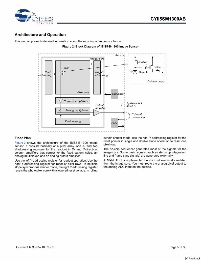
Architecture and OperationThis section presents detailed information about the most important sensor blocks
Figure 2. Block Diagram of IBIS5-B-1300 Image Sensor
Floor PlanFigure 2 shows the architecture of the IBIS5-B-1300 imagesensor. It consists basically of a pixel array, one X- and twoY-addressing registers for the readout in X- and Y-direction,column amplifiers that correct for the fixed pattern noise, ananalog multiplexer, and an analog output amplifier.Use the left Y-addressing register for readout operation. Use theright Y-addressing register for reset of pixel rows. In multipleslope synchronous shutter mode, the right Y-addressing registerresets the whole pixel core with a lowered reset voltage. In rolling
curtain shutter mode, use the right Y-addressing register for thereset pointer in single and double slope operation to reset onepixel row.The on-chip sequencer generates most of the signals for theimage core. Some basic signals (such as start/stop integration,line and frame sync signals) are generated externally. A 10-bit ADC is implemented on chip but electrically isolatedfrom the image core. You must route the analog pixel output tothe analog ADC input on the outside.
X-addressing
Analog multiplexer
Column amplifiers
Pixel core
Pixel
Output amplifier
Imager core
ADC
Sequencer
Sensor
Y-leftaddressing
Y-right addressing
External connection
System clock 40 MHz
Reset
Sample
Select
Column output
C
[+] Feedback
CYII5SM1300AB
Document #: 38-05710 Rev. *H Page 6 of 35
PixelA description of the pixel architecture and the color filter arrayfollows.
ArchitectureThe pixel architecture used in the IBIS5-B-1300 is a 4-transistorpixel as shown in Figure 3. Implement the pixel using the high fillfactor technique as patented by Cypress (US patent No.6,225,670 and others). The 4T-pixel features a snapshot shutterbut can also emulate the 3T-pixel by continuously closingsampling switch M2. Using M2 as a global sample transistor forall pixels enables the snapshot shutter mode. Due to this pixelarchitecture, integration during read out is not possible insynchronous shutter mode.
Figure 3. 4T Pixel Architecture
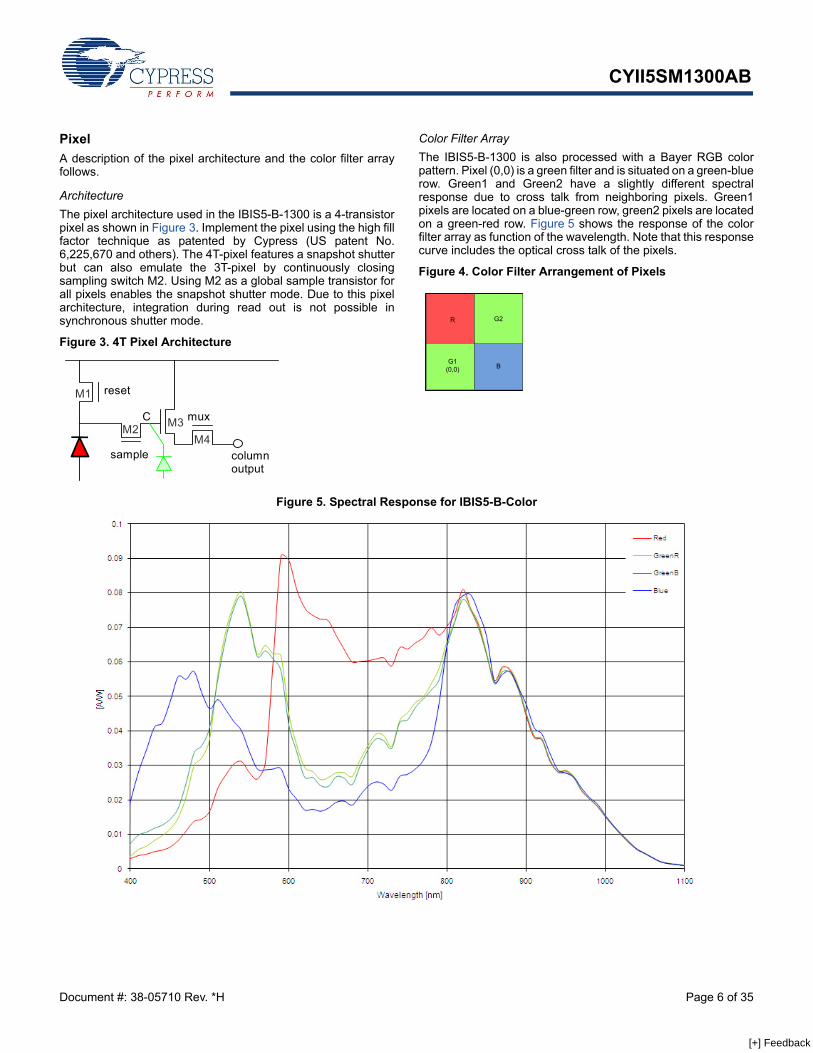
Color Filter ArrayThe IBIS5-B-1300 is also processed with a Bayer RGB colorpattern. Pixel (0,0) is a green filter and is situated on a green-bluerow. Green1 and Green2 have a slightly different spectralresponse due to cross talk from neighboring pixels. Green1pixels are located on a blue-green row, green2 pixels are locatedon a green-red row. Figure 5 shows the response of the colorfilter array as function of the wavelength. Note that this responsecurve includes the optical cross talk of the pixels.
Figure 4. Color Filter Arrangement of Pixels
Figure 5. Spectral Response for IBIS5-B-Color
reset
sample
mux
column output
C
M1
M2 M3 M4
R
G1(0,0)
G2
B
[+] Feedback
CYII5SM1300AB
Document #: 38-05710 Rev. *H Page 7 of 35
Spectral Response Curve
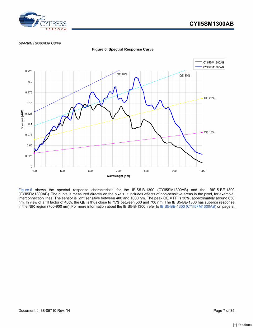
Figure 6 shows the spectral response characteristic for the IBIS5-B-1300 (CYII5SM1300AB) and the IBIS-5-BE-1300(CYII5FM1300AB). The curve is measured directly on the pixels. It includes effects of non-sensitive areas in the pixel, for example,interconnection lines. The sensor is light sensitive between 400 and 1000 nm. The peak QE × FF is 30%, approximately around 650nm. In view of a fill factor of 40%, the QE is thus close to 75% between 500 and 700 nm. The IBIS5-BE-1300 has superior responsein the NIR region (700-900 nm). For more information about the IBIS5-B-1300, refer to IBIS5-BE-1300 (CYII5FM1300AB) on page 8.
Figure 6. Spectral Response Curve
QE 10%
QE 20%
QE 30%QE 40%
0
0.025
0.05
0.075
0.1
0.125
0.15
0.175
0.2
0.225
400 500 600 700 800 900 1000
Wavelenght [nm]
Spec
res
[A/W
]
CYII5SM1300AB
CYII5FM1300AB
[+] Feedback
CYII5SM1300AB
Document #: 38-05710 Rev. *H Page 8 of 35
Electro-voltaic Response Curve
Figure 7. Electro-Voltaic Response Curve
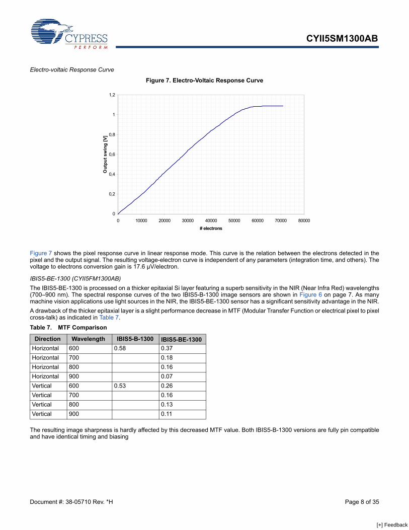
Figure 7 shows the pixel response curve in linear response mode. This curve is the relation between the electrons detected in thepixel and the output signal. The resulting voltage-electron curve is independent of any parameters (integration time, and others). Thevoltage to electrons conversion gain is 17.6 µV/electron.
IBIS5-BE-1300 (CYII5FM1300AB)The IBIS5-BE-1300 is processed on a thicker epitaxial Si layer featuring a superb sensitivity in the NIR (Near Infra Red) wavelengths(700–900 nm). The spectral response curves of the two IBIS5-B-1300 image sensors are shown in Figure 6 on page 7. As manymachine vision applications use light sources in the NIR, the IBIS5-BE-1300 sensor has a significant sensitivity advantage in the NIR.A drawback of the thicker epitaxial layer is a slight performance decrease in MTF (Modular Transfer Function or electrical pixel to pixelcross-talk) as indicated in Table 7.
The resulting image sharpness is hardly affected by this decreased MTF value. Both IBIS5-B-1300 versions are fully pin compatibleand have identical timing and biasing
Table 7. MTF Comparison
Direction Wavelength IBIS5-B-1300 IBIS5-BE-1300Horizontal 600 0.58 0.37Horizontal 700 0.18Horizontal 800 0.16Horizontal 900 0.07Vertical 600 0.53 0.26Vertical 700 0.16Vertical 800 0.13Vertical 900 0.11
0
0,2
0,4
0,6
0,8
1
1,2
0 10000 20000 30000 40000 50000 60000 70000 80000
# electrons
Out
put s
win
g [V
]
[+] Feedback
CYII5SM1300AB
Document #: 38-05710 Rev. *H Page 9 of 35
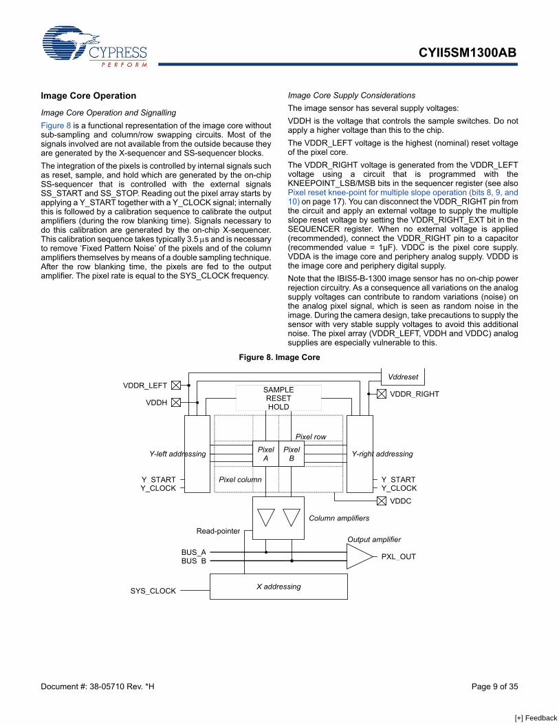
Image Core Operation
Image Core Operation and SignallingFigure 8 is a functional representation of the image core withoutsub-sampling and column/row swapping circuits. Most of thesignals involved are not available from the outside because theyare generated by the X-sequencer and SS-sequencer blocks.The integration of the pixels is controlled by internal signals suchas reset, sample, and hold which are generated by the on-chipSS-sequencer that is controlled with the external signalsSS_START and SS_STOP. Reading out the pixel array starts byapplying a Y_START together with a Y_CLOCK signal; internallythis is followed by a calibration sequence to calibrate the outputamplifiers (during the row blanking time). Signals necessary todo this calibration are generated by the on-chip X-sequencer.This calibration sequence takes typically 3.5 μs and is necessaryto remove ‘Fixed Pattern Noise’ of the pixels and of the columnamplifiers themselves by means of a double sampling technique.After the row blanking time, the pixels are fed to the outputamplifier. The pixel rate is equal to the SYS_CLOCK frequency.
Image Core Supply ConsiderationsThe image sensor has several supply voltages:VDDH is the voltage that controls the sample switches. Do notapply a higher voltage than this to the chip.The VDDR_LEFT voltage is the highest (nominal) reset voltageof the pixel core.The VDDR_RIGHT voltage is generated from the VDDR_LEFTvoltage using a circuit that is programmed with theKNEEPOINT_LSB/MSB bits in the sequencer register (see alsoPixel reset knee-point for multiple slope operation (bits 8, 9, and10) on page 17). You can disconnect the VDDR_RIGHT pin fromthe circuit and apply an external voltage to supply the multipleslope reset voltage by setting the VDDR_RIGHT_EXT bit in theSEQUENCER register. When no external voltage is applied(recommended), connect the VDDR_RIGHT pin to a capacitor(recommended value = 1µF). VDDC is the pixel core supply.VDDA is the image core and periphery analog supply. VDDD isthe image core and periphery digital supply.Note that the IBIS5-B-1300 image sensor has no on-chip powerrejection circuitry. As a consequence all variations on the analogsupply voltages can contribute to random variations (noise) onthe analog pixel signal, which is seen as random noise in theimage. During the camera design, take precautions to supply thesensor with very stable supply voltages to avoid this additionalnoise. The pixel array (VDDR_LEFT, VDDH and VDDC) analogsupplies are especially vulnerable to this.
Figure 8. Image Core
Y_START
SAMPLE
HOLD
Y_CLOCK
Y-left addressing Y-right addressing
BUS_A
Y_CLOCK
Pixel row
Pixel column
X addressing
Column amplifiers
BUS_B
SYS_CLOCK
Read-pointer
Y_START
RESETVDDH
VDDR_LEFTVDDR_RIGHT
Vddreset
VDDC
Output amplifier
PXL_OUT
Pixel A
Pixel B
[+] Feedback
CYII5SM1300AB
Document #: 38-05710 Rev. *H Page 10 of 35
Global Shutter Supply ConsiderationsThe recommended supply voltage settings listed in Table 8 areused when the IBIS5-B-1300 sensor is in global shutter modeonly.
Dual Shutter Supply ConsiderationsIf you analyze the supply settings listed in Table 8, you can seesome fixed column non-uniformities (FPN) when operating inrolling shutter mode. If a dual shutter mode (both rolling andglobal shutter) is required during operation, you must apply the
supply settings listed in Table 9 to achieve the best possibleimage quality.
Image Core Biasing SignalsTable 10 summarizes the biasing signals required to drive theIBIS5-B-1300. For optimization on speed and power dissipationof all internal blocks, several biasing resistors are needed.Each biasing signal determines the operation of a correspondingmodule in the sense that it controls the speed and power dissi-pation. The tolerance on the DC-level of the bias levels can vary±150 mV due to process variations.
Table 8. Global Shutter Recommended Supply Settings
Parameter Description Typ UnitVDDH Voltage on HOLD switches. +4.5 VVDDR_LEFT Highest reset voltage. +4.5 VVDDC Pixel core voltage. +3.3 VVDDA Analog supply voltage of the
image core. +3.3 V
VDDD Digital supply voltage of the image core.
+3.3 V
GNDA Analog ground. 0 VGNDD Digital ground. 0 VGND_AB Anti-blooming ground. 0 V
Table 9. Dual Shutter Recommended Supply Settings
Parameter Description Typ UnitVDDH Voltage on HOLD switches. +4.5 VVDDR_LEFT Highest reset voltage. +4.5 VVDDC Pixel core voltage. +3.0 VVDDA Analog supply voltage of the
image core.+3.3 V
VDDD Digital supply voltage of the image core.
+3.3 V
GNDA Analog ground. 0 VGNDD Digital ground. 0 VGND_AB Anti-blooming ground. 0 V
Table 10. Overview of Bias Signals
Signal Comment Related module DC-LevelDEC_CMD Connect to VDDA with R = 51 kΩ and decouple to GNDA with C = 100 nF. Decoder stage. 1.0 VDAC_VHIGH Connect to VDDA with R = 0Ω. High level of DAC. 3.3 VDAC_VLOW Connect to GNDA with R = 0Ω. Low level of DAC. 0.0 VAMP_CMD Connect to VDDA with R = 51 kΩ and decouple to GNDA with C = 100 nF. Output amplifier stage. 1.2 VCOL_CMD Connect to VDDA with R = 51 kΩ and decouple to GNDA with C = 100 nF. Columns amplifiers stage. 1.0 VPC_CMD Connect to VDDA with R = 22 kΩ and decouple to GNDA with C = 100 nF. Pre-charge of column
busses. 1.17 V
ADC_CMD Connect to VDDA with R = 51 kΩ and decouple to GNDA with C = 100 nF. Analog stage of ADC. 1.0 VADC_VHIGH Connect to VDDA with R = 230Ω and decouple to GNDA with C = 100 nF. High level of ADC. 2.7 VADC_VLOW Connect to GNDA with R = 410Ω and decouple to GNDA with C = 100 nF. Low level of ADC. 1.2 V
[+] Feedback
CYII5SM1300AB
Document #: 38-05710 Rev. *H Page 11 of 35
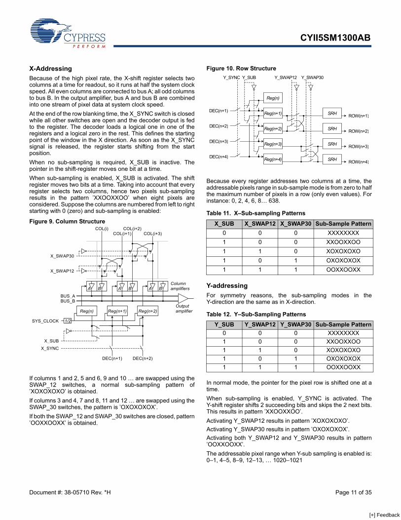
X-AddressingBecause of the high pixel rate, the X-shift register selects twocolumns at a time for readout, so it runs at half the system clockspeed. All even columns are connected to bus A; all odd columnsto bus B. In the output amplifier, bus A and bus B are combinedinto one stream of pixel data at system clock speed.At the end of the row blanking time, the X_SYNC switch is closedwhile all other switches are open and the decoder output is fedto the register. The decoder loads a logical one in one of theregisters and a logical zero in the rest. This defines the startingpoint of the window in the X direction. As soon as the X_SYNCsignal is released, the register starts shifting from the startposition.When no sub-sampling is required, X_SUB is inactive. Thepointer in the shift-register moves one bit at a time. When sub-sampling is enabled, X_SUB is activated. The shiftregister moves two bits at a time. Taking into account that everyregister selects two columns, hence two pixels sub-samplingresults in the pattern ’XXOOXXOO’ when eight pixels areconsidered. Suppose the columns are numbered from left to rightstarting with 0 (zero) and sub-sampling is enabled:
Figure 9. Column Structure
If columns 1 and 2, 5 and 6, 9 and 10 … are swapped using theSWAP_12 switches, a normal sub-sampling pattern of’XOXOXOXO’ is obtained.If columns 3 and 4, 7 and 8, 11 and 12 … are swapped using theSWAP_30 switches, the pattern is ’OXOXOXOX’.If both the SWAP_12 and SWAP_30 switches are closed, pattern’OOXXOOXX’ is obtained.
Figure 10. Row Structure
Because every register addresses two columns at a time, theaddressable pixels range in sub-sample mode is from zero to halfthe maximum number of pixels in a row (only even values). Forinstance: 0, 2, 4, 6, 8… 638.
Y-addressingFor symmetry reasons, the sub-sampling modes in theY-direction are the same as in X-direction.
In normal mode, the pointer for the pixel row is shifted one at atime.When sub-sampling is enabled, Y_SYNC is activated. TheY-shift register shifts 2 succeeding bits and skips the 2 next bits.This results in pattern ’XXOOXXOO’.Activating Y_SWAP12 results in pattern ’XOXOXOXO’. Activating Y_SWAP30 results in pattern ’OXOXOXOX’. Activating both Y_SWAP12 and Y_SWAP30 results in pattern’OOXXOOXX’.The addressable pixel range when Y-sub sampling is enabled is:0–1, 4–5, 8–9, 12–13, … 1020–1021
Reg(n+1) Reg(n+2) Reg(n)
X_SYNC
X_SUB
A B A B Column amplifiers BA
BUS_ABUS_B
X_SWAP30
X_SWAP12
COL(i) COL(i+2) COL(i+1) COL(i+3)
DEC(n+1) DEC(n+2)
1/2 SYS_CLOCK
Output amplifier
Table 11. X–Sub-sampling Patterns
X_SUB X_SWAP12 X_SWAP30 Sub-Sample Pattern0 0 0 XXXXXXXX1 0 0 XXOOXXOO1 1 0 XOXOXOXO1 0 1 OXOXOXOX1 1 1 OOXXOOXX
Table 12. Y–Sub-Sampling PatternsY_SUB Y_SWAP12 Y_SWAP30 Sub-Sample Pattern
0 0 0 XXXXXXXX1 0 0 XXOOXXOO1 1 0 XOXOXOXO1 0 1 OXOXOXOX1 1 1 OOXXOOXX
Reg(n)
Reg(n+1)
Reg(n+2)
Reg(n+3)
Reg(n+4)
Y_SWAP12
SRH
SRH
SRH
SRH
ROW(n+1)
ROW(n+2)
ROW(n+3)
ROW(n+4)
Y_SWAP30Y_SYNC Y_SUB
DEC(n+1)
DEC(n+2)
DEC(n+3)
DEC(n+4)
[+] Feedback
CYII5SM1300AB
Document #: 38-05710 Rev. *H Page 12 of 35
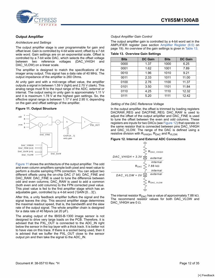
Output AmplifierArchitecture and SettingsThe output amplifier stage is user programmable for gain andoffset level. Gain is controlled by 4-bit wide word; offset by a 7-bitwide word. Gain settings are on an exponential scale. Offset iscontrolled by a 7-bit wide DAC, which selects the offset voltagebetween two reference voltages (DAC_VHIGH andDAC_VLOW) on a linear scale. The amplifier is designed to match the specifications of theimager array output. This signal has a data rate of 40 MHz. Theoutput impedance of the amplifier is 260 Ohms. At unity gain and with a mid-range offset value, the amplifieroutputs a signal in between 1.59 V (light) and 2.70 V (dark). Thisanalog range must fit to the input range of the ADC, external orinternal. The output swing in unity gain is approximately 1.11 Vand it is maximum 1.78 V at the highest gain settings. So, theeffective signal range is between 1.17 V and 2.95 V, dependingon the gain and offset settings of the amplifier.
Figure 11. Output Structure
Figure 11 shows the architecture of the output amplifier. The oddand even column amplifiers sample both pixel and reset value toperform a double sampling FPN correction. You can adjust twodifferent offsets using the on-chip DAC (7 bit): DAC_FINE andDAC_RAW. DAC_FINE is used to tune the difference betweenodd and even columns; DAC_RAW is used to add a common(both even and odd columns) to the FPN corrected pixel value.This pixel value is fed to the first amplifier stage which has anadjustable gain, controlled by a 4-bit word (’GAIN [0…3]’). After this, a unity feedback amplifier buffers the signal and thesignal leaves the chip. This second amplifier stage determinesthe maximal readout speed, that is, the bandwidth and the slewrate of the output signal. The whole amplifier chain is designedfor a data rate of 40 Mpix/s (at 20 pF).The analog output of the IBIS5-B-1300 image sensor is notdesigned to drive very large loads on the PCB. Therefore, it isadvised that the PXL_OUT is connected to the ADC_IN rightbelow the sensor in the top layer with a thick track. It is better notto have vias on this trace. If there is a socket being used, then itis advised that we buffer the PXL_OUT close to the sensoroutput pin and then take the signal to the ADC_IN.
Output Amplifier Gain Control The output amplifier gain is controlled by a 4-bit word set in theAMPLIFIER register (see section Amplifier Register (6:0) onpage 19). An overview of the gain settings is given in Table 13.
Setting of the DAC Reference VoltageIn the output amplifier, the offset is trimmed by loading registersDACRAW_REG and DACFINE_REG. DAC_RAW is used toadjust the offset of the output amplifier and DAC_FINE is usedto tune the offset between the even and odd columns. Theseregisters are inputs for two DACs (see Figure 12) that operate onthe same resistor that is connected between pins DAC_VHIGHand DAC_VLOW. The range of the DAC is defined using aresistive division with RVHIGH, RDAC and RVLOW.
Figure 12. Internal and External ADC Connections
The internal resistor RDAC has a value of approximately 7.88 kΩ.The recommend resistor values for both DAC_VLOW andDAC_VHIGH are 0 Ω.
A
GAIN [0…3] unity gain
1
S R
S
R
odd
even + +
DAC_VHIGH
DAC_VLOW DAC_RAW [6:0] DAC_FINE [6:0]
DAC_RAW
DAC_FINE
PXL_OUT
Table 13. Overview Gain SettingsBits DC Gain Bits DC Gain0000 1.37 1000 6.250001 1.62 1001 7.890010 1.96 1010 9.210011 2.33 1011 11.000100 2.76 1100 11.370101 3.50 1101 11.840110 4.25 1110 12.320111 5.20 1111 12.42
RDAC_VHIGH
DAC_VLOW = 0V
DAC_VHIGH = 3.3V
RDAC_VLOW
RDAC
externalinternal
external
7.88 kΩ internal
[+] Feedback
CYII5SM1300AB
Document #: 38-05710 Rev. *H Page 13 of 35
Analog-to-Digital ConverterThe IBIS5-B-1300 has a 10-bit flash analog digital converterrunning nominally at 40 Msamples/s. The ADC is electricallyseparated from the image sensor. Tie the input of the ADC(ADC_IN; pin 69) externally to the output (PXL_OUT1; pin 28) ofthe output amplifier.
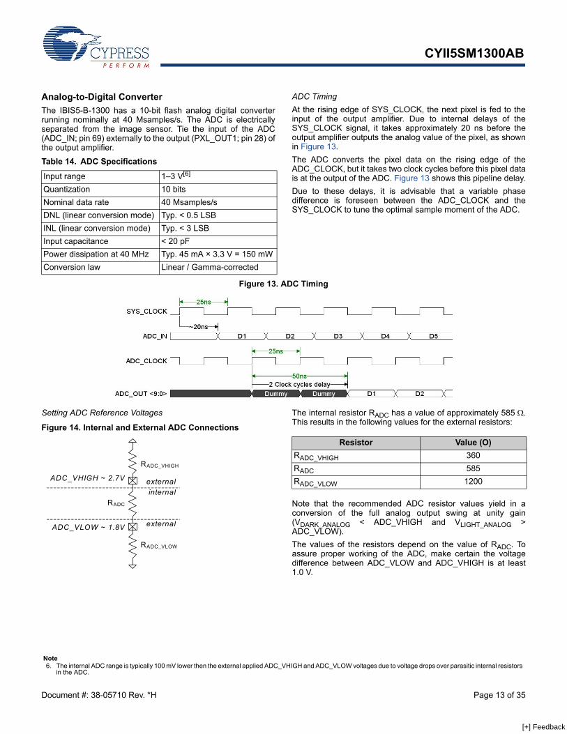
ADC TimingAt the rising edge of SYS_CLOCK, the next pixel is fed to theinput of the output amplifier. Due to internal delays of theSYS_CLOCK signal, it takes approximately 20 ns before theoutput amplifier outputs the analog value of the pixel, as shownin Figure 13. The ADC converts the pixel data on the rising edge of theADC_CLOCK, but it takes two clock cycles before this pixel datais at the output of the ADC. Figure 13 shows this pipeline delay.Due to these delays, it is advisable that a variable phasedifference is foreseen between the ADC_CLOCK and theSYS_CLOCK to tune the optimal sample moment of the ADC.
Figure 13. ADC Timing
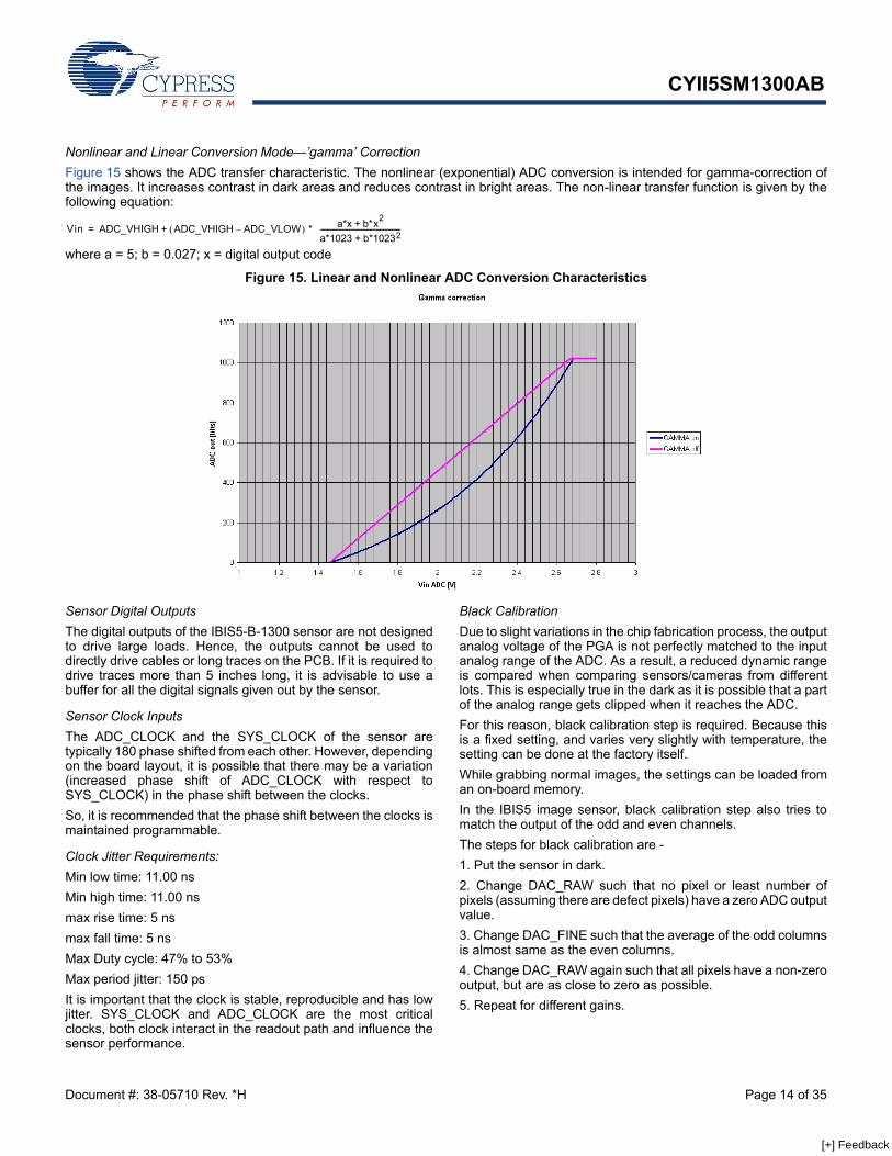
Setting ADC Reference Voltages
Figure 14. Internal and External ADC Connections
The internal resistor RADC has a value of approximately 585 Ω.This results in the following values for the external resistors:
Note that the recommended ADC resistor values yield in aconversion of the full analog output swing at unity gain(VDARK_ANALOG < ADC_VHIGH and VLIGHT_ANALOG >ADC_VLOW). The values of the resistors depend on the value of RADC. Toassure proper working of the ADC, make certain the voltagedifference between ADC_VLOW and ADC_VHIGH is at least1.0 V.
Table 14. ADC Specifications
Input range 1–3 V[6]
Quantization 10 bitsNominal data rate 40 Msamples/s DNL (linear conversion mode) Typ. < 0.5 LSBINL (linear conversion mode) Typ. < 3 LSBInput capacitance < 20 pFPower dissipation at 40 MHz Typ. 45 mA × 3.3 V = 150 mW Conversion law Linear / Gamma-corrected
Note6. The internal ADC range is typically 100 mV lower then the external applied ADC_VHIGH and ADC_VLOW voltages due to voltage drops over parasitic internal resistors
in the ADC.
RADC_VHIGH
ADC_VLOW ~ 1.8V
ADC_VHIGH ~ 2.7V
RADC_VLOW
RADC
externalinternal
external
Resistor Value (O)RADC_VHIGH 360RADC 585RADC_VLOW 1200
[+] Feedback
CYII5SM1300AB
Document #: 38-05710 Rev. *H Page 14 of 35
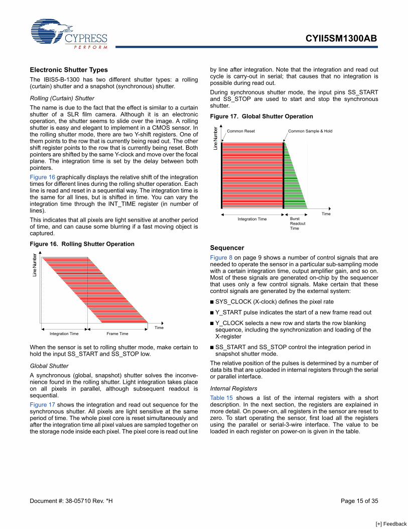
Nonlinear and Linear Conversion Mode—’gamma’ CorrectionFigure 15 shows the ADC transfer characteristic. The nonlinear (exponential) ADC conversion is intended for gamma-correction ofthe images. It increases contrast in dark areas and reduces contrast in bright areas. The non-linear transfer function is given by thefollowing equation:
where a = 5; b = 0.027; x = digital output code
Figure 15. Linear and Nonlinear ADC Conversion Characteristics
Sensor Digital OutputsThe digital outputs of the IBIS5-B-1300 sensor are not designedto drive large loads. Hence, the outputs cannot be used todirectly drive cables or long traces on the PCB. If it is required todrive traces more than 5 inches long, it is advisable to use abuffer for all the digital signals given out by the sensor.
Sensor Clock InputsThe ADC_CLOCK and the SYS_CLOCK of the sensor aretypically 180 phase shifted from each other. However, dependingon the board layout, it is possible that there may be a variation(increased phase shift of ADC_CLOCK with respect toSYS_CLOCK) in the phase shift between the clocks. So, it is recommended that the phase shift between the clocks ismaintained programmable.
Clock Jitter Requirements:Min low time: 11.00 nsMin high time: 11.00 nsmax rise time: 5 ns max fall time: 5 nsMax Duty cycle: 47% to 53%Max period jitter: 150 psIt is important that the clock is stable, reproducible and has lowjitter. SYS_CLOCK and ADC_CLOCK are the most criticalclocks, both clock interact in the readout path and influence thesensor performance.
Black CalibrationDue to slight variations in the chip fabrication process, the outputanalog voltage of the PGA is not perfectly matched to the inputanalog range of the ADC. As a result, a reduced dynamic rangeis compared when comparing sensors/cameras from differentlots. This is especially true in the dark as it is possible that a partof the analog range gets clipped when it reaches the ADC.For this reason, black calibration step is required. Because thisis a fixed setting, and varies very slightly with temperature, thesetting can be done at the factory itself.While grabbing normal images, the settings can be loaded froman on-board memory.In the IBIS5 image sensor, black calibration step also tries tomatch the output of the odd and even channels.The steps for black calibration are -1. Put the sensor in dark.2. Change DAC_RAW such that no pixel or least number ofpixels (assuming there are defect pixels) have a zero ADC outputvalue.3. Change DAC_FINE such that the average of the odd columnsis almost same as the even columns.4. Change DAC_RAW again such that all pixels have a non-zerooutput, but are as close to zero as possible.5. Repeat for different gains.
Vin ADC_VHIGH ADC_VHIGH ADC_VLOW–( ) * a*x b*x2+a*1023 b*10232+-----------------------------------------------+=
[+] Feedback
CYII5SM1300AB
Document #: 38-05710 Rev. *H Page 15 of 35
Electronic Shutter TypesThe IBIS5-B-1300 has two different shutter types: a rolling(curtain) shutter and a snapshot (synchronous) shutter.
Rolling (Curtain) ShutterThe name is due to the fact that the effect is similar to a curtainshutter of a SLR film camera. Although it is an electronicoperation, the shutter seems to slide over the image. A rollingshutter is easy and elegant to implement in a CMOS sensor. Inthe rolling shutter mode, there are two Y-shift registers. One ofthem points to the row that is currently being read out. The othershift register points to the row that is currently being reset. Bothpointers are shifted by the same Y-clock and move over the focalplane. The integration time is set by the delay between bothpointers.Figure 16 graphically displays the relative shift of the integrationtimes for different lines during the rolling shutter operation. Eachline is read and reset in a sequential way. The integration time isthe same for all lines, but is shifted in time. You can vary theintegration time through the INT_TIME register (in number oflines).This indicates that all pixels are light sensitive at another periodof time, and can cause some blurring if a fast moving object iscaptured.
Figure 16. Rolling Shutter Operation
When the sensor is set to rolling shutter mode, make certain tohold the input SS_START and SS_STOP low.
Global ShutterA synchronous (global, snapshot) shutter solves the inconve-nience found in the rolling shutter. Light integration takes placeon all pixels in parallel, although subsequent readout issequential. Figure 17 shows the integration and read out sequence for thesynchronous shutter. All pixels are light sensitive at the sameperiod of time. The whole pixel core is reset simultaneously andafter the integration time all pixel values are sampled together onthe storage node inside each pixel. The pixel core is read out line
by line after integration. Note that the integration and read outcycle is carry-out in serial; that causes that no integration ispossible during read out.During synchronous shutter mode, the input pins SS_STARTand SS_STOP are used to start and stop the synchronousshutter.
Figure 17. Global Shutter Operation
SequencerFigure 8 on page 9 shows a number of control signals that areneeded to operate the sensor in a particular sub-sampling modewith a certain integration time, output amplifier gain, and so on.Most of these signals are generated on-chip by the sequencerthat uses only a few control signals. Make certain that thesecontrol signals are generated by the external system:
SYS_CLOCK (X-clock) defines the pixel rate
Y_START pulse indicates the start of a new frame read out
Y_CLOCK selects a new row and starts the row blanking sequence, including the synchronization and loading of the X-register
SS_START and SS_STOP control the integration period in snapshot shutter mode.
The relative position of the pulses is determined by a number ofdata bits that are uploaded in internal registers through the serialor parallel interface.
Internal RegistersTable 15 shows a list of the internal registers with a shortdescription. In the next section, the registers are explained inmore detail. On power-on, all registers in the sensor are reset tozero. To start operating the sensor, first load all the registersusing the parallel or serial-3-wire interface. The value to beloaded in each register on power-on is given in the table.
Line
Num
ber
TimeIntegration Time Frame Time
Line
Num
ber
TimeIntegration Time Burst
Readout Time
Common Reset Common Sample & Hold
[+] Feedback
CYII5SM1300AB
Document #: 38-05710 Rev. *H Page 16 of 35
Table 15. Internal Registers
Register Bit Name Description0 (0000) 11:0 SEQUENCER register Default value <11:0>: ’000011000100’
0 SHUTTER_TYPE 1 = rolling shutter0 = synchronous shutter
1 FRAME_CAL_MODE 0 = fast1 = slow
2 LINE_CAL_MODE 0 = fast1 = slow
3 CONT_CHARGE 1 = ’Continuous’ precharge enabled4 GRAN_X_SEQ_LSB Granularity of the X sequencer clock5 GRAN_X_SEQ_MSB6 GRAN_SS_SEQ_LSB Granularity of the SS sequencer clock7 GRAN_SS_SEQ_MSB8 KNEEPOINT_LSB Sets reset voltage for multiple slope operation9 KNEEPOINT_MSB10 KNEEPOINT_ENABLE 1 = Enables multiple slope operation in synchronous shutter mode11 VDDR_RIGHT_EXT 1 = Disables circuit that generates VDDR_RIGHT voltage; this allows the appli-
cation of an external voltage1 (0001) 11:0 NROF_PIXELS Number of pixels to count (maximum 1280/2)
Default value <11:0>: ’001001111111’2 (0010) 11:0 NROF_LINES Number of lines to count
Default value <11:0>: ’001111111111’3 (0011) 11:0 INT_TIME Integration time
Default value <11:0>: ’111111111111’4 (0100) 10:0 X_REG X start position (maximum 1280/2)
Default value <10:0>: ’00000000000’5 (0101) 10:0 YL_REG Y-left start position
Default value <10:0>: ’00000000000’6 (0110) 10:0 YR_REG Y-right start position
Default value <10:0>: ’00000000000’7 (0111) 7:0 IMAGE CORE register Default value <7:0>: ’00000000’
0 TEST_EVEN Test even columns1 TEST_ODD Test odd columns2 X_SUBSAMPLE Enable sub-sampling in X-direction3 X_SWAP12 Swap columns 1-2, 5-6, …4 X_SWAP30 Swap columns 3-4, 7-8, …5 Y_SUBSAMPLE Enable sub-sampling in Y-direction6 Y_SWAP12 Swap rows 1-2, 5-6, …7 Y_SWAP30 Swap rows 3-4, 7-8, …
8 (1000) 6:0 AMPLIFIER register Default value <6:0>: ’1010000’0 GAIN<0> Output amplifier gain setting1 GAIN<1>2 GAIN<2>3 GAIN<3>4 UNITY 1 = Amplifier in unity gain mode5 DUAL_OUT 1 = Activates second output6 STANDBY 0 = Amplifier in standby mode
[+] Feedback
CYII5SM1300AB
Document #: 38-05710 Rev. *H Page 17 of 35
Detailed Description of Internal Registers
Sequencer register (7:0)1. Shutter type (bit 0)
The IBIS5-B-1300 image sensor has two shutter types:0 = synchronous shutter1 = rolling shutter
2. Output amplifier calibration (bits 1 and 2)Bits FRAME_CAL_MODE and LINE_CAL_MODE define thecalibration mode of the output amplifier.During every row-blanking period, a calibration is done of theoutput amplifier. There are two calibration modes. The FASTmode (0) forces a calibration in one cycle but is not so accu-rate and suffers from KTC noise. The SLOW mode (1) onlymakes incremental adjustments and is noise free.Approximately 200 or more ’slow’ calibrations have the sameeffect as one ’fast’ calibration. Different calibration modes areset at the beginning of the frame (FRAME_CAL_MODE bit)and for every subsequent line that is read (LINE_CAL_MODEbit). The Y_START input defines the beginning of a frame,Y_CLOCK defines the beginning of a new row.
3. Continuous charge (bit 3)Some applications may require the use continuous chargingof the pixel columns instead of a pre-charge on every linesample operation.Setting bit CONT_CHARGE to ’1’ activates this function. Theresistor connected to pin PC_CMD controls the current levelon every pixel column.
4. Internal clock granularities (bits 4, 5, 6 and 7)The system clock is divided several times on-chip. Half thesystem clock rate clocks the X-shift-register that controls thecolumn/pixel readout. Odd and even pixel columns areswitched to two separate buses. In the output amplifier, thepixel signals on the two buses are combined into one pixelstream at the same frequency as SYS_CLOCK.
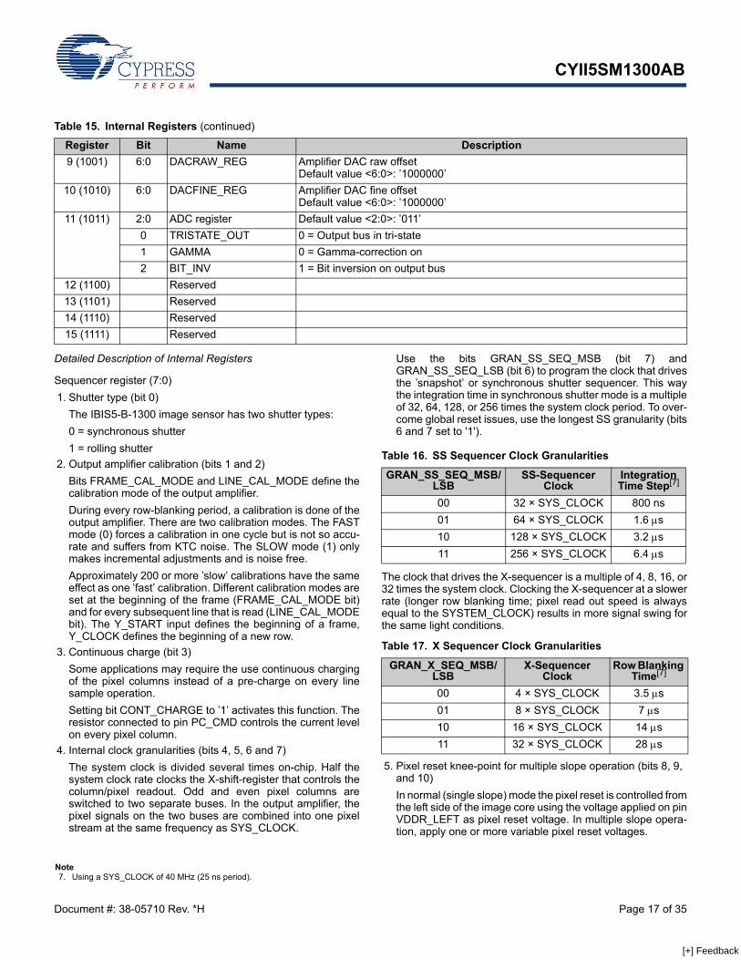
Use the bits GRAN_SS_SEQ_MSB (bit 7) andGRAN_SS_SEQ_LSB (bit 6) to program the clock that drivesthe ’snapshot’ or synchronous shutter sequencer. This waythe integration time in synchronous shutter mode is a multipleof 32, 64, 128, or 256 times the system clock period. To over-come global reset issues, use the longest SS granularity (bits6 and 7 set to '1').
.
The clock that drives the X-sequencer is a multiple of 4, 8, 16, or32 times the system clock. Clocking the X-sequencer at a slowerrate (longer row blanking time; pixel read out speed is alwaysequal to the SYSTEM_CLOCK) results in more signal swing forthe same light conditions.
5. Pixel reset knee-point for multiple slope operation (bits 8, 9, and 10)In normal (single slope) mode the pixel reset is controlled fromthe left side of the image core using the voltage applied on pinVDDR_LEFT as pixel reset voltage. In multiple slope opera-tion, apply one or more variable pixel reset voltages.
9 (1001) 6:0 DACRAW_REG Amplifier DAC raw offsetDefault value <6:0>: ’1000000’
10 (1010) 6:0 DACFINE_REG Amplifier DAC fine offsetDefault value <6:0>: ’1000000’
11 (1011) 2:0 ADC register Default value <2:0>: ’011’0 TRISTATE_OUT 0 = Output bus in tri-state1 GAMMA 0 = Gamma-correction on2 BIT_INV 1 = Bit inversion on output bus
12 (1100) Reserved13 (1101) Reserved14 (1110) Reserved15 (1111) Reserved
Table 15. Internal Registers (continued)
Register Bit Name Description
Table 16. SS Sequencer Clock Granularities
GRAN_SS_SEQ_MSB/LSB
SS-Sequencer Clock
Integration Time Step[7]
00 32 × SYS_CLOCK 800 ns01 64 × SYS_CLOCK 1.6 μs10 128 × SYS_CLOCK 3.2 μs11 256 × SYS_CLOCK 6.4 μs
Table 17. X Sequencer Clock Granularities
GRAN_X_SEQ_MSB/LSB
X-Sequencer Clock
Row Blanking Time[7]
00 4 × SYS_CLOCK 3.5 μs01 8 × SYS_CLOCK 7 μs10 16 × SYS_CLOCK 14 μs11 32 × SYS_CLOCK 28 μs
Note7. Using a SYS_CLOCK of 40 MHz (25 ns period).
[+] Feedback
CYII5SM1300AB
Document #: 38-05710 Rev. *H Page 18 of 35
Bits KNEE_POINT_MSB and KNEE_POINT_LSB select theon chip-generated pixel reset voltage.Bit KNEE_POINT_ENABLE set to ’1’ switches control to theright side of the image core so the pixel reset voltage(VDDR_RIGHT), selected by bits KNEE_POINT_MSB/LSB,is used.Use bit KNEE_POINT_ENABLE only for multiple slope oper-ation in synchronous shutter mode. In rolling shutter mode,use only the bits KNEE_POINT_MSB/LSB to select the sec-ond knee-point in dual slope operation. The actual knee-pointdepends on VDDH, VDDR_LEFT and VDDC applied to thesensor.
6. External Pixel Reset Voltage for Multiple Slope (bit 11)Setting bit VDDR_RIGHT_EXT to ’1’ disables the circuit thatgenerates the variable pixel reset voltage and uses the volt-age externally applied to pin VDDR_RIGHT as the dou-ble/multiple slope reset voltage.Setting bit VDDR_RIGHT_EXT to ’0’ allows you to monitor thevariable pixel reset voltage (used for multiple slope operation)on pin VDDR_RIGHT.
NROF_PIXELS Register (11:0)After the internal x_sync is generated (start of the pixel readoutof a particular row), the PIXEL_VALID signal goes high. ThePIXEL_VALID signal goes low when the pixel counter reachesthe value loaded in the NROF_PIXEL register. Due to the factthat two pixels are read at the same clock cycle, you must dividethis number by 2 (NROF_PIXELS = (width of ROI / 2) – 1).
ROF_LINES Register (11:0)After the internal yl_sync is generated (start of the frame readoutwith Y_START), the line counter increases with each Y_CLOCKpulse until it reaches the value loaded in the NROF_LINESregister and generates a LAST_LINE pulse. It must be noted that
the value loaded in the register must be (Number of linesrequired - 1).
INT_TIME Register (11:0)Use the INT_TIME register to set the integration time of theelectronic shutter. The interpretation of the INT_TIME dependson the chosen shutter type (rolling or synchronous).
Global shutterAfter the SS_START pulse is applied an internal countercounts the number of SS granulated clock cycles until itreaches the value loaded in the INT_TIME register and gen-erates a TIME_OUT pulse. Use this TIME_OUT pulse to gen-erate the SS_STOP pulse to stop the integration. When theINT_TIME register is used, the maximum integration time is:TINT_MAX = 212 × 256 (maximum granularity) × (40 MHZ)– 1 = 26.2 ms.You can increase this maximum time if you use an externalcounter to trigger SS_STOP. Ten is the minimal value that youcan load into the INT_TIME register (see also Internal clockgranularities (bits 4, 5, 6 and 7) on page 17).
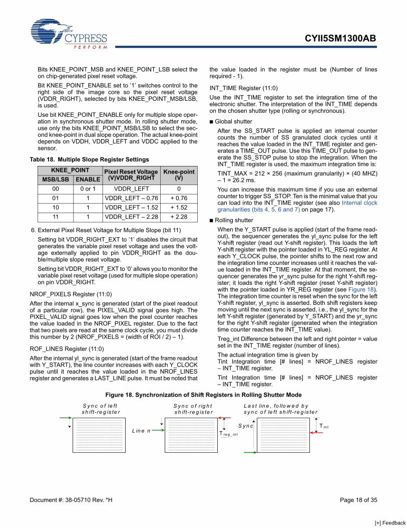
Rolling shutterWhen the Y_START pulse is applied (start of the frame read-out), the sequencer generates the yl_sync pulse for the leftY-shift register (read out Y-shift register). This loads the leftY-shift register with the pointer loaded in YL_REG register. Ateach Y_CLOCK pulse, the pointer shifts to the next row andthe integration time counter increases until it reaches the val-ue loaded in the INT_TIME register. At that moment, the se-quencer generates the yr_sync pulse for the right Y-shift reg-ister; it loads the right Y-shift register (reset Y-shift register)with the pointer loaded in YR_REG register (see Figure 18).The integration time counter is reset when the sync for the leftY-shift register, yl_sync is asserted. Both shift registers keepmoving until the next sync is asserted, i.e., the yl_sync for theleft Y-shift register (generated by Y_START) and the yr_syncfor the right Y-shift register (generated when the integrationtime counter reaches the INT_TIME value).Treg_int Difference between the left and right pointer = valueset in the INT_TIME register (number of lines).The actual integration time is given by Tint Integration time [# lines] = NROF_LINES register– INT_TIME register.Tint Integration time [# lines] = NROF_LINES register– INT_TIME register.
Figure 18. Synchronization of Shift Registers in Rolling Shutter Mode
Table 18. Multiple Slope Register Settings
KNEE_POINT Pixel Reset Voltage (V)VDDR_RIGHT
Knee-point (V)MSB/LSB ENABLE
00 0 or 1 VDDR_LEFT 001 1 VDDR_LEFT – 0.76 + 0.7610 1 VDDR_LEFT – 1.52 + 1.5211 1 VDDR_LEFT – 2.28 + 2.28
S y n c o f le f t s h if t - re g is te r
S y n c o f r ig h t s h if t - re g is te r
L in e n T re g _ in t
L a s t lin e , fo llo w e d b y s y n c o f le f t s h if t- re g is te r
T in tS y n c
[+] Feedback
CYII5SM1300AB
Document #: 38-05710 Rev. *H Page 19 of 35
X_REG Register (10:0)The X_REG register determines the start position of the windowin the X-direction. In this direction, there are 640 possible startingpositions (two pixels are addressed at the same time in one clockcycle). If sub sampling is enabled, only the even pixels are setas starting position (for instance: 0, 2, 4, 6, 8… 638).
YL_REG (10:0) and YR_REG (10:0)The YL_REG and YR_REG registers determine the start positionof the window in the Y-direction. In this direction, there are 1024possible starting positions. In rolling shutter mode the YL_REGregister sets the start position of the read (left) pointer and theYR_REG sets the start position of the reset (right) pointer. Forboth shutter types YL_REG is always equal to YR_REG.
Image Core Register (7:0)Bits 1:0 of the IMAGE_CORE register define the test mode of theimage core. Setting 00 is the default and normal operation mode.In case the bit is set to ‘1’, the odd (bit 1) or even (bit 0) columnsare tight to the reset level. If the internal ADC is used, bits 0 and1 are used to create test pattern to test the sample moment ofthe ADC. If the ADC sample moment is not chosen correctly, thecreated test pattern is not black-white-black-etc. (IMAGE_COREregister set at 1 or 2) or black-black-white-white-black-black(IMAGE_CORE register set at 9) but grey shadings if the sensoris saturated. Bits 7:2 of the IMAGE_CORE register define the sub-samplingmode in the X-direction (bits 4:2) and in the Y-direction (bits 7:5).The sub-sampling modes and corresponding bit setting aregiven in Table 11 and Table 12 on page 11.
Amplifier Register (6:0)1. GAIN (bits 3:0)
The gain bits determine the gain setting of the output amplifi-er. They are only effective if UNITY = 0. The gains and corre-sponding bit setting are given in Table 13 on page 12.
2. UNITY (bit 4)In case UNITY = 1, the gain setting of GAIN is bypassed andthe gain amplifier is put in unity feedback.
3. DUAL_OUT (bit 5)If DUAL_OUT = 1, the two output amplifiers are active. IfDUAL_OUT = 0, the signals from the two buses are multi-plexed to output PXL_OUT1 which connects to ADC_IN. Thegain amplifier and output driver of the second path are put instandby.
4. STANDBYIf STANDBY = 0, the complete output amplifier is put in stand-by. For normal use, set STANDBY to ‘1’.
DAC_RAW Register (6:0) and DAC_FINE (6:0) RegisterThese registers determine the black reference level at the outputof the output amplifier. Bit setting 1111111 for the DAC_RAW
register gives the highest offset voltage. Bit setting 0000000 forthe DAC_RAW register gives the lowest offset voltage. Ideally, ifthe two output paths have no offset mismatch, the DAC_FINEregister is set to 1000000. Deviation from this value is used tocompensate the internal mismatch (see Output Amplifier onpage 12).
ADC Register (2:0)1. TRISTATE_OUT (bit 0)
In case TRISTATE = 0, the ADC_D<9:0> outputs are intri-state mode. TRISTATE = 1 for normal operation mode.
2. GAMMA (bit 1)If GAMMA is set to ‘1’, the ADC input to output conversion islinear; otherwise the conversion follows a 'gamma' law (morecontrast in dark parts of the window, lower contrast in thebright parts).
3. BIT_INV (bit 2)If BIT_INV = 1, 0000000000 is the conversion of the lowestpossible input voltage, otherwise the bits are inverted.
Data InterfacesTwo different data interfaces are implemented. They areselected using pins IF_MODE (pin 12) and SER_MODE (pin 6).
Parallel InterfaceThe parallel interface uses a 16-bit parallel input (P_DATA(15:0)) to upload new register values. Asserting P_WRITE loadsthe parallel data into the internal register of the IBIS5-B-1300where it is decoded (see Figure 19). P_DATA (15:12) addressbits REG_ADDR (3:0); P_DATA (11:0) data bits REG_DATA(11:0).
Serial 3-Wire InterfaceThe serial 3-wire interface (or serial-to-parallel Interface) uses aserial input to shift the data in the register buffer. When thecomplete data word is shifted into the register buffer the dataword is loaded into the internal register where it is decoded (seeFigure 19). S_DATA (15:12) address bits REG_ADDR (3:0);S_DATA (11:0) data bits REG_DATA (11:0). When S_EN isasserted the parallel data is loaded into the internal registers ofthe IBIS5-B-1300. The maximum tested frequency of S_DATA is2.5 MHz.)
Serial 2-Wire InterfaceThe serial 2-wire interface is not operational in the IBIS5-B-1300image sensor. Use the 3-wire SPI interface to load the sensorregisters.
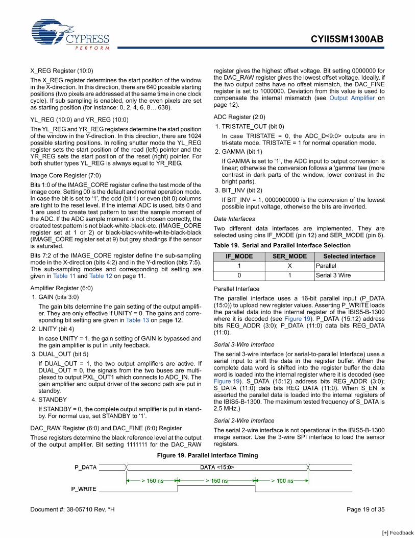
Figure 19. Parallel Interface Timing
Table 19. Serial and Parallel Interface Selection
IF_MODE SER_MODE Selected interface1 X Parallel0 1 Serial 3 Wire
[+] Feedback
CYII5SM1300AB
Document #: 38-05710 Rev. *H Page 20 of 35
Timing DiagramsFrame Rate The pixel rate for this sensor is high enough to support a framerate of greater than 100 Hz for a window size of 640 × 480 pixels(VGA format). Considering a row blanking time of 3.5 µs (asbaseline, see also Internal clock granularities (bits 4, 5, 6 and 7)on page 17), this requires a minimum pixel rate of nearly 40 MHz.The final bandwidth of the column amplifiers, output stage, andothers is determined by external bias resistors. With a nominalpixel rate of 40 MHz, a full frame rate of a little more than 27frames per second is obtained.The frame period of the IBIS5-B-1300 sensor depends on theshutter type.
Rolling Shutter=> Frame period = (Nr. Lines × (RBT + pixel period × Nr. Pixels))with: Nr. Lines Number of lines read out each frame (Y)Nr. Pixels Number of pixels read out each line (X)RBT Row blanking time = 3.5 µs (typical)Pixel period 1/40 MHz = 25 ns
Example Read out time of the full resolution at nominal speed(40-MHz pixel rate):Frame period = (1024 × (3.5 µs + 25 ns × 1280)) = 36.4 ms =27.5 fps
Global shutterFrame period = Tint + Tread out = Tint + (Nr. Lines × (RBT + pixel period × Nr. Pixels))with: Tint Integration (exposure) timeNr. Lines Number of lines read out each frame (Y)Nr. Pixels Number of pixels read out each line (X)RBT Row blanking time = 3.5 µs (typical)Pixel period 1/40 MHz = 25 ns
Example Read out time of the full resolution at nominal speed(40 MHz pixel rate) with an integration time of 1 ms:Frame period = 1 ms + (1024 × (3.5 µs + 25 ns × 1280)) =37.4 ms = 26.8 fps
Region-of-Interest (ROI) Read OutWindowing is easily achieved by uploading the starting point ofthe X- and Y-shift registers in the sensor registers using thevarious interfaces. This downloaded starting point initiates theshift register in the X- and Y-direction triggered by the Y_START(initiates the Y-shift register) and the Y_CLK (initiates the X-shiftregister) pulse. The minimum step size for the x-address is two(only even start addresses are chosen) and one for theY-address (every line is addressable). The frame rate increasesalmost linearly when fewer pixels are read out. Table 20 gives anoverview of the achievable frame rates (in rolling shutter mode)with various ROI dimensions.
Timing RequirementsThere are six control signals that operate the image sensor:
SS_START
SS_STOP
Y_CLOCK
Y_START
X_LOAD
SYS_CLOCKThe external system generates these control signals withfollowing time constraints to SYS_CLOCK (rising edge = activeedge):TSETUP >7.5 nsTHOLD > 7.5 nsIt is important that these signals are free of any glitches.
Table 20. Frame Rate vs. Resolution
Image Resolution
(X×Y)Frame Rate [frames/s]
Frame Readout Time
[ms]Comment
1280 × 1024 27 36 Full resolution.640 × 480 100 10 ROI read out.100 × 100 1657 0.6 ROI read out.
[+] Feedback
CYII5SM1300AB
Document #: 38-05710 Rev. *H Page 21 of 35
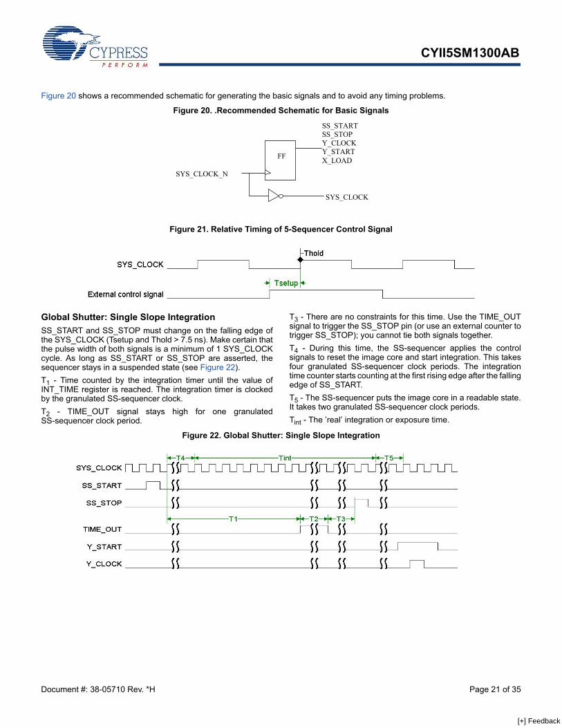
Figure 20 shows a recommended schematic for generating the basic signals and to avoid any timing problems.
Figure 20. .Recommended Schematic for Basic Signals
Figure 21. Relative Timing of 5-Sequencer Control Signal
Global Shutter: Single Slope IntegrationSS_START and SS_STOP must change on the falling edge ofthe SYS_CLOCK (Tsetup and Thold > 7.5 ns). Make certain thatthe pulse width of both signals is a minimum of 1 SYS_CLOCKcycle. As long as SS_START or SS_STOP are asserted, thesequencer stays in a suspended state (see Figure 22).T1 - Time counted by the integration timer until the value ofINT_TIME register is reached. The integration timer is clockedby the granulated SS-sequencer clock.T2 - TIME_OUT signal stays high for one granulatedSS-sequencer clock period.
T3 - There are no constraints for this time. Use the TIME_OUTsignal to trigger the SS_STOP pin (or use an external counter totrigger SS_STOP); you cannot tie both signals together. T4 - During this time, the SS-sequencer applies the controlsignals to reset the image core and start integration. This takesfour granulated SS-sequencer clock periods. The integrationtime counter starts counting at the first rising edge after the fallingedge of SS_START. T5 - The SS-sequencer puts the image core in a readable state.It takes two granulated SS-sequencer clock periods.Tint - The ’real’ integration or exposure time.
Figure 22. Global Shutter: Single Slope Integration
FF
SYS_CLOCK_N
SYS_CLOCK
SS_START SS_STOP Y_CLOCK Y_START X_LOAD
[+] Feedback
CYII5SM1300AB
Document #: 38-05710 Rev. *H Page 22 of 35
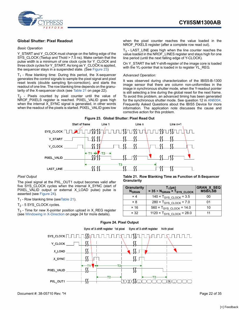
Global Shutter: Pixel Readout
Basic OperationY_START and Y_CLOCK must change on the falling edge of theSYS_CLOCK (Tsetup and Thold > 7.5 ns). Make certain that thepulse width is a minimum of one clock cycle for Y_CLOCK andthree clock cycles for Y_START. As long as Y_CLOCK is applied,the sequencer stays in a suspended state. (See Figure 23)T1 - Row blanking time: During this period, the X-sequencergenerates the control signals to sample the pixel signal and pixelreset levels (double sampling fpn-correction), and starts thereadout of one line. The row blanking time depends on the granu-larity of the X-sequencer clock (see Table 21 on page 22).T2 - Pixels counted by pixel counter until the value ofNROF_PIXELS register is reached. PIXEL_VALID goes highwhen the internal X_SYNC signal is generated, in other wordswhen the readout of the pixels is started. PIXEL_VALID goes low
when the pixel counter reaches the value loaded in theNROF_PIXELS register (after a complete row read out). T3 - LAST_LINE goes high when the line counter reaches thevalue loaded in the NROF_LINES register and stays high for oneline period (until the next falling edge of Y-CLOCK).On Y_START the left Y-shift-register of the image core is loadedwith the YL-pointer that is loaded in to register YL_REG.
Advanced Operation:It was observed during characterization of the IBIS5-B-1300image sensor that there are column non-uniformities in theimage in synchronous shutter mode, when the Y-readout pointeris still selecting a line during the global reset for the next frame.To avoid this problem, an advanced timing has been generatedfor the synchronous shutter mode. See question 12 in AN6004,Frequently Asked Questions about the IBIS5 Device for moreinformation. The application note discusses the cause andcorrective action for this problem.
Figure 23. Global Shutter: Pixel Read Out
Pixel OutputThe pixel signal at the PXL_OUT1 output becomes valid afterfive SYS_CLOCK cycles when the internal X_SYNC (start ofPIXEL_VALID output or external X_LOAD pulse) pulse isasserted (see Figure 24).T1 - Row blanking time (seeTable 21).T2 - 5 SYS_CLOCK cycles.T3 - Time for new X-pointer position upload in X_REG register(see Windowing in X-Direction on page 24 for more details).
Table 21. Row Blanking Time as Function of X-Sequencer Granularity
Figure 24. Pixel Output
GranularityNGRAN
T1(µs)= 35 × NGRAN × TSYS_CLOCK
GRAN_X_SEQMSB/LSB
× 4 140 × TSYS_CLOCK = 3.5 00× 8 280 × TSYS_CLOCK = 7.0 01
× 16 560 × TSYS_CLOCK = 14.0 10× 32 1120 × TSYS_CLOCK = 28.0 11
[+] Feedback
CYII5SM1300AB
Document #: 38-05710 Rev. *H Page 23 of 35
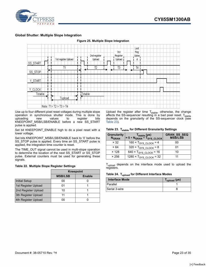
Global Shutter: Multiple Slope IntegrationFigure 25. Multiple Slope Integration
Use up to four different pixel reset voltages during multiple slopeoperation in synchronous shutter mode. This is done byuploading new values to register bitsKNEEPOINT_MSB/LSB/ENABLE before a new SS_STARTpulse is applied.Set bit KNEEPOINT_ENABLE high to do a pixel reset with alower voltage.Set bits KNEEPOINT_MSB/LSB/ENABLE back to ‘0’ before theSS_STOP pulse is applied. Every time an SS_START pulse isapplied, the integration time counter is reset.The TIME_OUT signal cannot be used in multi-slope operationto determine the location of the next SS_START or SS_STOPpulse. External counters must be used for generating thesesignals.
Upload the register after time Tstable, otherwise, the changeaffects the SS-sequencer resulting in a bad pixel reset. Tstabledepends on the granularity of the SS-sequencer clock (seeTable 23).
Tupload depends on the interface mode used to upload theregisters.Table 22. Multiple Slope Register Settings
KneepointMSB/LSB Enable
Initial Setup 00 01st Register Upload 01 12nd Register Upload 10 13th Register Upload 11 14th Register Upload 00 0
Table 23. Tstable for Different Granularity Settings
GranularityNGRAN
Tstable (µs) = 5 × NGRAN × TSYS_CLOCK
GRAN_SS_SEQMSB/LSB
× 32 160 × TSYS_CLOCK = 4 00× 64 320 × TSYS_CLOCK = 8 01× 128 640 × TSYS_CLOCK = 16 10× 256 1280 × TSYS_CLOCK = 32 11
Table 24. Tupload for Different Interface Modes
Interface Mode Tupload (µs)Parallel 1Serial 3-wire 8
[+] Feedback
CYII5SM1300AB
Document #: 38-05710 Rev. *H Page 24 of 35
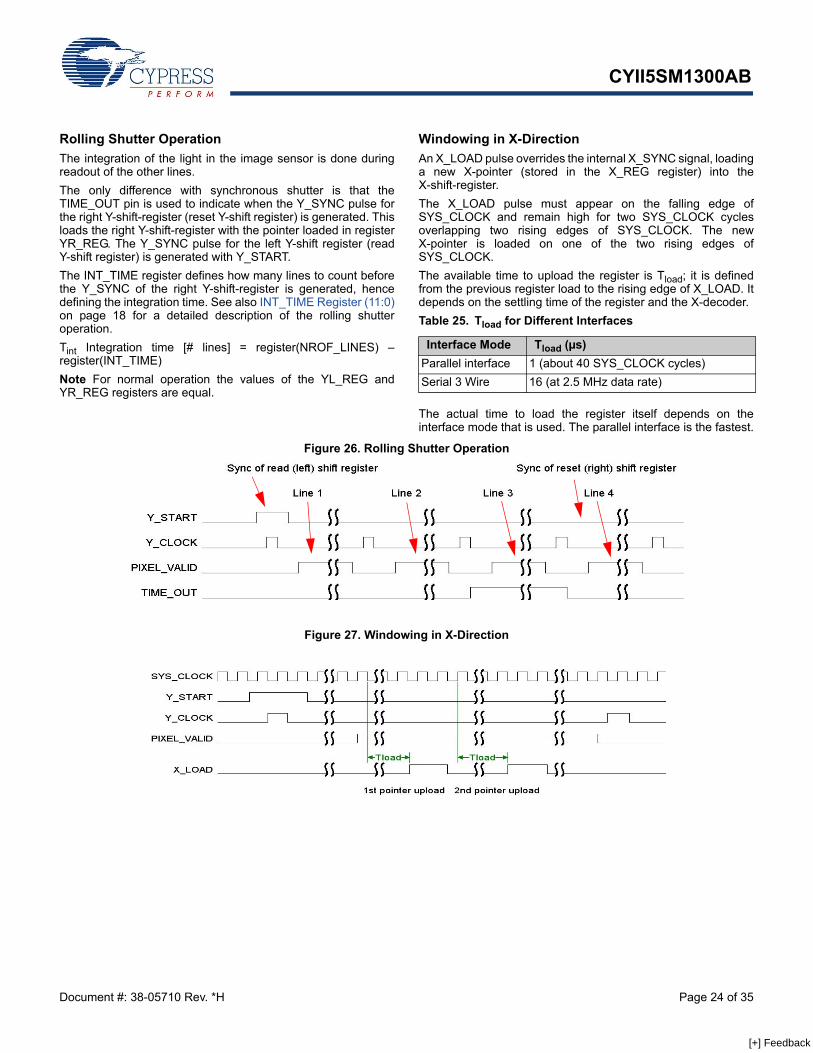
Rolling Shutter OperationThe integration of the light in the image sensor is done duringreadout of the other lines.The only difference with synchronous shutter is that theTIME_OUT pin is used to indicate when the Y_SYNC pulse forthe right Y-shift-register (reset Y-shift register) is generated. Thisloads the right Y-shift-register with the pointer loaded in registerYR_REG. The Y_SYNC pulse for the left Y-shift register (readY-shift register) is generated with Y_START.The INT_TIME register defines how many lines to count beforethe Y_SYNC of the right Y-shift-register is generated, hencedefining the integration time. See also INT_TIME Register (11:0)on page 18 for a detailed description of the rolling shutteroperation.Tint Integration time [# lines] = register(NROF_LINES) –register(INT_TIME)Note For normal operation the values of the YL_REG andYR_REG registers are equal.
Windowing in X-DirectionAn X_LOAD pulse overrides the internal X_SYNC signal, loadinga new X-pointer (stored in the X_REG register) into theX-shift-register.The X_LOAD pulse must appear on the falling edge ofSYS_CLOCK and remain high for two SYS_CLOCK cyclesoverlapping two rising edges of SYS_CLOCK. The newX-pointer is loaded on one of the two rising edges ofSYS_CLOCK.The available time to upload the register is Tload; it is definedfrom the previous register load to the rising edge of X_LOAD. Itdepends on the settling time of the register and the X-decoder.Table 25. Tload for Different Interfaces
The actual time to load the register itself depends on theinterface mode that is used. The parallel interface is the fastest.
Figure 26. Rolling Shutter Operation
Figure 27. Windowing in X-Direction
Interface Mode Tload (µs)Parallel interface 1 (about 40 SYS_CLOCK cycles)Serial 3 Wire 16 (at 2.5 MHz data rate)
[+] Feedback
CYII5SM1300AB
Document #: 38-05710 Rev. *H Page 25 of 35
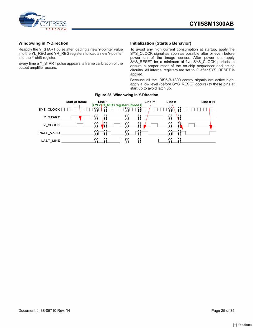
Windowing in Y-DirectionReapply the Y_START pulse after loading a new Y-pointer valueinto the YL_REG and YR_REG registers to load a new Y-pointerinto the Y-shift-register.Every time a Y_START pulse appears, a frame calibration of theoutput amplifier occurs.
Initialization (Startup Behavior)To avoid any high current consumption at startup, apply theSYS_CLOCK signal as soon as possible after or even beforepower on of the image sensor. After power on, applySYS_RESET for a minimum of five SYS_CLOCK periods toensure a proper reset of the on-chip sequencer and timingcircuitry. All internal registers are set to ‘0’ after SYS_RESET isapplied. Because all the IBIS5-B-1300 control signals are active high,apply a low level (before SYS_RESET occurs) to these pins atstart up to avoid latch up.
Figure 28. Windowing in Y-Direction
[+] Feedback
CYII5SM1300AB
Document #: 38-05710 Rev. *H Page 26 of 35
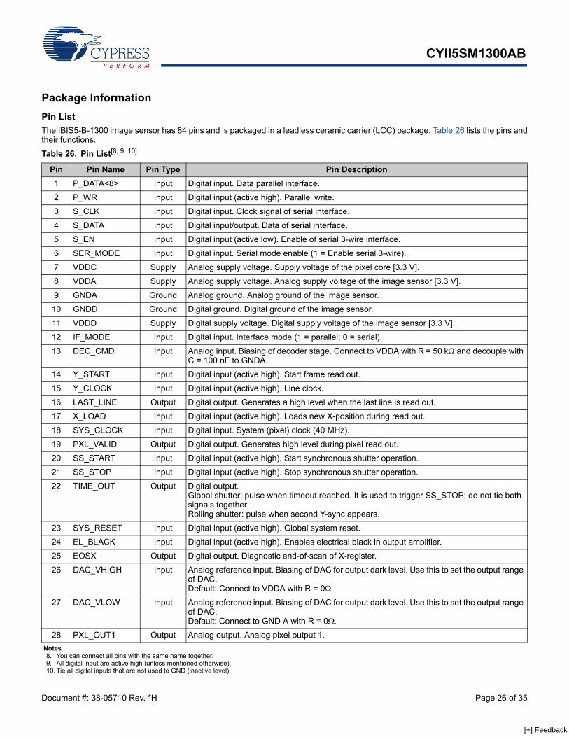
Package InformationPin ListThe IBIS5-B-1300 image sensor has 84 pins and is packaged in a leadless ceramic carrier (LCC) package. Table 26 lists the pins andtheir functions.
Table 26. Pin List[8, 9, 10]
Pin Pin Name Pin Type Pin Description1 P_DATA<8> Input Digital input. Data parallel interface.
2 P_WR Input Digital input (active high). Parallel write.
3 S_CLK Input Digital input. Clock signal of serial interface.
4 S_DATA Input Digital input/output. Data of serial interface.
5 S_EN Input Digital input (active low). Enable of serial 3-wire interface.
6 SER_MODE Input Digital input. Serial mode enable (1 = Enable serial 3-wire).
7 VDDC Supply Analog supply voltage. Supply voltage of the pixel core [3.3 V].
8 VDDA Supply Analog supply voltage. Analog supply voltage of the image sensor [3.3 V].
9 GNDA Ground Analog ground. Analog ground of the image sensor.
10 GNDD Ground Digital ground. Digital ground of the image sensor.
11 VDDD Supply Digital supply voltage. Digital supply voltage of the image sensor [3.3 V].
12 IF_MODE Input Digital input. Interface mode (1 = parallel; 0 = serial).
13 DEC_CMD Input Analog input. Biasing of decoder stage. Connect to VDDA with R = 50 kΩ and decouple with C = 100 nF to GNDA.
14 Y_START Input Digital input (active high). Start frame read out.
15 Y_CLOCK Input Digital input (active high). Line clock.
16 LAST_LINE Output Digital output. Generates a high level when the last line is read out.
17 X_LOAD Input Digital input (active high). Loads new X-position during read out.
18 SYS_CLOCK Input Digital input. System (pixel) clock (40 MHz).
19 PXL_VALID Output Digital output. Generates high level during pixel read out.
20 SS_START Input Digital input (active high). Start synchronous shutter operation.
21 SS_STOP Input Digital input (active high). Stop synchronous shutter operation.
22 TIME_OUT Output Digital output. Global shutter: pulse when timeout reached. It is used to trigger SS_STOP; do not tie both signals together.Rolling shutter: pulse when second Y-sync appears.
23 SYS_RESET Input Digital input (active high). Global system reset.
24 EL_BLACK Input Digital input (active high). Enables electrical black in output amplifier.
25 EOSX Output Digital output. Diagnostic end-of-scan of X-register.
26 DAC_VHIGH Input Analog reference input. Biasing of DAC for output dark level. Use this to set the output range of DAC.Default: Connect to VDDA with R = 0Ω.
27 DAC_VLOW Input Analog reference input. Biasing of DAC for output dark level. Use this to set the output range of DAC. Default: Connect to GND A with R = 0Ω.
28 PXL_OUT1 Output Analog output. Analog pixel output 1. Notes8. You can connect all pins with the same name together.9. All digital input are active high (unless mentioned otherwise). 10. Tie all digital inputs that are not used to GND (inactive level).
[+] Feedback
CYII5SM1300AB
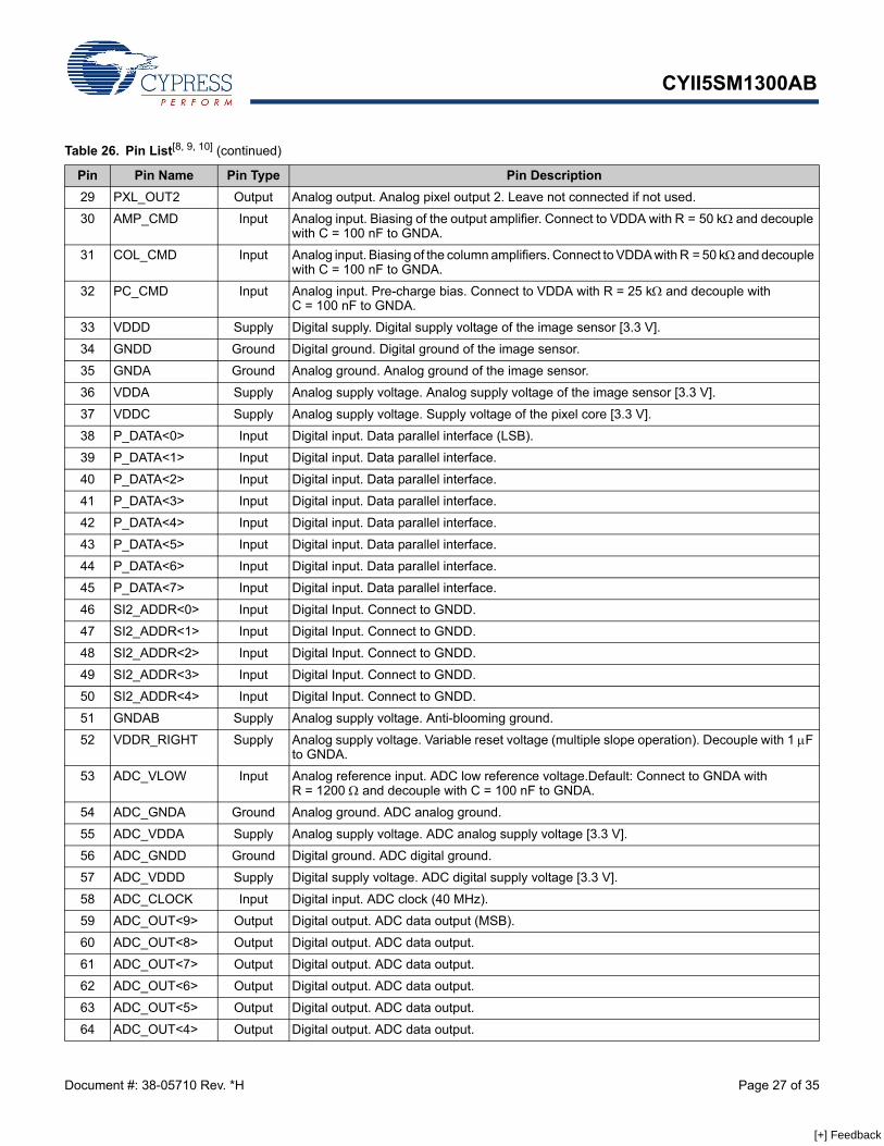
Document #: 38-05710 Rev. *H Page 27 of 35
29 PXL_OUT2 Output Analog output. Analog pixel output 2. Leave not connected if not used.
30 AMP_CMD Input Analog input. Biasing of the output amplifier. Connect to VDDA with R = 50 kΩ and decouple with C = 100 nF to GNDA.
31 COL_CMD Input Analog input. Biasing of the column amplifiers. Connect to VDDA with R = 50 kΩ and decouple with C = 100 nF to GNDA.
32 PC_CMD Input Analog input. Pre-charge bias. Connect to VDDA with R = 25 kΩ and decouple with C = 100 nF to GNDA.
33 VDDD Supply Digital supply. Digital supply voltage of the image sensor [3.3 V].
34 GNDD Ground Digital ground. Digital ground of the image sensor.
35 GNDA Ground Analog ground. Analog ground of the image sensor.
36 VDDA Supply Analog supply voltage. Analog supply voltage of the image sensor [3.3 V].
37 VDDC Supply Analog supply voltage. Supply voltage of the pixel core [3.3 V].
38 P_DATA<0> Input Digital input. Data parallel interface (LSB).
39 P_DATA<1> Input Digital input. Data parallel interface.
40 P_DATA<2> Input Digital input. Data parallel interface.
41 P_DATA<3> Input Digital input. Data parallel interface.
42 P_DATA<4> Input Digital input. Data parallel interface.
43 P_DATA<5> Input Digital input. Data parallel interface.
44 P_DATA<6> Input Digital input. Data parallel interface.
45 P_DATA<7> Input Digital input. Data parallel interface.
46 SI2_ADDR<0> Input Digital Input. Connect to GNDD.
47 SI2_ADDR<1> Input Digital Input. Connect to GNDD.
48 SI2_ADDR<2> Input Digital Input. Connect to GNDD.
49 SI2_ADDR<3> Input Digital Input. Connect to GNDD.
50 SI2_ADDR<4> Input Digital Input. Connect to GNDD.
51 GNDAB Supply Analog supply voltage. Anti-blooming ground.
52 VDDR_RIGHT Supply Analog supply voltage. Variable reset voltage (multiple slope operation). Decouple with 1 μF to GNDA.
53 ADC_VLOW Input Analog reference input. ADC low reference voltage.Default: Connect to GNDA with R = 1200 Ω and decouple with C = 100 nF to GNDA.
54 ADC_GNDA Ground Analog ground. ADC analog ground.
55 ADC_VDDA Supply Analog supply voltage. ADC analog supply voltage [3.3 V].
56 ADC_GNDD Ground Digital ground. ADC digital ground.
57 ADC_VDDD Supply Digital supply voltage. ADC digital supply voltage [3.3 V].
58 ADC_CLOCK Input Digital input. ADC clock (40 MHz).
59 ADC_OUT<9> Output Digital output. ADC data output (MSB).
60 ADC_OUT<8> Output Digital output. ADC data output.
61 ADC_OUT<7> Output Digital output. ADC data output.
62 ADC_OUT<6> Output Digital output. ADC data output.
63 ADC_OUT<5> Output Digital output. ADC data output.
64 ADC_OUT<4> Output Digital output. ADC data output.
Table 26. Pin List[8, 9, 10] (continued)
Pin Pin Name Pin Type Pin Description
[+] Feedback
CYII5SM1300AB
Document #: 38-05710 Rev. *H Page 28 of 35
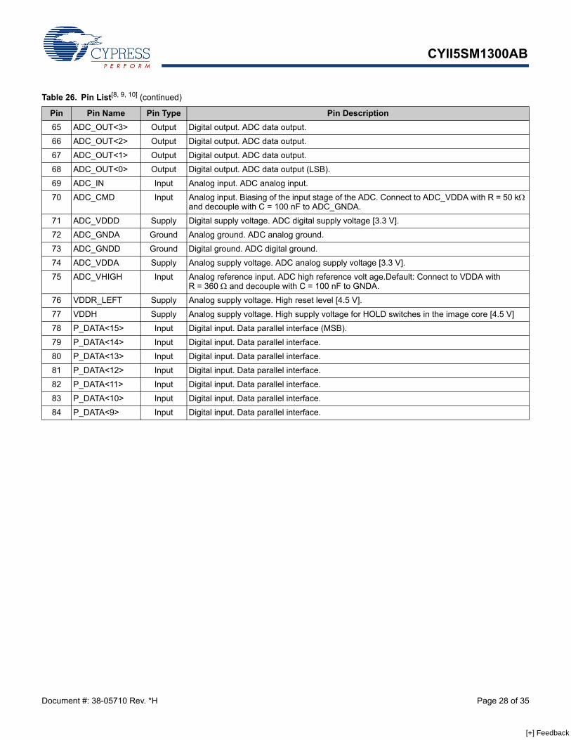
65 ADC_OUT<3> Output Digital output. ADC data output.
66 ADC_OUT<2> Output Digital output. ADC data output.
67 ADC_OUT<1> Output Digital output. ADC data output.
68 ADC_OUT<0> Output Digital output. ADC data output (LSB).
69 ADC_IN Input Analog input. ADC analog input.
70 ADC_CMD Input Analog input. Biasing of the input stage of the ADC. Connect to ADC_VDDA with R = 50 kΩ and decouple with C = 100 nF to ADC_GNDA.
71 ADC_VDDD Supply Digital supply voltage. ADC digital supply voltage [3.3 V].
72 ADC_GNDA Ground Analog ground. ADC analog ground.
73 ADC_GNDD Ground Digital ground. ADC digital ground.
74 ADC_VDDA Supply Analog supply voltage. ADC analog supply voltage [3.3 V].
75 ADC_VHIGH Input Analog reference input. ADC high reference volt age.Default: Connect to VDDA with R = 360 Ω and decouple with C = 100 nF to GNDA.
76 VDDR_LEFT Supply Analog supply voltage. High reset level [4.5 V].
77 VDDH Supply Analog supply voltage. High supply voltage for HOLD switches in the image core [4.5 V]
78 P_DATA<15> Input Digital input. Data parallel interface (MSB).
79 P_DATA<14> Input Digital input. Data parallel interface.
80 P_DATA<13> Input Digital input. Data parallel interface.
81 P_DATA<12> Input Digital input. Data parallel interface.
82 P_DATA<11> Input Digital input. Data parallel interface.
83 P_DATA<10> Input Digital input. Data parallel interface.
84 P_DATA<9> Input Digital input. Data parallel interface.
Table 26. Pin List[8, 9, 10] (continued)
Pin Pin Name Pin Type Pin Description
[+] Feedback
CYII5SM1300AB
Document #: 38-05710 Rev. *H Page 29 of 35
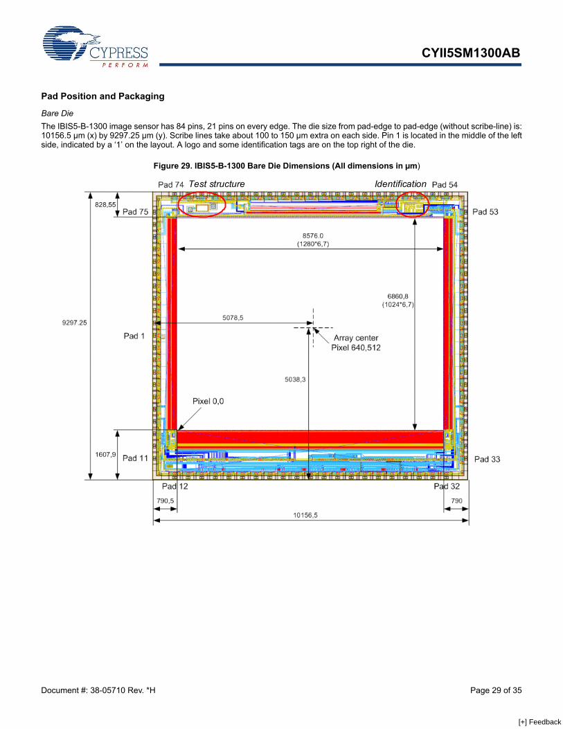
Pad Position and Packaging
Bare DieThe IBIS5-B-1300 image sensor has 84 pins, 21 pins on every edge. The die size from pad-edge to pad-edge (without scribe-line) is:10156.5 µm (x) by 9297.25 µm (y). Scribe lines take about 100 to 150 µm extra on each side. Pin 1 is located in the middle of the leftside, indicated by a ‘1’ on the layout. A logo and some identification tags are on the top right of the die.
Identification Test structure
Figure 29. IBIS5-B-1300 Bare Die Dimensions (All dimensions in µm)
[+] Feedback
CYII5SM1300AB
Document #: 38-05710 Rev. *H Page 30 of 35
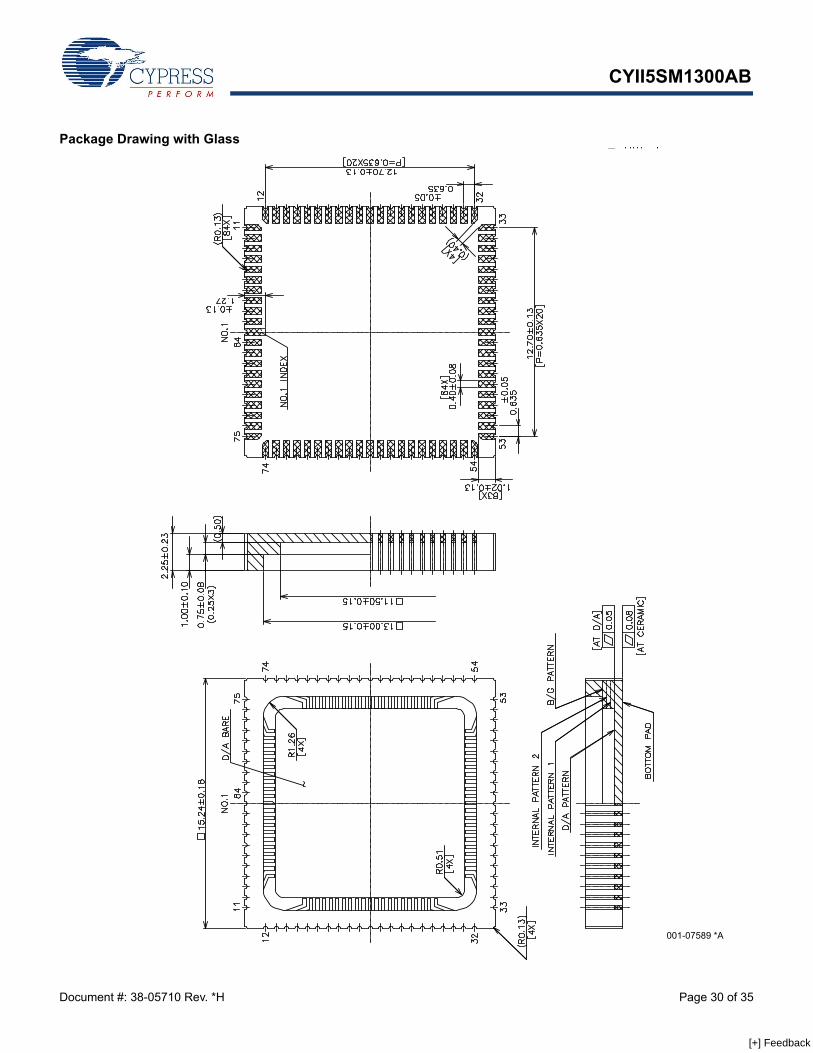
Package Drawing with Glass
001-07589 *A
[+] Feedback
CYII5SM1300AB
Document #: 38-05710 Rev. *H Page 31 of 35
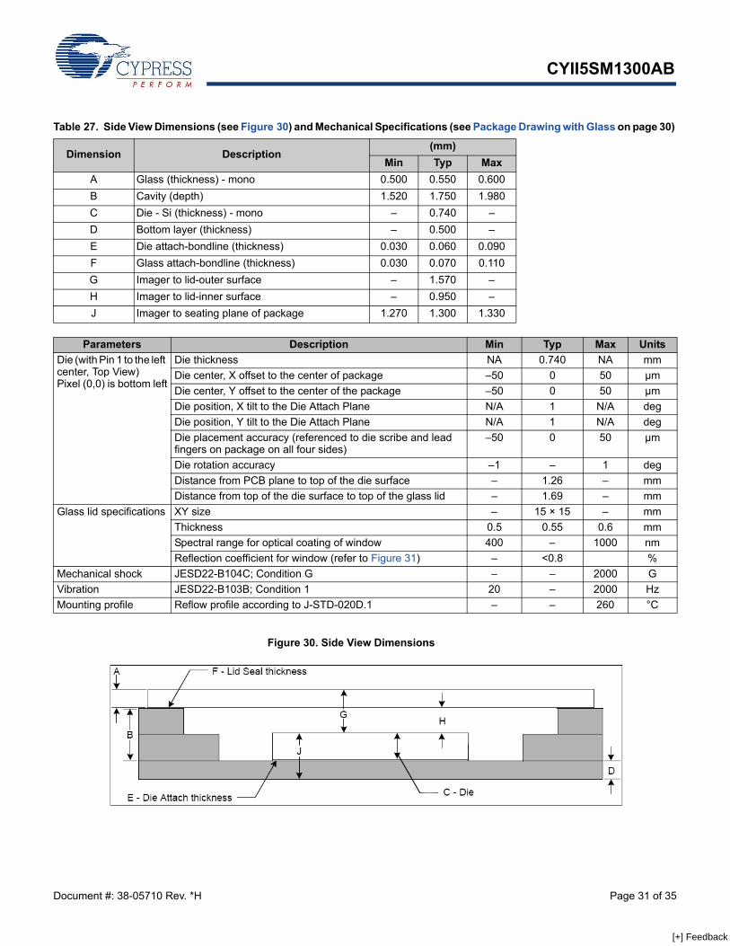
Table 27. Side View Dimensions (see Figure 30) and Mechanical Specifications (see Package Drawing with Glass on page 30)
Dimension Description(mm)
Min Typ MaxA Glass (thickness) - mono 0.500 0.550 0.600B Cavity (depth) 1.520 1.750 1.980C Die - Si (thickness) - mono – 0.740 –D Bottom layer (thickness) – 0.500 –E Die attach-bondline (thickness) 0.030 0.060 0.090F Glass attach-bondline (thickness) 0.030 0.070 0.110G Imager to lid-outer surface – 1.570 –H Imager to lid-inner surface – 0.950 –J Imager to seating plane of package 1.270 1.300 1.330
Parameters Description Min Typ Max UnitsDie (with Pin 1 to the left center, Top View)Pixel (0,0) is bottom left
Die thickness NA 0.740 NA mmDie center, X offset to the center of package –50 0 50 µmDie center, Y offset to the center of the package –50 0 50 µmDie position, X tilt to the Die Attach Plane N/A 1 N/A degDie position, Y tilt to the Die Attach Plane N/A 1 N/A degDie placement accuracy (referenced to die scribe and lead fingers on package on all four sides)
–50 0 50 µm
Die rotation accuracy –1 – 1 degDistance from PCB plane to top of the die surface – 1.26 – mmDistance from top of the die surface to top of the glass lid – 1.69 – mm
Glass lid specifications XY size – 15 × 15 – mmThickness 0.5 0.55 0.6 mmSpectral range for optical coating of window 400 – 1000 nmReflection coefficient for window (refer to Figure 31) – <0.8 %
Mechanical shock JESD22-B104C; Condition G – – 2000 GVibration JESD22-B103B; Condition 1 20 – 2000 HzMounting profile Reflow profile according to J-STD-020D.1 – – 260 °C
Figure 30. Side View Dimensions
[+] Feedback
CYII5SM1300AB
Document #: 38-05710 Rev. *H Page 32 of 35
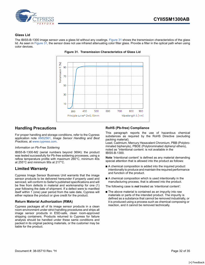
Glass LidThe IBIS5-B-1300 image sensor uses a glass lid without any coatings. Figure 31 shows the transmission characteristics of the glasslid. As seen in Figure 31, the sensor does not use infrared attenuating color filter glass. Provide a filter in the optical path when usingcolor devices.
Figure 31. Transmission Characteristics of Glass Lid
Handling PrecautionsFor proper handling and storage conditions, refer to the Cypressapplication note AN52561, Image Sensor Handling and BestPractices, at www.cypress.com.
Information on Pb-Free SolderingIBIS5-B-1300-M2 (serial numbers beyond 3694): the productwas tested successfully for Pb-free soldering processes, using areflow temperature profile with maximum 260°C, minimum 40sat 255°C and minimum 90s at 217°C.
Limited WarrantyCypress Image Sensor Business Unit warrants that the imagesensor products to be delivered hereunder if properly used andserviced, will conform to Seller's published specifications and willbe free from defects in material and workmanship for one (1)year following the date of shipment. If a defect were to manifestitself within 1 (one) year period from the sale date, Cypress willeither replace the product or give credit for the product.
Return Material Authorization (RMA)Cypress packages all of its image sensor products in a cleanroom environment under strict handling procedures and ships allimage sensor products in ESD-safe, clean room-approvedshipping containers. Products returned to Cypress for failureanalysis should be handled under these same conditions andpacked in its original packing materials, or the customer may beliable for the product.
RoHS (Pb-free) ComplianceThis paragraph reports the use of hazardous chemicalsubstances as required by the RoHS Directive (excludingpacking material). Lead, Cadmium, Mercury Hexavalent Chromium, PBB (Polybro-minated biphenyls), PBDE (Polybrominated diphenyl ethers), noted as “intentional content: is not available in the IBIS5-B-1300.Note ‘Intentional content’ is defined as any material demandingspecial attention that is allowed into the product as follows:
A chemical composition is added into the inquired product intentionally to produce and maintain the required performance and function of the product.
A chemical composition which is used intentionally in the manufacturing process, that is allowed into the product.
The following case is not treated as ‘intentional content’:
The above material is contained as an impurity into raw materials or parts of the intended product. The impurity is defined as a substance that cannot be removed industrially, or it is produced using a process such as chemical composing or reaction, and it cannot be removed technically.
[+] Feedback
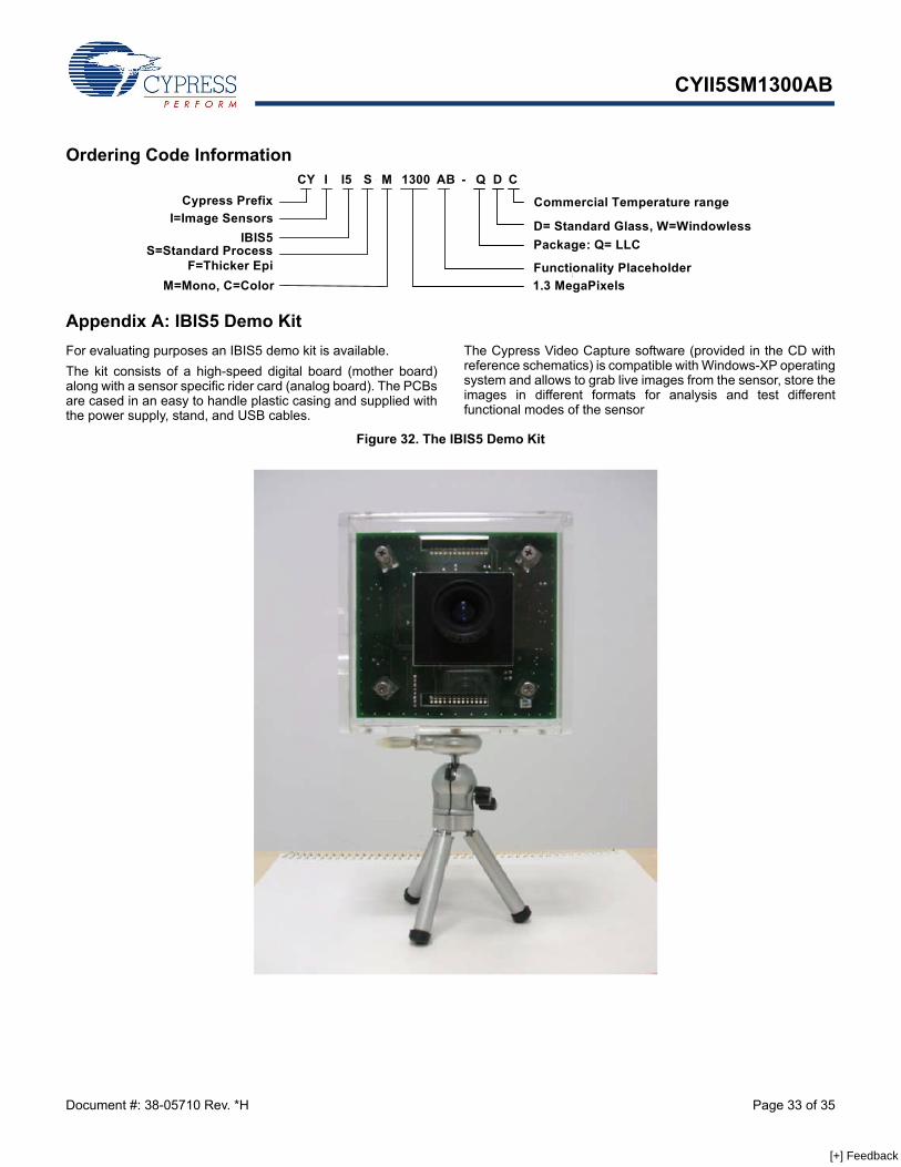
CYII5SM1300AB
Document #: 38-05710 Rev. *H Page 33 of 35
Ordering Code Information
Appendix A: IBIS5 Demo KitFor evaluating purposes an IBIS5 demo kit is available. The kit consists of a high-speed digital board (mother board)along with a sensor specific rider card (analog board). The PCBsare cased in an easy to handle plastic casing and supplied withthe power supply, stand, and USB cables.
The Cypress Video Capture software (provided in the CD withreference schematics) is compatible with Windows-XP operatingsystem and allows to grab live images from the sensor, store theimages in different formats for analysis and test differentfunctional modes of the sensor
Figure 32. The IBIS5 Demo Kit
I=Image SensorsCypress Prefix
IBIS5
M=Mono, C=Color
Package: Q= LLC
Commercial Temperature range
CY I I5 AB1300MS Q- D C
S=Standard ProcessF=Thicker Epi
1.3 MegaPixelsFunctionality Placeholder
D= Standard Glass, W=Windowless
[+] Feedback
CYII5SM1300AB
Document #: 38-05710 Rev. *H Page 34 of 35
Document History Page
Document Title: CYII5SM1300AB IBIS5 1.3 Megapixel CMOS Image SensorDocument Number: 38-05710
Rev. ECN No. Orig. of Change
Submission Date Description of Change
** 310213 FVK See ECN New Data Sheet*A 649064 FPW See ECN Ordering information update and new layout.
Implemented the new template. Moved figure captions to the top of the figures and moved notes to the bottom of the page per new template. Verified all cross-referencing. Moved the specifications towards the back. Corrected one variable on the Master pages. Spelled checked.
*B 1162847 FPW/ARI See ECN BGA package information removed. Implemented new template. Edited for template compliance.
*C 1417584 FPW See ECN Die placement drawing update*D 2765859 NVEA 09/18/09 Updated Ordering Information table*E 2786518 SHEA 10/14/09 Minor ECN to correct copyright year*F 2903130 NVEA 04/01/10 Removed reference to I2C, IBIS5-A. Updated Figure 23, Added dynamic
currents to Table 26. Updated Appendix A. Added handling and limited warranty statement.
*G 3056594 NVEA 10/12/2010 Removed MPN: CYII5FM1300AB-QWCReformatted and edited section “Specifications” on page 3. Edited“Color Filter Arrangement of Pixels” on page 6, “Spectral Response for IBIS5-B-Color” on page 6, “Overview of Bias Signals” on page 10. Added new section “Black Calibration” on page 14.Edited “Rolling Shutter Operation” on page 15, “Global Shutter Operation” on page 15 and “Transmission Characteristics of Glass Lid” on page 32.Added table “Side View Dimensions (see Figure 30) and Mechanical Specifications (see Package Drawing with Glass on page 30)” on page 31, “Glass Lid” on page 32, “Ordering Code Information” on page 33.
*H 3137684 NVEA 1/13/2011 Removed EVAL MPNs in Ordering Information. Edited the error in PLS value in Electro Optical Specifications.
[+] Feedback
Document #: 38-05710 Rev. *H Revised January 13, 2011 Page 35 of 35
All products and company names mentioned in this document may be the trademarks of their respective holders.
CYII5SM1300AB
© Cypress Semiconductor Corporation, 2005-2011. The information contained herein is subject to change without notice. Cypress Semiconductor Corporation assumes no responsibility for the use ofany circuitry other than circuitry embodied in a Cypress product. Nor does it convey or imply any license under patent or other rights. Cypress products are not warranted nor intended to be used formedical, life support, life saving, critical control or safety applications, unless pursuant to an express written agreement with Cypress. Furthermore, Cypress does not authorize its products for use ascritical components in life-support systems where a malfunction or failure may reasonably be expected to result in significant injury to the user. The inclusion of Cypress products in life-support systemsapplication implies that the manufacturer assumes all risk of such use and in doing so indemnifies Cypress against all charges.
Any Source Code (software and/or firmware) is owned by Cypress Semiconductor Corporation (Cypress) and is protected by and subject to worldwide patent protection (United States and foreign),United States copyright laws and international treaty provisions. Cypress hereby grants to licensee a personal, non-exclusive, non-transferable license to copy, use, modify, create derivative works of,and compile the Cypress Source Code and derivative works for the sole purpose of creating custom software and or firmware in support of licensee product to be used only in conjunction with a Cypressintegrated circuit as specified in the applicable agreement. Any reproduction, modification, translation, compilation, or representation of this Source Code except as specified above is prohibited withoutthe express written permission of Cypress.
Disclaimer: CYPRESS MAKES NO WARRANTY OF ANY KIND, EXPRESS OR IMPLIED, WITH REGARD TO THIS MATERIAL, INCLUDING, BUT NOT LIMITED TO, THE IMPLIED WARRANTIESOF MERCHANTABILITY AND FITNESS FOR A PARTICULAR PURPOSE. Cypress reserves the right to make changes without further notice to the materials described herein. Cypress does notassume any liability arising out of the application or use of any product or circuit described herein. Cypress does not authorize its products for use as critical components in life-support systems wherea malfunction or failure may reasonably be expected to result in significant injury to the user. The inclusion of Cypress’ product in a life-support systems application implies that the manufacturerassumes all risk of such use and in doing so indemnifies Cypress against all charges.
Use may be limited by and subject to the applicable Cypress software license agreement.
Sales, Solutions, and Legal InformationWorldwide Sales and Design SupportCypress offers standard and customized CMOS image sensors for consumer as well as industrial and professional applications.Consumer applications include solutions for fast growing high speed machine vision, motion monitoring, medical imaging, intelligenttraffic systems, security, and barcode applications. Cypress's customized CMOS image sensors are characterized by very high pixelcounts, large area, very high frame rates, large dynamic range, and high sensitivity.Cypress maintains a worldwide network of offices, solution centers, manufacturer's representatives, and distributors. For moreinformation on image sensors, contact [email protected].
[+] Feedback