
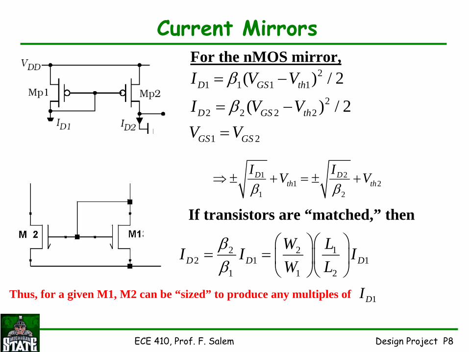
Current Mirrors - Michigan State University · Current Mirrors . 2 11 1 1 2 22 2 2 12 ()/2 ......
16
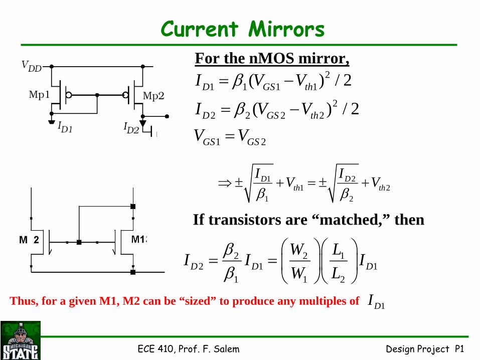
ECE 410, Prof. F. Salem Design Project P1 Current Mirrors . 2 1 1 1 1 2 2 2 2 2 1 2 ( ) /2 ( ) /2 D GS th D GS th GS GS I V V I V V V V β β = − = − = 1 2 1 2 1 2 D D th th I I V V β β ⇒± + =± + 2 2 1 2 1 1 1 1 2 D D D W L I I I W L β β ⎛ ⎞⎛ ⎞ = = ⎜ ⎟⎜ ⎟ ⎝ ⎠⎝ ⎠ For the nMOS mirror, If transistors are “matched,” then Thus, for a given M1, M2 can be “sized” to produce any multiples of 1 D I
-
Upload
truongdung -
Category
Documents
-
view
227 -
download
0
Transcript of Current Mirrors - Michigan State University · Current Mirrors . 2 11 1 1 2 22 2 2 12 ()/2 ......
ECE 410, Prof. F. Salem Design Project P1
Current Mirrors .
21 1 1 1
22 2 2 2
1 2
( ) / 2
( ) / 2D GS th
D GS th
GS GS
I V V
I V VV V
β
β
= −
= −=
1 21 2
1 2
D Dth th
I IV Vβ β
⇒ ± + = ± +
2 2 12 1 1
1 1 2D D D
W LI I IW L
ββ
⎛ ⎞⎛ ⎞= = ⎜ ⎟⎜ ⎟
⎝ ⎠⎝ ⎠
For the nMOS mirror,
If transistors are “matched,” then
Thus, for a given M1, M2 can be “sized” to produce any multiples of 1DI
ECE 410, Prof. F. Salem Design Project P2
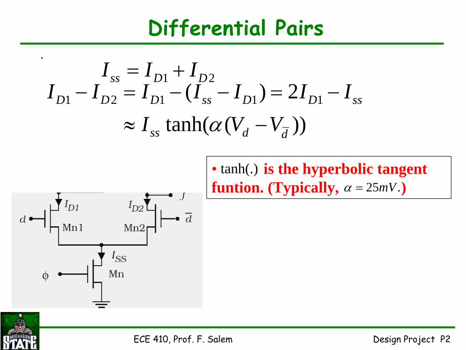
Differential Pairs .
1 2ss D DI I I= +1 2 1 1 1( ) 2
tanh( ( ))D D D ss D D ss
ss d d
I I I I I I II V Vα
− = − − = −≈ −
• is the hyperbolic tangent funtion. (Typically, )
tanh(.)25 .mVα =
ECE 410, Prof. F. Salem Design Project P3
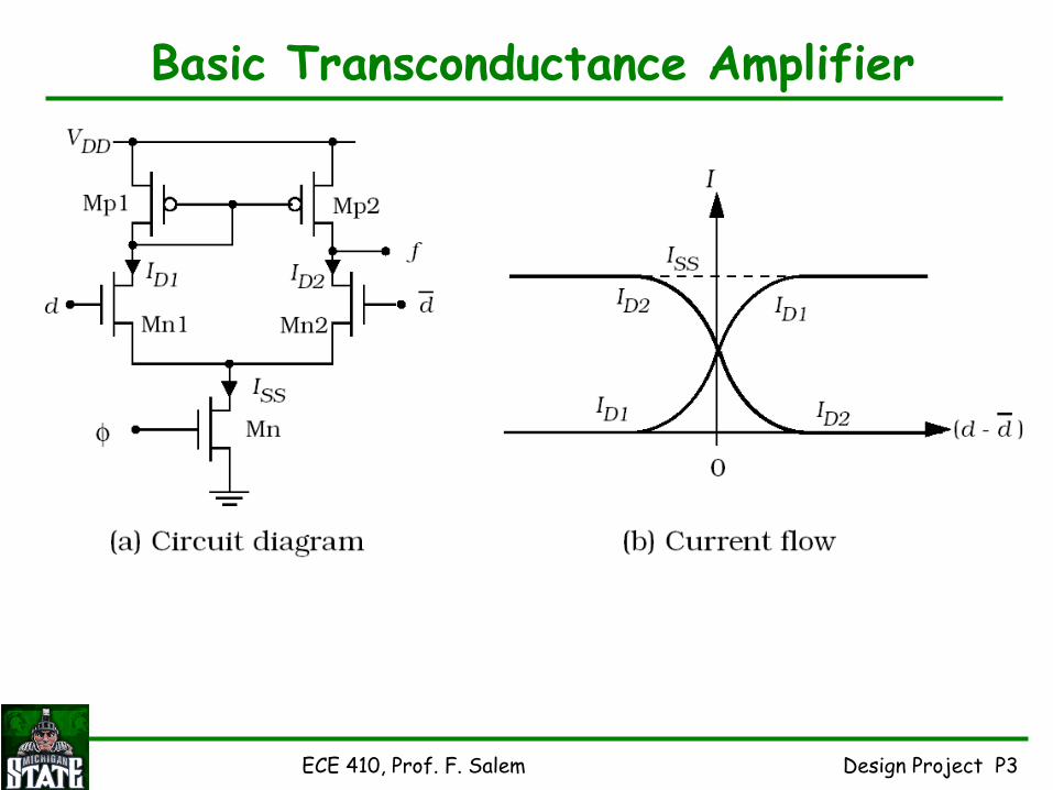
Basic Transconductance
Amplifier .
The chip design is comprised of three stages
•High Level (“system” specifications, block definitions)
•Component Level (Architectural/topology, simulations)
•Layout Level (Cadence LVS, DRC,..)
ECE 410, Prof. F. Salem Design Project P4
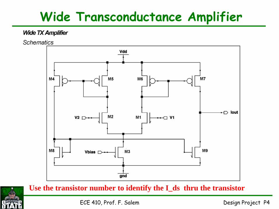
Wide Transconductance
Amplifier .
Use the transistor number to identify the I_ds thru the transistor
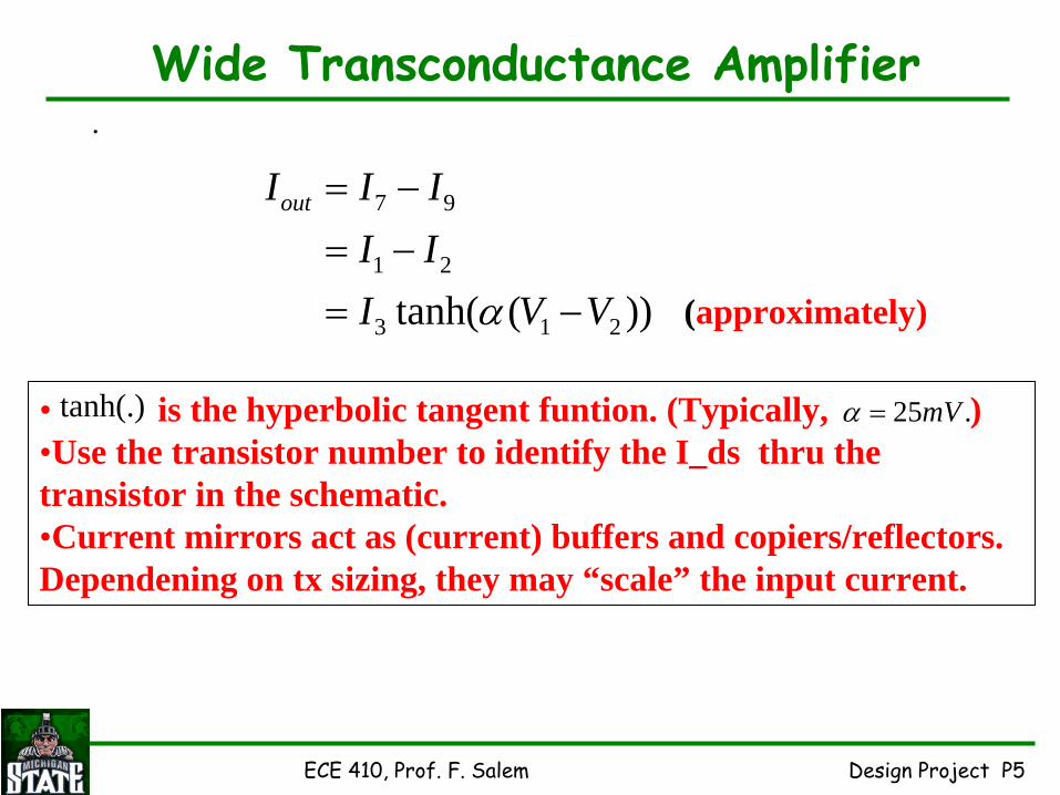
ECE 410, Prof. F. Salem Design Project P5
Wide Transconductance
Amplifier.
• is the hyperbolic tangent funtion. (Typically, )•Use the transistor number to identify the I_ds thru the transistor in the schematic.•Current mirrors act as (current) buffers and copiers/reflectors. Dependening on tx sizing, they may “scale” the input current.
7 9
1 2
3 1 2tanh( ( ))
outI I II II V Vα
= −
= −= − (approximately)
tanh(.) 25 .mVα =
ECE 410, Prof. F. Salem Design Project P6
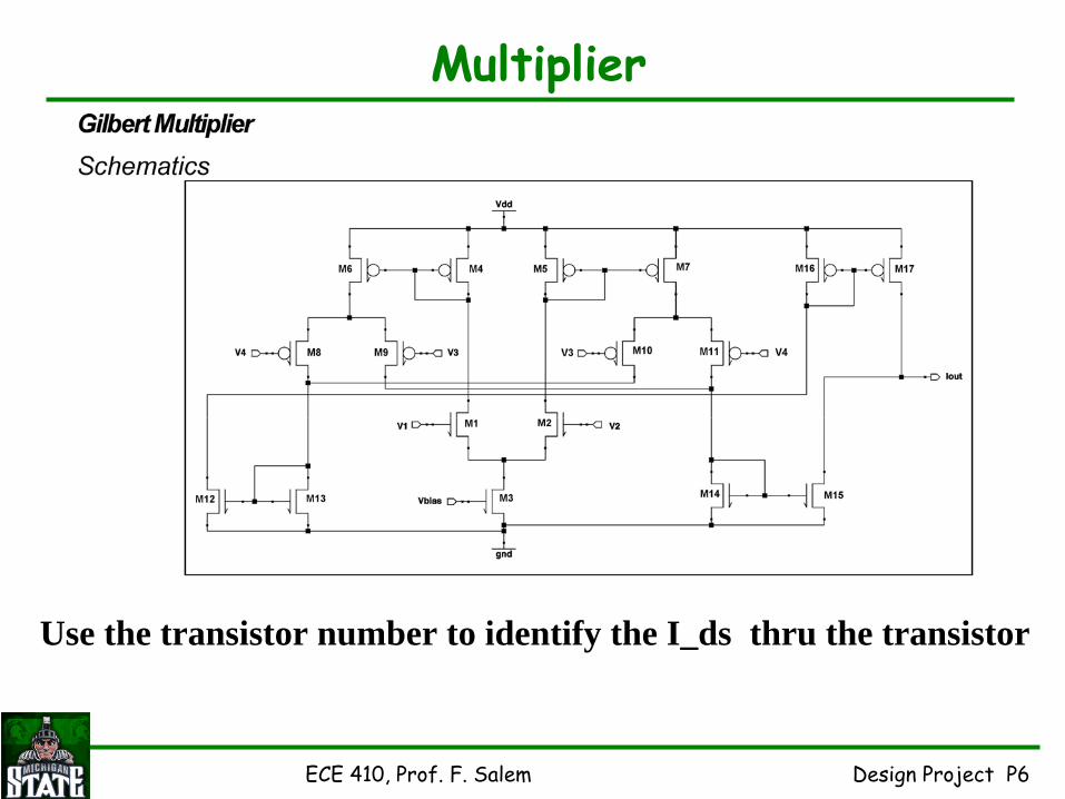
Multiplier .
Use the transistor number to identify the I_ds thru the transistor
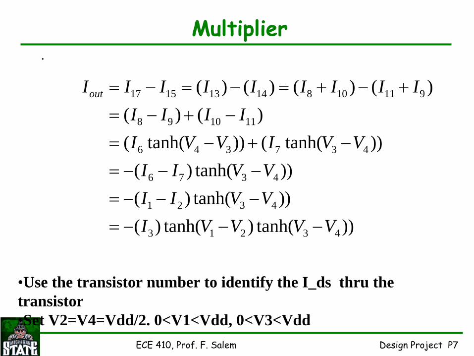
ECE 410, Prof. F. Salem Design Project P7
Multiplier .
17 15 13 14 8 10 11 9
8 9 10 11
6 4 3 7 3 4
6 7 3 4
1 2 3 4
3 1 2 3 4
( ) ( ) ( ) ( )( ) ( )( tanh( )) ( tanh( ))
( ) tanh( ))( ) tanh( ))( ) tanh( ) tanh( ))
outI I I I I I I I II I I II V V I V V
I I V VI I V VI V V V V
= − = − = + − += − + −
= − + −
= − − −
= − − −
= − − −
•Use the transistor number to identify the I_ds thru the transistor•Set V2=V4=Vdd/2. 0<V1<Vdd, 0<V3<Vdd
ECE 410, Prof. F. Salem Design Project P8
Current Mirrors .
21 1 1 1
22 2 2 2
1 2
( ) / 2
( ) / 2D GS th
D GS th
GS GS
I V V
I V VV V
β
β
= −
= −=
1 21 2
1 2
D Dth th
I IV Vβ β
⇒ ± + = ± +
2 2 12 1 1
1 1 2D D D
W LI I IW L
ββ
⎛ ⎞⎛ ⎞= = ⎜ ⎟⎜ ⎟
⎝ ⎠⎝ ⎠
For the nMOS mirror,
If transistors are “matched,” then
Thus, for a given M1, M2 can be “sized” to produce any multiples of 1DI
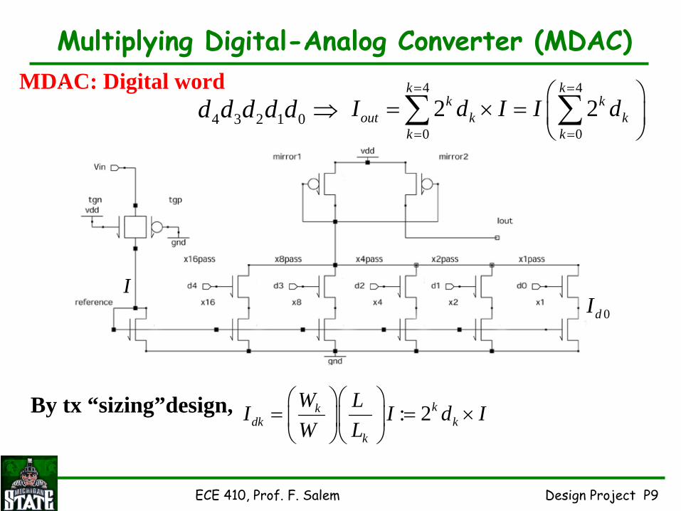
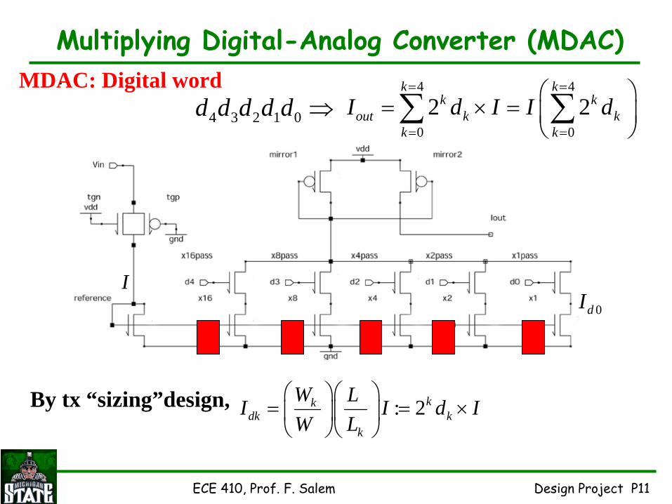
ECE 410, Prof. F. Salem Design Project P9
Multiplying Digital-Analog Converter (MDAC).
I0dI
: 2kkdk k
k
W LI I d IW L
⎛ ⎞⎛ ⎞= = ×⎜ ⎟⎜ ⎟⎝ ⎠⎝ ⎠
4 4
0 02 2
k kk k
out k kk k
I d I I d= =
= =
⎛ ⎞= × = ⎜ ⎟
⎝ ⎠∑ ∑
By tx “sizing”design,
4 3 2 1 0d d d d d ⇒MDAC: Digital word
ECE 410, Prof. F. Salem Design Project P10
Multiplying Digital-Analog Converter (MDAC).
4 4
10 02 2
k kk k
out k kk k
I d I I d= =
= =
⎛ ⎞= × = ⇒⎜ ⎟
⎝ ⎠∑ ∑
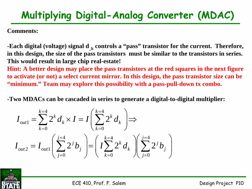
Comments:
-Each digital (voltage) signal d_k controls a “pass” transistor for the current. Therefore, in this design, the size of the pass transistors must be similar to the transistors in series. This would result in large chip real-estate! Hint: A better design may place the pass transistors at the red squares in the next figureto activate (or not) a select current mirror. In this design, the pass transistor size can be “minimum.” Team may explore this possibility with a pass-pull-down tx combo.
-Two MDACs can be cascaded in series to generate a digital-to-digital multiplier:
4 44
2 10 0 02 2 2
j jkj k j
out out j k jj k j
I I b I d b= ==
= = =
⎛ ⎞ ⎛ ⎞⎛ ⎞= =⎜ ⎟ ⎜ ⎟⎜ ⎟
⎝ ⎠⎝ ⎠ ⎝ ⎠∑ ∑ ∑
ECE 410, Prof. F. Salem Design Project P11
Multiplying Digital-Analog Converter (MDAC).
I0dI
: 2kkdk k
k
W LI I d IW L
⎛ ⎞⎛ ⎞= = ×⎜ ⎟⎜ ⎟⎝ ⎠⎝ ⎠
4 4
0 02 2
k kk k
out k kk k
I d I I d= =
= =
⎛ ⎞= × = ⎜ ⎟
⎝ ⎠∑ ∑
By tx “sizing”design,
4 3 2 1 0d d d d d ⇒MDAC: Digital word
ECE 410, Prof. F. Salem Design Project P12
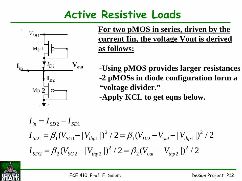
Active Resistive Loads .
2 12 2
1 1 1 1 1 1
2 22 2 2 2 2 2
( | |) / 2 ( | |) / 2
( | |) / 2 ( | |) / 2
in SD SD
SD SG thp DD out thp
SD SG thp out thp
I I I
I V V V V V
I V V V V
β β
β β
= −
= − = − −
= − = −
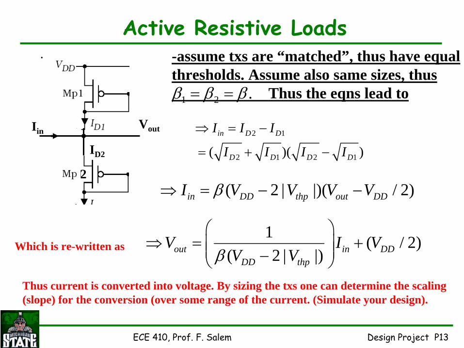
For two pMOS in series, driven by thecurrent Iin, the voltage Vout is derived as follows:
2
ID2
IinVout -Using pMOS provides larger resistances
-2 pMOSs in diode configuration form a “voltage divider.”-Apply KCL to get eqns below.
ECE 410, Prof. F. Salem Design Project P13
Active Resistive Loads .
( 2 | |)( / 2)in DD thp out DDI V V V Vβ⇒ = − −
2 1
2 1 2 1( )( )in D D
D D D D
I I I
I I I I
⇒ = −
= + −
-assume txs are “matched”, thus have equalthresholds. Assume also same sizes, thus
Thus the eqns lead to
Which is re-written as
2
ID2
IinVout
1 2 .β β β= =
1 ( / 2)( 2 | |)out in DD
DD thp
V I VV Vβ
⎛ ⎞⇒ = +⎜ ⎟⎜ ⎟−⎝ ⎠
Thus current is converted into voltage. By sizing the txs one can determine the scaling (slope) for the conversion (over some range of the current. (Simulate your design).
ECE 410, Prof. F. Salem Design Project P14
Active Resistive Loads .
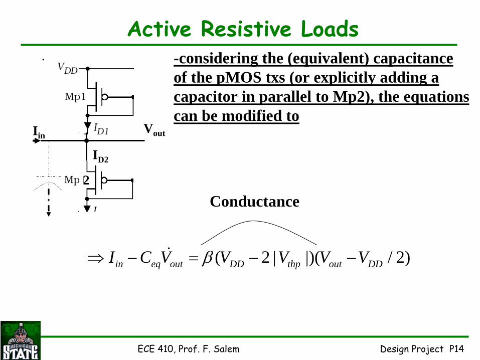
( 2 | |)( / 2)in eq out DD thp out DDI C V V V V Vβ⇒ − = − −
-considering the (equivalent) capacitance of the pMOS txs (or explicitly adding a capacitor in parallel to Mp2), the equations can be modified to
2
ID2
IinVout
Conductance

ECE 410, Prof. F. Salem Design Project P15
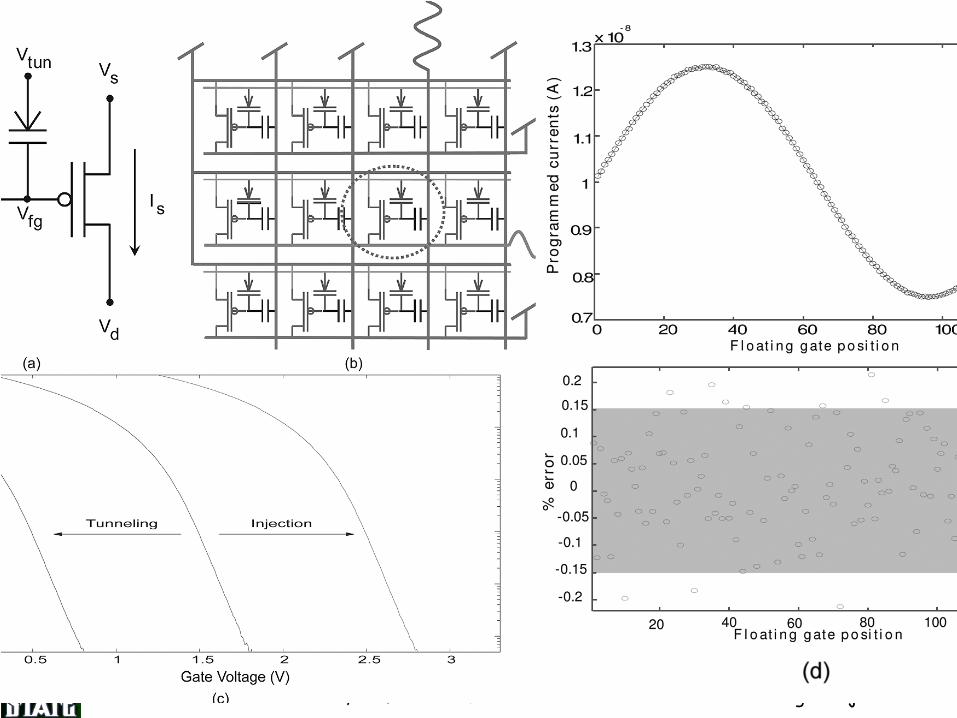
pMOS
floating gates -Use a pMOS
for a floating gate (FG). -Impossible to program nMOS
due to specifics of fab. control process techniques. Easier to program a pMOS.
-Use tunneling to remove electron from FG |Vtp| is increased. This is used for Global “erase.”
-Use hot-electron injection to place electrons on FG, thus reducing |Vtp|. This is used for selectively “programming”
each FG in an array.
ECE 410, Prof. F. Salem Design Project P16
Active Resistive Loads .
( 2 | |)( / 2)in eq out DD thp out DDI C V V V V Vβ⇒ − = − −
-considering the (equivalent) capacitance of the pMOS txs (or explicitly adding a capacitor in parallel to Mp2), the equations can be modified to
2
ID2
IinVout
Conductance