CSE 370 Sample Final Exam Questions · Sample Final Exam Questions 1) Logic Minimization CD AB ......
21
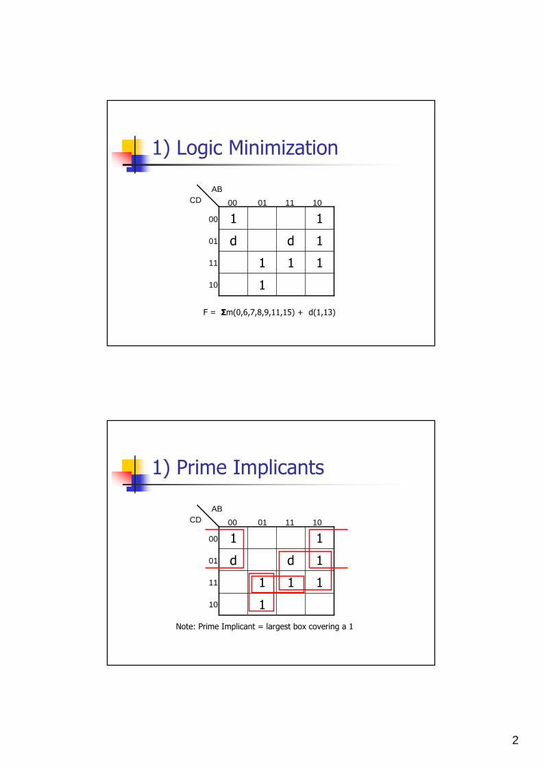
1 CSE 370 Sample Final Exam Questions 1) Logic Minimization CD AB 00 01 11 10 00 01 11 10 F = Σm(0,6,7,8,9,11,15) + d(1,13)
Transcript of CSE 370 Sample Final Exam Questions · Sample Final Exam Questions 1) Logic Minimization CD AB ......
1
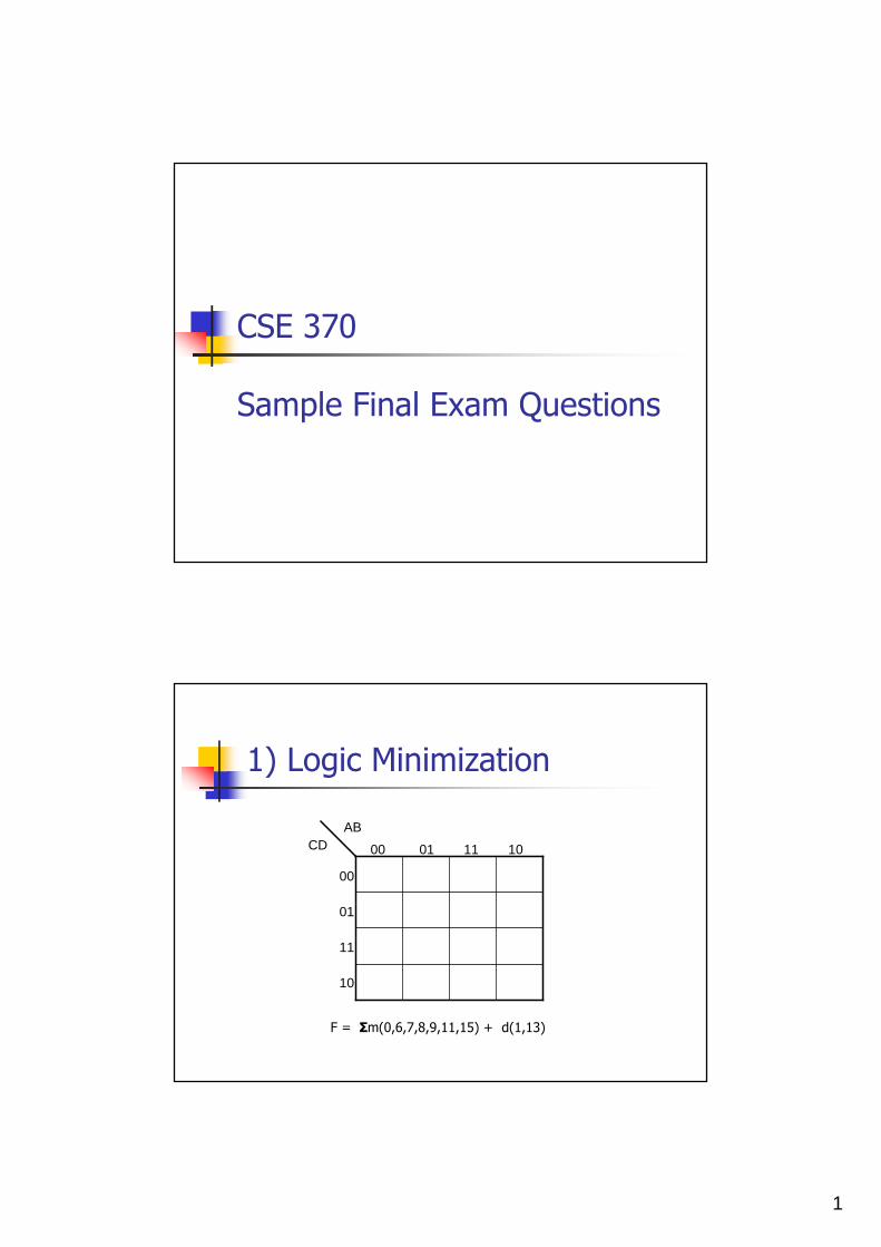
CSE 370
Sample Final Exam Questions
1) Logic Minimization
CDAB
00 01 11 10
00
01
11
10
F = Σm(0,6,7,8,9,11,15) + d(1,13)
2
1) Logic Minimization
1
111
1dd
11
CDAB
00 01 11 10
00
01
11
10
F = Σm(0,6,7,8,9,11,15) + d(1,13)
1) Prime Implicants
1
111
1dd
11
CDAB
00 01 11 10
00
01
11
10
Note: Prime Implicant = largest box covering a 1
3
1) Essential PI’s
1
111
1dd
11
CDAB
00 01 11 10
00
01
11
10
Note: Essential PI = PI’s that cover a 1 not covered by any other PI’s
1) Logic Minimization
1
111
1dd
11
CDAB
00 01 11 10
00
01
11
10
Prime Implicants: B’C’, AD, A’BC, BCD
Essential Prime Implicants: B’C’, AD, A’BC
Minimal Cover: F = B’C’ + AD + A’BC
4
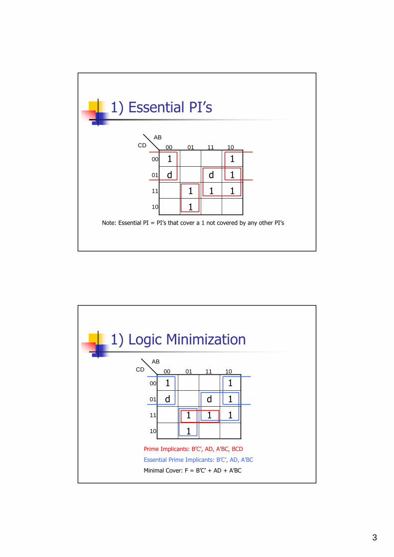
2a) Gates to Functions back into Gates
FG
H
2a) Gates to Functions back into Gates
FG
H
Z = ~(H + G)
Z = ~H & ~G
Z = ~(~(C+D)) & ~(~(F+F))
Z = (C+D) & F
Z = (C+D) & ~(A+B)
Z = (C+D) & ~A & ~B
Z = A’B’C + A’B’D
5
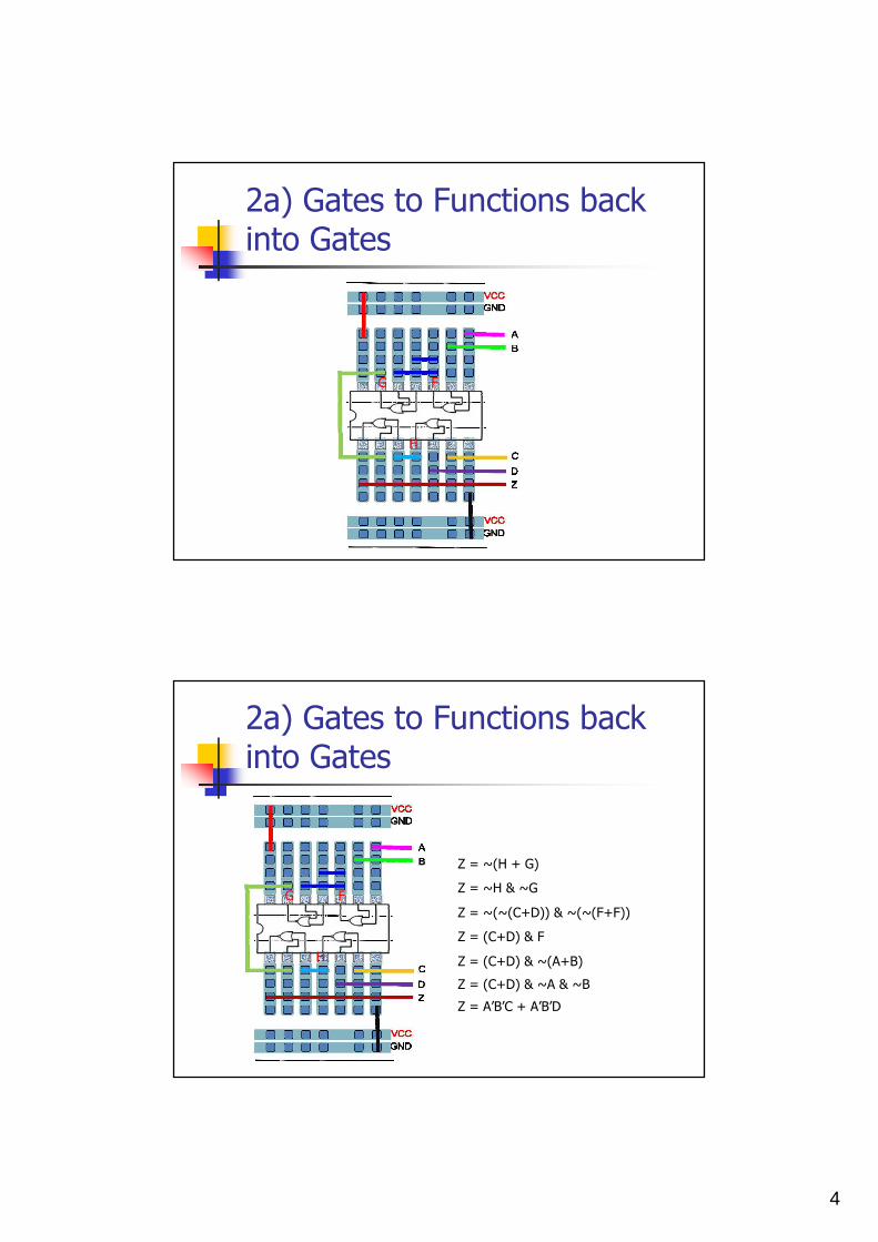
2b) Gates to Functions back into Gates
Z = A’B’C + A’B’DZ = A’B’C + A’B’D
Using deMorgan’s Law…
Z = ~(~(A’B’C) & ~(A’B’D))
C
A’
B’
D
2c) Gates to Functions back into Gates
� NOR Circuit
� 3 gate delays @ 7ns
� 21ns total
� NAND Circuit
� 2 gate delays @ 9ns
� 18ns total
6
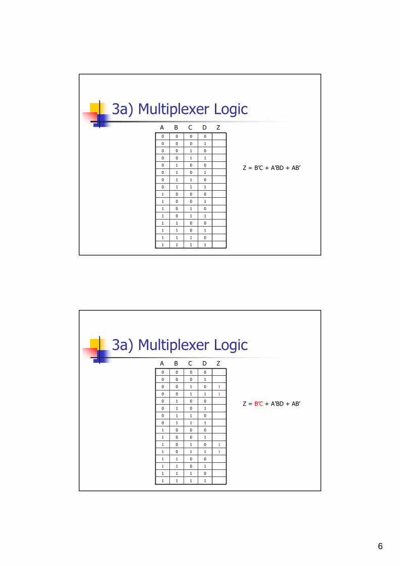
3a) Multiplexer Logic
Z = B’C + A’BD + AB’
1111
0111
1011
0011
1101
0101
1001
0001
1110
0110
1010
0010
1100
0100
1000
0000
A B C D Z
3a) Multiplexer Logic
Z = B’C + A’BD + AB’
1111
0111
1011
0011
11101
10101
1001
0001
1110
0110
1010
0010
11100
10100
1000
0000
A B C D Z
7
3a) Multiplexer Logic
Z = B’C + A’BD + AB’
1111
0111
1011
0011
11101
10101
1001
0001
11110
0110
11010
0010
11100
10100
1000
0000
A B C D Z
3a) Multiplexer Logic
Z = B’C + A’BD + AB’
1111
0111
1011
0011
11101
10101
11001
10001
11110
0110
11010
0010
11100
10100
1000
0000
A B C D Z
8
3a) Multiplexer Logic
Z = B’C + A’BD + AB’
01111
00111
01011
00011
11101
10101
11001
10001
11110
00110
11010
00010
11100
10100
01000
00000
A B C D Z
3b) Multiplexer Logic
0
1
2
3
4
5
6
7
8
9
10
11
12
13
14
15
S3 S2 S1 S0
16:1 MUX Z = B’C + A’BD + AB’
0
0
1
1
0
1
0
1
1
1
1
1
0
0
0
0
A B C D
9
3c) Multiplexer Logic
0
1
2
3
4
5
6
7
S2 S1 S0
8:1 MUX Z = B’C + A’BD + AB’
1
1
Z = B’C + A’BD + AB’
A B C
Z = B’C + A’BD + AB’
1
D
D
1
Z = B’C + A’BD + AB’
1
D
D
1
1
Z = B’C + A’BD + AB’
0
1
D
D
1
1
0
0
Note: Requires no extra logic
4) Decoder Logic
1111
1011
0101
1001
1110
1010
1100
0000
W = (A xor C) + B
A B C W
10
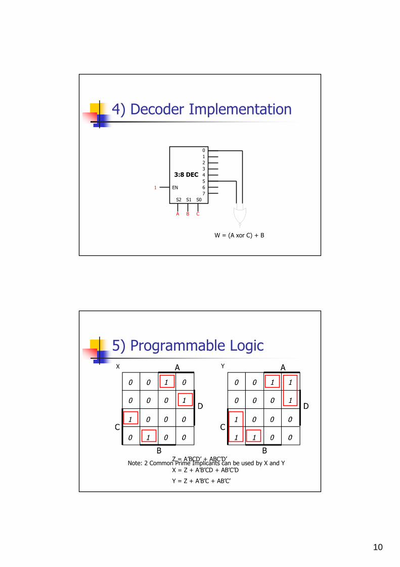
4) Decoder Implementation
0
1
2
3
4
5
6
7
S2 S1 S0
3:8 DEC
A B C
W = (A xor C) + B
EN1
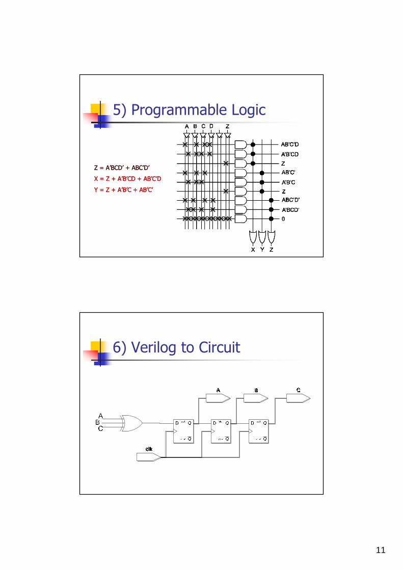
5) Programmable Logic
X Y
Note: 2 Common Prime Implicants can be used by X and YZ = A’BCD’ + ABC’D’
X = Z + A’B’CD + AB’C’D
Y = Z + A’B’C + AB’C’
11
5) Programmable Logic
Z = A’BCD’ + ABC’D’
X = Z + A’B’CD + AB’C’D
Y = Z + A’B’C + AB’C’
Z = A’BCD’ + ABC’D’
X = Z + A’B’CD + AB’C’D
Y = Z + A’B’C + AB’C’
6) Verilog to Circuit
12
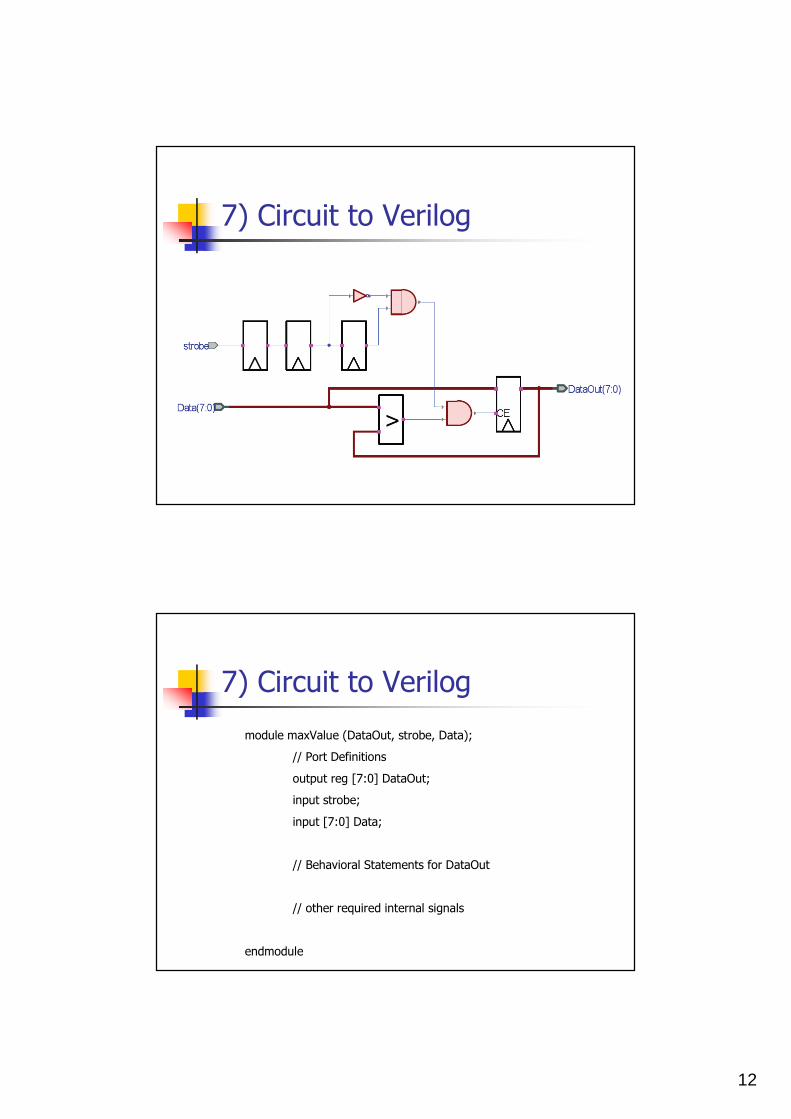
7) Circuit to Verilog
7) Circuit to Verilog
module maxValue (DataOut, strobe, Data);
// Port Definitions
output reg [7:0] DataOut;
input strobe;
input [7:0] Data;
// Behavioral Statements for DataOut
// other required internal signals
endmodule
13
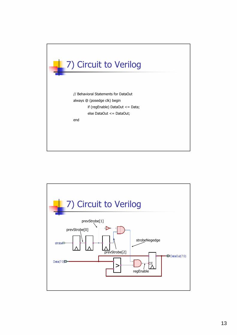
7) Circuit to Verilog
// Behavioral Statements for DataOut
always @ (posedge clk) begin
if (regEnable) DataOut <= Data;
else DataOut <= DataOut;
end
7) Circuit to Verilog
regEnable
strobeNegedge
prevStrobe[2]
prevStrobe[1]
prevStrobe[0]
14
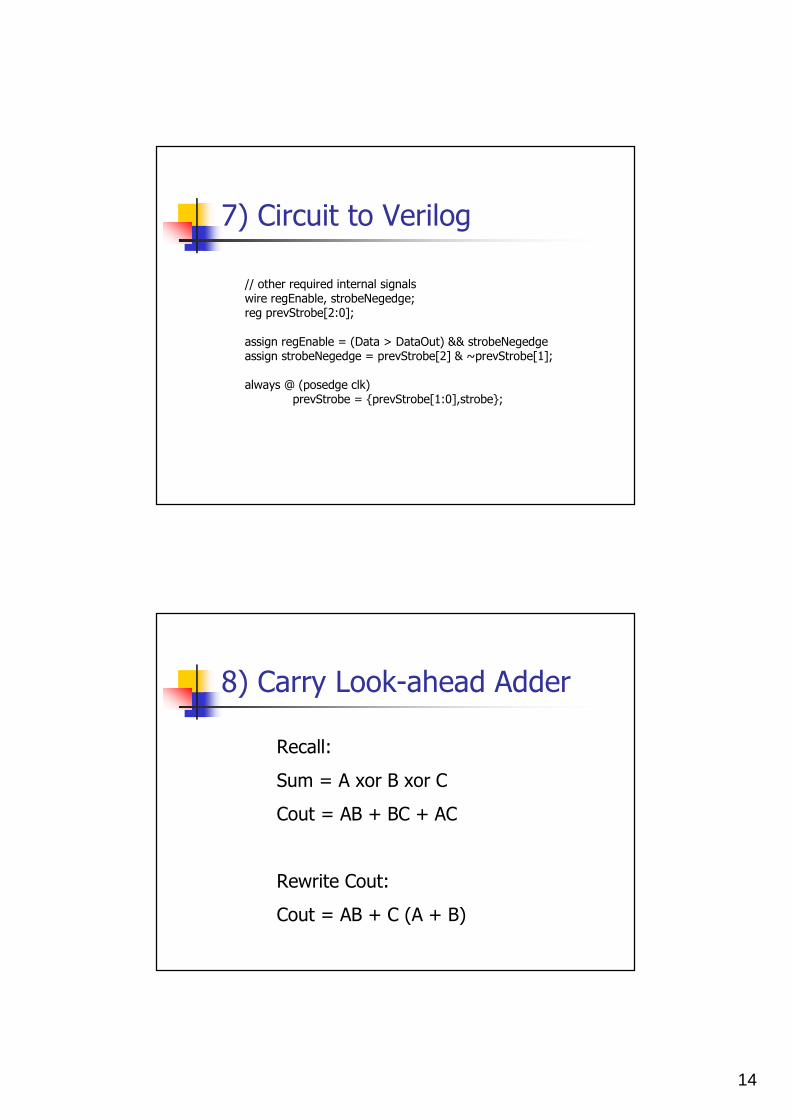
7) Circuit to Verilog
// other required internal signalswire regEnable, strobeNegedge;reg prevStrobe[2:0];
assign regEnable = (Data > DataOut) && strobeNegedgeassign strobeNegedge = prevStrobe[2] & ~prevStrobe[1];
always @ (posedge clk) prevStrobe = {prevStrobe[1:0],strobe};
8) Carry Look-ahead Adder
Recall:
Sum = A xor B xor C
Cout = AB + BC + AC
Rewrite Cout:
Cout = AB + C (A + B)
15
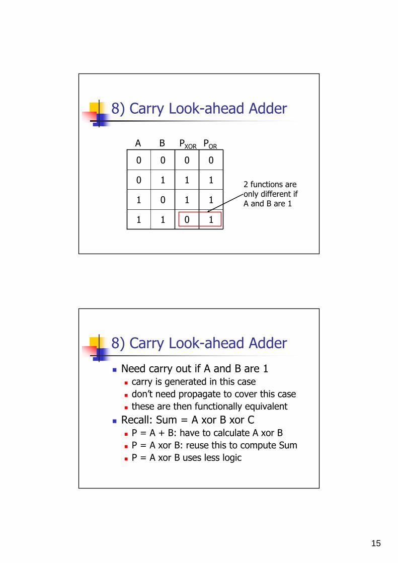
8) Carry Look-ahead Adder
1011
1101
1110
0000
A B PXOR POR
2 functions are only different if A and B are 1
8) Carry Look-ahead Adder
� Need carry out if A and B are 1� carry is generated in this case
� don’t need propagate to cover this case
� these are then functionally equivalent
� Recall: Sum = A xor B xor C� P = A + B: have to calculate A xor B
� P = A xor B: reuse this to compute Sum
� P = A xor B uses less logic
16
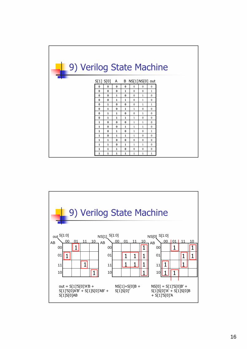
9) Verilog State Machine
1
0
1
0
1
1
1
1
1
0
1
0
0
0
0
0
1
0
1
0
0
0
1
1
0
1
0
1
1
1
0
0
11111
00111
01011
00011
01101
10101
01001
00001
01110
00110
01010
10010
01100
00100
11000
00000
A BS[1] NS[0]NS[1]S[0] out
1111
0111
1011
0011
1101
0101
1001
0001
1110
0110
1010
0010
1100
0100
1000
0000
9) Verilog State Machine
1
1
1
1
S[1:0]
AB 00 01 11 10
00
01
11
10
out
1
111
111
1
00 01 11 10
00
01
11
10
NS[1]
11
11
11
11
00 01 11 10
00
01
11
10
NS[0]S[1:0]
AB
S[1:0]
AB
NS[1]=S[0]B + S[1]S[0]’
NS[0] = S[1]’S[0]B’ + S[1]S[0]’A’ + S[1]S[0]B + S[1]’S[0]’A
out = S[1]’S[0]’A’B + S[1]’S[0]A’B’ + S[1]S[0]’AB’ + S[1]S[0]AB
17
9) Verilog State Machine
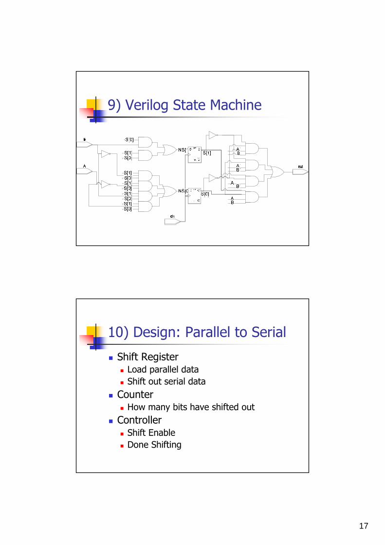
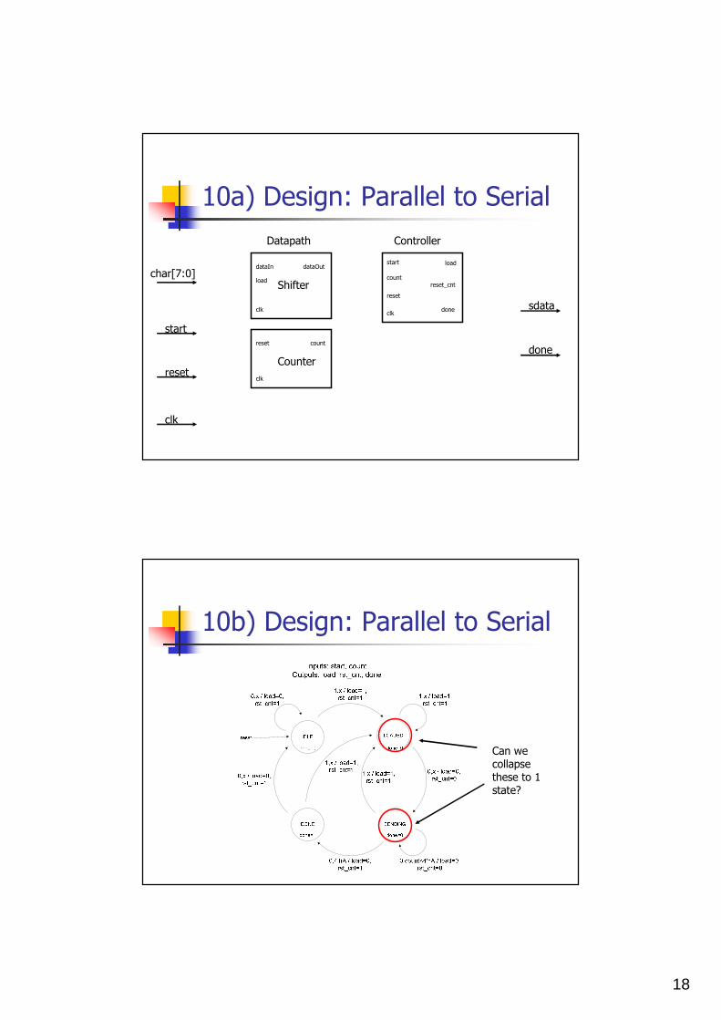
10) Design: Parallel to Serial
� Shift Register� Load parallel data
� Shift out serial data
� Counter� How many bits have shifted out
� Controller� Shift Enable
� Done Shifting
18
10a) Design: Parallel to Serial
Shifter
dataIn
load
dataOut
Counter
reset
clk
count
char[7:0]
start
reset
clk
clk
Controller
clksdata
done
Datapath
start
reset
count
load
reset_cnt
done
10b) Design: Parallel to Serial
Can we collapse these to 1 state?
19
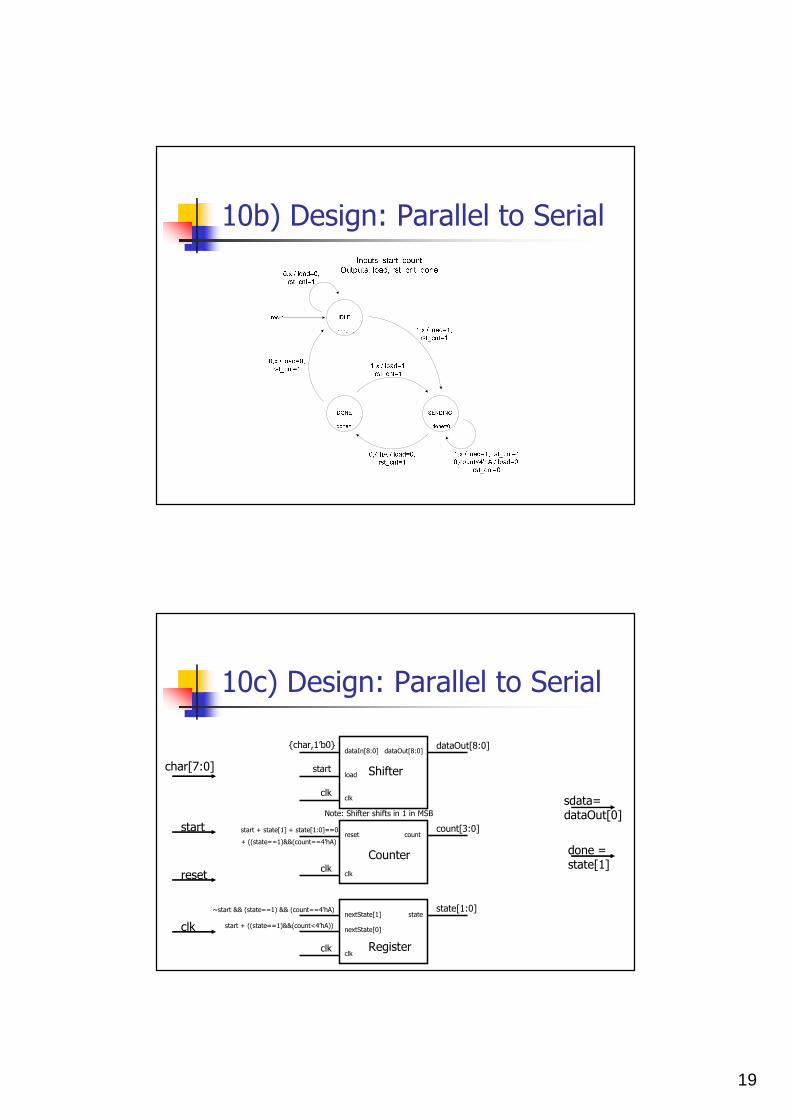
10b) Design: Parallel to Serial
10c) Design: Parallel to Serial
Shifter
dataIn[8:0]
load
dataOut[8:0]
Counter
reset
clk
count
clk sdata= dataOut[0]
done = state[1]
{char,1’b0}
start
clk
dataOut[8:0]
Register
nextState[1]
clk
state
Note: Shifter shifts in 1 in MSB
clk
count[3:0]
clk
state[1:0]
start + state[1] + state[1:0]==0
+ ((state==1)&&(count==4’hA)
~start && (state==1) && (count==4’hA)
nextState[0]start + ((state==1)&&(count<4’hA))
char[7:0]
start
reset
clk
20
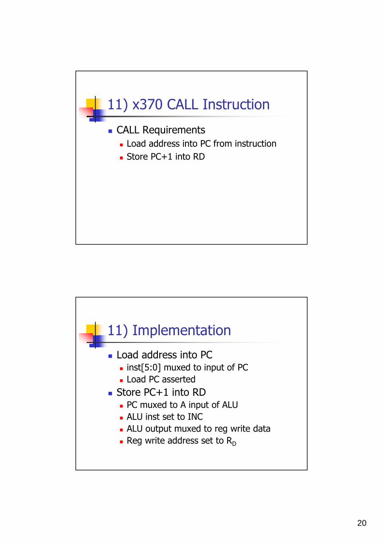
11) x370 CALL Instruction
� CALL Requirements
� Load address into PC from instruction
� Store PC+1 into RD
11) Implementation
� Load address into PC� inst[5:0] muxed to input of PC
� Load PC asserted
� Store PC+1 into RD� PC muxed to A input of ALU
� ALU inst set to INC
� ALU output muxed to reg write data
� Reg write address set to RD

21
Final Notes
� Homework 9� Due today 5:30 pm
� Can accept until Sunday 5:30 if dropboxdoesn’t close
� Final Exam� Wednesday June 9, 8:30-10:20
� EEB 045
� Don’t be late!!!
Final Questions?