Crystallinity Investigation of Compositionally Graded SiGe ... · e-mail: [email protected]...
5
The 5th International Symposium on Advanced Science and Technology of Silicon Materials (JSPS Si Symposium, Abstracts), Nov. 10-14, 2008, Kona, Hawaii, USA Sample-A Sample-B Strained Si layer Thickness (nm) 9.3 9.3 Maximum Ge concentration at top SiGe step (%) 13.9 14.1 Graded SiGe layer thickness (nm) 7745 3757 Grading Rate in SiGe layer (Ge% μm –1 ) 1.8 3.7 Sample-A Sample-B Strained Si layer Thickness (nm) 9.3 9.3 Maximum Ge concentration at top SiGe step (%) 13.9 14.1 Graded SiGe layer thickness (nm) 7745 3757 Grading Rate in SiGe layer (Ge% μm –1 ) 1.8 3.7 Table I. Construction of s-Si wafers evaluated by SIMS. Sample-A Sample-B Strained Si layer Thickness (nm) 9.3 9.3 Maximum Ge concentration at top SiGe step (%) 13.9 14.1 Graded SiGe layer thickness (nm) 7745 3757 Grading Rate in SiGe layer (Ge% μm –1 ) 1.8 3.7 Sample-A Sample-B Strained Si layer Thickness (nm) 9.3 9.3 Maximum Ge concentration at top SiGe step (%) 13.9 14.1 Graded SiGe layer thickness (nm) 7745 3757 Grading Rate in SiGe layer (Ge% μm –1 ) 1.8 3.7 Table I. Construction of s-Si wafers evaluated by SIMS. Crystallinity Investigation of Compositionally Graded SiGe Layers by Synchrotron X-ray Cross-Sectional Diffraction Takeshi Senda 1, 2 , Koji Izunome 1 , Yoshiyuki Tsusaka 2 , Kazunori Fukuda 2 , Kazuki Hayashi 2 , Maiko Abe 2 , Sayuri Takahata 2 , Hidekazu Takano 2 , Yasushi Kagoshima 2 , and Junji Matsui 2 1 Covalent Materials Corporation, 6-861-5 Higashi-ko, Niigata 957-0197, Japan 2 Graduate School of Material Science, University of Hyogo, 3-2-1 Koto, Kamigori, Hyogo 678-1297, Japan e-mail: [email protected] [email protected] [email protected] [email protected] [email protected] [email protected] Abstract We have investigated the crystallinity of compositionally graded SiGe layers of strained Si wafers (s-Si) in the growth direction by irradiating a synchrotron X-ray microbeam with a high parallelism on a cross section of s-Si wafers. As a result, we can confirm the presence of surface parallel SiGe lattice rotation and lattice rotation distribution (LRD). The surface parallel LRD and relaxation ratio of SiGe start to decrease in the depth direction below approximately 3 μm from the wafer surface. It is inferred that the insufficient relaxation of SiGe near the wafer surface is caused by the characteristics of the free wafer surface. Furthermore, such characteristics are thought to lead to a reduction in LRD near the wafer surface. 1. Introduction Many researchers have studied the crystallinity of epitaxially grown SiGe layers. Moreover, it is reported that SiGe layers have a large lattice tilt variation distribution (LTVD), and s-Si 2-6) grown on SiGe layers also inherits this LTVD. 7) However, the crystallinity aggravation mechanism of the micron order in the growth direction for compositionally graded SiGe layers has not yet been elucidated. In this study, we have investigated the crystallinity of compositionally graded SiGe layers of s-Si wafers in the growth direction by irradiating a synchrotron X-ray microbeam with a high parallelism on a cross section of the s-Si wafers. 2. Experiment 2.1 Sample preparation SiGe and s-Si epitaxy was carried out in a commercial single-wafer chemical vapor deposition (CVD) epitaxial reactor at a low pressure (15 Torr). A p-type single Si(001) crystal substrate with a diameter of 200 mm was used. Initially, the Si substrate was ramped and maintained at 1000 ºC to remove Si native oxides and carbon from the substrate surface. Subsequently, SiGe and Si were successively deposited on the Si substrate. The source gases employed for Ge and Si were GeH 4 and SiH 4 , respectively, with H 2 as the carrier gas. The compositionally graded SiGe layers have a stepwise structure that facilitates the investigation of the crystallinity of each SiGe step in the growth direction. The growth temperature of the SiGe layers was 900 ºC, and the Ge concentration varied from 0% on the Si substrate to 14% at the top SiGe layer. Next, s-Si layers with a thickness of approximately 9 nm were deposited on the SiGe layers at 750 ºC. The Ge
Transcript of Crystallinity Investigation of Compositionally Graded SiGe ... · e-mail: [email protected]...
The 5th International Symposium on Advanced Science and Technology of Silicon Materials (JSPS Si Symposium, Abstracts), Nov. 10-14, 2008, Kona, Hawaii, USA
Sample-ASample-B
Strained Si layerThickness
(nm)
9.39.3
Maximum Geconcentration
at top SiGe step(%)
13.914.1
Graded SiGelayer thickness
(nm)
77453757
Grading Ratein SiGe layer(Ge% μm–1)
1.83.7
Sample-ASample-B
Strained Si layerThickness
(nm)
9.39.3
Maximum Geconcentration
at top SiGe step(%)
13.914.1
Graded SiGelayer thickness
(nm)
77453757
Grading Ratein SiGe layer(Ge% μm–1)
1.83.7
Table I. Construction of s-Si wafers evaluated by SIMS.
Sample-ASample-B
Strained Si layerThickness
(nm)
9.39.3
Maximum Geconcentration
at top SiGe step(%)
13.914.1
Graded SiGelayer thickness
(nm)
77453757
Grading Ratein SiGe layer(Ge% μm–1)
1.83.7
Sample-ASample-B
Strained Si layerThickness
(nm)
9.39.3
Maximum Geconcentration
at top SiGe step(%)
13.914.1
Graded SiGelayer thickness
(nm)
77453757
Grading Ratein SiGe layer(Ge% μm–1)
1.83.7
Table I. Construction of s-Si wafers evaluated by SIMS.
Crystallinity Investigation of Compositionally Graded SiGe Layers by Synchrotron X-ray Cross-Sectional Diffraction Takeshi Senda1, 2, Koji Izunome1, Yoshiyuki Tsusaka2, Kazunori Fukuda2, Kazuki Hayashi2, Maiko Abe2, Sayuri Takahata2, Hidekazu Takano2, Yasushi Kagoshima2, and Junji Matsui2
1 Covalent Materials Corporation, 6-861-5 Higashi-ko, Niigata 957-0197, Japan 2 Graduate School of Material Science, University of Hyogo, 3-2-1 Koto, Kamigori, Hyogo 678-1297, Japan
e-mail: [email protected] [email protected] [email protected]
[email protected] [email protected] [email protected]
Abstract
We have investigated the crystallinity of compositionally graded SiGe layers of strained Si wafers (s-Si) in the
growth direction by irradiating a synchrotron X-ray microbeam with a high parallelism on a cross section of s-Si
wafers. As a result, we can confirm the presence of surface parallel SiGe lattice rotation and lattice rotation
distribution (LRD). The surface parallel LRD and relaxation ratio of SiGe start to decrease in the depth direction
below approximately 3 μm from the wafer surface. It is inferred that the insufficient relaxation of SiGe near the
wafer surface is caused by the characteristics of the free wafer surface. Furthermore, such characteristics are thought
to lead to a reduction in LRD near the wafer surface.
1. Introduction
Many researchers have studied the crystallinity of epitaxially grown SiGe layers. Moreover, it is reported that SiGe
layers have a large lattice tilt variation distribution (LTVD), and s-Si 2-6) grown on SiGe layers also inherits this
LTVD. 7) However, the crystallinity aggravation mechanism of the micron order in the growth direction for
compositionally graded SiGe layers has not yet been elucidated. In this study, we have investigated the crystallinity
of compositionally graded SiGe layers of s-Si wafers in the growth direction by irradiating a synchrotron X-ray
microbeam with a high parallelism on a cross section of the s-Si wafers.
2. Experiment
2.1 Sample preparation
SiGe and s-Si epitaxy was carried out in a commercial
single-wafer chemical vapor deposition (CVD) epitaxial
reactor at a low pressure (15 Torr). A p-type single
Si(001) crystal substrate with a diameter of 200 mm was used. Initially, the Si substrate was ramped and maintained
at 1000 ºC to remove Si native oxides and carbon from the substrate surface. Subsequently, SiGe and Si were
successively deposited on the Si substrate. The source gases employed for Ge and Si were GeH4 and SiH4,
respectively, with H2 as the carrier gas. The compositionally graded SiGe layers have a stepwise structure that
facilitates the investigation of the crystallinity of each SiGe step in the growth direction. The growth temperature of
the SiGe layers was 900 ºC, and the Ge concentration varied from 0% on the Si substrate to 14% at the top SiGe
layer. Next, s-Si layers with a thickness of approximately 9 nm were deposited on the SiGe layers at 750 ºC. The Ge
The 5th International Symposium on Advanced Science and Technology of Silicon Materials (JSPS Si Symposium, Abstracts), Nov. 10-14, 2008, Kona, Hawaii, USA
concentration depth profiles for the s-Si wafers were evaluated by secondary ion mass spectroscopy (SIMS). Table 1
and Fig. 1 show, respectively, the details of the SiGe structure and the Ge concentration depth profiles of the s-Si
wafers obtained by SIMS. Two samples—Sample-A and
Sample-B—with different grading rates in the SiGe layers were
prepared. The average Ge concentrations at the top SiGe steps
of Sample-A and Sample-B obtained by SIMS were 13.9% and
14.1%, respectively. On the other hand, the grading rates in the
SiGe layer of Sample-A and Sample-B were 1.8 and 3.7 Ge%
μm–1, respectively.
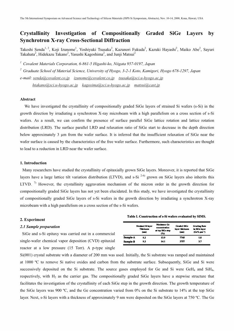
2.2 Incident X-ray optics
The synchrotron X-ray microbeam was constructed in hatch
C2 of BL24XU in SPring-8. 8) The experimental arrangement
of the microbeam optics is schematically illustrated in Fig. 2. 9)
The synchrotron radiation generated by a figure-8 undulator
was monochromatized to 15 keV using a Si double crystal
monochromator of the horizontal dispersion type with 111
symmetric reflections. The X-ray microbeam was primarily
focused in the vertical direction on the sample surface using an
Rh-coated bent cylindrical mirror for analyzing each step of the
compositionally graded SiGe layers more precisely. As a result,
the beam size was 3.9 μm (H) × 0.8 μm (V), and the angular
divergence in the horizontal direction was 2.2 arcsec on the
specimen.
2.3 Measurement procedure
First, in order to determine the thickness of the SiGe layer, we acquired contour maps of the 440 reflection
intensity distribution from a set of -scans (rocking curves) at each position in the vertical direction (Z). Next, by
putting the analyzer crystal behind the specimen, as shown in Fig. 2, we confirmed the center depth of each SiGe
step by the Z-scan. Here, we define the center depth of each SiGe step determined by the Z -scan as the depth of each
SiGe step. The 2 - scan of 440 reflections was successively performed at the depth of each SiGe step. The lattice
constants of the SiGe layers were determined by the above-mentioned 2 peak positions of each SiGe step. The
relaxation ratio of each SiGe step was calculated by lattice constants of the fully relaxed SiGe obtained from
Vegard’s law and the average Ge concentration of each SiGe step obtained by SIMS. The rocking curve of the 440
reflection using the analyzer crystal was obtained for the depth of each SiGe step. The central positions of the
rocking curve peaks revealed a SiGe lattice rotation angle (LRA) parallel to the Si substrate surface. On the other
hand, the width of the rocking curve peaks revealed a SiGe lattice rotation distribution (LRD) showing the
distribution range of lattice orientation parallel to the Si substrate surface. In this study, we define the parallel and
vertical directions for the Si substrate surface as “surface parallel” and “surface normal,” respectively. Moreover, the
full width at half maximum (FWHM) of each rocking curve fitted by a Gaussian function is also defined as an LRD.
Fig. 2. Setup of optical system producing a highly parallel X-ray microbeam.
Double CrystalMonochromator
15 keVChannel-Cut Crystals
Si (111)
Four-Quadrant Slit100 (H) 20 (V) μm2
Analyzer Crystal
Bent Cylindrical Mirror
Scintillation Counter
Sample Stage
2
Z
Double CrystalMonochromator
15 keVChannel-Cut Crystals
Si (111)
Four-Quadrant Slit100 (H) 20 (V) μm2
Analyzer Crystal
Bent Cylindrical Mirror
Scintillation Counter
Sample Stage
2
Z
Fig. 1. Ge concentration depth profiles for SiGe layers as function of distance from wafer surface determined by SIMS. The grading rates of Sample-A and Sample-B are 1.8 and 3.7 Ge% μm–1, respectively.
0
5
10
15
20
0 1 2 3 4 5 6 7 8 9 10 Distance from Wafer Surface ( m)
Ge
Con
cent
ratio
n (A
t.%)
Sample-B
Sample-A
Top SiGe step
Graded SiGe layer
Wafer Surface
The 5th International Symposium on Advanced Science and Technology of Silicon Materials (JSPS Si Symposium, Abstracts), Nov. 10-14, 2008, Kona, Hawaii, USA
Fig. 4. Results of 2 - scan for 440 reflections obtained by putting analyzer crystal behind specimen: (a) Sample-A and (b) Sample-B. Each profile was obtained at the depth of a SiGe step.
0.959 0.960 0.961 0.962 0.963 0.964 0.965 0.966101
102
103
104
105Si-sub. 8.5 7.5 6.9 5.6 4.7 3.7 2.6 1.6 0.6
Inte
nsity
(cps
)
Lattice Constant (440)
0.959 0.960 0.961 0.962 0.963 0.964 0.965 0.966101
102
103
104
105Si-sub. 5.5 5.0 4.5 4.1 3.6 3.1 2.0 0.6
Inte
nsity
(cps
)
Lattice Constant (440)
(a) (b)depth (μm)
0.959 0.960 0.961 0.962 0.963 0.964 0.965 0.966101
102
103
104
105Si-sub. 8.5 7.5 6.9 5.6 4.7 3.7 2.6 1.6 0.6
Inte
nsity
(cps
)
Lattice Constant (440)
0.959 0.960 0.961 0.962 0.963 0.964 0.965 0.966101
102
103
104
105Si-sub. 5.5 5.0 4.5 4.1 3.6 3.1 2.0 0.6
Inte
nsity
(cps
)
Lattice Constant (440)
(a) (b)
0.959 0.960 0.961 0.962 0.963 0.964 0.965 0.966101
102
103
104
105Si-sub. 8.5 7.5 6.9 5.6 4.7 3.7 2.6 1.6 0.6
Inte
nsity
(cps
)
Lattice Constant (440)
0.959 0.960 0.961 0.962 0.963 0.964 0.965 0.966101
102
103
104
105Si-sub. 5.5 5.0 4.5 4.1 3.6 3.1 2.0 0.6
Inte
nsity
(cps
)
Lattice Constant (440)
(a) (b)depth (μm)
Fig. 5. Rocking curve results of 440 reflections obtained by putting analyzer crystal behind specimen: (a) Sample-A and (b) Sample-B. The numbers shown indicate the depth of each SiGe step in μm.
-200 -100 0 100 200
5000
10000
15000
Si sub.
depth
5.55.04.5
3.63.1
4.1
0.62.0
Inte
nsity
(cps
)
Lattice Rotation Distribution (arcsec)-200 -100 0 100 200
5000
10000
15000
20000
Si sub.
Inte
nsity
(cps
)
Lattice Rotation Distribution (arcsec)7.56.95.64.73.72.61.6
depth
(a) (b)
-200 -100 0 100 200
5000
10000
15000
Si sub.
depth
5.55.04.5
3.63.1
4.1
0.62.0
Inte
nsity
(cps
)
Lattice Rotation Distribution (arcsec)-200 -100 0 100 200
5000
10000
15000
20000
Si sub.
Inte
nsity
(cps
)
Lattice Rotation Distribution (arcsec)7.56.95.64.73.72.61.6
depth
(a) (b)
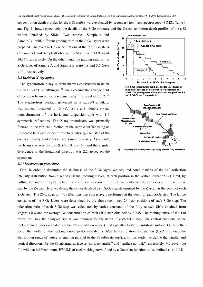
3. Results and Discussion
Figures 3(a) and 3(b) show the contour maps of
the 440 reflection intensity distributions of
Sample-A and Sample-B, respectively. For both
Sample-A and Sample-B, we can confirm that the
peak position of the SiGe layers shifts to the
low-angle side as the Ge concentration in the SiGe
layers increases. Figure 4 shows the results of the
2 - scan of 440 reflection obtained by putting the
analyzer crystal behind the specimen. The vertical
and horizontal axes represent the intensity
detected by a scintillation counter and the (440)
lattice constant equivalent to 2 positions,
respectively. Each profile in the figure was
obtained at the depth of each SiGe step; the depths
are indicated in μm. Figure 5 shows the rocking
curve results of 440 reflection obtained by putting
the analyzer crystal behind the specimen. The
numbers shown in Fig. 5 indicate the depth in
μm of each SiGe step. For both Sample-A and
Sample-B, we can confirm that there are
differences in the peak positions of the rocking
curve between the SiGe layers and the Si
substrate.
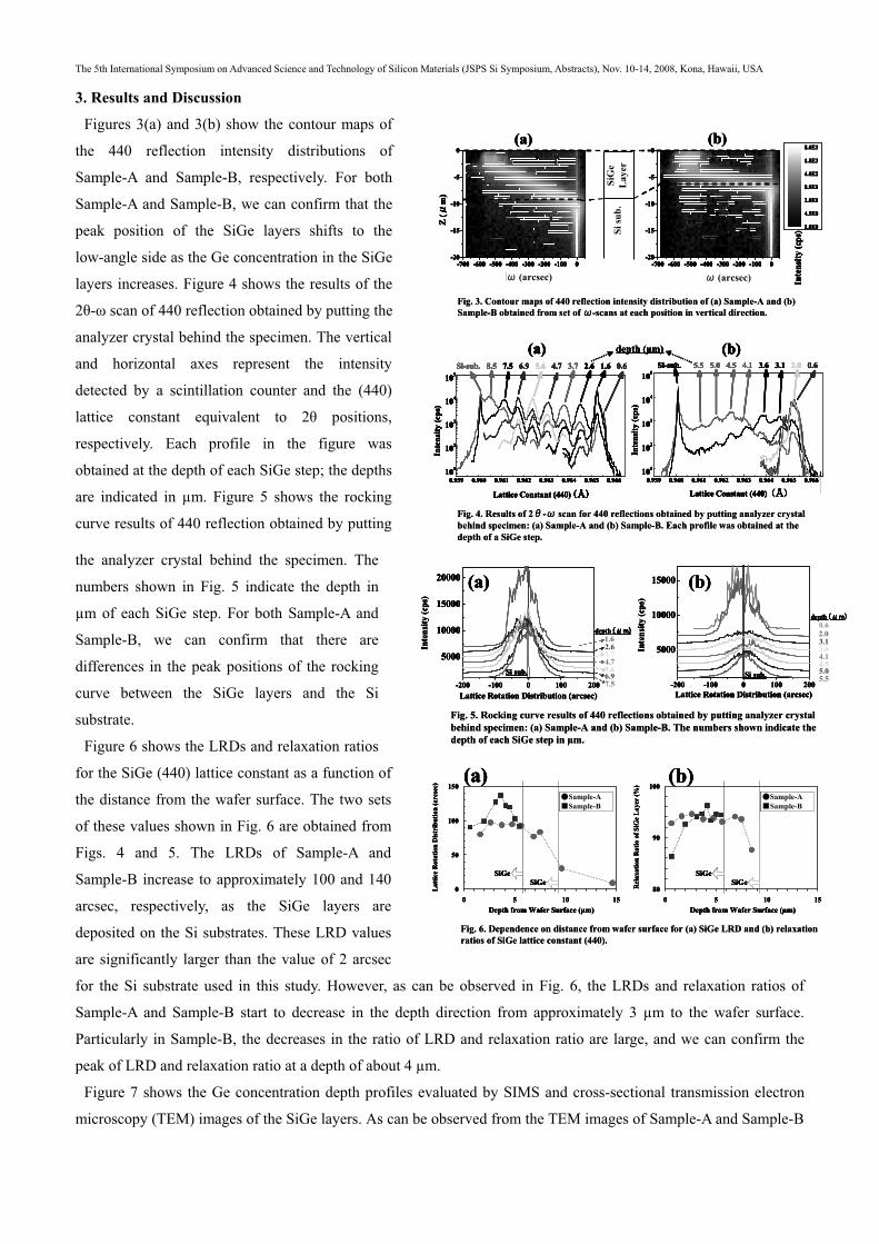
Figure 6 shows the LRDs and relaxation ratios
for the SiGe (440) lattice constant as a function of
the distance from the wafer surface. The two sets
of these values shown in Fig. 6 are obtained from
Figs. 4 and 5. The LRDs of Sample-A and
Sample-B increase to approximately 100 and 140
arcsec, respectively, as the SiGe layers are
deposited on the Si substrates. These LRD values
are significantly larger than the value of 2 arcsec
for the Si substrate used in this study. However, as can be observed in Fig. 6, the LRDs and relaxation ratios of
Sample-A and Sample-B start to decrease in the depth direction from approximately 3 μm to the wafer surface.
Particularly in Sample-B, the decreases in the ratio of LRD and relaxation ratio are large, and we can confirm the
peak of LRD and relaxation ratio at a depth of about 4 μm.
Figure 7 shows the Ge concentration depth profiles evaluated by SIMS and cross-sectional transmission electron
microscopy (TEM) images of the SiGe layers. As can be observed from the TEM images of Sample-A and Sample-B
Fig. 3. Contour maps of 440 reflection intensity distribution of (a) Sample-A and (b) Sample-B obtained from set of -scans at each position in vertical direction.
-700 -600 -500 -400 -300 -200 -100 0-20
-15
-10
-5
0
(arcsec)
Z (
m)
1.0E0
4.5E0
2.0E1
8.9E1
4.0E2
1.8E3
8.0E3
-700 -600 -500 -400 -300 -200 -100 0-20
-15
-10
-5
0
(arcsec)
Z (
m)
1.0E0
4.5E0
2.0E1
8.9E1
4.0E2
1.8E3
8.0E3
SiG
eL
ayer
Si su
b.
Inte
nsity
(cps
)
(arcsec) (arcsec)
(b)(a)
-700 -600 -500 -400 -300 -200 -100 0-20
-15
-10
-5
0
(arcsec)
Z (
m)
1.0E0
4.5E0
2.0E1
8.9E1
4.0E2
1.8E3
8.0E3
-700 -600 -500 -400 -300 -200 -100 0-20
-15
-10
-5
0
(arcsec)
Z (
m)
1.0E0
4.5E0
2.0E1
8.9E1
4.0E2
1.8E3
8.0E3
SiG
eL
ayer
Si su
b.
Inte
nsity
(cps
)
(arcsec) (arcsec)-700 -600 -500 -400 -300 -200 -100 0
-20
-15
-10
-5
0
(arcsec)
Z (
m)
1.0E0
4.5E0
2.0E1
8.9E1
4.0E2
1.8E3
8.0E3
-700 -600 -500 -400 -300 -200 -100 0-20
-15
-10
-5
0
(arcsec)
Z (
m)
1.0E0
4.5E0
2.0E1
8.9E1
4.0E2
1.8E3
8.0E3
SiG
eL
ayer
Si su
b.
Inte
nsity
(cps
)
(arcsec) (arcsec)
(b)(a)
Fig. 6. Dependence on distance from wafer surface for (a) SiGe LRD and (b) relaxation ratios of SiGe lattice constant (440).
80
90
100
0 5 10 15Depth from Wafer Surface (μm)
Rel
axat
ion
Rat
io o
f SiG
e L
ayer
(%)
SiGe
Sample-ASample-B
SiGe0
50
100
150
0 5 10 15Depth from Wafer Surface (μm)
Lat
tice
Rot
atio
n D
istr
ibut
ion
(arc
sec)
SiGe
Sample-ASample-B
SiGe
(a) (b)
80
90
100
0 5 10 15Depth from Wafer Surface (μm)
Rel
axat
ion
Rat
io o
f SiG
e L
ayer
(%)
SiGe
Sample-ASample-B
SiGe0
50
100
150
0 5 10 15Depth from Wafer Surface (μm)
Lat
tice
Rot
atio
n D
istr
ibut
ion
(arc
sec)
SiGe
Sample-ASample-B
SiGe
(a) (b)
The 5th International Symposium on Advanced Science and Technology of Silicon Materials (JSPS Si Symposium, Abstracts), Nov. 10-14, 2008, Kona, Hawaii, USA
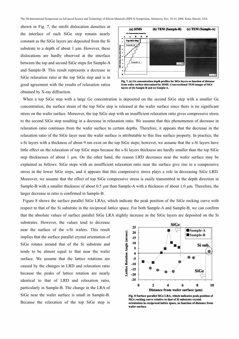
shown in Fig. 7, the misfit dislocation densities at
the interface of each SiGe step remain nearly
constant as the SiGe layers are deposited from the Si
substrate to a depth of about 1 μm. However, these
dislocations are hardly observed at the interface
between the top and second SiGe steps for Sample-A
and Sample-B. This result represents a decrease in
SiGe relaxation ratio at the top SiGe step and is in
good agreement with the results of relaxation ratios
obtained by X-ray diffraction.
When a top SiGe step with a large Ge concentration is deposited on the second SiGe step with a smaller Ge
concentration, the surface strain of the top SiGe step is released at the wafer surface since there is no significant
stress on the wafer surface. Moreover, the top SiGe step with an insufficient relaxation ratio gives compressive stress
to the second SiGe step resulting in a decrease in relaxation ratio. We assume that this phenomenon of decrease in
relaxation ratio continues from the wafer surface to certain depths. Therefore, it appears that the decrease in the
relaxation ratio of the SiGe layer near the wafer surface is attributable to this free surface property. In practice, the
s-Si layers with a thickness of about 9 nm exist on the top SiGe steps; however, we assume that the s-Si layers have
little effect on the relaxation of top SiGe steps because the s-Si layers thickness are hardly smaller than the top SiGe
step thicknesses of about 1 μm. On the other hand, the reason LRD decreases near the wafer surface may be
explained as follows. SiGe steps with an insufficient relaxation ratio near the surface give rise to a compressive
stress in the lower SiGe steps, and it appears that this compressive stress plays a role in decreasing SiGe LRD.
Moreover, we assume that the effect of top SiGe compressive stress is easily transmitted in the depth direction in
Sample-B with a smaller thickness of about 0.5 μm than Sample-A with a thickness of about 1.0 μm. Therefore, the
larger decrease in ratio is confirmed in Sample-B.
Figure 8 shows the surface parallel SiGe LRAs, which indicate the peak position of the SiGe rocking curve with
respect to that of the Si substrate in the reciprocal lattice space. For both Sample-A and Sample-B, we can confirm
that the absolute values of surface parallel SiGe LRA slightly increase as the SiGe layers are deposited on the Si
substrates. However, the values tend to decrease
near the surface of the s-Si wafers. This result
implies that the surface parallel crystal orientation of
SiGe rotates around that of the Si substrate and
tends to be almost equal to that near the wafer
surface. We assume that the lattice rotations are
caused by the changes in LRD and relaxation ratio
because the peaks of lattice rotation are nearly
identical to that of LRD and relaxation ratio,
particularly in Sample-B. The change in the LRA of
SiGe near the wafer surface is small in Sample-B.
Because the relaxation of the top SiGe step is
Fig. 7. (a) Ge concentration depth profiles for SiGe layers as function of distance from wafer surface determined by SIMS. Cross-sectional TEM images of SiGelayers of (b) Sample-B and (c) Sample-A.
0 5 10 15 20
01
23
45
67
89
10 D
istance from W
afer Surface (m
)
Ge Concentration (atomic%)
Sample-B
Sample-A
(b) TEM (Sample-B) (c) TEM (Sample-A)(a) SIMS
Top SiGe Step
0 5 10 15 20
01
23
45
67
89
10 D
istance from W
afer Surface (m
)
Ge Concentration (atomic%)
Sample-B
Sample-A
(b) TEM (Sample-B) (c) TEM (Sample-A)(a) SIMS
Top SiGe Step
Fig. 8 Surface parallel SiGe LRA, which indicates peak position of SiGe rocking curve relative to that of Si substrate crystal orientation in reciprocal lattice space, as function of distance from wafer surface.
-25-20-15-10-505
10152025
0 2 4 6 8 10Distance from wafer surface (μm)
Lat
tice
Rot
atio
n A
ngle
(arc
sec)
Si sub.
SiGe
Sample-ASample-B
SiGe
The 5th International Symposium on Advanced Science and Technology of Silicon Materials (JSPS Si Symposium, Abstracts), Nov. 10-14, 2008, Kona, Hawaii, USA
insufficient, it is thought that the top SiGe step grows along the crystal orientation direction of the lower SiGe step in
an almost pseudomorphic state.
4. Conclusions
We have investigated the crystallinity of compositionally graded SiGe layers of s-Si in the growth direction by
irradiating a synchrotron X-ray microbeam with a high parallelism on a cross section of s-Si wafers. As a result, we
can confirm the presence of surface parallel SiGe lattice rotation and LRD similar to the surface normal SiGe LTVD,
as reported previously. The surface parallel LRD and relaxation ratio of SiGe start to decrease in the depth direction
below approximately 3 μm from the wafer surface. On the other hand, the absolute values of surface parallel SiGe
LRA slightly increase as the SiGe layers are deposited on the Si substrates. However, the values tend to decrease
near the surface of the s-Si wafers. This result implies that the surface parallel crystal orientation of SiGe rotates
around that of the Si substrate and tends to be equal to that near the wafer surface. It is estimated that the insufficient
relaxation of SiGe near the wafer surface is caused by the characteristics of the free wafer surface. Furthermore, such
characteristics are thought to lead to a reduction in LRDs near the wafer surface.
Acknowledgements
We express our appreciation to Mr. Shinichi Mitani and coworkers of NuFlare Technology Inc. for cooperation in
the s-Si epitaxial growth in their machine “HT3000.” This work was performed at SPring-8 with the approval of the
Japan Synchrotron Radiation Research Institute (JASRI) (Proposal No. C03B24XU-5043N).
References
1) T. Hatakeyama, K. Matsuzawa, and S. Takagi: Jpn. J. Appl. Phys. 40 (2001) 2627.
2) E. A. Fitzgerald, Y.-H. Xie, M. L. Green, D. Brasen, A. R. Kortan, J. Michel, Y. –J. Mii, and B. E. Weir: Appl.
Phys. Lett. 59 (1991) 811.
3) G. P. Watson, E. A. Fitzgerald, Y.-H. Xie, and D. Monroe: J. Appl. Phys. 75 (1994) 263.
4) S. B. Samavedam and E. A. Fitzgerald: J. Appl. Phys. 81 (1997) 3108.
5) M. T. Currie, S. B. Samavedam, T. A. Langdo, C. W. Leitz, and E. A. Fitzgerald: Appl. Phys. Lett. 72 (1998)
1718.
6) C. W. Leitz, M. T. Currie, A. Y. Kim, J. L. E. Robbins, and E. A. Fitzgerald: J. Appl. Phys. 90 (2001) 2730.
7) K. Fukuda, N. Tomita, K. Hayashi, Y. Tsusaka, Y. Kagoshima, J. Matsui, and A. Ogura: Jpn. J. Appl. Phys. 45
(2006) 8542.
8) Y. Tsusaka, K. Yokoyama, K. Takai, Y. Kagoshima, and J. Matsui: Nucl. Instrum. Methods Phys. Res. Sect. A
467-468 (2001) 670.
9) S. Takeda, K. Yokoyama, Y. Tsusaka, Y. Kagoshima, J. Matsui, and A. Ogura: J. Synchrotron Radat. 113 (2006) 373.
![arXiv:1102.0031v2 [math.GR] 11 Mar 2014 · arXiv:1102.0031v2 [math.GR] 11 Mar 2014 PROPERTY (T) FOR GROUPS GRADED BY ROOT SYSTEMS MIKHAIL ERSHOV, ANDREI JAIKIN-ZAPIRAIN, AND MARTIN](https://static.fdocument.org/doc/165x107/602acf349cebdf3f5776aa48/arxiv11020031v2-mathgr-11-mar-2014-arxiv11020031v2-mathgr-11-mar-2014.jpg)


![A Wideband 77GHz, 17.5dBm Power Amplifier in Siliconhajimiri/pdf/77GHz PA-Komijani.pdf · SiGe BiCMOS process. ... and automotive radar (e.g., 77GHz band) [1][2][3]. ... approximately](https://static.fdocument.org/doc/165x107/5b57e9367f8b9a657c8b4e29/a-wideband-77ghz-175dbm-power-amplifier-in-hajimiripdf77ghz-pa-komijanipdf.jpg)