

CRD5378 Single-Channel Seismic Reference Design · PDF fileWindows, Windows XP, ... The...
64
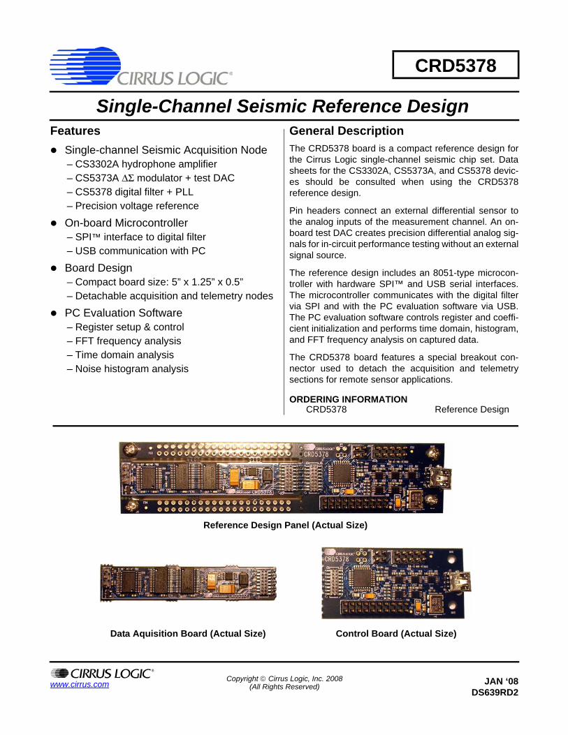
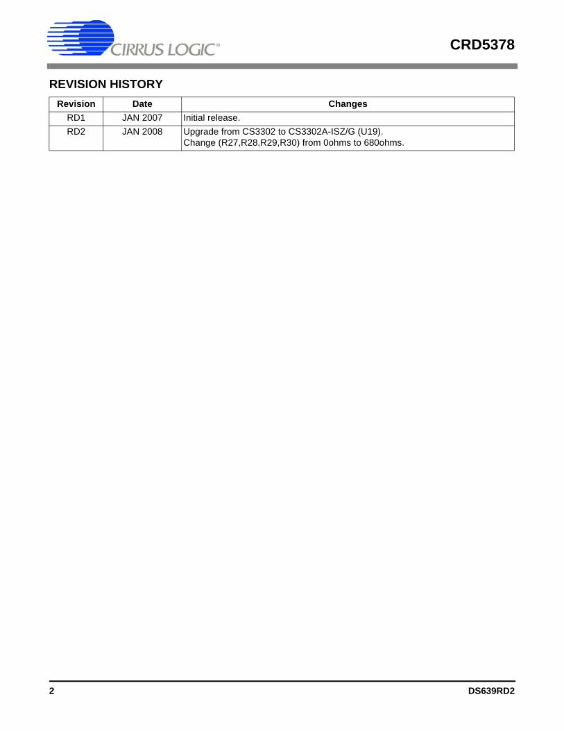
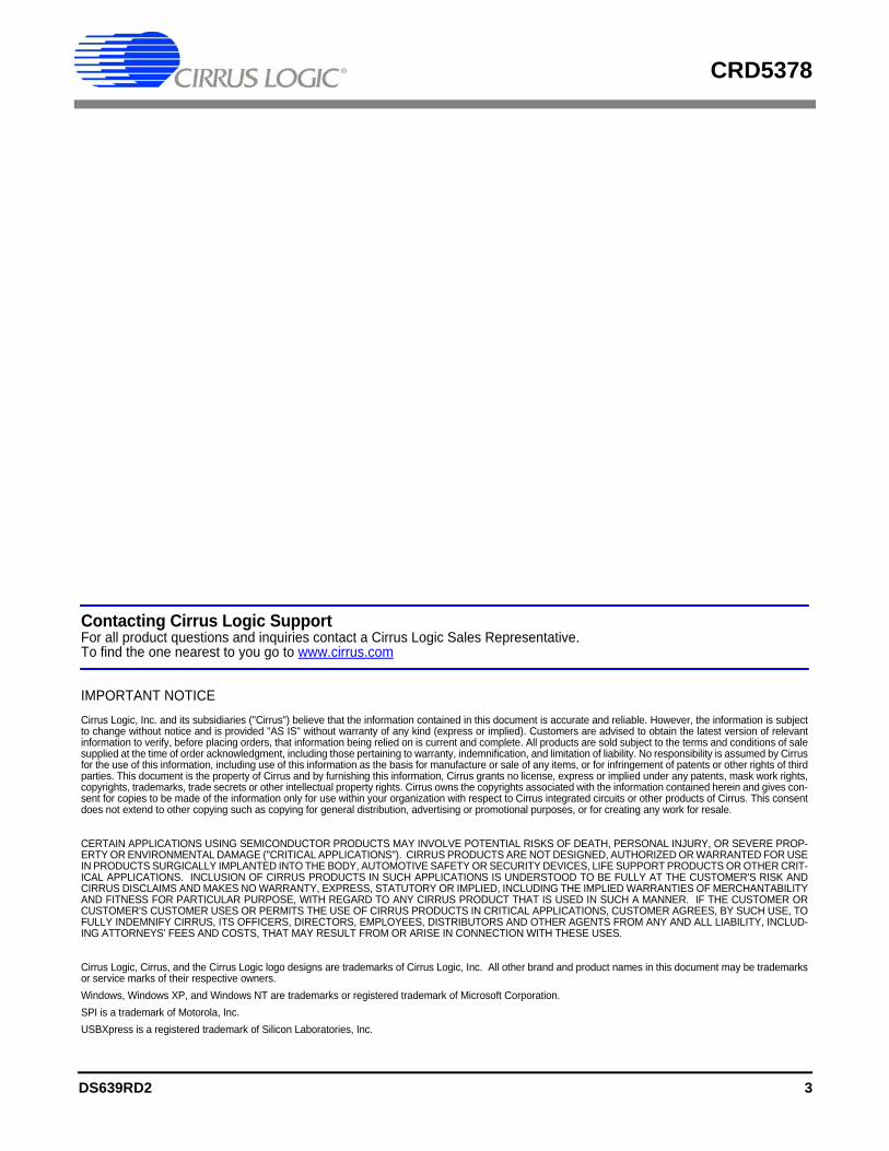
Copyright © Cirrus Logic, Inc. 2008 (All Rights Reserved) www.cirrus.com Reference Design Panel (Actual Size) Data Aquisition Board (Actual Size) Control Board (Actual Size) CRD5378 Single-Channel Seismic Reference Design Features Single-channel Seismic Acquisition Node – CS3302A hydrophone amplifier – CS5373A ∆Σ modulator + test DAC – CS5378 digital filter + PLL – Precision voltage reference On-board Microcontroller – SPI™ interface to digital filter – USB communication with PC Board Design – Compact board size: 5” x 1.25” x 0.5” – Detachable acquisition and telemetry nodes PC Evaluation Software – Register setup & control – FFT frequency analysis – Time domain analysis – Noise histogram analysis General Description The CRD5378 board is a compact reference design for the Cirrus Logic single-channel seismic chip set. Data sheets for the CS3302A, CS5373A, and CS5378 devic- es should be consulted when using the CRD5378 reference design. Pin headers connect an external differential sensor to the analog inputs of the measurement channel. An on- board test DAC creates precision differential analog sig- nals for in-circuit performance testing without an external signal source. The reference design includes an 8051-type microcon- troller with hardware SPI™ and USB serial interfaces. The microcontroller communicates with the digital filter via SPI and with the PC evaluation software via USB. The PC evaluation software controls register and coeffi- cient initialization and performs time domain, histogram, and FFT frequency analysis on captured data. The CRD5378 board features a special breakout con- nector used to detach the acquisition and telemetry sections for remote sensor applications. ORDERING INFORMATION CRD5378 Reference Design JAN ‘08 DS639RD2
Transcript of CRD5378 Single-Channel Seismic Reference Design · PDF fileWindows, Windows XP, ... The...
Copyright © Cirrus Logic, Inc. 2008 (All Rights Reserved)www.cirrus.com
Reference Design Panel (Actual Size)
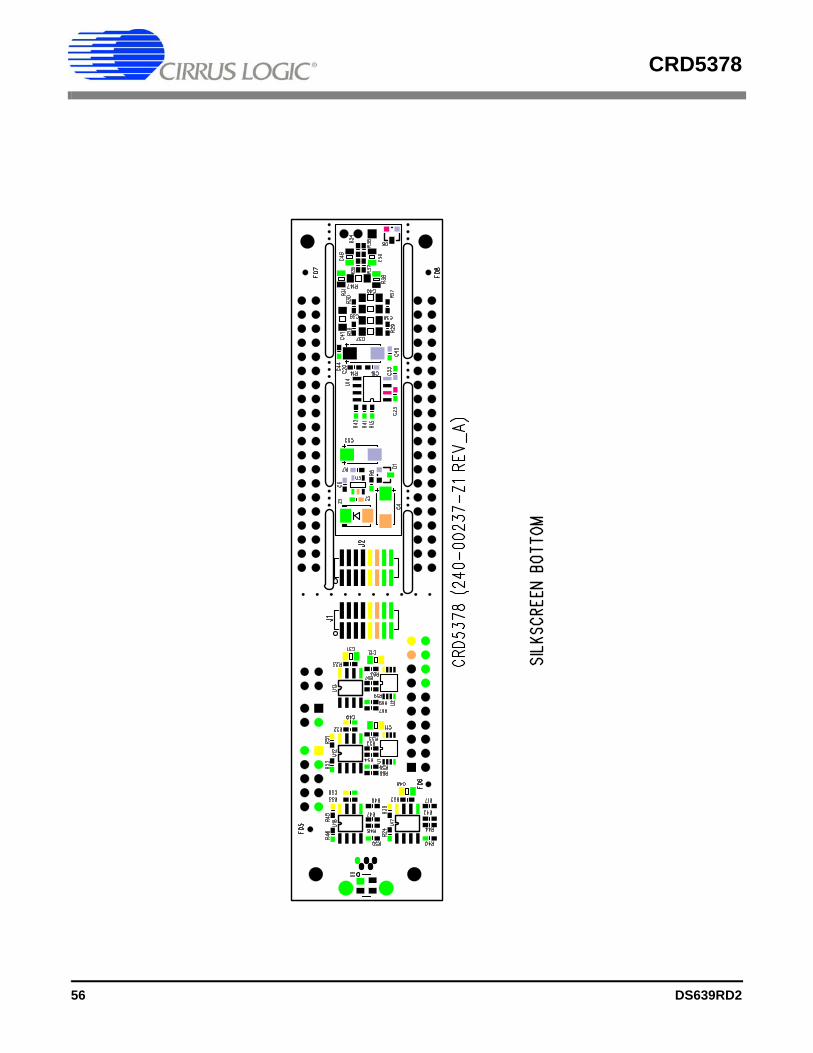
Data Aquisition Board (Actual Size) Control B
CRD5378
Single-Channel Seismic Reference Design
FeaturesSingle-channel Seismic Acquisition Node– CS3302A hydrophone amplifier – CS5373A ∆Σ modulator + test DAC – CS5378 digital filter + PLL– Precision voltage reference
On-board Microcontroller– SPI™ interface to digital filter– USB communication with PC
Board Design– Compact board size: 5” x 1.25” x 0.5”– Detachable acquisition and telemetry nodes
PC Evaluation Software– Register setup & control– FFT frequency analysis– Time domain analysis– Noise histogram analysis
General DescriptionThe CRD5378 board is a compact reference design forthe Cirrus Logic single-channel seismic chip set. Datasheets for the CS3302A, CS5373A, and CS5378 devic-es should be consulted when using the CRD5378reference design.
Pin headers connect an external differential sensor tothe analog inputs of the measurement channel. An on-board test DAC creates precision differential analog sig-nals for in-circuit performance testing without an externalsignal source.
The reference design includes an 8051-type microcon-troller with hardware SPI™ and USB serial interfaces.The microcontroller communicates with the digital filtervia SPI and with the PC evaluation software via USB.The PC evaluation software controls register and coeffi-cient initialization and performs time domain, histogram,and FFT frequency analysis on captured data.
The CRD5378 board features a special breakout con-nector used to detach the acquisition and telemetrysections for remote sensor applications.
ORDERING INFORMATIONCRD5378 Reference Design
oard (Actual Size)
JAN ‘08DS639RD2
CRD5378
REVISION HISTORY Revision Date Changes
RD1 JAN 2007 Initial release.RD2 JAN 2008 Upgrade from CS3302 to CS3302A-ISZ/G (U19).
Change (R27,R28,R29,R30) from 0ohms to 680ohms.
2 DS639RD2
CRD5378
Contacting Cirrus Logic SupportFor all product questions and inquiries contact a Cirrus Logic Sales Representative. To find the one nearest to you go to www.cirrus.com
IMPORTANT NOTICECirrus Logic, Inc. and its subsidiaries ("Cirrus") believe that the information contained in this document is accurate and reliable. However, the information is subjectto change without notice and is provided "AS IS" without warranty of any kind (express or implied). Customers are advised to obtain the latest version of relevantinformation to verify, before placing orders, that information being relied on is current and complete. All products are sold subject to the terms and conditions of salesupplied at the time of order acknowledgment, including those pertaining to warranty, indemnification, and limitation of liability. No responsibility is assumed by Cirrusfor the use of this information, including use of this information as the basis for manufacture or sale of any items, or for infringement of patents or other rights of thirdparties. This document is the property of Cirrus and by furnishing this information, Cirrus grants no license, express or implied under any patents, mask work rights,copyrights, trademarks, trade secrets or other intellectual property rights. Cirrus owns the copyrights associated with the information contained herein and gives con-sent for copies to be made of the information only for use within your organization with respect to Cirrus integrated circuits or other products of Cirrus. This consentdoes not extend to other copying such as copying for general distribution, advertising or promotional purposes, or for creating any work for resale.
CERTAIN APPLICATIONS USING SEMICONDUCTOR PRODUCTS MAY INVOLVE POTENTIAL RISKS OF DEATH, PERSONAL INJURY, OR SEVERE PROP-ERTY OR ENVIRONMENTAL DAMAGE ("CRITICAL APPLICATIONS"). CIRRUS PRODUCTS ARE NOT DESIGNED, AUTHORIZED OR WARRANTED FOR USEIN PRODUCTS SURGICALLY IMPLANTED INTO THE BODY, AUTOMOTIVE SAFETY OR SECURITY DEVICES, LIFE SUPPORT PRODUCTS OR OTHER CRIT-ICAL APPLICATIONS. INCLUSION OF CIRRUS PRODUCTS IN SUCH APPLICATIONS IS UNDERSTOOD TO BE FULLY AT THE CUSTOMER'S RISK ANDCIRRUS DISCLAIMS AND MAKES NO WARRANTY, EXPRESS, STATUTORY OR IMPLIED, INCLUDING THE IMPLIED WARRANTIES OF MERCHANTABILITYAND FITNESS FOR PARTICULAR PURPOSE, WITH REGARD TO ANY CIRRUS PRODUCT THAT IS USED IN SUCH A MANNER. IF THE CUSTOMER ORCUSTOMER'S CUSTOMER USES OR PERMITS THE USE OF CIRRUS PRODUCTS IN CRITICAL APPLICATIONS, CUSTOMER AGREES, BY SUCH USE, TOFULLY INDEMNIFY CIRRUS, ITS OFFICERS, DIRECTORS, EMPLOYEES, DISTRIBUTORS AND OTHER AGENTS FROM ANY AND ALL LIABILITY, INCLUD-ING ATTORNEYS' FEES AND COSTS, THAT MAY RESULT FROM OR ARISE IN CONNECTION WITH THESE USES.
Cirrus Logic, Cirrus, and the Cirrus Logic logo designs are trademarks of Cirrus Logic, Inc. All other brand and product names in this document may be trademarksor service marks of their respective owners.Windows, Windows XP, and Windows NT are trademarks or registered trademark of Microsoft Corporation.SPI is a trademark of Motorola, Inc.USBXpress is a registered trademark of Silicon Laboratories, Inc.
DS639RD2 3
CRD5378
TABLE OF CONTENTS1. INITIAL SETUP ......................................................................................................................... 6
1.1 Kit Contents ....................................................................................................................... 61.2 Hardware Setup ................................................................................................................. 6
1.2.1 Default Jumper Settings ........................................................................................ 71.3 Software Setup .................................................................................................................. 8
1.3.1 PC Requirements .................................................................................................. 81.3.2 Seismic Evaluation Software Installation .............................................................. 81.3.3 USBXpress® Driver Installation ............................................................................ 81.3.4 Launching the Seismic Evaluation Software ......................................................... 9
1.4 Self-Testing CRD5378 ..................................................................................................... 101.4.1 Noise Test ........................................................................................................... 101.4.2 Distortion Test ..................................................................................................... 11
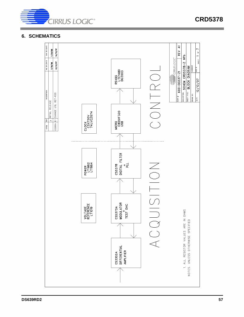
2. HARDWARE DESCRIPTION ................................................................................................. 122.1 Block Diagram ................................................................................................................. 122.2 Analog Hardware ............................................................................................................. 13
2.2.1 Analog Inputs ...................................................................................................... 132.2.2 Differential Amplifiers .......................................................................................... 162.2.3 Delta-Sigma Modulator ....................................................................................... 172.2.4 Delta-Sigma Test DAC ........................................................................................ 182.2.5 Voltage Reference .............................................................................................. 18
2.3 Digital Hardware .............................................................................................................. 192.3.1 Digital Filter ......................................................................................................... 192.3.2 Microcontroller .................................................................................................... 222.3.3 RS-485 Telemetry ............................................................................................... 242.3.4 UART Connection ............................................................................................... 262.3.5 External Connector ............................................................................................. 27
2.4 Power Supplies ................................................................................................................ 272.4.1 Analog Voltage Regulators ................................................................................. 27
2.5 PCB Layout ...................................................................................................................... 282.5.1 Layer Stack ......................................................................................................... 282.5.2 Differential Pairs .................................................................................................. 282.5.3 Bypass Capacitors .............................................................................................. 30
3. SOFTWARE DESCRIPTION .................................................................................................. 313.1 Menu Bar ......................................................................................................................... 313.2 About Panel ..................................................................................................................... 323.3 Setup Panel ..................................................................................................................... 33
3.3.1 USB Port ............................................................................................................. 343.3.2 Digital Filter ......................................................................................................... 353.3.3 Analog Front End ................................................................................................ 363.3.4 Test Bit Stream ................................................................................................... 363.3.5 Gain/Offset .......................................................................................................... 373.3.6 Data Capture ....................................................................................................... 383.3.7 External Macros .................................................................................................. 39
3.4 Analysis Panel ................................................................................................................. 403.4.1 Test Select .......................................................................................................... 413.4.2 Statistics .............................................................................................................. 423.4.3 Cursor ................................................................................................................. 423.4.4 Zoom ................................................................................................................... 433.4.5 Refresh ................................................................................................................ 433.4.6 Harmonics ........................................................................................................... 433.4.7 Spot Noise ........................................................................................................... 43
4 DS639RD2
CRD5378
3.4.8 Plot Error ............................................................................................................. 433.5 Control Panel ................................................................................................................... 44
3.5.1 DF Registers ....................................................................................................... 453.5.2 DF Commands .................................................................................................... 453.5.3 SPI ...................................................................................................................... 453.5.4 Macros ................................................................................................................ 463.5.5 GPIO ................................................................................................................... 463.5.6 Customize ........................................................................................................... 473.5.7 External Macros .................................................................................................. 47
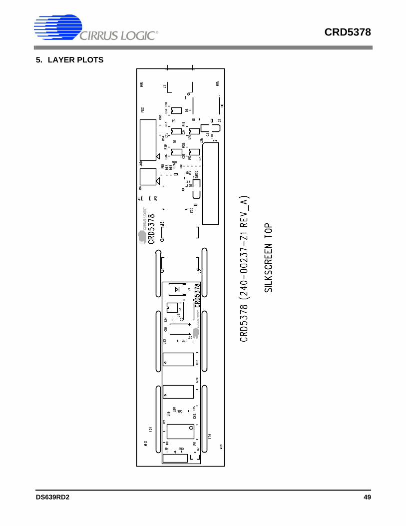
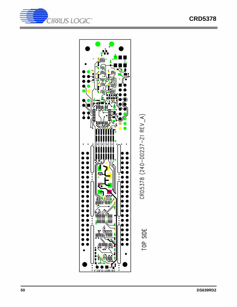
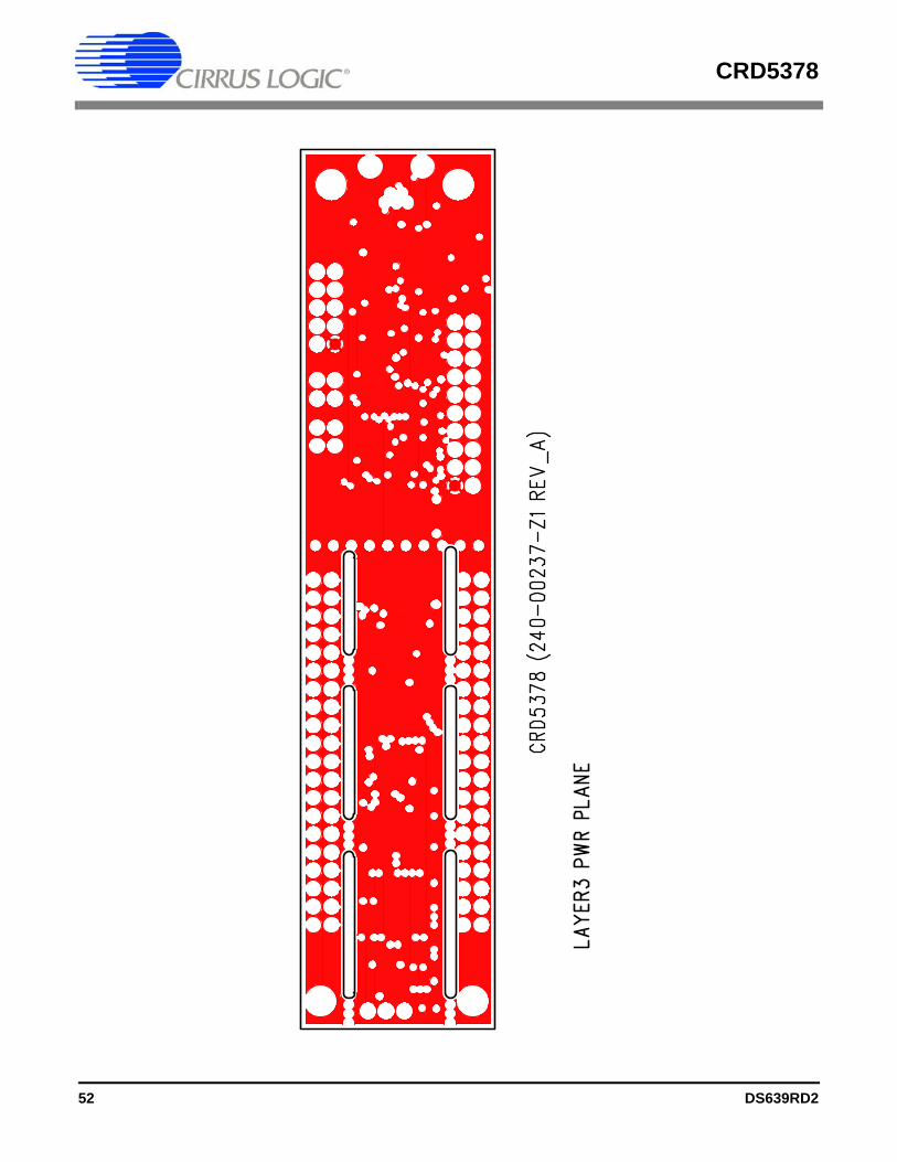
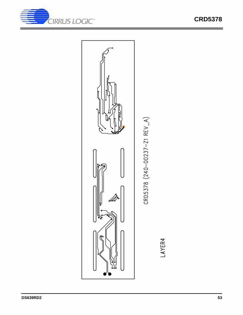
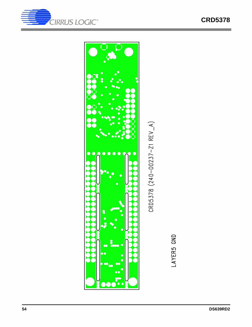
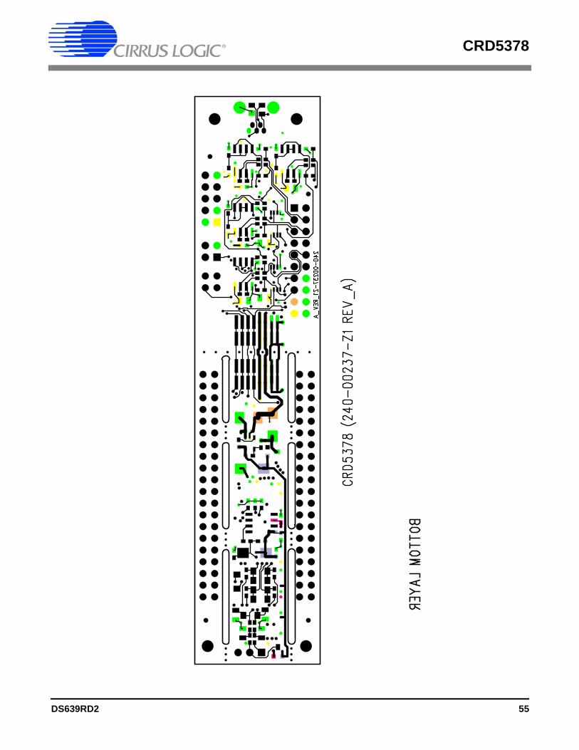
4. BILL OF MATERIALS ........................................................................................................... 485. LAYER PLOTS ...................................................................................................................... 496. SCHEMATICS ....................................................................................................................... 57
LIST OF FIGURESFigure 1. CRD5378 Block Diagram............................................................................................... 12Figure 2. Differential Pair Routing ................................................................................................. 29Figure 3. Quad Group Routing...................................................................................................... 29Figure 4. Bypass Capacitor Placement......................................................................................... 30
LIST OF TABLESTable 1. Amplifier Pin 13 Jumper Setting........................................................................................ 7Table 2. System Clock Input Setting ............................................................................................... 7Table 3. CS5378 PLL Mode Select Setting (R15, R41, R42) ......................................................... 7Table 4. Input SYNC Source Selection Setting............................................................................... 7Table 5. CS5378 SYNC Source Selection Setting.......................................................................... 7Table 6. Pin Header Input Connections ........................................................................................ 13Table 7. Amplifier Pin 13 Resistor Settings................................................................................... 16
DS639RD2 5
CRD5378
1. INITIAL SETUP1.1 Kit ContentsThe CRD5378 reference design kit includes:
• CRD5378 reference design board• USB cable (A to mini-B)• Software download information card
The following are required to operate CRD5378, and are not included:
• Bipolar power supply with clip lead outputs (+/- 3.3 V @ 100 mA)• PC running Windows 2000™ or Windows XP® with an available USB port• Internet access to download the evaluation software
1.2 Hardware SetupTo set up the CRD5378 reference design hardware:
• Verify all jumpers are in the default settings (see next section).• With power off, connect the CRD5378 power inputs to the power supply outputs.
J26 pin 17 = -3.3 VJ26 pin 19 = +3.3 VJ26 pin 20 = 0 V
• Connect the USB cable between the CRD5378 USB connector and the PC USB port.• Proceed to the Software Setup section to install the evaluation software and USB driver.
6 DS639RD2
CRD5378
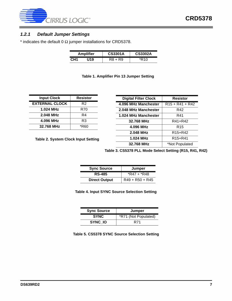
1.2.1 Default Jumper Settings* indicates the default 0 Ω jumper installations for CRD5378.
Amplifier CS3301A CS3302ACH1 U19 R8 + R9 *R10
Table 1. Amplifier Pin 13 Jumper Setting
Input Clock ResistorEXTERNAL CLOCK R2
1.024 MHz R702.048 MHz R44.096 MHz R332.768 MHz *R60
Table 2. System Clock Input Setting
Digital Filter Clock Resistor4.096 MHz Manchester R15 + R41 + R422.048 MHz Manchester R421.024 MHz Manchester R41
32.768 MHz R41+R424.096 MHz R152.048 MHz R15+R421.024 MHz R15+R4132.768 MHz *Not Populated
Table 3. CS5378 PLL Mode Select Setting (R15, R41, R42)
Sync Source JumperRS-485 *R47 + *R48
Direct Output R49 + R50 + R45
Table 4. Input SYNC Source Selection Setting
Sync Source JumperSYNC *R71 (Not Populated)
SYNC_IO R71
Table 5. CS5378 SYNC Source Selection Setting
DS639RD2 7
CRD5378
1.3 Software Setup1.3.1 PC RequirementsThe PC hardware requirements for the Cirrus Seismic Evaluation system are:
• Windows XP®, Windows 2000™, Windows NT®
• Intel Pentium 600 MHz or higher microprocessor• VGA resolution or higher video card• Minimum 64MB RAM• Minimum 40MB free hard drive space
1.3.2 Seismic Evaluation Software InstallationImportant: For reliable USB communication, the USBXpress® driver must be installed after the SeismicEvaluation Software installation but before launching the application. The USBXpress driver files are in-cluded in a sub-folder as part of the installation.
To install the Cirrus Logic Seismic Evaluation Software:
• Go to the Cirrus Logic Industrial Software web page (http://www.cirrus.com/industrialsoftware). Clickthe link for “Cirrus Seismic Evaluation GUI” to get to the download page and then click the link for “Cir-rus Seismic Evaluation GUI Release Vxx” (xx indicates the version number).
• Read the software license terms and click “Accept” to download the “SeismicEvalGUI_vxx.zip” file toany directory on the PC.
• Unzip the downloaded file to any directory and a “Distribution\Volume1” sub-folder containing the in-stallation application will automatically be created.
• Open the “Volume1” sub-folder and run “setup.exe”. If the Seismic Evaluation Software has been pre-viously installed, the uninstall wizard will automatically remove the previous version during install.
• Follow the instructions presented by the Cirrus Seismic Evaluation Installation Wizard. The default in-stallation location is “C:\Program Files\Cirrus Seismic Evaluation”.
An application note, AN271 - Cirrus Seismic Evaluation GUI Installation Guide, is available from the CirrusLogic web site with step-by-step instructions on installing the Seismic Evaluation Software.
1.3.3 USBXpress® Driver InstallationImportant: For reliable USB communication, the USBXpress® driver must be installed after the SeismicEvaluation Software installation but before launching the application. The USBXpress driver files are in-cluded in a sub-folder as part of the installation.
The Cirrus Logic Seismic Evaluation Software communicates with CRD5378 via USB using the USBX-press driver from Silicon Laboratories (http://www.silabs.com). For convenience, the USBXpress driverfiles are included as part of the installation package.
To install the USBXpress driver (after installing the Seismic Evaluation Software):
• Connect CRD5378 to the PC through an available USB port and apply power. The PC will detectCRD5378 as an unknown USB device.
8 DS639RD2
CRD5378
• If prompted for a USB driver, skip to the next step. If not, using Windows Hardware Device Managergo to the properties of the unknown USB API device and select “Update Driver”.
• Select “Install from a list or specific location”, then select “Include this location in the search” and thenbrowse to “C:\Program Files\Cirrus Seismic Evaluation\Driver\”. The PC will recognize and install theUSBXpress device driver.
• After driver installation, cycle power to CRD5378. The PC will automatically detect it and add it as aUSBXpress device in the Windows Hardware Device Manager.
An application note, AN271 - Cirrus Seismic Evaluation GUI Installation Guide, is available from the CirrusLogic web site with step-by-step instructions on installing the USBXpress driver.
1.3.4 Launching the Seismic Evaluation SoftwareImportant: For reliable USB communication, the USBXpress driver must be installed after the SeismicEvaluation Software installation but before launching the application. The USBXpress driver files are in-cluded in a sub-folder as part of the installation.
To launch the Cirrus Seismic Evaluation Software, go to:
• Start Programs Cirrus Seismic Evaluation Cirrus Seismic Evaluation
or:
• C:\Program Files\Cirrus Seismic Evaluation\SeismicGUI.exe
For the most up-to-date information about the software, please refer to it’s help file:
• Within the software: Help Contents
or:
• C:\Program Files\Cirrus Seismic Evaluation\SEISMICGUI.HLP
DS639RD2 9
CRD5378
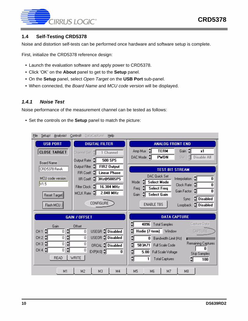
1.4 Self-Testing CRD5378Noise and distortion self-tests can be performed once hardware and software setup is complete.
First, initialize the CRD5378 reference design:
• Launch the evaluation software and apply power to CRD5378.• Click ‘OK’ on the About panel to get to the Setup panel.• On the Setup panel, select Open Target on the USB Port sub-panel.• When connected, the Board Name and MCU code version will be displayed.
1.4.1 Noise TestNoise performance of the measurement channel can be tested as follows:
• Set the controls on the Setup panel to match the picture:
10 DS639RD2
CRD5378
• Once the Setup panel is set, select Configure on the Digital Filter sub-panel.• After digital filter configuration is complete, click Capture on the Data Capture sub-panel.• Once the data record is collected, the Analysis panel is automatically displayed.• Select Noise FFT from the Test Select control to display the calculated noise statistics.• Verify the noise performance (S/N) is 124 dB or better.
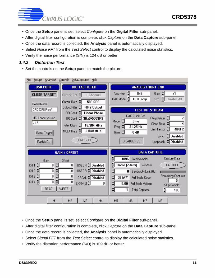
1.4.2 Distortion Test• Set the controls on the Setup panel to match the picture:
• Once the Setup panel is set, select Configure on the Digital Filter sub-panel.• After digital filter configuration is complete, click Capture on the Data Capture sub-panel.• Once the data record is collected, the Analysis panel is automatically displayed.• Select Signal FFT from the Test Select control to display the calculated noise statistics.• Verify the distortion performance (S/D) is 109 dB or better.
DS639RD2 11
CRD5378
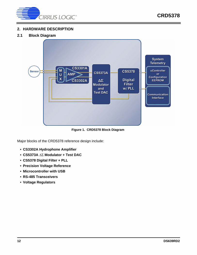
2. HARDWARE DESCRIPTION2.1 Block Diagram
Major blocks of the CRD5378 reference design include:
• CS3302A Hydrophone Amplifier • CS5373A ∆Σ Modulator + Test DAC• CS5378 Digital Filter + PLL• Precision Voltage Reference• Microcontroller with USB• RS-485 Transceivers• Voltage Regulators
Figure 1. CRD5378 Block Diagram
12 DS639RD2
CRD5378
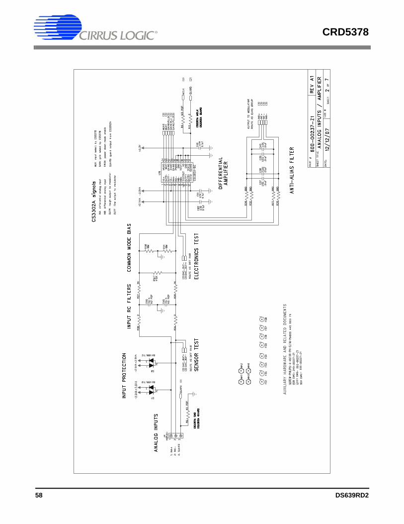
2.2 Analog Hardware2.2.1 Analog Inputs
2.2.1.1 External Inputs - INA
External signals into CRD5378 are from two major classes of sensors, moving coil geophones and piezo-electric hydrophones. Geophones are low-impedance sensors optimized to measure vibrations in landapplications. Hydrophones are high-impedance sensors optimized to measure pressure in marine appli-cations. Other sensors for earthquake monitoring and military applications are considered as geophonesfor this data sheet.
External signals connect to CRD5378 through a 3-pin header on the left side of the PCB. This headermakes a connection to the differential INA amplifier inputs and to either a GND or GUARD signal for con-nection to the sensor cable shields, if present.
2.2.1.2 GUARD Output, GND Connection
The CS3302A hydrophone amplifier provides a GUARD signal output on pin 13 designed to actively drivethe cable shield of a high impedance sensor with the common mode voltage of the sensor differential sig-nal. This GUARD output on the cable shield minimizes leakage by minimizing the voltage differential be-tween the sensor signal and the cable shield. The CS3301A geophone amplifier does not have a GUARDoutput. Instead, the CS3301A amplifier expects an MCLK clock input to pin 13, which is needed for itschopper stabilization circuitry. When using a CS3301A amplifier, a cable shield termination to GND is pro-vided for the sensor connection.
By default, CRD5378 uses the CS3302A amplifier. Therefore, the GUARD signal is connected to pin 3 ofthe input signal header, J4.
To configure CRD5378 with the CS3301A geophone amplifier, simply make the following three changes:
1) De-solder the 0 Ω resistor at R10 to remove the GUARD signal from pin 3 of J4.2) Populate R8 with a 0 Ω resistor to provide a cable shield termination to GND.3) Populate R9 with a 0 Ω resistor so that the CS3301A amplifier can receive its required master clock
(MCLK) from the CS5378 digital filter.
2.2.1.3 Internal Inputs - DAC_OUT, DAC_BUF
The CS5373A test DAC has two high performance differential test outputs, a precision output (DAC_OUT)and a buffered output (DAC_BUF). The DAC_OUT signal is wired directly to the INB inputs of theCS3302A amplifier for testing the performance of the electronics channel. The DAC_BUF signal is wiredto the INA inputs of the amplifier and is used to test the performance of the measurement channel with asensor attached.
Signal Input Pin HeaderCH1 INA J4
Table 6. Pin Header Input Connections
DS639RD2 13
CRD5378
2.2.1.4 Input Protection
Sensor inputs must have circuitry to protect the analog electronics from voltage spikes. Geophone coilsare susceptible to magnetic fields (especially from lightning) and hydrophones can produce large voltagespikes if located near an air gun source.
Discrete switching diodes quickly clamp the analog inputs to the power supply rails when the input voltagespikes. These diodes are reverse biased in normal operation and have low reverse bias leakage and ca-pacitance characteristics to maintain high linearity on the analog inputs.
2.2.1.5 Input RC Filters
Following the diode clamps is an RC filter network that bandwidth limits the sensor inputs into the ampli-fiers to 'chop-the-tops-off' residual voltage spikes not clamped by the discrete diodes. In addition, all Cir-rus Logic component ICs have built in ESD protection diodes guaranteed to 2000 V HBM / 200 V MM(JEDEC standard). The small physical size of these ESD diodes restricts their current capacity to 10 mA.
For land applications that use the CS3301A amplifier, the INA input has a common mode and differentialRC filter. The common mode filter sets a low-pass corner to shunt very high frequency components toground with minimal noise contribution. The differential filter sets a low-pass corner high enough not toaffect the magnitude response of the measurement bandwidth.
For marine applications that use the CS3302A amplifier, the inherent capacitance of the piezoelectric sen-sor is combined with large resistors to create an analog high-pass RC filter to eliminate the low-frequencycomponents of ocean noise.
Specification Value Dual Series Switching Diode - ON Semiconductor BAV99LT1 Surface Mount Package Type SOT-23 Non-Repetitive Peak Forward Current (1 µs, 1 ms, 1 s) 2.0 A, 1.0 A, 500 mA Reverse Bias Leakage (25 C to 85 C) 0.004 µA - 0.4 µA Reverse Bias Capacitance (0 V to 5 V) 1.5 pF - 0.54 pF
14 DS639RD2
CRD5378
2.2.1.6 Common Mode Bias
Differential analog signals into the CS3301A/02A amplifiers are required to be biased to the center of thepower supply voltage range, which for bipolar supplies is near ground potential. Resistors to create thecommon mode bias are selected based on the sensor impedance and may need to be modified from theCRD5378 defaults depending on the sensor to be used. Refer to the recommended operating bias con-ditions for the selected sensor, which are available from the sensor manufacturer.
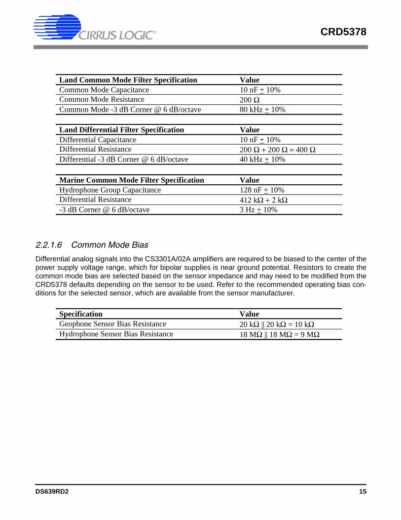
Land Common Mode Filter Specification Value Common Mode Capacitance 10 nF + 10% Common Mode Resistance 200 Ω Common Mode -3 dB Corner @ 6 dB/octave 80 kHz + 10% Land Differential Filter Specification Value Differential Capacitance 10 nF + 10% Differential Resistance 200 Ω + 200 Ω = 400 Ω Differential -3 dB Corner @ 6 dB/octave 40 kHz + 10%
Marine Common Mode Filter Specification Value Hydrophone Group Capacitance 128 nF + 10% Differential Resistance 412 kΩ + 2 kΩ -3 dB Corner @ 6 dB/octave 3 Hz + 10%
Specification Value Geophone Sensor Bias Resistance 20 kΩ || 20 kΩ = 10 kΩ Hydrophone Sensor Bias Resistance 18 MΩ || 18 MΩ = 9 MΩ
DS639RD2 15
CRD5378
2.2.2 Differential AmplifiersThe CS3301A/02A amplifiers act as a low-noise gain stage for internal or external differential analog sig-nals.
2.2.2.1 MCLK Input vs. GUARD Output
By default, CRD5378 uses the CS3302A hydrophone amplifier. The CS3302A amplifier is a very high in-put impedance device and achieves a 1/f noise performance typically buried below the low-frequencyocean noise. To minimize leakage from high impedance sensors connected to the CS3302A amplifier, pin13 produces a GUARD signal output to actively drive a sensor cable shield with the common mode volt-age of the sensor signal.
Comparing the CS3301A and CS3302A amplifiers, the functionality of pin 13 (MCLK input vs. GUARDoutput) is the only external difference. The CS3301A amplifier is chopper-stabilized requiring a clocksource on input pin 13. In order to run the chopper circuitry synchronous to the modulator analog samplingclock, the CS3301A amplifier pin 13 connects to the CS5378 digital filter (MCLK).
CRD5378 can be converted to use either the CS3301A and CS3302A amplifiers by installing the amplifierdevice and populating R8, R9, and R10 with 0 Ω resistors accordingly.
Replacement amplifiers can be requested as samples from the local Cirrus Logic sales representative.
2.2.2.2 Rough-Fine Outputs - OUTR, OUTF
The analog outputs of the CS3301A/02A differential amplifiers are split into rough charge and fine chargesignals for input to the CS5373A ∆Σ modulator.
Analog Signals Description INA Sensor analog input INB Test DAC analog input OUTR, OUTF Analog rough / fine outputs GUARD CS3302A guard output (R10 = 0 Ω, R9 = NO POP) Digital Signals Description MUX[0..1] Input mux selection GAIN[0..2] Gain range selection PWDN Power down mode enable CLK CS3301A clock input (R10 = NO POP, R9 = 0 Ω)
Amplifier CS3301A CS3302AU19 R8 + R9 *R10
Table 7. Amplifier Pin 13 Resistor Settings
16 DS639RD2
CRD5378
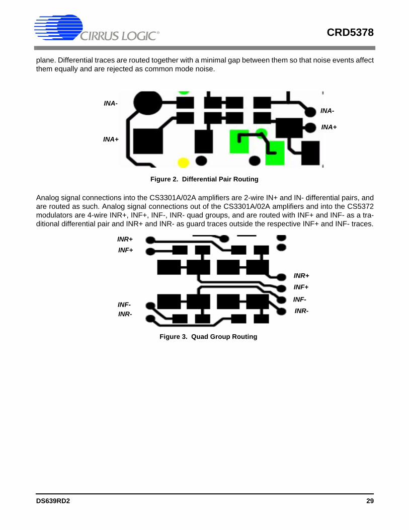
Analog signal traces out of the CS3301A/02A amplifiers and into the CS5373A modulator are 4-wireINR+, INF+, INF-, INR- quad groups, and are routed with INF+ and INF- as a traditional differential pairand INR+ and INR- as guard traces outside the respective INF+ and INF- traces.
2.2.2.3 Anti-alias RC Filters
The CS5373A ∆Σ modulator is 4th order and high frequency input signals can cause instability. Simplesingle-pole anti-alias RC filters are required between the CS3301A/02A amplifier outputs and theCS5373A modulator inputs to bandwidth limit analog signals into the modulator.
For the CRD5378, the CS3301A/02A amplifier outputs are connected to external 680 Ω series resistorsand a differential anti-alias RC filter is created by connecting 20 nF of high linearity differential capacitance(2x 10 nF C0G) between each half of the rough and fine signals.
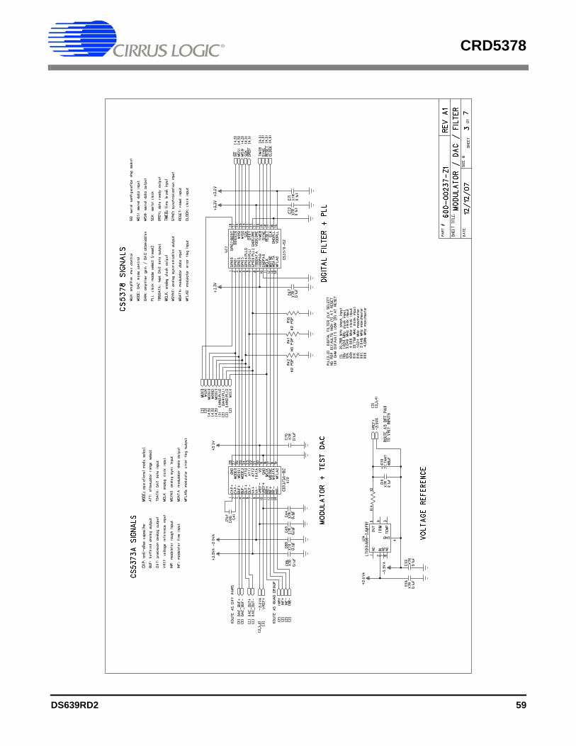
2.2.3 Delta-Sigma Modulator The CS5373A ∆Σ modulator performs the A/D function for differential analog signals from theCS3301A/02A amplifier. The digital output from the modulator is an oversampled ∆Σ bit stream.
2.2.3.1 Rough-Fine Inputs - INR, INF
The modulator analog inputs are separated into rough and fine signals, each of which has an anti-aliasRC filter to limit the signal bandwidth into the modulator inputs.
Analog Signals Description INR, INF Modulator analog rough / fine inputs VREF Voltage reference analog inputs Digital Signals Description MDATA Modulator delta-sigma data output MFLAG Modulator over-range flag output MCLK Modulator clock input MSYNC Modulator synchronization input
DS639RD2 17
CRD5378
2.2.4 Delta-Sigma Test DACThe CS5373A test DAC creates differential analog signals for system tests. Multiple test modes are avail-able and their use is described in the CS5373A data sheet.
2.2.4.1 Precision Output - DAC_OUT
The CS5373A test DAC has a precision output (DAC_OUT) that is routed directly to the amplifier INB in-puts. The input impedance of the CS3301A/02A INB amplifier inputs are high enough that the precisionoutput can be directly connected to the INB inputs.
2.2.4.2 Buffered Output - DAC_BUF
The CS5373A test DAC has a buffered output (DAC_BUF) that is routed to the amplifier INA inputs. Thisoutput is less sensitive to loading than the precision outputs, and can drive a sensor attached to the am-plifier INA inputs provided the sensor meets the impedance requirements specified in the CS5373A datasheet.
2.2.5 Voltage ReferenceA voltage reference on CRD5378 creates a precision voltage from the regulated analog supplies for themodulator and test DAC VREF inputs. Because the voltage reference output is generated relative to thenegative analog power supply, VREF+ is near GND potential for bipolar power supplies.
Analog Signals Description OUT Precision differential analog output BUF Buffered differential analog output CAP Capacitor connection for internal anti-alias filter VREF Voltage reference analog inputs Digital Signals Description TDATA Delta-sigma test data input MCLK Clock input SYNC Synchronization input MODE[0..2] Test mode selection ATT[0..2] Attenuation range selection
Specification Value Precision Reference - Linear Tech LT1019AIS8-2.5 Surface Mount Package Type SO-8 Output Voltage Tolerance +/- 0.05% Temperature Drift 10 ppm / degC Quiescent Current 0.65 mA Output Voltage Noise, 10 Hz - 1 kHz 4 ppmRMS Ripple Rejection, 10 Hz - 200 Hz > 100 dB
18 DS639RD2
CRD5378
2.2.5.1 VREF_MOD
The voltage reference output is provided to the CS5373A ∆Σ modulator and test DAC through a low-passRC filter. By filtering the voltage reference to the device, high-frequency noise is eliminated and any sig-nal-dependent sampling of VREF is isolated. The voltage reference signal is routed as a separate differ-ential pair from the large RC filter capacitor to control the sensitive VREF source-return currents and keepthem out of the ground plane. In addition to the RC filter function, the 68 uF filter capacitor provides a largecharge-well to help settle voltage reference sampling transients.
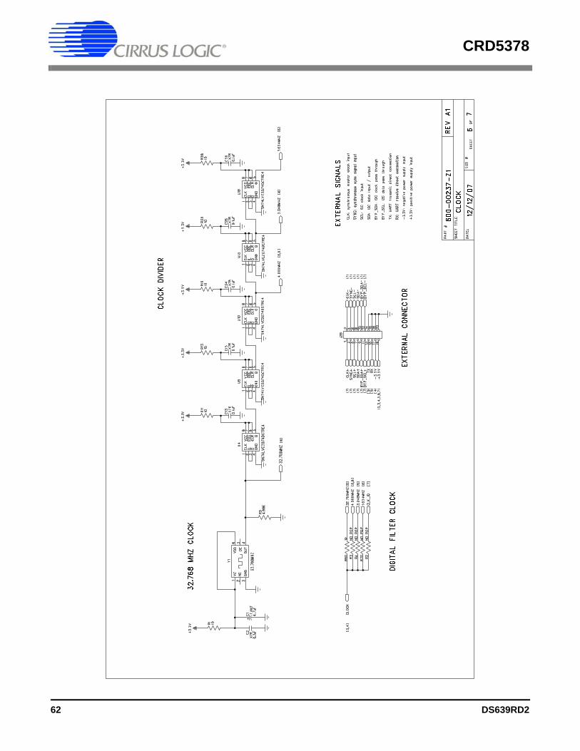
2.3 Digital Hardware2.3.1 Digital FilterThe CS5378 digital filter performs filtering and decimation of the ∆Σ bit stream from the CS5373A modu-lator. It also creates a ∆Σ bit stream output to create analog test signals in the CS5373A test DAC.
The CS5378 requires several control signal inputs from the external system.
Configuration and data collection are through the SPI port.
Modulator ∆Σ data is input through the modulator interface, and test DAC ∆Σ data is generated by the testbit stream generator.
Control Signals Description RESETz Reset input, active low BOOT Microcontroller / EEPROM boot mode select TIMEB Time Break input, rising edge triggered CLK Master clock input, 32.768 MHz SYNC Master synchronization input, rising edge triggered
SPI1 Signals Description DRDYz Data ready output, active low SCK Serial clock MISO Master in / slave out serial data MOSI Master out /slave in serial data SS: EECSz Serial chip select, active low
Modulator Signals Description MCLK Modulator clock output MSYNC Modulator synchronization output MDATA Modulator delta-sigma data input MFLAG Modulator over-range flag input TBSDATA Test DAC delta-sigma data output
DS639RD2 19
CRD5378
Amplifier, modulator and test DAC pin settings are controlled through the GPIO port.
2.3.1.1 Reset Options - BOOT, PLL
Immediately following the reset signal rising edge, the CS5378 digital filter latches the states of theGPIO[4..6]:PLL[0..2] and GPIO7:BOOT pins. The reset states of the GPIO[4..6]:PLL[0..2] pins select themaster clock input frequency and type, while the reset state of the GPIO7:BOOT pin selects how theCS5378 digital filter receives configuration data.
At reset, the CS5378 digital filter GPIO pins default as inputs with weak pull-up resistors enabled. There-fore, if left floating, the GPIO state will read high upon reset.
The CRD5378 provides the option to connect the GPIO[4..6]:PLL[0..2] and GPIO7:BOOT pins to 10k Ωpull-down resistors (R15, R41, and R42) so they will read low at reset. Because the pin states are latchedonly during reset, GPIO pins can be programmed and used normally after reset without affecting the PLLand BOOT selections.
Detailed information about the PLL input clock and BOOT mode selections at reset can be found in theCS5378 data sheet.
2.3.1.2 Configuration - SPI Port
On CRD5378, configuration of the digital filter is through the SPI port by the on-board 8051 microcontrol-ler, which receives commands from the PC evaluation software via the USB interface. Evaluation softwarecommands can write/read digital filter registers, specify digital filter coefficients and start/stop digital filteroperation.
By default the BOOT signal is set low to indicate configuration information is written by the microcontroller.
2.3.1.3 Phase Locked Loop
To make synchronous analog measurements throughout a distributed system, a synchronous systemclock needs to be provided to each measurement node. For evaluation testing purposes, the CRD5378can receive an external system clock by access through J1 and by non-population of R2, R3, R4, R60,and R70. With this external clock, a synchronous local clock can be created using the CS5378 PLL. The
GPIO Signals Description GPIO[0]:MUX[0] Amplifier input mux selection GPIO[1..3]:MODE[0..2] Test DAC mode selection GPIO[4..6]:GAIN[0..2] Amplifier gain / test DAC attenuation GPIO[7]:MUX[1] Amplifier input mux selection
20 DS639RD2
CRD5378
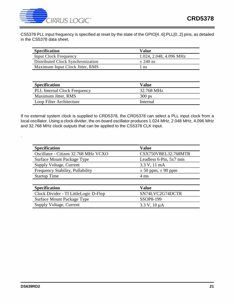
CS5378 PLL input frequency is specified at reset by the state of the GPIO[4..6]:PLL[0..2] pins, as detailedin the CS5378 data sheet.
If no external system clock is supplied to CRD5378, the CRD5378 can select a PLL input clock from alocal oscillator. Using a clock divider, the on-board oscillator produces 1.024 MHz, 2.048 MHz, 4.096 MHzand 32.768 MHz clock outputs that can be applied to the CS5378 CLK input.
.
Specification Value Input Clock Frequency 1.024, 2.048, 4.096 MHz Distributed Clock Synchronization ± 240 ns Maximum Input Clock Jitter, RMS 1 ns
Specification Value PLL Internal Clock Frequency 32.768 MHz Maximum Jitter, RMS 300 ps Loop Filter Architecture Internal
Specification Value Oscillator - Citizen 32.768 MHz VCXO CSX750VBEL32.768MTR Surface Mount Package Type Leadless 6-Pin, 5x7 mm Supply Voltage, Current 3.3 V, 11 mA Frequency Stability, Pullability ± 50 ppm, ± 90 ppm Startup Time 4 ms
Specification Value Clock Divider - TI LittleLogic D-Flop SN74LVC2G74DCTR Surface Mount Package Type SSOP8-199 Supply Voltage, Current 3.3 V, 10 µA
DS639RD2 21
CRD5378
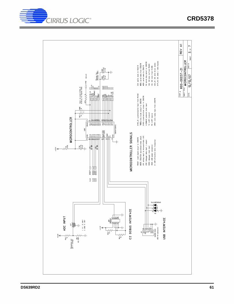
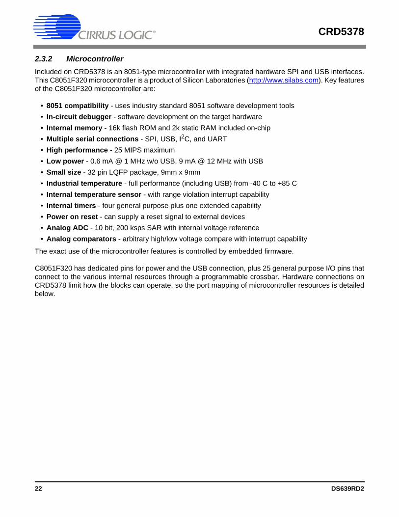
2.3.2 MicrocontrollerIncluded on CRD5378 is an 8051-type microcontroller with integrated hardware SPI and USB interfaces.This C8051F320 microcontroller is a product of Silicon Laboratories (http://www.silabs.com). Key featuresof the C8051F320 microcontroller are:
• 8051 compatibility - uses industry standard 8051 software development tools• In-circuit debugger - software development on the target hardware• Internal memory - 16k flash ROM and 2k static RAM included on-chip• Multiple serial connections - SPI, USB, I2C, and UART• High performance - 25 MIPS maximum• Low power - 0.6 mA @ 1 MHz w/o USB, 9 mA @ 12 MHz with USB• Small size - 32 pin LQFP package, 9mm x 9mm• Industrial temperature - full performance (including USB) from -40 C to +85 C• Internal temperature sensor - with range violation interrupt capability• Internal timers - four general purpose plus one extended capability• Power on reset - can supply a reset signal to external devices• Analog ADC - 10 bit, 200 ksps SAR with internal voltage reference• Analog comparators - arbitrary high/low voltage compare with interrupt capability
The exact use of the microcontroller features is controlled by embedded firmware.
C8051F320 has dedicated pins for power and the USB connection, plus 25 general purpose I/O pins thatconnect to the various internal resources through a programmable crossbar. Hardware connections onCRD5378 limit how the blocks can operate, so the port mapping of microcontroller resources is detailedbelow.
22 DS639RD2
CRD5378
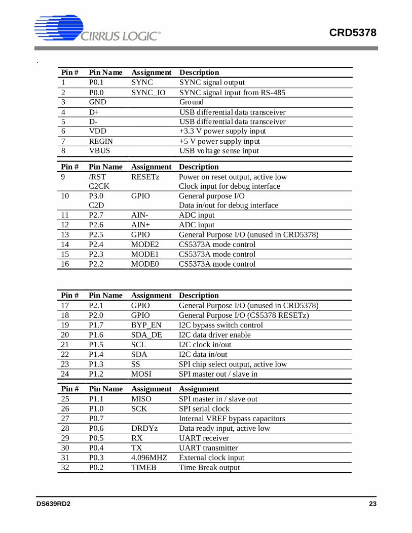
.Pin # Pin Name Assignment Description 1 P0.1 SYNC SYNC signal output 2 P0.0 SYNC_IO SYNC signal input from RS-485 3 GND Ground 4 D+ USB differential data transceiver 5 D- USB differential data transceiver 6 VDD +3.3 V power supply input 7 REGIN +5 V power supply input 8 VBUS USB voltage sense input
Pin # Pin Name Assignment Description 9 /RST
C2CK RESETz Power on reset output, active low
Clock input for debug interface 10 P3.0
C2D GPIO General purpose I/O
Data in/out for debug interface 11 P2.7 AIN- ADC input 12 P2.6 AIN+ ADC input 13 P2.5 GPIO General Purpose I/O (unused in CRD5378) 14 P2.4 MODE2 CS5373A mode control 15 P2.3 MODE1 CS5373A mode control 16 P2.2 MODE0 CS5373A mode control
Pin # Pin Name Assignment Description 17 P2.1 GPIO General Purpose I/O (unused in CRD5378) 18 P2.0 GPIO General Purpose I/O (CS5378 RESETz) 19 P1.7 BYP_EN I2C bypass switch control 20 P1.6 SDA_DE I2C data driver enable 21 P1.5 SCL I2C clock in/out 22 P1.4 SDA I2C data in/out 23 P1.3 SS SPI chip select output, active low 24 P1.2 MOSI SPI master out / slave in
Pin # Pin Name Assignment Assignment 25 P1.1 MISO SPI master in / slave out 26 P1.0 SCK SPI serial clock 27 P0.7 Internal VREF bypass capacitors 28 P0.6 DRDYz Data ready input, active low 29 P0.5 RX UART receiver 30 P0.4 TX UART transmitter 31 P0.3 4.096MHZ External clock input 32 P0.2 TIMEB Time Break output
DS639RD2 23
CRD5378
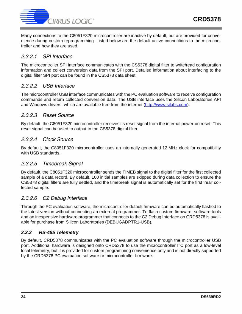
Many connections to the C8051F320 microcontroller are inactive by default, but are provided for conve-nience during custom reprogramming. Listed below are the default active connections to the microcon-troller and how they are used.
2.3.2.1 SPI Interface
The microcontroller SPI interface communicates with the CS5378 digital filter to write/read configurationinformation and collect conversion data from the SPI port. Detailed information about interfacing to thedigital filter SPI port can be found in the CS5378 data sheet.
2.3.2.2 USB Interface
The microcontroller USB interface communicates with the PC evaluation software to receive configurationcommands and return collected conversion data. The USB interface uses the Silicon Laboratories APIand Windows drivers, which are available free from the internet (http://www.silabs.com).
2.3.2.3 Reset Source
By default, the C8051F320 microcontroller receives its reset signal from the internal power-on reset. Thisreset signal can be used to output to the CS5378 digital filter.
2.3.2.4 Clock Source
By default, the C8051F320 microcontroller uses an internally generated 12 MHz clock for compatibilitywith USB standards.
2.3.2.5 Timebreak Signal
By default, the C8051F320 microcontroller sends the TIMEB signal to the digital filter for the first collectedsample of a data record. By default, 100 initial samples are skipped during data collection to ensure theCS5378 digital filters are fully settled, and the timebreak signal is automatically set for the first ‘real’ col-lected sample.
2.3.2.6 C2 Debug Interface
Through the PC evaluation software, the microcontroller default firmware can be automatically flashed tothe latest version without connecting an external programmer. To flash custom firmware, software toolsand an inexpensive hardware programmer that connects to the C2 Debug Interface on CRD5378 is avail-able for purchase from Silicon Laboratories (DEBUGADPTR1-USB).
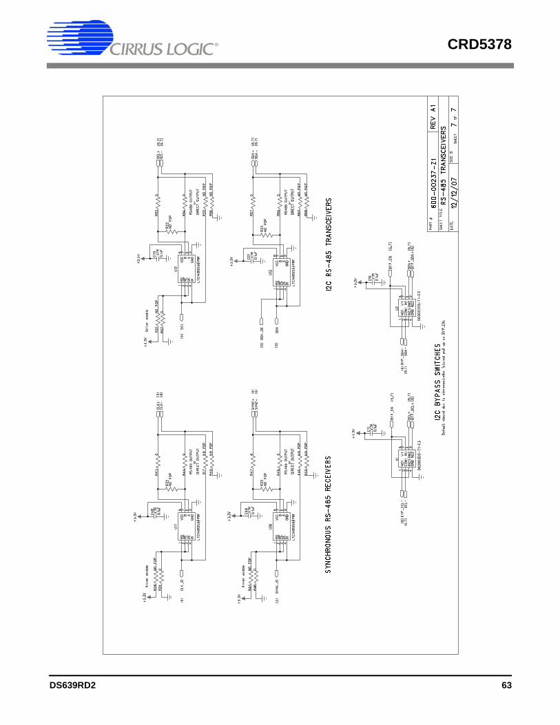
2.3.3 RS-485 TelemetryBy default, CRD5378 communicates with the PC evaluation software through the microcontroller USBport. Additional hardware is designed onto CRD5378 to use the microcontroller I2C port as a low-levellocal telemetry, but it is provided for custom programming convenience only and is not directly supportedby the CRD5378 PC evaluation software or microcontroller firmware.
24 DS639RD2
CRD5378
Telemetry signals enter CRD5378 through RS-485 transceivers, which are differential current modetransceivers that can reliably drive long distance communication. Data passes through the RS-485 trans-ceivers to the microcontroller I2C interface and the clock and synchronization inputs.
2.3.3.1 CLK, SYNC
Clock and synchronization telemetry signals into CRD5378 are received through RS-485 twisted pairs.These signals are required to be distributed through the external system with minimal jitter and timingskew, and so are normally driven through high-speed bus connections.
Synchronization of the measurement channel is critical to ensure simultaneous analog sampling acrossa network. Several options are available for connecting a SYNC signal through the RS-485 telemetry tothe digital filter.
A direct connection is made when the SYNC_IO signal is received over the dedicated RS-485 twisted pairand sent directly to the digital filter SYNC pin (with a 0 Ω resistor installed at R71). The incoming SYNC_IOsignal must be synchronized to the network at the transmitter since no local timing adjustment is available.
A microcontroller hardware connection is made when the SYNC_IO signal is received over the dedicatedRS-485 twisted pair and detected by a microcontroller interrupt. The microcontroller can then use an in-ternal counter to re-time the SYNC signal output to the digital filter SYNC input as required.
A microcontroller software connection is made when the SYNC signal output is created by the microcon-troller on command from the system telemetry. The microcontroller can use an internal counter to re-timethe SYNC signal output to the digital filter SYNC input as required.
Specification Value RS-485 Transceiver - Linear Tech LTC1480IS8 Surface Mount Package Type SOIC-8, 5mm x 6mm Supply Voltage, Quiescent Current 3.3V, 600 µA Maximum Data Rate 2.5 Mbps Transmitter Delay, Receiver Delay 25 - 80 ns, 30 - 200 ns Transmitter Current, Full Termination (60 Ω) 25 mA Transmitter Current, Half Termination (120 Ω) 13 mA
Specification Value Synchronous Inputs, 2 wires each CLK±, SYNC±
Specification Value Distributed SYNC Signal Synchronization ± 240 ns Distributed Clock Synchronization ± 240 ns Analog Sampling Synchronization Accuracy ± 480 ns
DS639RD2 25
CRD5378
2.3.3.2 I2C - SCL, SDA, Bypass
The I2C® telemetry connections to CRD5378 transmit and receive through RS-485 twisted pairs. Becausesignals passing through the transceivers are actively buffered, full I2C bus arbitration and error detectioncannot be used (i.e. high-impedance NACK).
The I2C inputs and outputs can be externally wired to create either a daisy chain or a bus type network,depending how the telemetry system is to be implemented. Analog switches included on CRD5378 canbypass the I2C signals to create a bus network from a daisy chain network following address assignment.
When CRD5378 is used in a distributed measurement network, each node must have a unique address.This address is used to transmit individual configuration commands and tag the source of returned con-version data. Address assignment can be either dynamic or static, depending how the telemetry systemis to be implemented.
Dynamic address assignment uses daisy-chained I2C connections to assign an address to each mea-surement node. Once a node receives an address, it enables the I2C bypass switches to the next nodeso it can be assigned an address.
Static address assignment has a serial number assigned to each node during manufacturing. Whenplaced in the network the location is recorded and a master list of serial numbers vs. location is main-tained. Alternately, a location dependent serial number can be assigned during installation.
2.3.4 UART ConnectionA UART connection on CRD5378 provides a low-speed standardized connection for telemetry solutionsnot using I2C. UART connections are provided for custom programming convenience only and are not di-rectly supported by the CRD5378 PC evaluation software or microcontroller firmware.
Specification Value I2C Inputs, 2 wires each SCL±, SDA± I2C Outputs, 2 wires each BYP_SCL±, BYP_SDA± I2C Bypass Switch Control BYP_EN
Specification Value UART Connections, 2 wires each TX/GND, RX/GND
26 DS639RD2
CRD5378
2.3.5 External ConnectorPower supplies and telemetry signals route to J26, a 20-pin double row connector with 0.1" spacing. Thisheader provides a compact standardized connection to the CRD5378 external signals.
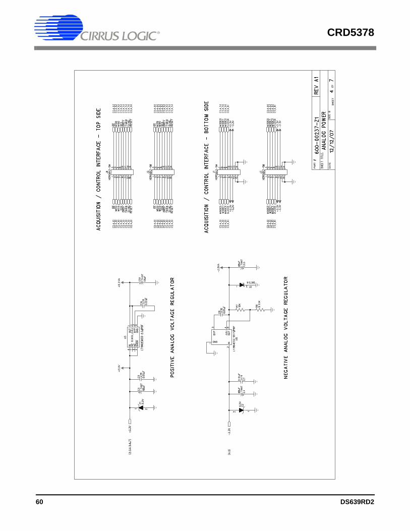
2.4 Power SuppliesPower is supplied to CRD5378 through the +3.3 V and -3.3 V voltage inputs on the external connector(J26), which are typically from an external AC-DC or DC-DC converter. Digital circuitry on CRD5378 isdriven directly from the +3.3 V input, while on-board linear regulators create +2.5 V and - 2.5 V analogpower supplies from +3.3 V and -3.3 V.
The +3.3 V and -3.3 V power supply inputs have zener protection diodes that limit the maximum input volt-ages to +5 V or -5 V with respect to ground. Each input also has 68 uF bulk capacitance for bypassingand to help settle transients and another 0.01 uF capacitor to bypass high frequency noise.
2.4.1 Analog Voltage RegulatorsLinear voltage regulators create the positive and negative analog power supply voltages to the analogcomponents on CRD5378. These regulate the +3.3 V and -3.3 V power supply inputs to create the +2.5 Vand -2.5 V analog power supplies.
Pins Name Signal 1, 2 CLK+, CLK- Clock Input 3, 4 SYNC+, SYNC- Synchronization Input 5, 6 SCL+, SCL- I2C Clock 7, 8 SDA+, SDA- I2C Data 9, 10 BYP_SDA+, BYP_SDA- I2C Data Bypass 11, 12 BYP_SCL+, BYP_SCL- I2C Clock Bypass 13, 14 TX, GND UART transmit 15, 16 RX, GND UART receive 17, 18 -3.3V, GND Negative Power Supply 19, 20 +3.3V, GND Positive Power Supply
Specification Value Positive Analog Power Supply +2.5 V Low Noise Micropower Regulator - Linear Tech LT1962ES8-2.5 Surface Mount Package Type MSOP-8 Load Regulation, -40 C to +85 C +/- 25 mV Quiescent Current, Current @ 100 mA Load 30 µA, 2 mA Output Voltage Noise, 10 Hz - 100 kHz 20 µVRMS Ripple Rejection, DC - 200 Hz > 60 dB
DS639RD2 27
CRD5378
The +2.5 V and -2.5 V power supplies to the analog components on CRD5378 include reverse biasedSchottky diodes to ground to protect against reverse voltages that could latch-up the CMOS analog com-ponents. Also included on +2.5 V and -2.5 V are 68 uF bulk capacitors for bypassing and to help settletransients plus individual 0.1 uF bypass capacitors local to the power supply pins of each device.
2.5 PCB Layout2.5.1 Layer StackCRD5378 layers 1 and 6 are dedicated as analog routing layers. All critical routes are on these two lay-ers. Some microcontroller digital routes are also included on these layers away from the analog signalroutes.
CRD5378 layer 2 is a solid ground plane without splits or routing. A solid ground plane provides the bestreturn path for bypassed noise to leave the system. No separate analog ground is required since analogsignals on CRD5378 are differentially routed.
CRD5378 layer 3 is dedicated for power supply routing. Each power supply net includes at least 68 µFbulk capacitance as a charge well for settling transient currents.
CRD5378 layer 4 is dedicated as a digital routing layer.
CRD5378 layer 5 is a solid ground plane without splits or routing. A solid ground plane provides the bestreturn path for bypassed noise to leave the system. No separate analog ground is required since analogsignals on CRD5378 are differentially routed.
2.5.2 Differential PairsAnalog signal routes on CRD5378 are differential with dedicated + and - traces. All source and return an-alog signal currents are constrained to the differential pair route and do not return through the ground
Specification Value Negative Analog Supply -2.5 V Low Noise Micropower Regulator - Linear Tech LT1964ES5-BYP Surface Mount Package Type SOT-23 Load Regulation, -40 C to +85 C +/- 30 mV Quiescent Current, Current @ 100 mA Load 30 µA, 1.3 mA Output Voltage Noise, 10 Hz - 100 kHz 20 µVRMS Ripple Rejection, DC - 200 Hz > 45 dB
28 DS639RD2
CRD5378
plane. Differential traces are routed together with a minimal gap between them so that noise events affectthem equally and are rejected as common mode noise.
Analog signal connections into the CS3301A/02A amplifiers are 2-wire IN+ and IN- differential pairs, andare routed as such. Analog signal connections out of the CS3301A/02A amplifiers and into the CS5372modulators are 4-wire INR+, INF+, INF-, INR- quad groups, and are routed with INF+ and INF- as a tra-ditional differential pair and INR+ and INR- as guard traces outside the respective INF+ and INF- traces.
Figure 2. Differential Pair Routing
INA-
INA+
INA-
INA+
Figure 3. Quad Group Routing
INR+INF+
INF-INR-
INR+INF+
INF-INR-
DS639RD2 29
CRD5378
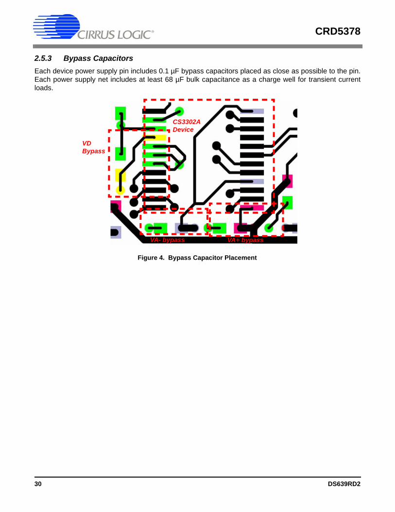
2.5.3 Bypass CapacitorsEach device power supply pin includes 0.1 µF bypass capacitors placed as close as possible to the pin.Each power supply net includes at least 68 µF bulk capacitance as a charge well for transient currentloads.
Figure 4. Bypass Capacitor Placement
VDBypass
CS3302ADevice
VA+ bypassVA- bypass
30 DS639RD2
CRD5378
3. SOFTWARE DESCRIPTION3.1 Menu Bar
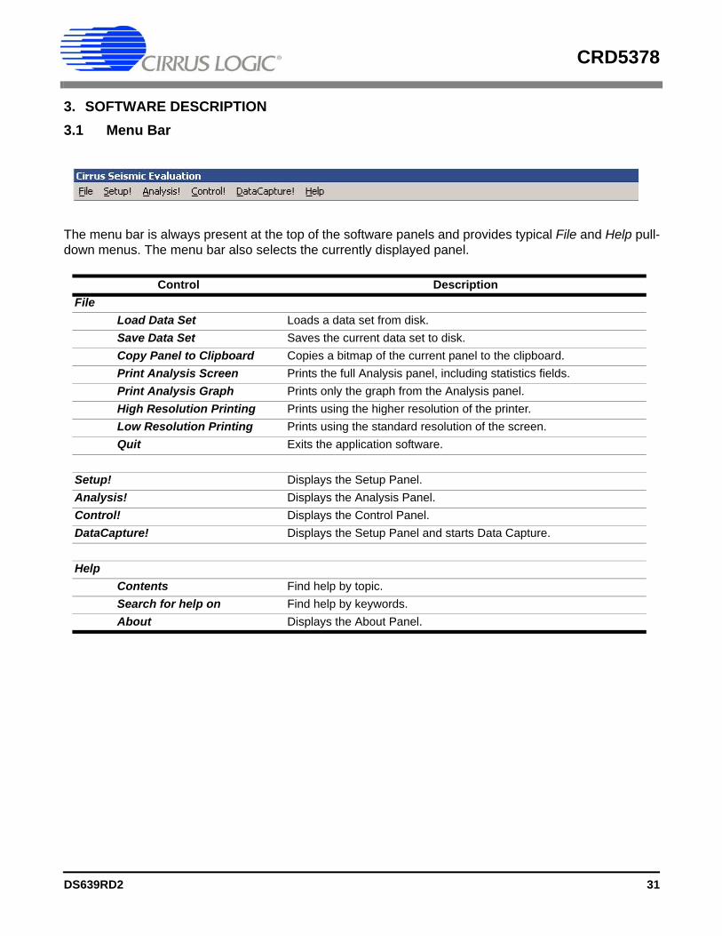
The menu bar is always present at the top of the software panels and provides typical File and Help pull-down menus. The menu bar also selects the currently displayed panel.
Control DescriptionFile
Load Data Set Loads a data set from disk.Save Data Set Saves the current data set to disk.Copy Panel to Clipboard Copies a bitmap of the current panel to the clipboard.Print Analysis Screen Prints the full Analysis panel, including statistics fields.Print Analysis Graph Prints only the graph from the Analysis panel.High Resolution Printing Prints using the higher resolution of the printer.Low Resolution Printing Prints using the standard resolution of the screen.Quit Exits the application software.
Setup! Displays the Setup Panel.Analysis! Displays the Analysis Panel.Control! Displays the Control Panel.DataCapture! Displays the Setup Panel and starts Data Capture.
HelpContents Find help by topic.Search for help on Find help by keywords.About Displays the About Panel.
DS639RD2 31
CRD5378
3.2 About Panel
The About panel displays copyright information for the Cirrus Seismic Evaluation software.
Click OK to exit this panel. Select Help About from the menu bar to display this panel.
32 DS639RD2
CRD5378
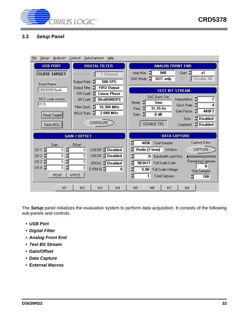
3.3 Setup Panel
The Setup panel initializes the evaluation system to perform data acquisition. It consists of the followingsub-panels and controls.
• USB Port• Digital Filter• Analog Front End• Test Bit Stream• Gain/Offset• Data Capture• External Macros
DS639RD2 33
CRD5378
3.3.1 USB PortThe USB Port sub-panel sets up the USB communication interface between the PC and the target board.
Control DescriptionOpen Target Open USB communication to the target board and read the board name and micro-
controller firmware version. When communication is established, the name of this control changes to ‘Close Target’ and Setup, Analysis and Control panel access becomes available in the menu bar.
Close Target Disconnects the previously established USB connection. On disconnection, this con-trol changes to ‘Open Target’ and the Setup, Analysis and Control panel access becomes unavailable in the menu bar. The evaluation software constantly monitors the USB connection status and automatically disconnects if the target board is turned off or the USB cable is unplugged.
Board Name Displays the type of target board currently connected.MCU code version Displays the version number of the microcontroller code on the connected target
board.Reset Target Sends a software reset command to the target board.Flash MCU Programs the microcontroller code on the target board using the .thx file found in the
“C:\Program Files\Cirrus Seismic Evaluation” directory. This feature permits repro-gramming of the microcontroller (without using a hardware programmer) when a new version of the MCU code becomes available.
34 DS639RD2
CRD5378
3.3.2 Digital FilterThe Digital Filter sub-panel sets up the digital filter configuration options.
By default the Digital Filter sub-panel configures the system to use on-chip coefficients and test bitstream data. The on-chip data can be overwritten by loading custom coefficients and test bit stream datafrom the Customize sub-panel on the Control panel.
Any changes made under this sub-panel will not be applied to the target board until the Configure buttonis pushed. The Configure button writes the new configuration to the target board and then enables thedata Capture button.
Control DescriptionChannel Set Selects the number of channels that are enabled in the digital filter. For the CS5378
digital filter, only 1 can be enabled.Output Rate Selects the output word rate of the digital filter. Output word rates from 4000 SPS to
1 SPS (0.25 mS to 1 S) are available.Output Filter Selects the output filter stage from the digital filter. Sinc output, FIR1 output, FIR2
output, IIR 1st order output, IIR 2nd order output, or IIR 3rd order output can be selected. FIR2 output provides full decimation of the modulator data.
FIR Coeff Selects the on-chip FIR coefficient set to use in the digital filter. Linear phase or min-imum phase FIR coefficients can be selected.
IIR Coeff Selects the on-chip IIR coefficient set to use in the digital filter. Coefficient sets pro-ducing a 3 Hz high-pass corner at 2000 SPS, 1000 SPS, 500 SPS, 333 SPS, and 250 SPS can be selected.
Filter Clock Sets the digital filter internal clock rate. Lower internal clock rates can save power when using slow output word rates.
MCLK Rate Sets the analog sample clock rate. The CS5373A modulator and test DAC typically run with MCLK set to 2.048 MHz.
Configure Writes all information from the Setup panel to the digital filter. The data Capture but-ton becomes available once the configuration information is written to the target board.
DS639RD2 35
CRD5378
3.3.3 Analog Front EndThe Analog Front End sub-panel configures the amplifier, modulator, and test DAC pin options. Pin op-tions are controlled through the GPIO outputs of the digital filter.
Any changes made under this sub-panel will not be applied to the target board until the Configure buttonis pushed. The Configure button writes the new configuration to the target board and then enables thedata Capture button.
3.3.4 Test Bit StreamThe Test Bit Stream sub-panel configures test bit stream (TBS) generator parameters. The digital filterdata sheet describes TBS operation and options.
The DAC Quick Set controls automatically set the Interpolation, Clock Rate, and Gain Factor controlsbased on the selected Mode, Freq, and Gain. Additional configurations can be programmed by writing theInterpolation, Clock Rate, and Gain Factor controls manually.
Any changes made under this sub-panel will not be applied to the target board until the Configure buttonis pushed. The Configure button writes the new configuration to the target board and then enables thedata Capture button.
Control DescriptionAmp Mux Selects the input source for the CS3301A/02A amplifiers. An internal termination,
external INA inputs or external INB inputs can be selected.DAC Mode Selects the operational mode of the CS5373A test DAC. The test DAC operational
modes are AC dual output (OUT&BUF), AC precision output (OUT only), AC buffered output (BUF only), DC common mode output (DC Common), DC differential output (DC Diff), or AC common mode output (AC Common). The test DAC can also be powered down (PWDN) when not in use to save power.
Gain Sets the amplifier gain range and test DAC attenuation. Amplifier gain and DAC attenuation settings of 1x, 2x, 4x, 8x, 16x, 32x, or 64x can be selected and are con-trolled together.
Sw Selects how the DAC_BUF to INA analog switches are enabled when connected to the CRD5376. This control is not applicable to the CRD5378 and is disabled.
Control DescriptionDAC Quick Set Automatically sets test bit stream options. Mode selects sine or impulse output mode,
Freq selects the test signal frequency for sine mode, and Gain selects the test signal amplitude in dB.
Interpolation Manual control for the data interpolation factor of the test bit stream generator.Clock Rate Manual control for the output clock and data rate of the test bit stream generator.Gain Factor Manual control to set the test bit stream signal amplitude.Sync Enables test bit stream synchronization by the MSYNC signal.Loopback Enables digital loopback from the test bit stream generator output to the digital filter
input.
36 DS639RD2
CRD5378
3.3.5 Gain/OffsetThe Gain / Offset sub-panel controls the digital filter GAIN and OFFSET registers for each channel.
The OFFSET and GAIN registers can be manually written with any 24-bit 2’s complement value from0x800000 to 0x7FFFFF. The USEGR, USEOR, ORCAL, and EXP[4:0] values enable gain correction, off-set correction, and offset calibration in the digital filter.
The offset calibration routine built into the digital filter is enabled by writing the ORCAL and EXP[4:0] bits.The EXP[4:0] value can range from 0x00 to 0x18 and represents an exponential shift of the calibrationfeedback, as described in the digital filter data sheet. Offset calibration results are automatically written tothe OFFSET registers and remain there, even after offset calibration is disabled.
Control DescriptionGain Displays the digital filter GAIN1 to GAIN4 registers.Offset Displays the digital filter OFFSET1 to OFFSET4 registers.Read Reads values from the GAIN and OFFSET registers.Write Writes values to the GAIN and OFFSET registers.USEGR Enables gain correction. When enabled, output samples are gained down by the
value in the GAIN register.(Output = GAIN / 0x7FFFFF).USEOR Enables offset correction. When enabled, output samples are offset by the value in
the OFFSET register. (Output = Sample - OFFSET).ORCAL Enables offset calibration using the exponent value from the EXP[4:0] control.
Results are automatically written to the OFFSET registers as they are calculated.EXP[4:0] Sets the exponential value used by offset calibration.
DS639RD2 37
CRD5378
3.3.6 Data CaptureThe Data Capture sub-panel collects samples from the target board and sets analysis parameters.
When the Capture button is pressed, the requested number of samples are collected from the target boardthrough the USB port. The maximum number of samples that can be collected is 1,048,576 (1M). Thenumber of samples per channel should be a power of two for the analysis FFT routines to work properly.
After data is collected, analysis is performed using the selected parameters and the results are displayedon the Analysis panel. The selected analysis window, bandwidth limit, full scale code, and full scale volt-age parameters can be modified for the data set currently in memory and the analysis re-run by pressingthe REFRESH button on the Analysis Panel.
Control DescriptionTotal Samples Sets the total number of samples to be collected. Multichannel acquisitions split the
requested number of samples among the channels. A maximum of 1,048,576 (1M) samples can be collected.
Window Selects the type of analysis windowing function to be applied to the collected data set. Used to ensure proper analysis of discontinuous data sets.
Bandwidth Limit (Hz) Sets the frequency range over which to perform analysis, used to exclude higher-fre-quency components. Default value of zero performs analysis for the full Nyquist fre-quency range.
Full Scale Code Defines the maximum positive full-scale 24-bit code from the digital filter. Used during FFT noise analysis to set the 0 dB reference level.
Full Scale Voltage Defines the maximum peak-to-peak input voltage for the nV/√Hz Spot Noise analy-sis.
Total Captures Sets the number of data sets to be collected and averaged together in the FFT mag-nitude domain. The maximum number of data sets that can be averaged is 100.
Capture Starts data collection from the target board through the USB port. After data collec-tion, analysis is run using parameters from this sub-panel.
Remaining Captures Indicates how many more data captures are remaining to complete the requested number of Total Captures. A zero value means that the current data capture is the last one.
Skip Samples Sets the total number of samples to be skipped prior to data collection. A maximum of 64K samples can be skipped
38 DS639RD2
CRD5378
3.3.7 External MacrosMacros are generated within the Macros sub-panel on the Control panel. Once a macro has been builtit can either be saved with a unique macro name to be run within the Macros sub-panel, or saved as anexternal macro and be associated with one of the External Macro buttons.
A macro is saved as an External Macro by saving it in the . /macros/ subdirectory using the name‘m1.mac’, ‘m2.mac’, etc. Depending on the selected name the macro will be associated with the corre-sponding External Macro button M1, M2, etc.
• M1 = . /macros/m1.mac• M2 = . /macros/m2.mac• etc.
External Macro buttons can be re-named on the panel by right clicking on them. The button name willchange, but the macro associated with that button is always saved as ‘m1.mac’, ‘m2.mac’, etc., in the. /macros/ subdirectory. The External Macro button names are stored in the file ‘Mnames.txt’, also in the. /macros/ subdirectory.
External Macros allow up to eight macros to be accessed quickly without having to load them into the Mac-ros sub-panel on the Control panel. These External Macros operate independently of the Macros sub-panel and are not affected by operations within it, except when a macro is saved to the . /macros/ subdi-rectory to replace a currently existing External Macro.
Control DescriptionM1 - M8 Runs the External Macro associated with that button.
DS639RD2 39
CRD5378
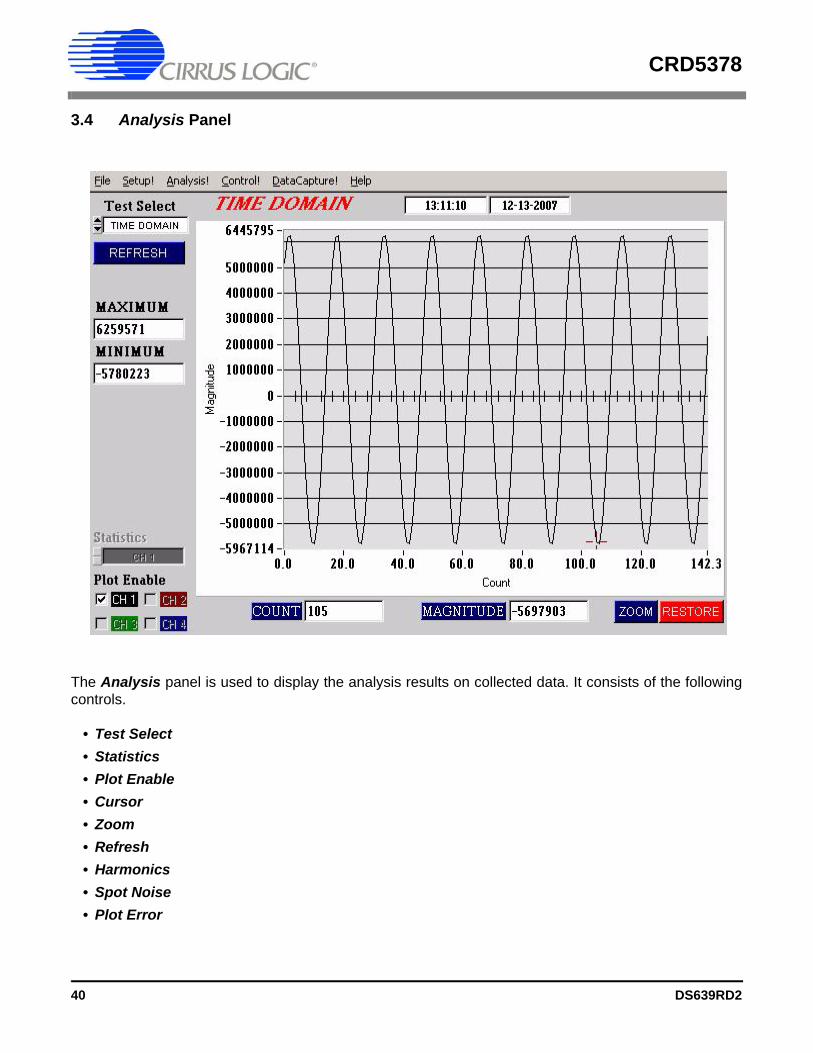
3.4 Analysis Panel
The Analysis panel is used to display the analysis results on collected data. It consists of the followingcontrols.
• Test Select• Statistics• Plot Enable• Cursor• Zoom• Refresh• Harmonics• Spot Noise• Plot Error
40 DS639RD2
CRD5378
3.4.1 Test SelectThe Test Select control sets the type of analysis to be run on the collected data set.
Control DescriptionTime Domain Runs a min / max calculation on the collected data set and then plots sample data
value vs. sample number.Histogram Runs a histogram calculation on the collected data set and then plots sample occur-
rence vs. sample value. Only valid for noise data since sine wave data varies over too many codes to plot as a histogram.
Signal FFT Runs an FFT on the collected data set and then plots frequency magnitude vs. fre-quency. Statistics are calculated using the largest frequency bin as a full-scale signal reference.
Noise FFT Runs an FFT on the collected data set and then plots frequency magnitude vs. fre-quency. Statistics are calculated using a simulated full-scale signal as a full-scale sig-nal reference.
DS639RD2 41
CRD5378
3.4.2 StatisticsThe Statistics control displays calculated statistics for the selected analysis channel. For multichanneldata captures, only one channel of calculated statistics are displayed at a time and is selected using theStatistics channel control.
Errors that affect statistical calculations will cause the Plot Error control to appear. Information about er-rors on specific channels can be accessed by enabling the plot of the channel using the Plot Enable con-trol and then accessing the Plot Error controls.
3.4.3 CursorThe Cursor control is used to identify a point on the graph using the mouse and then display its plot values.When any point within the plot area of the graph is clicked, the Cursor will snap to the closest plotted pointand the plot values for that point display below the graph.
Control DescriptionTime Domain
Max Maximum code of collected data set.Min Minimum code of collected data set.
HistogramMax Maximum code of collected data set.Min Minimum code of collected data set.Mean Mean of collected data set.Std Dev Standard Deviation of collected data set.Variance Variance of collected data set.
Signal FFTS/N Signal to Noise of calculated FFT.S/PN Signal to Peak Noise of calculated FFT.S/D Signal to Distortion of calculated FFT.S/N+D Signal to Noise plus Distortion of calculated FFT.# of bins Number of Bins covering the Nyquist frequency.
Noise FFTS/N Signal to Noise of calculated FFT.S/PN Signal to Peak Noise of calculated FFT.Spot Noise dB Spot Noise in dB/√Hz of calculated FFT.Spot Noise nV Spot Noise in nV/√Hz of calculated FFT.# of bins Number of Bins covering the Nyquist frequency.
42 DS639RD2
CRD5378
When using the Zoom function, the Cursor is used to select the corners of the area to zoom.
3.4.4 ZoomThe ZOOM function allows an area on the graph to be expanded.
To use the zoom function, click the ZOOM button and select the box corners of the area on the graph toexpand. The graph will then expand to show the details of this area, and the plot axes will be re-scaled.While zoomed, you can zoom in farther by repeating the process.
To restore the graph to its original scale, click the RESTORE button that appears while zoomed. If multiplezooms have been initiated, the RESTORE button will return to the previously viewed plot scale. RepeatedRESTORE will eventually return to the original plot scale. From within multiple zooms the original scalecan be directly restored by clicking the REFRESH button.
3.4.5 RefreshThe REFRESH button will clear and re-plot the current data set. Refresh can be used to apply new anal-ysis parameters from the Data Capture sub-panel, or to restore a ZOOM graph to its default plot scale.
3.4.6 HarmonicsThe HARMONICS control is only visible during a Signal FFT analysis and highlights the fundamental andharmonic bins used to calculate the Signal FFT statistics. HARMONICS highlighting helps to understandthe source of any Signal FFT plot errors.
3.4.7 Spot NoiseThe Spot Noise control (labeled dB or nV) is only visible during a Noise FFT analysis and selects the unitsused for plotting the graph, either dB/√Hz or nV/√Hz. The dB/Hz plot applies the Full Scale Code valuefrom the Data Capture sub-panel on the Setup panel to determine the 0 dB point of the dB axis. ThenV/√Hz plot applies the Full Scale Voltage value from the Data Capture sub-panel on the Setup panel todetermine the absolute scaling of the nV axis.
3.4.8 Plot ErrorThe PLOT ERROR control provides information about errors that occurred during an analysis. Analysiserrors are only reported if the channel that has the error is currently plotted.
An analysis error stores an error code in the numerical display box of the PLOT ERROR control. If morethan one error occurs, all error codes are stored and the last error code is displayed. Any of the accumu-lated error codes can be displayed by clicking on the numerical box and selecting it.
Once an error code is displayed in the numerical box, a description can be displayed by clicking the PLOTERROR button. This causes a dialog box to display showing the error number, the error channel, and atext error message.
DS639RD2 43
CRD5378
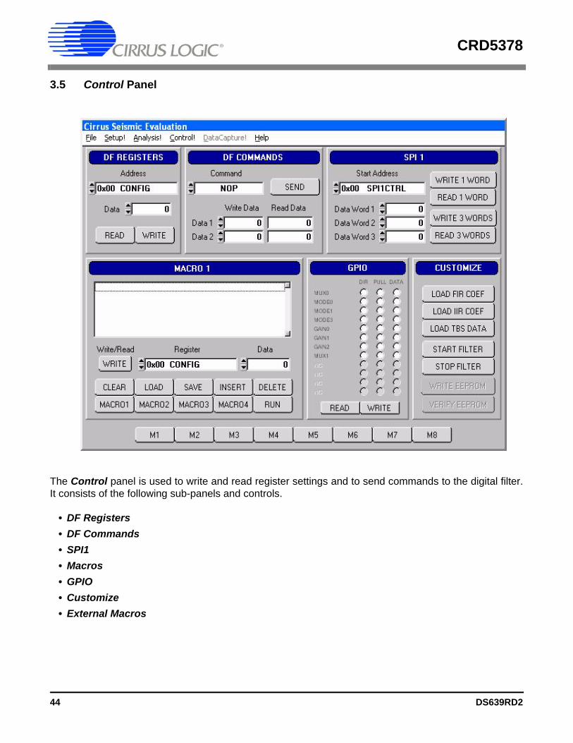
3.5 Control Panel
The Control panel is used to write and read register settings and to send commands to the digital filter.It consists of the following sub-panels and controls.
• DF Registers• DF Commands• SPI1• Macros• GPIO• Customize• External Macros
44 DS639RD2
CRD5378
3.5.1 DF RegistersThe DF Registers sub-panel writes and reads registers within the digital filter. Digital filter registers con-trol operation of the digital filter and the included hardware peripherals, as described in the digital filterdata sheet.
3.5.2 DF CommandsThe DF Commands sub-panel sends commands to the digital filter. The digital filter commands and theirrequired parameters are described in the digital filter data sheet.
Not all commands require write data values, and not all commands will return read data values. Somecommands require formatted data files for uploading custom coefficients or test bit stream data Exampleformatted data files are included in the SPI sub-directory of the software installation.
3.5.3 SPIThe SPI sub-panel writes and reads registers in the digital filter SPI register space. They can be used tocheck the SPI serial port status bits or to manually write commands to the digital filter.
Control DescriptionAddress Selects a digital filter register.Data Contains the data written to or read from the register.Read Initiates a register read.Write Initiates a register write.
Control DescriptionCommand Selects the command to be written to the digital filter.Write Data 1 Contains the SPI1DAT1 data to be written to the digital filter.Write Data 2 Contains the SPI1DAT2 data to be written to the digital filter.Read Data 1 Contains the SPI1DAT1 data read from the digital filter.Read Data 2 Contains the SPI1DAT2 data read from the digital filter.Send Initiates the digital filter command.
Control DescriptionStart Address Selects the address to begin the SPI transaction.Data Word 1 Contains the first data word written to or read from the SPI registers.Data Word 2 Contains the second data word written to or read from the SPI registers.Data Word 3 Contains the third data word written to or read from the SPI registers.Read 1 Word Initiates a 1 word SPI read transaction.Read 3 Words Initiates a 3 word SPI read transaction.Write 1 Word Initiates a 1 word SPI write transaction.Write 3 Words Initiates a 3 word SPI write transaction.
DS639RD2 45

CRD5378
3.5.4 MacrosThe Macros sub-panel is designed to write a large number of registers with a single command. This al-lows the target evaluation system to be quickly set into a specific state for testing.
The Register control gives access to both digital filter registers and SPI1 registers. These registers canbe written with data from the Data control, or data can be read and output to a text window. The Registercontrol can also select special commands to be executed, with the Data control used to define a param-eter value for the special command, if necessary.
3.5.5 GPIOThe GPIO sub-panel controls the digital filter GPIO pin configurations. GPIO pins have dedicated func-tions on the target board, but can be used in any manner for custom designs.
Control DescriptionWrite / Read Selects the type of operation to be performed by the inserted macro command.Register Selects the target register for the inserted macro command. Also selects special
commands that can be performed.Data Sets the register data value for the inserted macro command. Also sets the parame-
ter value for special commands.Clear Clears the currently displayed macro.Load Loads a previously saved macro.Save Saves the currently displayed macro. Macros can be saved with unique names or
can be saved as External Macros.Insert Inserts a macro command at the selected macro line. The macro command is built
from the Write/Read, Register, and Data controls.Delete Deletes the macro command at the selected macro line.Macro1 - Macro4 Selects which of the four working macros is displayed.Run Runs the currently displayed working macro.
Control DescriptionDirection Sets the selected GPIO pin as an output (*) or input ( ).Pull Up Turns the pull up resistor for the selected GPIO pin on (*) or off ( ).Data Sets the selected output GPIO pin to a high (*) or low ( ) level.Write Initiates a write to GPIO registers.The Direction, Pull Up and Data controls are read
to determine the register values to be written.Read Initiates a read from GPIO registers.The Direction, Pull Up and Data controls are
updated based on the register values that are read.
46 DS639RD2
CRD5378
3.5.6 CustomizeThe Customize sub-panel sends commands to upload custom FIR and IIR filter coefficients, upload cus-tom test bit stream data, start the digital filter, stop the digital filter, and write/read custom EEPROM con-figuration files to the on-board boot EEPROM. Example data files are included in a sub-directory of thesoftware installation.
3.5.7 External MacrosMacros are generated within the Macros sub-panel on the Control panel. Once a macro has been builtit can either be saved with a unique macro name to be run within the Macros sub-panel, or saved as anexternal macro and be associated with one of the External Macro buttons.
A macro is saved as an External Macro by saving it in the . /macros/ subdirectory using the name‘m1.mac’, ‘m2.mac’, etc. Depending on the selected name the macro will be associated with the corre-sponding External Macro button M1, M2, etc.
• M1 = . /macros/m1.mac• M2 = . /macros/m2.mac• etc.
External Macro buttons can be re-named on the panel by right clicking on them. The button name willchange, but the macro associated with that button is always saved as ‘m1.mac’, ‘m2.mac’, etc., in the. /macros/ subdirectory. The External Macro button names are stored in the file ‘Mnames.txt’, also in the. /macros/ subdirectory.
External Macros allow up to eight macros to be accessed quickly without having to load them into the Mac-ros sub-panel on the Control panel. These External Macros operate independently of the Macros sub-panel and are not affected by operations within it, except when a macro is saved to the . /macros/ subdi-rectory to replace a currently existing External Macro.
Control DescriptionLoad FIR Coef Write a set of FIR coefficients into the digital filter from a file.Load IIR Coef Write a set of IIR coefficients into the digital filter from a file.Load TBS Data Write a set of test bit stream data into the digital filter from a file.Start Filter Enables the digital filter by sending the Start Filter command.Stop Filter Disables the digital filter by sending the Stop Filter command.
Control DescriptionM1 - M8 Runs the External Macro associated with that button.
DS639RD2 47
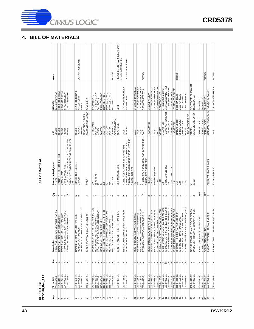
CRD5378
4. BILL OF MATERIALS C
IRR
US
LOG
ICC
RD
5378
_Rev
_A1.
PLB
ILL
OF
MA
TER
IAL
Item
Cirr
us P
/NR
evD
escr
iptio
nQ
tyR
efer
ence
Des
igna
tor
MFG
MFG
P/N
Not
es1
004-
0006
8-Z1
AC
AP
4.7
uF ±
10%
10V
NP
b TA
NT
CA
SE
A2
C1
C59
KE
ME
TT4
91A
475K
010A
S2
001-
0434
5-Z1
AC
AP
0.1
uF ±
10%
50V
X7R
NP
b 08
057
C2
C11
C12
C31
C48
C60
C78
KE
ME
TC
0805
C10
4K5R
AC
300
1-01
997-
Z1A
CA
P 0
.01u
F ±1
0% 2
5V X
7R N
Pb
0603
4C
3 C
6 C
7 C
14K
EM
ET
C06
03C
103K
3RA
C4
004-
0009
2-Z1
AC
AP
68u
F ±1
0% 1
0V T
AN
T N
Pb
CA
SE
C5
C4
C5
C20
C51
C53
KE
ME
TT4
91C
686K
010A
T5
001-
0219
4-Z1
AC
AP
0.1
uF ±
10%
25V
X7R
NP
b 06
0321
C13
C15
C16
C24
C25
C26
C30
C33
C36
C44
C
45 C
49 C
61 C
62 C
65 C
66 C
67 C
68 C
70 C
71
C72
KE
ME
TC
0603
C10
4K3R
AC
600
1-06
603-
Z1A
CA
P 0
.01u
F ±5
% 2
5V C
0G N
Pb
1206
5C
37 C
38 C
39 C
40 C
41K
EM
ET
C12
06C
103J
3GA
C7
000-
0000
8-Z1
AN
O P
OP
CA
P N
Pb
0805
0C
46 C
50N
O P
OP
NP
-CA
P-0
805
DO
NO
T P
OP
ULA
TE8
070-
0001
0-Z1
AD
IOD
E S
CH
TKY
BA
R 3
0V 0
.2A
NP
b S
OT2
31
D1
PH
ILIP
S
SE
MIC
ON
DU
CTO
RS
BA
T54
907
0-00
024-
Z1A
DIO
DE
SW
T 70
V 2
15m
A N
Pb
SO
T-23
2D
7 D
8O
N S
EM
ICO
ND
UC
TOR
BA
V99
LT1G
1007
0-00
055-
Z1A
DIO
DE
AR
RA
Y 5
V (T
VS
) ES
D N
Pb
SO
T143
1D
9LI
TTE
LFU
SE
SP
0503
BA
HTG
1111
5-00
221-
Z1A
HD
R 8
X2
ML
.050
" ST
GLD
NP
b S
M4
J1 J
2 J5
J6
SA
MTE
CFT
S-1
08-0
1-L-
DV
1211
0-00
263-
Z1A
CO
N U
SB
RC
PT
RA
5P
OS
MIN
I-B N
Pb
TH1
J3M
OLE
X54
819-
0519
1311
5-00
054-
Z1A
HD
R 3
x1 M
L .1
"CTR
S G
LD N
Pb
1J4
SA
MTE
CTS
W-1
03-2
6-G
-S14
115-
0001
1-Z1
AH
DR
10x
2 M
L .1
" 062
BD
ST
GLD
NP
b TH
1J2
6S
AM
TEC
TSW
-110
-07-
G-D
1511
5-00
013-
Z1A
HD
R 2
x2 M
L .1
"CTR
.062
BD
S G
LD N
Pb
1J5
7S
AM
TEC
TSW
-102
-07-
G-D
1611
5-00
003-
Z1A
HD
R 5
x2 M
L .1
"CTR
S G
LD N
Pb
1J6
0S
AM
TEC
TSW
-105
-07-
G-D
1708
0-00
004-
Z1A
WIR
E J
UM
PE
R 2
P 0
.1" B
RA
SS
NP
b TH
0JP
1 JP
2C
OM
PO
NE
NTS
C
OR
PO
RA
TIO
NTP
-101
-10
NO
PO
P
1830
4-00
004-
Z1A
SP
CR
STA
ND
OFF
4-4
0 TH
R N
Pb
.500
"L4
MH
1 M
H2
MH
5 M
H6
KE
YS
TON
E22
03R
EQ
UIR
ES
SC
RE
W 4
-40X
5X16
" PH
S
TEE
L, 3
00-0
0001
-01
1902
0-00
788-
Z1A
RE
S 1
0 O
HM
1/1
0W ±
1% N
Pb
0603
FIL
M9
R1
R11
R13
R14
R16
R25
R26
R60
R68
DA
LEC
RC
W06
0310
R0F
KE
A20
000-
0000
2-Z1
AN
O P
OP
RE
S N
Pb
0603
0R
2 R
3 R
4 R
8 R
9 R
15 R
17 R
22 R
23 R
32 R
33
R39
R40
R41
R42
R45
R49
R50
R51
R55
R56
R
61 R
63 R
69 R
70
NO
PO
PN
P-R
ES
-060
3D
O N
OT
PO
PU
LATE
2102
0-01
095-
Z1A
RE
S 4
.99k
OH
M 1
/10W
±1%
NP
b 06
031
R5
DA
LEC
RC
W06
034K
99FK
EA
2202
0-01
128-
Z1A
RE
S 9
.53k
OH
M 1
/10W
±1%
NP
b 06
031
R6
DA
LEC
RC
W06
039K
53FK
EA
2302
0-01
130-
Z1A
RE
S 1
0k O
HM
1/1
0W ±
1% N
Pb
0603
FIL
M1
R7
DA
LEC
RC
W06
0310
K0F
KE
A24
020-
0067
3-Z1
AR
ES
0 O
HM
1/1
0W ±
5% N
Pb
0603
FIL
M16
R10
R24
R34
R36
R43
R44
R46
R47
R48
R52
R
53 R
54 R
57 R
59 R
62 R
71D
ALE
CR
CW
0603
000Z
0EA
EC
O55
4
2502
1-01
391-
Z1A
RE
S 1
8M O
HM
1/8
W ±
5% N
Pb
0805
2R
31 R
38P
AN
AS
ON
ICE
RJ6
GE
YK
186V
2602
0-01
048-
Z1A
RE
S 2
k O
HM
1/1
0W ±
1% N
Pb
0603
FIL
M2
R35
R37
DA
LEC
RC
W06
032K
00FK
EA
2702
0-01
016-
Z1A
RE
S 1
k O
HM
1/1
0W ±
1% N
Pb
0603
FIL
M4
R64
R65
R66
R67
DA
LEC
RC
W06
031K
00FK
EA
2802
0-06
253-
Z1A
RE
S 4
12k
OH
M 1
/4W
±1%
NP
b 12
061
R14
7D
ALE
CR
CW
1206
412K
FKE
A29
060-
0019
5-Z1
AIC
LO
W V
DU
L S
PS
T A
NA
SW
NP
b M
SP
82
U1
U2
VIS
HA
YD
G20
03D
Q-T
1-E
330
060-
0016
3-Z1
AIC
LN
R 3
00m
A L
SE
LD
O R
EG
NP
b M
SO
P8
1U
3LI
NE
AR
TE
CH
LT19
62E
MS
8-2.
5#P
BF
3106
1-00
062-
Z1A
IC L
OG
SG
L D
-FF
CLR
PR
ES
T N
Pb
SS
OP
85
U4
U9
U10
U15
U16
TEX
AS
INS
TRU
ME
NTS
SN
74LV
C2G
74D
CTR
E4
3206
0-00
063-
Z1A
IC L
NR
V R
EG
200m
A N
EG
AD
J N
PbS
OT2
3-5
1U
5LI
NE
AR
TE
CH
LT19
64E
S5-
BY
P#P
BF
3306
0-00
162-
Z1A
IC 3
.3V
U L
W P
WR
RS
485
XC
VR
NP
SO
IC8
4U
12 U
13 U
17 U
18LI
NE
AR
TE
CH
LTC
1480
IS8#
PB
F34
060-
0023
6-Z1
AIC
LN
R P
RC
VR
F 2.
5V T
C10
NP
bSO
8-15
01
U14
LIN
EA
R T
EC
HLT
1019
AIS
8-2.
5#P
BF
3506
5-00
229-
Z2G
IC C
RU
S H
I-Z D
IDO
AM
P N
Pb
SS
OP
241
U19
CIR
RU
S L
OG
ICC
S33
02A
-ISZ/
GE
CO
554
3606
5-00
196-
Z1A
IC C
RU
S T
ES
T D
AC
NP
b S
SO
P28
1U
20C
IRR
US
LO
GIC
CS
5373
A-IS
Z/A
3706
5-00
130-
Z1A
IC C
RU
S 1
CH
DIG
FLT
R N
Pb
SS
OP
281
U22
CIR
RU
S L
OG
ICC
S53
78-IS
Z/A
3806
2-00
079-
Z1A
IC P
GM
US
B 1
6kB
FLA
S M
CU
NP
b LQ
FP32
1U
28S
ILIC
ON
LA
BO
RA
TOR
IES
INC
C80
51F3
20-G
Q
3910
2-00
017-
Z2A
OS
C 3
2.76
8MH
z 90
ppm
3.3
V V
CL
NP
b S
M1
Y1
CIT
IZE
NC
SX
750V
BE
L32.
768M
-UT
4007
0-00
053-
Z1A
DIO
DE
ZE
N T
R S
UP
5V
600
W P
K N
Pb
SM
2Z1
Z2
ON
SE
MIC
ON
DU
CTO
R1S
MB
5.0A
T3G
4160
3-00
237-
Z1A
AS
SY
DW
G P
WA
CR
D53
78-Z
NP
bR
EF
CIR
RU
S L
OG
IC60
3-00
237-
Z142
240-
0023
7-Z1
AP
CB
CR
D53
78-Z
NP
b1
CIR
RU
S L
OG
IC24
0-00
237-
Z143
600-
0023
7-Z1
A1
SC
HE
M C
RD
5378
-Z N
Pb
RE
FC
IRR
US
LO
GIC
600-
0023
7-Z1
EC
O55
444
300-
0002
5-Z1
AS
CR
EW
4-4
0X5/
16" P
H M
AC
H S
S N
Pb
4X
MH
1 X
MH
2 X
MH
5 X
MH
6B
UIL
DIN
G F
AS
TEN
ER
SP
MS
SS
440
003
1 P
H
4502
0-06
288-
Z1A
RE
S 6
80 O
HM
1/1
0W ±
1% N
Pb
0603
FIL
M4
R27
R28
R29
R30
DA
LEC
RC
W06
0368
0RFK
EA
EC
O55
4
48 DS639RD2