CORRELATION OF SOLDER JOINT RELIABILITY OF …akrometrix.com/wp-content/uploads/2016/02/... ·...
17
CORRELATION OF SOLDER JOINT RELIABILITY OF μPGA SOCKET TO PACKAGE FLATNESS AND PCB WARPAGE* PHASE I-PCB WARPAGE UNDER THERMAL REFLOW BY MOIŔE EMULATION AND FEM SIMULATION Dr. Paul P.E. Wang ♫ , Shlomo Novotny ♫ , Keith Graveling ♫ , Damian Hujic ς , Dr. Dereje Agonafer φ , and Wonkee Ahn φ ♫ Sun Microsystems, Inc. ς Celestica International φ Electronics, MEMS & Telecommunications Systems Packaging Center University of Texas at Arlington ABSTRACT As an extension of the previous research on Reliability of Micro Ball Grid Array Socket and interconnect solder joint, the current study focuses on deriving solder joint reliability correlation to package flatness and PCB warpage. In Phase I of this project, a test vehicle with advanced testability features was designed to enable an extensive reliability study on the μPGA socket - compliance pin - solder ball - PCB system. Shadow Moiré Interferometry was conducted on the test vehicle, with paticular attention on the μPGA socket site, as well as on the top of μPGA socket, to assess the PCB warpage and package flatness under the emulated reflow process. Then an FEM model was created with variations of stack-up, layer count and copper foil thickness, to simulate the PCB warpage under similar reflow cycles. Finally, the trend of the data from Moire emulation and FEM simulation were benchmarked. The relationship of mechanical strengthening mechanism of eutectic quasi-laminate or rod-like α and β phases formation and stretched crack path were correlated to the FEM simulated cooling rate and peak reflow temperature In Phase II, the correlation of solder joint reliability of μPGA socket to PCB warpage and socket flatness as a future study is reported. In Phase III, the methodology to established the residual stress under mechanical bending to the reliability scale is proposed. Field mechanical stress will be monitored and FEM modeling will be conducted to assess and infer beyond the limitation of instrumentation. Key words: μPGA, Micro Pin Grid Array, DOE, Design Of Experiment, Reliability, Shadow Moiré, Shadow Moiré Interferometry, DC, Daisy Chain, 5DX Laminography, SVS, IST, Process Optimization, ATC, Pre-mechanical Stress Emulation, stain, strain rate. INTRODUCTION A high performance μPGA interposer socket, with lever- actuated feature and zero insertion force mechanism, used for interconnecting a pin grid array CPU to a printed circuit board was studied. An industrial consortium team including members from the package suppliers, OEM, EMS, and University was established to assess the μPGA socket. A key objective of this work was to use Design of Experiment (DOE) on a test vehicle (TV) and Finite Element Method (FEM) simulation to determine the uPGA socket's solder joint reliability and correlate this to PCB warpage and socket flatness. To achieve the optimal Total Process Control and Management in the product and process development cycle, the RSTP (Reliability, Stability, Traceability and Predictability) 1 model was implemented. This methodology enables the product developer to perform: (1) electronic package and solder joint reliability study (product design stage), (2) product process qualification (New Product Introduction stage), (3) e-SPC real-time monitoring manufacturing (mass production stage), (4) prediction of process and product quality (as projection function to close the loop). The goal was to follow this streamlined technical working model and to facilitate the migration from product design, engineering and reliability verification, process development and qualification, high yield manufacturing, to projection of future product and process quality. In Phase I as an extension from the last project 2 , a test vehicle with advanced testability features was designed. This was done to enable an extensive reliability study on the μPGA socket - compliance pin - solder ball - PCB system. Shadow Moiré Interferometry was conducted on the TV with paticular attention on the μPGA socket site, as well as on the top of μPGA socket, to assess the PCB warpage and
Transcript of CORRELATION OF SOLDER JOINT RELIABILITY OF …akrometrix.com/wp-content/uploads/2016/02/... ·...
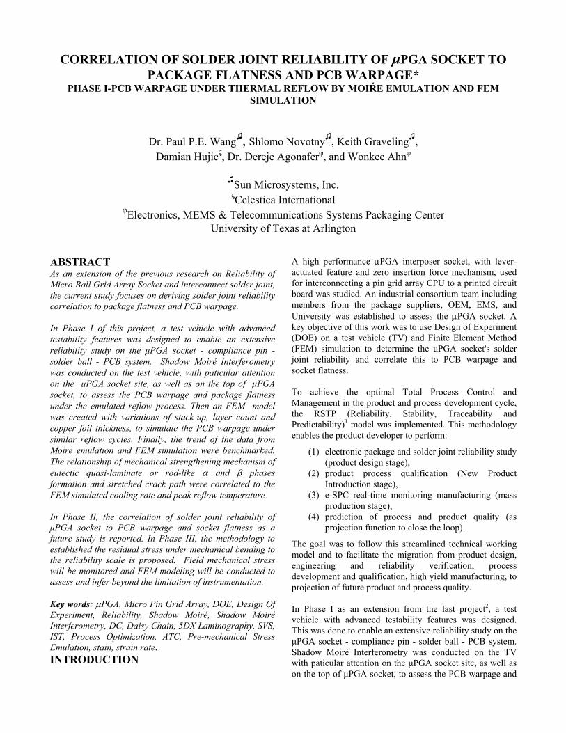
CORRELATION OF SOLDER JOINT RELIABILITY OF μPGA SOCKET TO PACKAGE FLATNESS AND PCB WARPAGE*
PHASE I-PCB WARPAGE UNDER THERMAL REFLOW BY MOIŔE EMULATION AND FEM SIMULATION
Dr. Paul P.E. Wang♫, Shlomo Novotny♫, Keith Graveling♫, Damian Hujicς, Dr. Dereje Agonaferφ, and Wonkee Ahnφ
♫Sun Microsystems, Inc. ςCelestica International
φElectronics, MEMS & Telecommunications Systems Packaging Center University of Texas at Arlington
ABSTRACT As an extension of the previous research on Reliability of Micro Ball Grid Array Socket and interconnect solder joint, the current study focuses on deriving solder joint reliability correlation to package flatness and PCB warpage. In Phase I of this project, a test vehicle with advanced testability features was designed to enable an extensive reliability study on the μPGA socket - compliance pin - solder ball - PCB system. Shadow Moiré Interferometry was conducted on the test vehicle, with paticular attention on the μPGA socket site, as well as on the top of μPGA socket, to assess the PCB warpage and package flatness under the emulated reflow process. Then an FEM model was created with variations of stack-up, layer count and copper foil thickness, to simulate the PCB warpage under similar reflow cycles. Finally, the trend of the data from Moire emulation and FEM simulation were benchmarked. The relationship of mechanical strengthening mechanism of eutectic quasi-laminate or rod-like α and β phases formation and stretched crack path were correlated to the FEM simulated cooling rate and peak reflow temperature In Phase II, the correlation of solder joint reliability of μPGA socket to PCB warpage and socket flatness as a future study is reported. In Phase III, the methodology to established the residual stress under mechanical bending to the reliability scale is proposed. Field mechanical stress will be monitored and FEM modeling will be conducted to assess and infer beyond the limitation of instrumentation. Key words: μPGA, Micro Pin Grid Array, DOE, Design Of Experiment, Reliability, Shadow Moiré, Shadow Moiré Interferometry, DC, Daisy Chain, 5DX Laminography, SVS, IST, Process Optimization, ATC, Pre-mechanical Stress Emulation, stain, strain rate. INTRODUCTION
A high performance μPGA interposer socket, with lever-actuated feature and zero insertion force mechanism, used for interconnecting a pin grid array CPU to a printed circuit board was studied. An industrial consortium team including members from the package suppliers, OEM, EMS, and University was established to assess the μPGA socket. A key objective of this work was to use Design of Experiment (DOE) on a test vehicle (TV) and Finite Element Method (FEM) simulation to determine the uPGA socket's solder joint reliability and correlate this to PCB warpage and socket flatness. To achieve the optimal Total Process Control and Management in the product and process development cycle, the RSTP (Reliability, Stability, Traceability and Predictability)1 model was implemented. This methodology enables the product developer to perform:
(1) electronic package and solder joint reliability study (product design stage),
(2) product process qualification (New Product Introduction stage),
(3) e-SPC real-time monitoring manufacturing (mass production stage),
(4) prediction of process and product quality (as projection function to close the loop).
The goal was to follow this streamlined technical working model and to facilitate the migration from product design, engineering and reliability verification, process development and qualification, high yield manufacturing, to projection of future product and process quality. In Phase I as an extension from the last project2, a test vehicle with advanced testability features was designed. This was done to enable an extensive reliability study on the μPGA socket - compliance pin - solder ball - PCB system. Shadow Moiré Interferometry was conducted on the TV with paticular attention on the μPGA socket site, as well as on the top of μPGA socket, to assess the PCB warpage and
package flatness under the emulated reflow process. Then an FEM model was created with variations of stackup, layer count and copper foil thickness, to simulate the PCB warpage under similar reflow cycles. Finally, the trend of the data from Moire emulation and FEM simulation were benchmarked. The relationship of mechanical strengthening mechanism of eutectic quasi-laminate or rod-like α and β phases formation and stretched crack path were correlated to the simulated cooling rate and peak reflow temperature by FEM.
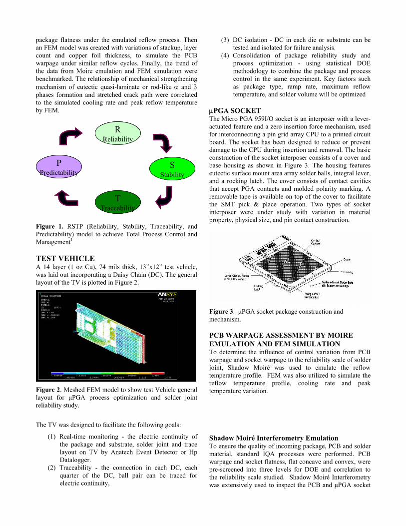
RReliability
PPredictability
TTraceability
SStability
RReliability
PPredictability
TTraceability
SStability
Figure 1. RSTP (Reliability, Stability, Traceability, and Predictability) model to achieve Total Process Control and Management1
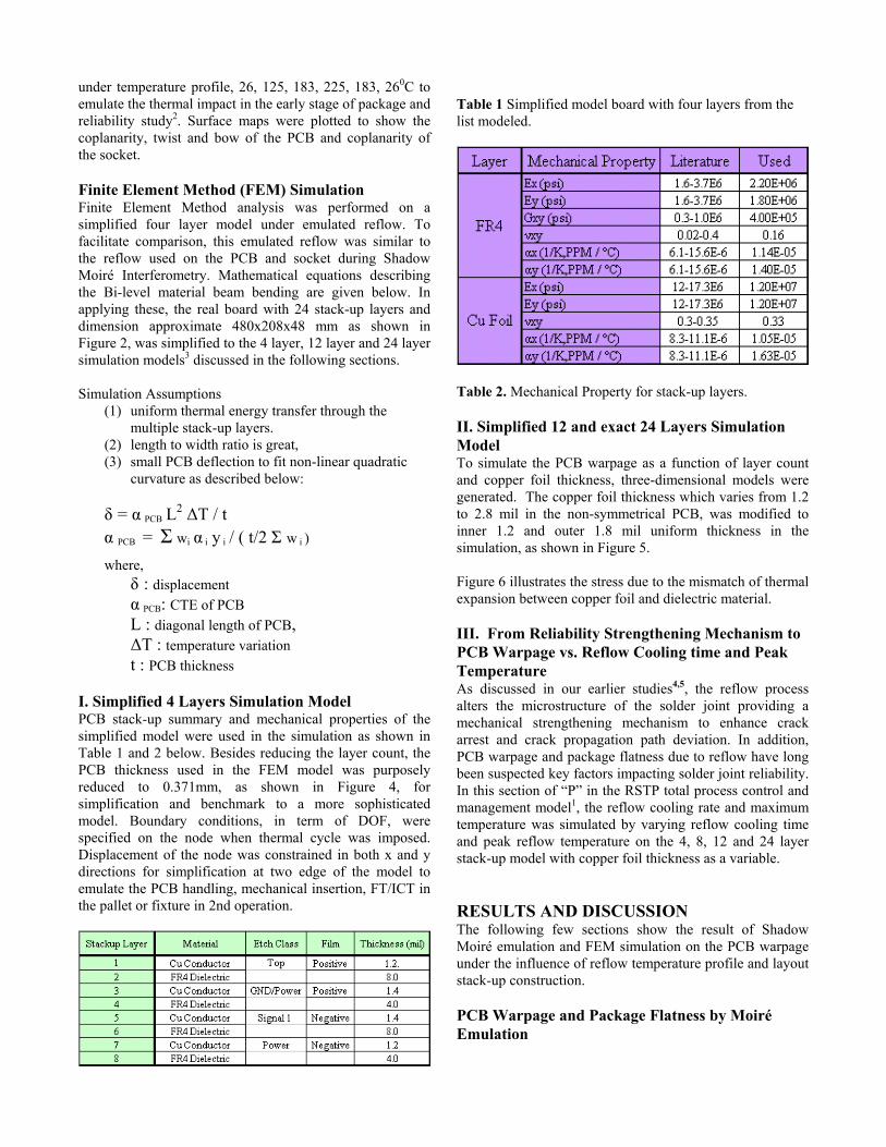
TEST VEHICLE A 14 layer (1 oz Cu), 74 mils thick, 13”x12” test vehicle, was laid out incorporating a Daisy Chain (DC). The general layout of the TV is plotted in Figure 2.
Figure 2. Meshed FEM model to show test Vehicle general layout for μPGA process optimization and solder joint reliability study.
The TV was designed to facilitate the following goals:
(1) Real-time monitoring - the electric continuity of the package and substrate, solder joint and trace layout on TV by Anatech Event Detector or Hp Datalogger.
(2) Traceability - the connection in each DC, each quarter of the DC, ball pair can be traced for electric continuity,
(3) DC isolation - DC in each die or substrate can be tested and isolated for failure analysis.
(4) Consolidation of package reliability study and process optimization - using statistical DOE methodology to combine the package and process control in the same experiment. Key factors such as package type, ramp rate, maximum reflow temperature, and solder volume will be optimized
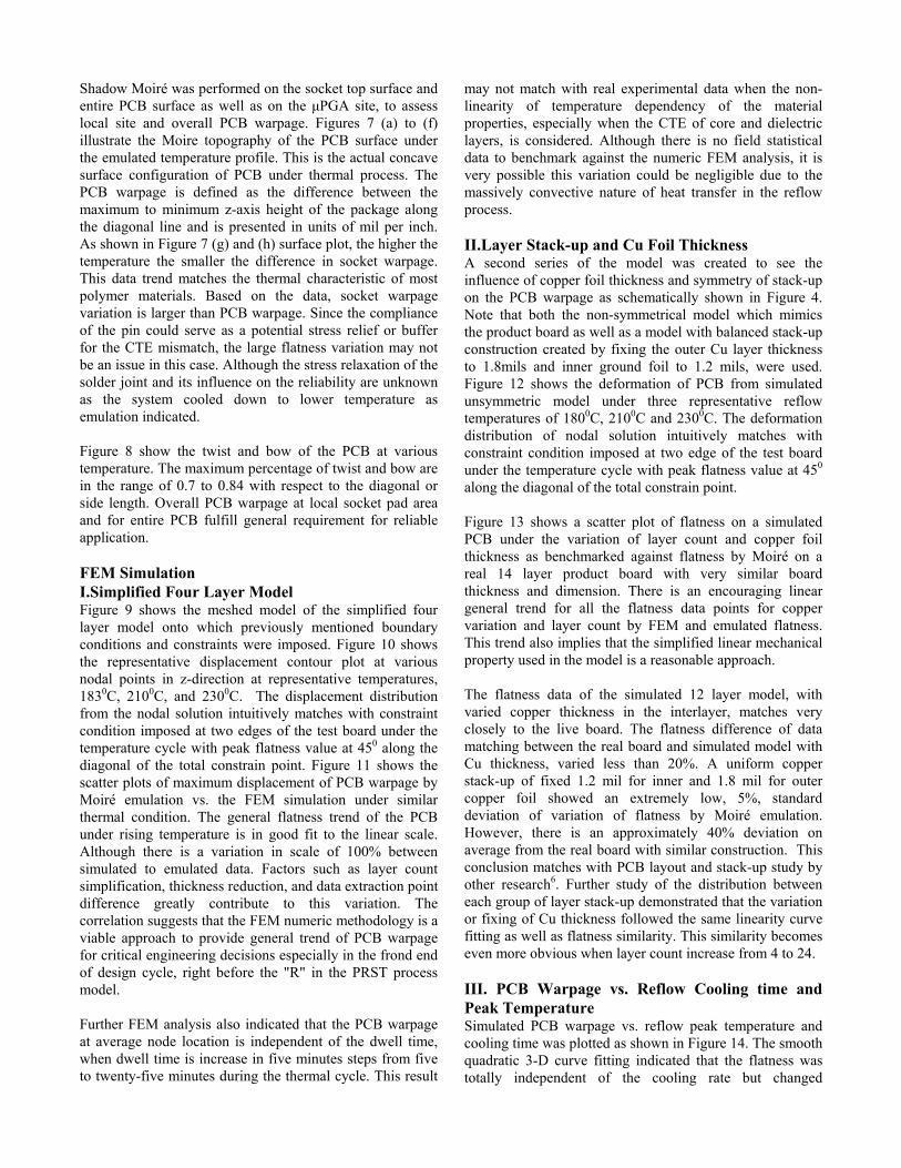
μPGA SOCKET The Micro PGA 959I/O socket is an interposer with a lever-actuated feature and a zero insertion force mechanism, used for interconnecting a pin grid array CPU to a printed circuit board. The socket has been designed to reduce or prevent damage to the CPU during insertion and removal. The basic construction of the socket interposer consists of a cover and base housing as shown in Figure 3. The housing features eutectic surface mount area array solder balls, integral lever, and a rocking latch. The cover consists of contact cavities that accept PGA contacts and molded polarity marking. A removable tape is available on top of the cover to facilitate the SMT pick & place operation. Two types of socket interposer were under study with variation in material property, physical size, and pin contact construction.
Figure 3. μPGA socket package construction and mechanism. PCB WARPAGE ASSESSMENT BY MOIRE EMULATION AND FEM SIMULATION To determine the influence of control variation from PCB warpage and socket warpage to the reliability scale of solder joint, Shadow Moiré was used to emulate the reflow temperature profile. FEM was also utilized to simulate the reflow temperature profile, cooling rate and peak temperature variation. Shadow Moiré Interferometry Emulation To ensure the quality of incoming package, PCB and solder material, standard IQA processes were performed. PCB warpage and socket flatness, flat concave and convex, were pre-screened into three levels for DOE and correlation to the reliability scale studied. Shadow Moiré Interferometry was extensively used to inspect the PCB and μPGA socket
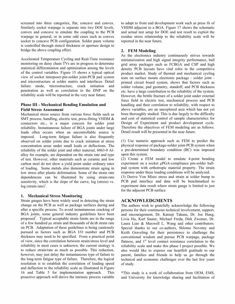
under temperature profile, 26, 125, 183, 225, 183, 260C to emulate the thermal impact in the early stage of package and reliability study2. Surface maps were plotted to show the coplanarity, twist and bow of the PCB and coplanarity of the socket. Finite Element Method (FEM) Simulation Finite Element Method analysis was performed on a simplified four layer model under emulated reflow. To facilitate comparison, this emulated reflow was similar to the reflow used on the PCB and socket during Shadow Moiré Interferometry. Mathematical equations describing the Bi-level material beam bending are given below. In applying these, the real board with 24 stack-up layers and dimension approximate 480x208x48 mm as shown in Figure 2, was simplified to the 4 layer, 12 layer and 24 layer simulation models3 discussed in the following sections. Simulation Assumptions
(1) uniform thermal energy transfer through the multiple stack-up layers.
(2) length to width ratio is great, (3) small PCB deflection to fit non-linear quadratic
curvature as described below: δ = α PCB L2 ΔT / t α PCB = Σ wi α i y i / ( t/2 Σ w i )
where, δ : displacement α PCB: CTE of PCB L : diagonal length of PCB, ΔT : temperature variation t : PCB thickness
I. Simplified 4 Layers Simulation Model PCB stack-up summary and mechanical properties of the simplified model were used in the simulation as shown in Table 1 and 2 below. Besides reducing the layer count, the PCB thickness used in the FEM model was purposely reduced to 0.371mm, as shown in Figure 4, for simplification and benchmark to a more sophisticated model. Boundary conditions, in term of DOF, were specified on the node when thermal cycle was imposed. Displacement of the node was constrained in both x and y directions for simplification at two edge of the model to emulate the PCB handling, mechanical insertion, FT/ICT in the pallet or fixture in 2nd operation.
Table 1 Simplified model board with four layers from the list modeled.
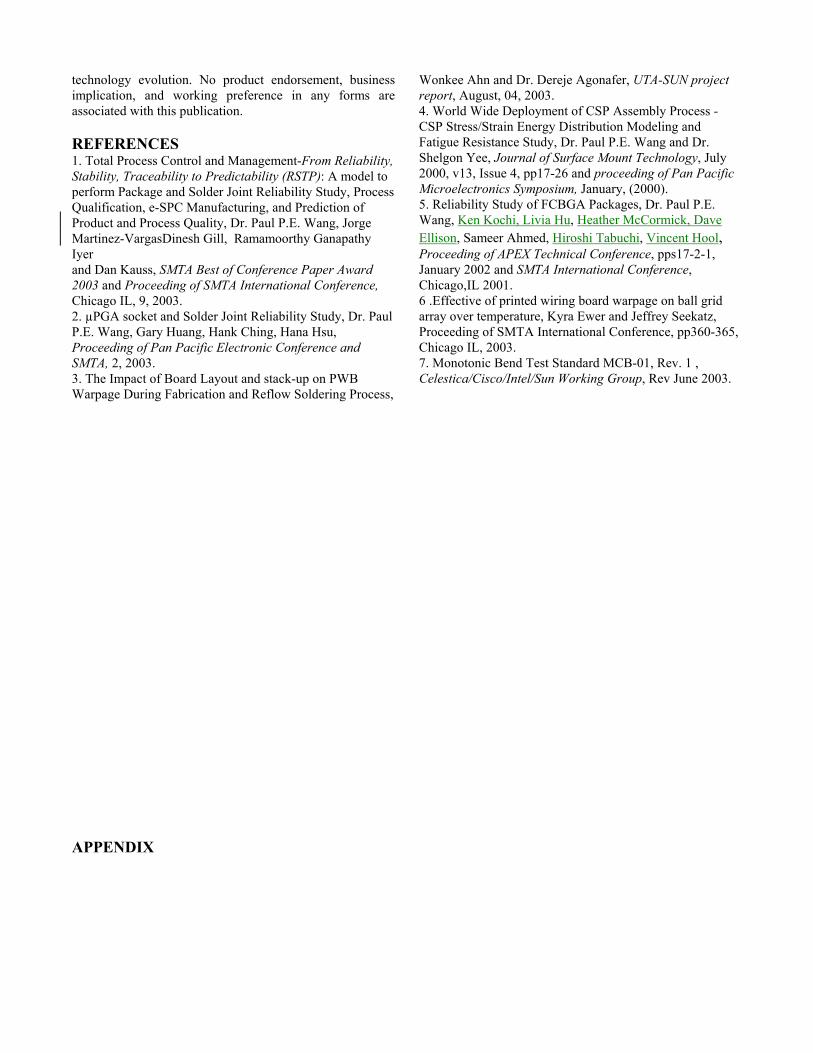
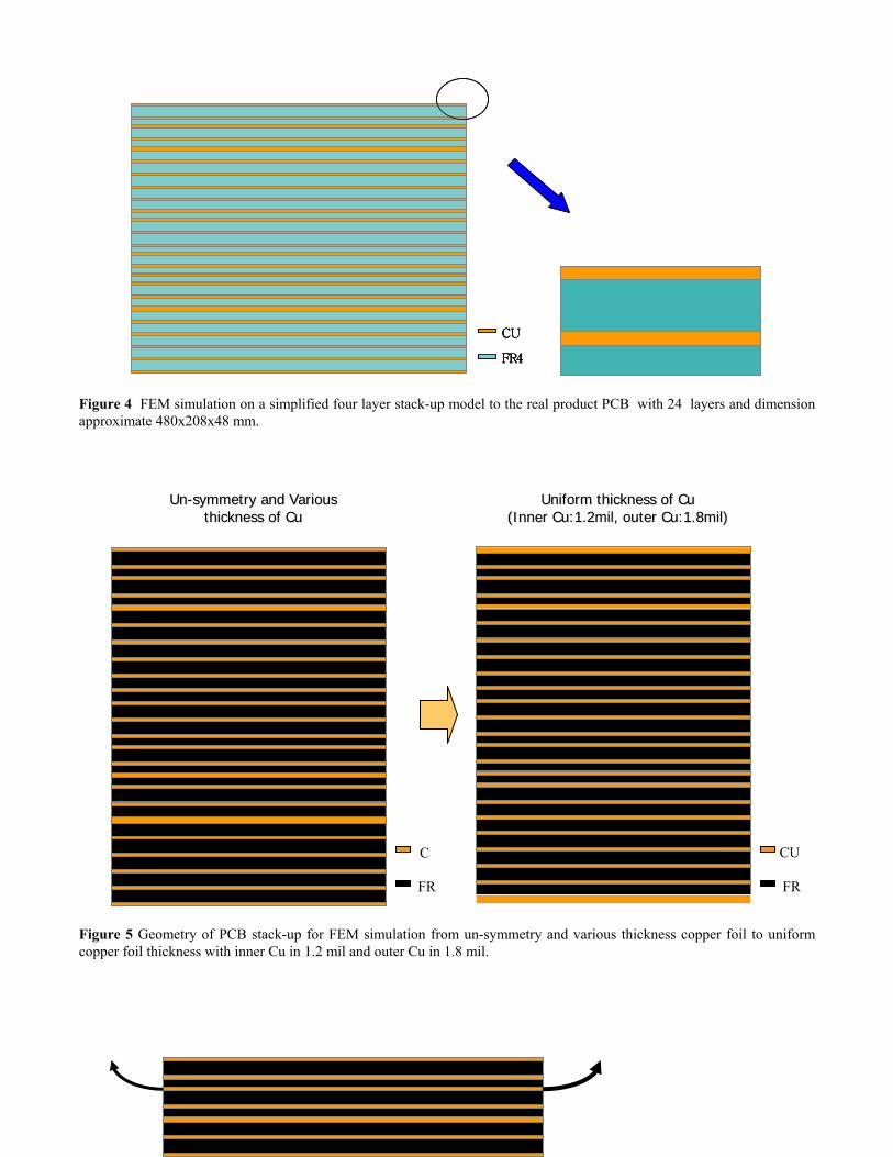
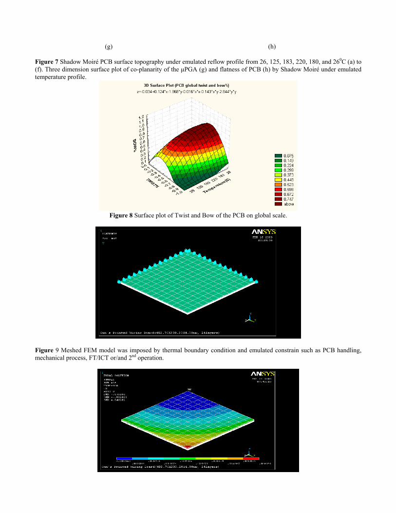
Table 2. Mechanical Property for stack-up layers. II. Simplified 12 and exact 24 Layers Simulation Model To simulate the PCB warpage as a function of layer count and copper foil thickness, three-dimensional models were generated. The copper foil thickness which varies from 1.2 to 2.8 mil in the non-symmetrical PCB, was modified to inner 1.2 and outer 1.8 mil uniform thickness in the simulation, as shown in Figure 5. Figure 6 illustrates the stress due to the mismatch of thermal expansion between copper foil and dielectric material. III. From Reliability Strengthening Mechanism to PCB Warpage vs. Reflow Cooling time and Peak Temperature As discussed in our earlier studies4,5, the reflow process alters the microstructure of the solder joint providing a mechanical strengthening mechanism to enhance crack arrest and crack propagation path deviation. In addition, PCB warpage and package flatness due to reflow have long been suspected key factors impacting solder joint reliability. In this section of “P” in the RSTP total process control and management model1, the reflow cooling rate and maximum temperature was simulated by varying reflow cooling time and peak reflow temperature on the 4, 8, 12 and 24 layer stack-up model with copper foil thickness as a variable. RESULTS AND DISCUSSION The following few sections show the result of Shadow Moiré emulation and FEM simulation on the PCB warpage under the influence of reflow temperature profile and layout stack-up construction. PCB Warpage and Package Flatness by Moiré Emulation
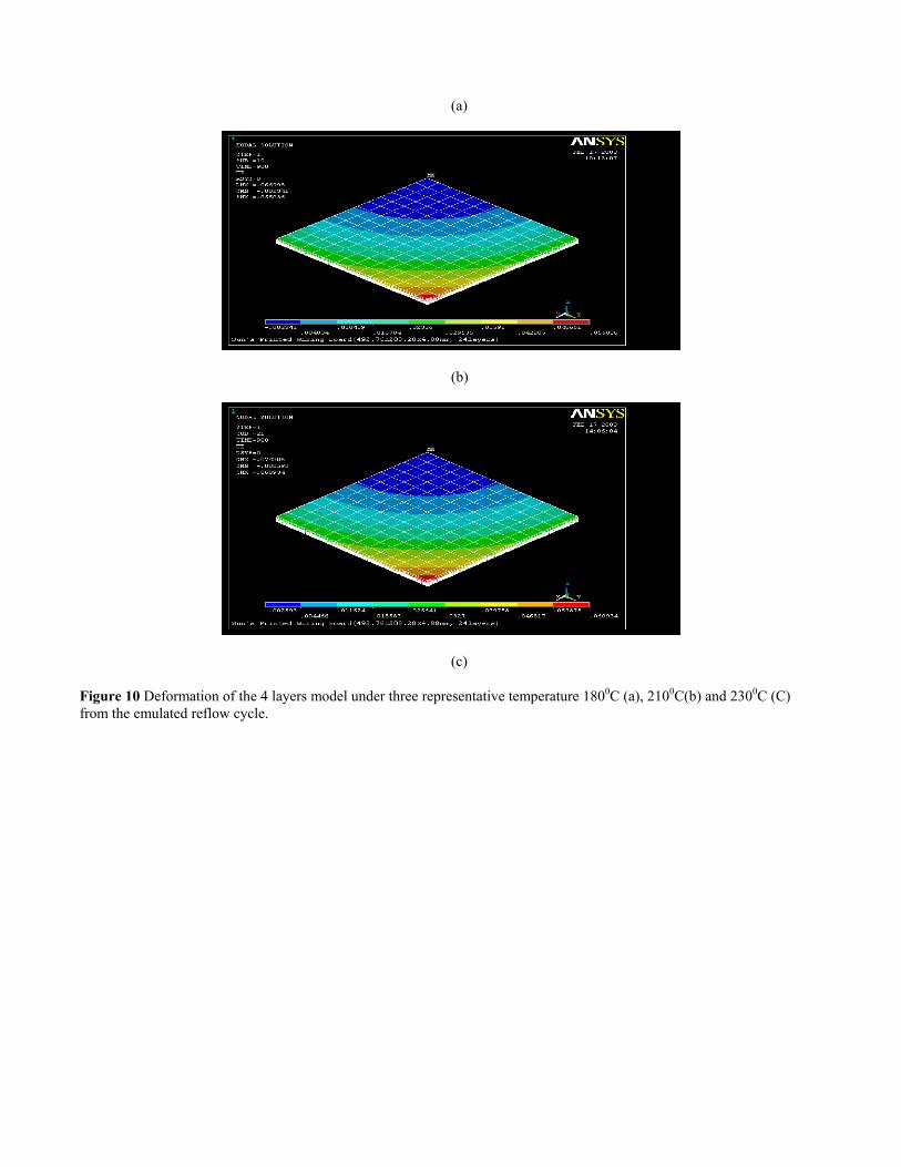
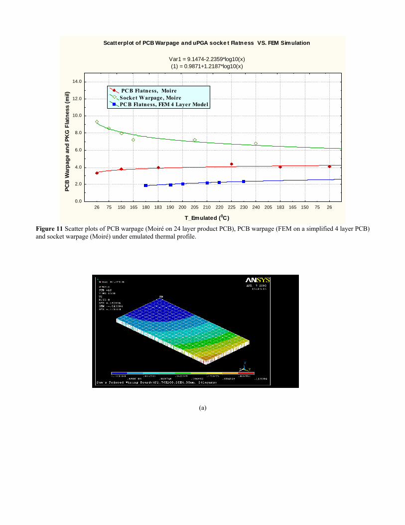
Shadow Moiré was performed on the socket top surface and entire PCB surface as well as on the μPGA site, to assess local site and overall PCB warpage. Figures 7 (a) to (f) illustrate the Moire topography of the PCB surface under the emulated temperature profile. This is the actual concave surface configuration of PCB under thermal process. The PCB warpage is defined as the difference between the maximum to minimum z-axis height of the package along the diagonal line and is presented in units of mil per inch. As shown in Figure 7 (g) and (h) surface plot, the higher the temperature the smaller the difference in socket warpage. This data trend matches the thermal characteristic of most polymer materials. Based on the data, socket warpage variation is larger than PCB warpage. Since the compliance of the pin could serve as a potential stress relief or buffer for the CTE mismatch, the large flatness variation may not be an issue in this case. Although the stress relaxation of the solder joint and its influence on the reliability are unknown as the system cooled down to lower temperature as emulation indicated. Figure 8 show the twist and bow of the PCB at various temperature. The maximum percentage of twist and bow are in the range of 0.7 to 0.84 with respect to the diagonal or side length. Overall PCB warpage at local socket pad area and for entire PCB fulfill general requirement for reliable application. FEM Simulation I.Simplified Four Layer Model Figure 9 shows the meshed model of the simplified four layer model onto which previously mentioned boundary conditions and constraints were imposed. Figure 10 shows the representative displacement contour plot at various nodal points in z-direction at representative temperatures, 1830C, 2100C, and 2300C. The displacement distribution from the nodal solution intuitively matches with constraint condition imposed at two edges of the test board under the temperature cycle with peak flatness value at 450 along the diagonal of the total constrain point. Figure 11 shows the scatter plots of maximum displacement of PCB warpage by Moiré emulation vs. the FEM simulation under similar thermal condition. The general flatness trend of the PCB under rising temperature is in good fit to the linear scale. Although there is a variation in scale of 100% between simulated to emulated data. Factors such as layer count simplification, thickness reduction, and data extraction point difference greatly contribute to this variation. The correlation suggests that the FEM numeric methodology is a viable approach to provide general trend of PCB warpage for critical engineering decisions especially in the frond end of design cycle, right before the "R" in the PRST process model. Further FEM analysis also indicated that the PCB warpage at average node location is independent of the dwell time, when dwell time is increase in five minutes steps from five to twenty-five minutes during the thermal cycle. This result
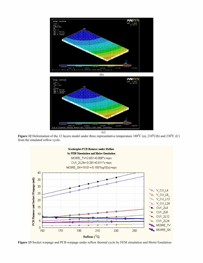
may not match with real experimental data when the non-linearity of temperature dependency of the material properties, especially when the CTE of core and dielectric layers, is considered. Although there is no field statistical data to benchmark against the numeric FEM analysis, it is very possible this variation could be negligible due to the massively convective nature of heat transfer in the reflow process. II.Layer Stack-up and Cu Foil Thickness A second series of the model was created to see the influence of copper foil thickness and symmetry of stack-up on the PCB warpage as schematically shown in Figure 4. Note that both the non-symmetrical model which mimics the product board as well as a model with balanced stack-up construction created by fixing the outer Cu layer thickness to 1.8mils and inner ground foil to 1.2 mils, were used. Figure 12 shows the deformation of PCB from simulated unsymmetric model under three representative reflow temperatures of 1800C, 2100C and 2300C. The deformation distribution of nodal solution intuitively matches with constraint condition imposed at two edge of the test board under the temperature cycle with peak flatness value at 450 along the diagonal of the total constrain point. Figure 13 shows a scatter plot of flatness on a simulated PCB under the variation of layer count and copper foil thickness as benchmarked against flatness by Moiré on a real 14 layer product board with very similar board thickness and dimension. There is an encouraging linear general trend for all the flatness data points for copper variation and layer count by FEM and emulated flatness. This trend also implies that the simplified linear mechanical property used in the model is a reasonable approach. The flatness data of the simulated 12 layer model, with varied copper thickness in the interlayer, matches very closely to the live board. The flatness difference of data matching between the real board and simulated model with Cu thickness, varied less than 20%. A uniform copper stack-up of fixed 1.2 mil for inner and 1.8 mil for outer copper foil showed an extremely low, 5%, standard deviation of variation of flatness by Moiré emulation. However, there is an approximately 40% deviation on average from the real board with similar construction. This conclusion matches with PCB layout and stack-up study by other research6. Further study of the distribution between each group of layer stack-up demonstrated that the variation or fixing of Cu thickness followed the same linearity curve fitting as well as flatness similarity. This similarity becomes even more obvious when layer count increase from 4 to 24. III. PCB Warpage vs. Reflow Cooling time and Peak Temperature Simulated PCB warpage vs. reflow peak temperature and cooling time was plotted as shown in Figure 14. The smooth quadratic 3-D curve fitting indicated that the flatness was totally independent of the cooling rate but changed
drastically with peak temperature. The simulated PCB warpage under the peak reflow temperature followed similar trend to the Moiré emulation as shown in Figure 10. However, there is no clear rationale to explain the decreasing flatness from 220 to 2250C. The data distribution of the flatness to cooling rate needs further Moiré confirmation, but lower cooling dependency will offer a good opportunity to reduce or limit spacing growth between α and β eutectic phases as indicated in our earlier study4,5. Reducing interface spacing will create more α−β interface areas, which in turn will then effectively blunt the phase slip and deformation created by external forces. 1. Strengthening mechanism of α−β rod-like phases The mechanical strength of the eutectic solder was greatly enhanced by the rod-like structure formed during the fast solidification at the end of the reflow process. The temperature profile used in this qualification procedure provided a fast cooling process during reflow. Consequently the spacing between α and β phases was reduced. As as result, this created more α−β interface areas, which will then effectively blunt the phase slip and deformation created by external forces. 2. Strengthening mechanism from stretched crack path In general, crack nucleates under cyclic load at the Pb-rich α phase near the brittle IMC interface. The crack will preferentially walk along the interface of the rod-like phases of α−β until the external energy is exhausted or tougher IMC and Sn-rich β phase is encountered. Once the crack encounters a β phase or IMC, the crack can bust through the second phase or deviate its path to release its energy. The strength of the material is enhanced as the crack propagation path is stretched in a zig-zag fashion. CONCLUSION To assess the board level reliability of 959I/O μPGA socket interposer and optimize the process window, a test vehicle was designed. Advanced features were laid out on the test board to facilitate the real-time monitoring, failure traceability, daisy chain isolation, component isolation, daisy chain jump out, and consolidation of package reliability study and process optimization. Shadow Moiré was performed with emulated reflow process to inspect the package flatness and PCB warpage, of the whole PCB, as well as of local μPGA pad area. Socket flatness variation is larger at room temperature as compared to PCB specification. Less severe flatness is observed at high temperature where solder interconnect between socket and PCB occurs. Although the stress relaxation of the solder joint and its influence to the reliability scale is unknown when the socket-solder-pad system cooled down to lower temperature as in emulation process.
FEM simulation showed that the displacement distribution of nodal solution intuitively matches with constraint condition imposed on the model. The general trend of the PCB warpage under rising temperature is a good linear fit. Large PCB warpage variation in the scale of 100% between simulated FEM to emulated Moiré data for simplified model with lower layer stack-up construction due to possible non-linearity of material property, thickness reduction, and data extraction point difference. FEM analysis also indicated that the PCB warpage at average node location is independent of the dwell time. This result may not match with real experimental data when the non-linearity of temperature dependency of the material properties, especially the CTE of core and dielectric layers, is considered. Although there is no field statistical data to benchmark against, it is very possible this variation could be negligibly small due to the massively convective nature of heat transfer in the reflow process. Encouraging linear fit, extremely low variation and reasonably low warpage difference between FEM and Moiré under reflow cycle for PCB and model with uniform copper thickness and larger layer count was observed. Furthermore, FEM simulation also demonstrates good fit to the field data with respect to the variation of reflow peak temperature. Further confirmation is required on the sudden PCB warpage drop at super high reflow temperature. Finally, the de-coupling of cooling rate to the PCB warpage offers a good opportunity to reflow the package-solder- PCB pad system with high cooling rate and in turn to maintain low PCB warpage, reduce/limit spacing growth between α and β eutectic solder phases. As the result of reduction interface spacing, soldering system will create more α−β interface areas which will then effectively blunt the phase slip and deformation and stretch and deviates the effective crack propagation path. An optimal system with low PCB warpage and mechanical strengthened solder joint is reached. These current correlation's and inferences suggest that the FEM numeric methodology is a viable approach to provide general trends for critical engineering decisions, especially in the front end of design and process development cycles right before the “R” in the PRST process model. FUTURE STUDY Phase II- Correlation of Solder Joint Reliability of μPGA Socket to Package Flatness and PCB Warpage* To study the correlation of PCB warpage and package flatness to solder joint reliability, the consolidation of package reliability and process optimization DOE methodologies 2 is used in phase II of the project. Two types of socket with variation of pin contact, material property, and geometry are used as process control variables. Pre-warped PCBs are intentionally manufactured and pre-
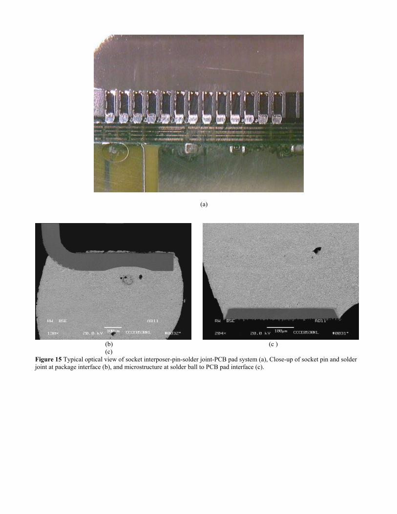
screened into three categories, flat, concave and convex. Similarly socket warpage is separate into two DOE levels, convex and concave to emulate the coupling to the PCB warpage in general, or in some odd cases such as convex socket to concave PCB configuration. Solder paste volume is controlled through stencil thickness or aperture design to bridge the above coupling effect. Accelerated Temperature Cycling and Real-Time resistance monitoring on daisy chain TVs are in progress to determine statistical differentiation and optimization among the levels of the control variables. Figure 15 shows a typical optical view of socket interposer-pin-solder joint-PCB pad system and microstructure at solder matrix and interfaces. Detail failure mode, microstructure, crack initiation and penetration as well as correlation to the DNP on the reliability scale will be reported in the very near future. Phase III - Mechanical Bending Emulation and Field Stress Assessment Mechanical stress source from various force fields such as SMT process, handling, electric test, press-fitting VHDM & connectors etc., is a major concern for solder joint reliability. Instantaneous failure of BGA joints under large loads often occurs when an uncontrollable source is imposed. Long-term fatigue failure is also frequently observed on solder joints due to crack initiation at stress concentration areas under small loads or deflections. The reliability of the solder joint and other material, 6063-0 Al-alloy for example, are dependent on the strain rate and type of test. However, other materials such as ceramic and low carbon steel do not show a yield point under ordinary rates of loading. Some metals also demonstrate strain aging in low stress after plastic deformation. Some of the strain rate dependencies can be illustrated by using strain-rate sensitivity, which is the slope of the curve, log (stress) vs. log (strain rate)1. 1. Mechanical Stress Monitoring Strain gauges have been widely used in detecting the strain change on the PCB as well as package surfaces during and after a specific process. To avoid instantaneous cracking of BGA joints, some general industry guidelines have been proposed7. Typical acceptable strain limits are in the range of a few hundred με strain and thousands of dε/dt strain rate on PCB. Adaptation of these guidelines is being cautiously pursued as factors such as BGA I/O number and PCB thickness may need to be specified. From a practical point of view, since the correlation between strain/stress level and reliability in most cases is unknown, the current strategy is to reduce strain/rate as much as possible. This reduction, however, may just delay the instantaneous type of failure to the long-term fatigue type of failure. Therefore, the logical resolution is to establish the correlation of loading speed and deflection to the reliability scale as illustrated in Figure 16 and Table 5 for implementation approach. This proactive approach will derive the intrinsic process variable
to adapt to front end development work such as press fit of VHDM adjacent to a BGA. Figure 17 shows the schematic and actual test setup for DOE and test result to exploit the residue stress relationship to the reliability scale will be reported in the near future. 2. FEM Modeling As the electronics industry continuously strives towards miniaturization and high signal integrity performance, ball grid array packages such as FCBGA and CSP and high density PCB layouts have vital roles in the competitive product market. Study of thermal and mechanical cycling tests on surface mount electronic package - solder joint - printed circuit board system, shows that factors such as solder volume, pad geometry, standoff, and PCB thickness etc. have a large contribution to the reliability of the system. However, the brittle fracture of a solder joint under external force field in electric test, mechanical process and PCB handling and their correlation to reliability, with respect to above variables, are an unexplored area which has not yet been thoroughly studied. This is due largely to the difficulty and cost of statistical control of sample characteristics for Design of Experiment and product development cycle. Therefore the objectives of FEM modeling are as follows. Detail result will be presented in the near future. (1) Use numeric approach such as FEM to predict the physical response of package-solder joint-PCB system when a pre-determined boundary condition (BC) was imposed upon this system. (2) Create a FEM model to emulate 4-point bending experiment on a socket μPGA-compliance pin-solder ball-pad system with orthotropic material property. The strain response under these loading conditions will be analyzed. (3) Derive Von Mises stress and strain at solder bump to PCB pad interface and data will be benchmarked to experiment data result where strain gauge is limited to just for the adjacent PCB surface. ACKNOWLEDGMENTS The authors wish to gratefully acknowledge the following persons for their continuous technical involvement, support, and encouragement, Dr. Katsuji Takasu, Dr. Joe Hung, Livia Hu, Karl Sauter, Michael Freda, Dirk Zwemer, Dr. Laura Liao & Maxwell L. Wang and other contributors. Special thanks to our co-authors, Shlomo Novotny and Keith Graveling for their persistence to challenge the conventional wisdom and pursue PCB warpage, package flatness, and 1st level contact resistance correlation to the reliability scale and make this phase I project possible. We also would like to express our heartfelt gratitude to our parent, families and friends to help us go through the technical and economic challenges over the last few years of study. *This study is a work of collaboration from OEM, EMS, and University for knowledge sharing and facilitation of
technology evolution. No product endorsement, business implication, and working preference in any forms are associated with this publication. REFERENCES 1. Total Process Control and Management-From Reliability, Stability, Traceability to Predictability (RSTP): A model to perform Package and Solder Joint Reliability Study, Process Qualification, e-SPC Manufacturing, and Prediction of Product and Process Quality, Dr. Paul P.E. Wang, Jorge Martinez-VargasDinesh Gill, Ramamoorthy Ganapathy Iyer and Dan Kauss, SMTA Best of Conference Paper Award 2003 and Proceeding of SMTA International Conference, Chicago IL, 9, 2003. 2. µPGA socket and Solder Joint Reliability Study, Dr. Paul P.E. Wang, Gary Huang, Hank Ching, Hana Hsu, Proceeding of Pan Pacific Electronic Conference and SMTA, 2, 2003. 3. The Impact of Board Layout and stack-up on PWB Warpage During Fabrication and Reflow Soldering Process,
Wonkee Ahn and Dr. Dereje Agonafer, UTA-SUN project report, August, 04, 2003. 4. World Wide Deployment of CSP Assembly Process - CSP Stress/Strain Energy Distribution Modeling and Fatigue Resistance Study, Dr. Paul P.E. Wang and Dr. Shelgon Yee, Journal of Surface Mount Technology, July 2000, v13, Issue 4, pp17-26 and proceeding of Pan Pacific Microelectronics Symposium, January, (2000). 5. Reliability Study of FCBGA Packages, Dr. Paul P.E. Wang, Ken Kochi, Livia Hu, Heather McCormick, Dave Ellison, Sameer Ahmed, Hiroshi Tabuchi, Vincent Hool, Proceeding of APEX Technical Conference, pps17-2-1, January 2002 and SMTA International Conference, Chicago,IL 2001. 6 .Effective of printed wiring board warpage on ball grid array over temperature, Kyra Ewer and Jeffrey Seekatz, Proceeding of SMTA International Conference, pp360-365, Chicago IL, 2003. 7. Monotonic Bend Test Standard MCB-01, Rev. 1 , Celestica/Cisco/Intel/Sun Working Group, Rev June 2003.
APPENDIX
CU
FR4
CU
FR4
CU
FR4
CU
FR4
Figure 4 FEM simulation on a simplified four layer stack-up model to the real product PCB with 24 layers and dimension approximate 480x208x48 mm. Figure 5 Geometry of PCB stack-up for FEM simulation from un-symmetry and various thickness copper foil to uniform copper foil thickness with inner Cu in 1.2 mil and outer Cu in 1.8 mil.
C
FR
CU
FR
UUnn--ssyymmmmeettrryy aanndd VVaarriioouuss tthhiicckknneessss ooff CCuu
UUnniiffoorrmm tthhiicckknneessss ooff CCuu ((IInnnneerr CCuu::11..22mmiill,, oouutteerr CCuu::11..88mmiill))
Figure 6 Thermal stress induced from CTE variation between copper foil and dielectric material.
(a)
(d)
(c) (b)
(f) (e)
(g) (h) Figure 7 Shadow Moiré PCB surface topography under emulated reflow profile from 26, 125, 183, 220, 180, and 260C (a) to (f). Three dimension surface plot of co-planarity of the μPGA (g) and flatness of PCB (h) by Shadow Moiré under emulated temperature profile.
Figure 8 Surface plot of Twist and Bow of the PCB on global scale.
Figure 9 Meshed FEM model was imposed by thermal boundary condition and emulated constrain such as PCB handling, mechanical process, FT/ICT or/and 2nd operation.
(a)
(b)
(c)
Figure 10 Deformation of the 4 layers model under three representative temperature 1800C (a), 2100C(b) and 2300C (C) from the emulated reflow cycle.
Scatterplot of PCB Warpage and uPGA socke t Flatness VS. FEM Simulation
Var1 = 9.1474-2.2359*log10(x)(1) = 0.9871+1.2187*log10(x)
T_Emulated (0C)
PCB
War
page
and
PK
G F
latn
ess
(mil)
26 75 150 165 180 183 190 200 205 210 220 225 230 240 205 183 165 150 75 260.0
2.0
4.0
6.0
8.0
10.0
12.0
14.0
PCB Flatness, MoireSocket Warpage, MoirePCB Flatness, FEM 4 Layer Model
Figure 11 Scatter plots of PCB warpage (Moiré on 24 layer product PCB), PCB warpage (FEM on a simplified 4 layer PCB) and socket warpage (Moiré) under emulated thermal profile.
(a)
(b)
(c) Figure 12 Deformation of the 12 layers model under three representative temperature 1800C (a), 2100C(b) and 2300C (C) from the emulated reflow cycle.
Figure 13 Socket warpage and PCB warpage under reflow thermal cycle by FEM simulation and Moiré Emulation.
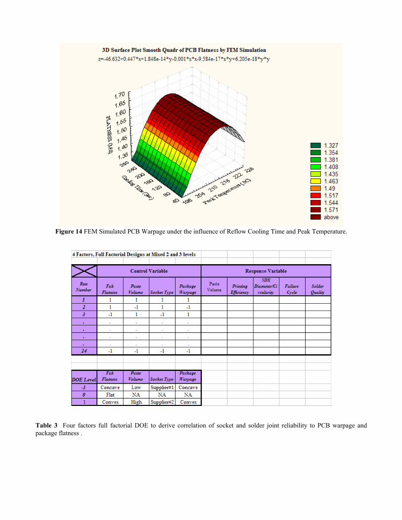
Figure 14 FEM Simulated PCB Warpage under the influence of Reflow Cooling Time and Peak Temperature.
Table 3 Four factors full factorial DOE to derive correlation of socket and solder joint reliability to PCB warpage and package flatness .
(a)
(b) (c ) (c)
Figure 15 Typical optical view of socket interposer-pin-solder joint-PCB pad system (a), Close-up of socket pin and solder joint at package interface (b), and microstructure at solder ball to PCB pad interface (c).
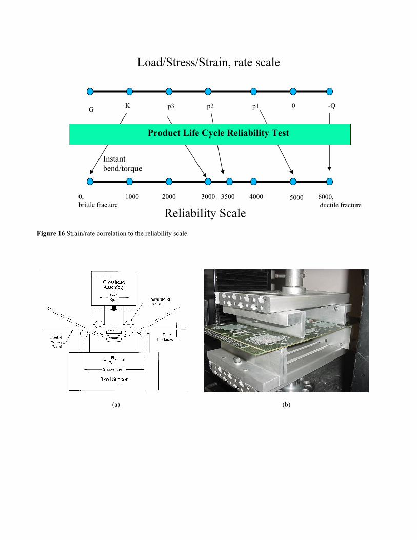
Figure 16 Strain/rate correlation to the reliability scale.
(a) (b)
6000, ductile fracture
Reliability Scale 0, brittle fracture
35001000 2000 4000 5000
Load/Stress/Strain, rate scale
G p2 K p3 p1 0 -Q
Instant bend/torque
3000
Product Life Cycle Reliability Test
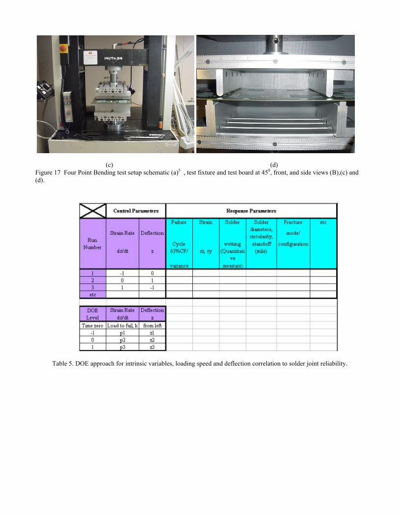
(c) (d) Figure 17 Four Point Bending test setup schematic (a)5 , test fixture and test board at 450, front, and side views (B),(c) and (d).
Table 5. DOE approach for intrinsic variables, loading speed and deflection correlation to solder joint reliability.