CN-0393 Circuit Note - Analog Devices · Circuit Note CN-0393 Circuits from the Lab® reference...
15
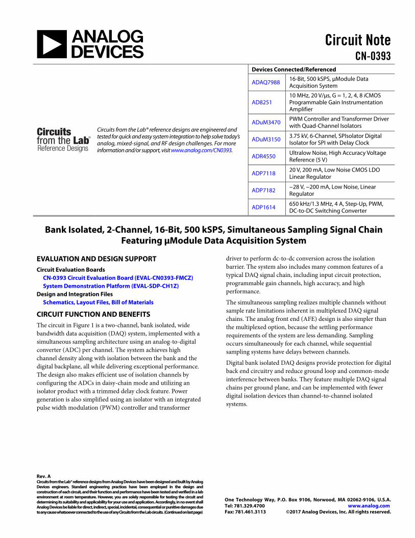
Circuit Note CN-0393 Circuits from the Lab® reference designs are engineered and tested for quick and easy system integration to help solve today’s analog, mixed-signal, and RF design challenges. For more information and/or support, visit www.analog.com/CN0393. Devices Connected/Referenced ADAQ7988 16-Bit, 500 kSPS, μModule Data Acquisition System AD8251 10 MHz, 20 V/µs, G = 1, 2, 4, 8 iCMOS Programmable Gain Instrumentation Amplifier ADuM3470 PWM Controller and Transformer Driver with Quad-Channel Isolators ADuM3150 3.75 kV, 6-Channel, SPIsolator Digital Isolator for SPI with Delay Clock ADR4550 Ultralow Noise, High Accuracy Voltage Reference (5 V) ADP7118 20 V, 200 mA, Low Noise CMOS LDO Linear Regulator ADP7182 −28 V, −200 mA, Low Noise, Linear Regulator ADP1614 650 kHz/1.3 MHz, 4 A, Step-Up, PWM, DC-to-DC Switching Converter Bank Isolated, 2-Channel, 16-Bit, 500 kSPS, Simultaneous Sampling Signal Chain Featuring μModule Data Acquisition System Rev. A Circuits from the Lab® reference designs from Analog Devices have been designed and built by Analog Devices engineers. Standard engineering practices have been employed in the design and construction of each circuit, and their function and performance have been tested and verified in a lab environment at room temperature. However, you are solely responsible for testing the circuit and determining its suitability and applicability for your use and application. Accordingly, in no event shall Analog Devices be liable for direct, indirect, special, incidental, consequential or punitive damages due toanycausewhatsoeverconnectedtotheuseofanyCircuitsfromtheLabcircuits. (Continuedonlastpage) One Technology Way, P.O. Box 9106, Norwood, MA 02062-9106, U.S.A. Tel: 781.329.4700 www.analog.com Fax: 781.461.3113 ©2017 Analog Devices, Inc. All rights reserved. EVALUATION AND DESIGN SUPPORT Circuit Evaluation Boards CN-0393 Circuit Evaluation Board (EVAL-CN0393-FMCZ) System Demonstration Platform (EVAL-SDP-CH1Z) Design and Integration Files Schematics, Layout Files, Bill of Materials CIRCUIT FUNCTION AND BENEFITS The circuit in Figure 1 is a two-channel, bank isolated, wide bandwidth data acquisition (DAQ) system, implemented with a simultaneous sampling architecture using an analog-to-digital converter (ADC) per channel. The system achieves high channel density along with isolation between the bank and the digital backplane, all while delivering exceptional performance. The design also makes efficient use of isolation channels by configuring the ADCs in daisy-chain mode and utilizing an isolator product with a trimmed delay clock feature. Power generation is also simplified using an isolator with an integrated pulse width modulation (PWM) controller and transformer driver to perform dc-to-dc conversion across the isolation barrier. The system also includes many common features of a typical DAQ signal chain, including input circuit protection, programmable gain channels, high accuracy, and high performance. The simultaneous sampling realizes multiple channels without sample rate limitations inherent in multiplexed DAQ signal chains. The analog front end (AFE) design is also simpler than the multiplexed option, because the settling performance requirements of the system are less demanding. Sampling occurs simultaneously for each channel, while sequential sampling systems have delays between channels. Digital bank isolated DAQ designs provide protection for digital back end circuitry and reduce ground loop and common-mode interference between banks. They feature multiple DAQ signal chains per ground plane, and can be implemented with fewer digital isolation devices than channel-to-channel isolated systems.
Transcript of CN-0393 Circuit Note - Analog Devices · Circuit Note CN-0393 Circuits from the Lab® reference...
Circuit Note CN-0393
Circuits from the Lab® reference designs are engineered and tested for quick and easy system integration to help solve today’s analog, mixed-signal, and RF design challenges. For more information and/or support, visit www.analog.com/CN0393.
Devices Connected/Referenced
ADAQ7988 16-Bit, 500 kSPS, μModule Data Acquisition System
AD8251 10 MHz, 20 V/µs, G = 1, 2, 4, 8 iCMOS Programmable Gain Instrumentation Amplifier
ADuM3470 PWM Controller and Transformer Driver with Quad-Channel Isolators
ADuM3150 3.75 kV, 6-Channel, SPIsolator Digital Isolator for SPI with Delay Clock
ADR4550 Ultralow Noise, High Accuracy Voltage Reference (5 V)
ADP7118 20 V, 200 mA, Low Noise CMOS LDO Linear Regulator
ADP7182 −28 V, −200 mA, Low Noise, Linear Regulator
ADP1614 650 kHz/1.3 MHz, 4 A, Step-Up, PWM, DC-to-DC Switching Converter
Bank Isolated, 2-Channel, 16-Bit, 500 kSPS, Simultaneous Sampling Signal Chain Featuring μModule Data Acquisition System
Rev. A Circuits from the Lab® reference designs from Analog Devices have been designed and built by Analog Devices engineers. Standard engineering practices have been employed in the design and construction of each circuit, and their function and performance have been tested and verified in a lab environment at room temperature. However, you are solely responsible for testing the circuit and determining its suitability and applicability for your use and application. Accordingly, in no event shall Analog Devices be liable for direct, indirect, special, incidental, consequential or punitive damages due to any cause whatsoever connected to the use of any Circuits from the Lab circuits. (Continued on last page)
One Technology Way, P.O. Box 9106, Norwood, MA 02062-9106, U.S.A. Tel: 781.329.4700 www.analog.com Fax: 781.461.3113 ©2017 Analog Devices, Inc. All rights reserved.
EVALUATION AND DESIGN SUPPORT Circuit Evaluation Boards
CN-0393 Circuit Evaluation Board (EVAL-CN0393-FMCZ) System Demonstration Platform (EVAL-SDP-CH1Z)
Design and Integration Files Schematics, Layout Files, Bill of Materials
CIRCUIT FUNCTION AND BENEFITS The circuit in Figure 1 is a two-channel, bank isolated, wide bandwidth data acquisition (DAQ) system, implemented with a simultaneous sampling architecture using an analog-to-digital converter (ADC) per channel. The system achieves high channel density along with isolation between the bank and the digital backplane, all while delivering exceptional performance. The design also makes efficient use of isolation channels by configuring the ADCs in daisy-chain mode and utilizing an isolator product with a trimmed delay clock feature. Power generation is also simplified using an isolator with an integrated pulse width modulation (PWM) controller and transformer
driver to perform dc-to-dc conversion across the isolation barrier. The system also includes many common features of a typical DAQ signal chain, including input circuit protection, programmable gain channels, high accuracy, and high performance.
The simultaneous sampling realizes multiple channels without sample rate limitations inherent in multiplexed DAQ signal chains. The analog front end (AFE) design is also simpler than the multiplexed option, because the settling performance requirements of the system are less demanding. Sampling occurs simultaneously for each channel, while sequential sampling systems have delays between channels.
Digital bank isolated DAQ designs provide protection for digital back end circuitry and reduce ground loop and common-mode interference between banks. They feature multiple DAQ signal chains per ground plane, and can be implemented with fewer digital isolation devices than channel-to-channel isolated systems.
CN-0393 Circuit Note
Rev. A | Page 2 of 15
GND2 GND1
SOSSS
SCLKSI
MI
MSSMCLK
MO
DCLK
VVDD2 DD1+5V
REF
GND
VDD
VIO
20Ω
V+
V–
1.8nF
LDO2.2µF10µF
AMP_OUTADC
IN+
IN–
ADAQ7988(B)
ADCN
SDISCK
SDOCNV500Ω2kΩ
1kΩ1.5kΩ
+7.5V +5V
–2.5V
VREF
VREF
G1BG0B
+15V
–15V
CB+
CB–
A1A0
REF
GND
VDD
VIO
20Ω
V+
V–
1.8nF
LDO2.2µF10µF
AMP_OUTADC
IN+
IN–
ADAQ7988(A)
ADCN
SDISCK
SDOCNV
G1AG0A
AD8251(A)
AD8251(B)
500Ω2kΩ
1kΩ1.5kΩ
+7.5V +5V
–2.5V
+15V
–15V
CA+
CA–
A1A0
100kΩ
TRANSFORMER
8.2kΩ
SCHOTTKYDIODE
FULL WAVERECTIFIER
+ISO +16.5V
–ISO
VOA
GND2
FB
VREG
VOBVOCVID
VIAVIBVIC
VOD
GND1
VDD1
X2
X1
SECONDARYSIDE
PRIMARYSIDE
+1.25V
G1AG0AG1BG0B
49.9kΩ
100kΩADP7118
+15V+ISOVIN
GND
VOUT
ADJ
13.3kΩ
150kΩADP7182
–15V–ISOVIN
GND
VOUT
ADJADR4550
+7.5VVIN
GND
VOUT
49.9kΩ
25kΩADP7118
+7.5V+15VVIN
GND
VOUT
ADJADP7118
+5V+7.5VVIN
GND
VOUT
ADJ
ADP7182
–2.5V–15VVIN
GND
VOUTVREF
5V
SDP-H1(FMC)
+3.3V
SPI
PGIAGAIN
+3.3V
ADuM3470
ADuM3150
1570
7-00
1
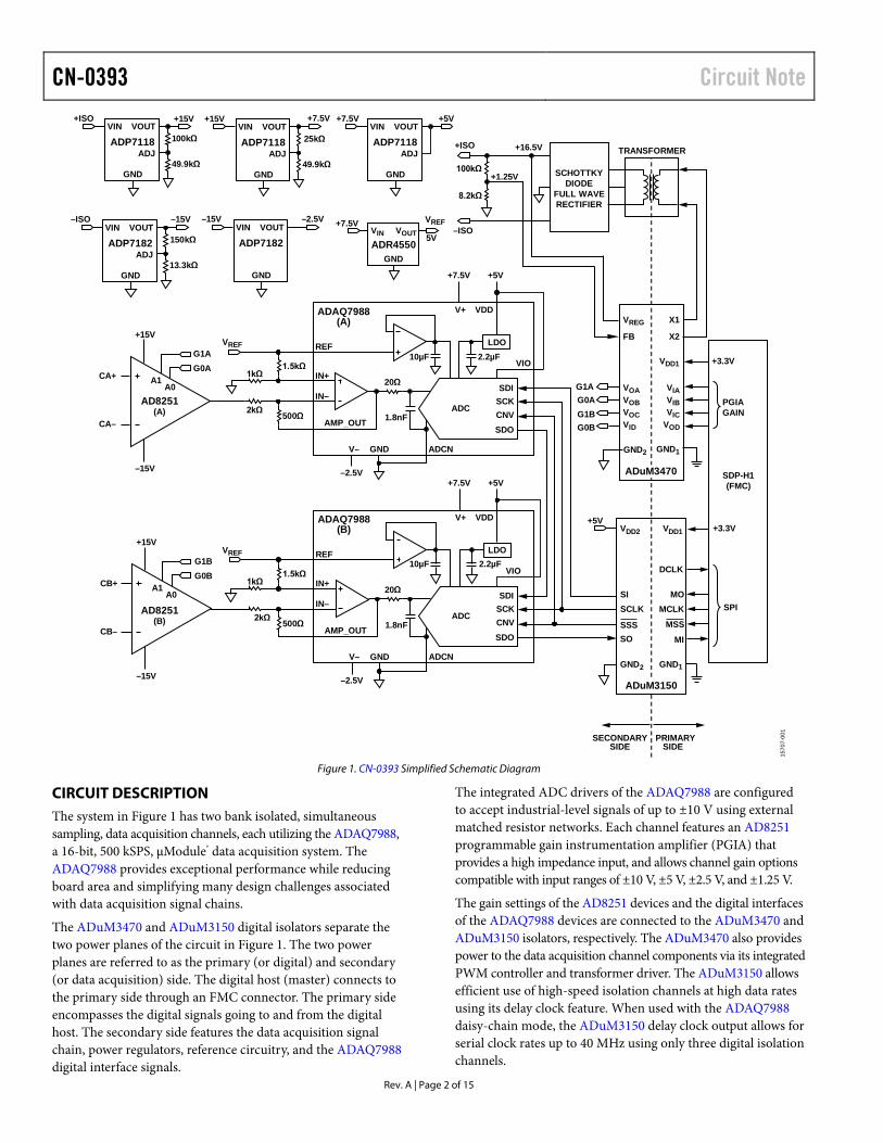
Figure 1. CN-0393 Simplified Schematic Diagram
CIRCUIT DESCRIPTION The system in Figure 1 has two bank isolated, simultaneous sampling, data acquisition channels, each utilizing the ADAQ7988, a 16-bit, 500 kSPS, μModule® data acquisition system. The ADAQ7988 provides exceptional performance while reducing board area and simplifying many design challenges associated with data acquisition signal chains.
The ADuM3470 and ADuM3150 digital isolators separate the two power planes of the circuit in Figure 1. The two power planes are referred to as the primary (or digital) and secondary (or data acquisition) side. The digital host (master) connects to the primary side through an FMC connector. The primary side encompasses the digital signals going to and from the digital host. The secondary side features the data acquisition signal chain, power regulators, reference circuitry, and the ADAQ7988 digital interface signals.
The integrated ADC drivers of the ADAQ7988 are configured to accept industrial-level signals of up to ±10 V using external matched resistor networks. Each channel features an AD8251 programmable gain instrumentation amplifier (PGIA) that provides a high impedance input, and allows channel gain options compatible with input ranges of ±10 V, ±5 V, ±2.5 V, and ±1.25 V.
The gain settings of the AD8251 devices and the digital interfaces of the ADAQ7988 devices are connected to the ADuM3470 and ADuM3150 isolators, respectively. The ADuM3470 also provides power to the data acquisition channel components via its integrated PWM controller and transformer driver. The ADuM3150 allows efficient use of high-speed isolation channels at high data rates using its delay clock feature. When used with the ADAQ7988 daisy-chain mode, the ADuM3150 delay clock output allows for serial clock rates up to 40 MHz using only three digital isolation channels.
Circuit Note CN-0393
Rev. A | Page 3 of 15
Evaluation software is provided to allow easy interfacing with the circuit shown in Figure 1. The software includes a graphical user interface (GUI) to control various circuit parameters and settings, which communicates to the FPGA on the SDP-H1 board. For more information on obtaining the software, see the Circuit Evaluation and Test section.
Component Selection
The ADAQ7988 is a 16-bit, 500 kSPS, μModule® data acquisition system that integrates four common signal processing and conditioning blocks into a system in package (SiP) design that supports a variety of applications. The ADAQ7988 also contains the most critical passive components, eliminating many of the design challenges associated with traditional signal chains that utilize successive approximation register (SAR) ADCs. These passive components are crucial to achieving the specified device performance.
The ADAQ7988 is part of an all Analog Devices, Inc., active component solution that contains a high accuracy, low power, 16-bit SAR ADC; a low power, high bandwidth ADC driver; a wideband noise RC filter; a low power, stable reference buffer; a 10 µF reference decoupling capacitor; and an efficient power management block, all housed in a tiny 5 mm × 4 mm LGA package. This integration reduces design complexity and can save up to 50% PCB area when compared to similar individual component designs. The ADAQ7988 also provides a significant level flexibility to adapt to a wide assortment of applications; for example, the integrated ADC driver can be set in a variety of configurations and gains, enabling compatibility with multiple input ranges.
The ADAQ7988 SPI-compatible serial interface features the ability to daisy-chain multiple devices on a single, 3-wire bus. This is ideal for isolated applications, as it limits the number of isolator channels required for communication between the device and the digital host.
The AD8251 is an instrumentation amplifier with digitally programmable gains. It features GΩ input impedance, low output noise, wide bandwidth (10 MHz) and low distortion. These qualities make the AD8251 an excellent candidate for wide bandwidth data acquisition applications. The high input impedance of the AD8251 enable it to interface with a variety of sensors, and provides an impedance translation between the input source and the ADC driver housed within the ADAQ7988. It can be configured for gains of 1, 2, 4, and 8 via its address pins, which are controlled by the digital host via the digital isolator channels of the ADuM3470.
The ADR4550 is a high precision, low power, low noise, 5 V voltage reference featuring ±0.02% maximum initial error, excellent temperature stability, and low output noise. The ADR4550 provides a 5 V reference to the integrated reference buffers of the two ADAQ7988 devices. The reference voltage is also divided by a precision resistor network to provide dc biasing (level shifting) to the ADC drivers of the ADAQ7988 devices.
The ADuM3470 is a quad-channel digital isolator with an integrated PWM controller and transformer driver for an isolated dc-to-dc converter. Based on the Analog Devices iCoupler® technology, the dc-to-dc converter provides up to 2 W of regulated, isolated power from 3.3 V to 24 V using a 3.3 V or 5.0 V input supply. This eliminates the need for a separate, isolated dc-to-dc converter in 2 W isolated designs. The iCoupler chip-scale transformer technology is used to isolate the logic signals, and the integrated transformer driver with isolated secondary side control provides higher efficiency for the isolated dc-to-dc converter. The rated dielectric insulation voltage of the ADuM3470 is 2500 V rms. The result is a small form factor, total isolation solution.
The ADuM3150 is a 6-channel SPIsolator™ digital isolator optimized for isolated serial peripheral interfaces (SPIs). Based on the Analog Devices iCoupler® chip scale transformer technology, the low propagation delay in the CLK, MO/SI, MI/SO, and SS SPI bus signals operate with 14 ns propagation delay and 1 ns jitter to optimize timing for SPI. The ADuM3150 also features a delay clock output on the master side of the device. This output can be used with an additional clocked port on the master to support 40 MHz clock performance. The rated dielectric insulation voltage of the ADuM3150 is 3750 V rms.
The power management on the secondary side of the system is handled by the ADP7118 and ADP7182 low dropout (LDO) linear regulators. A cascade of ADP7118 devices are used to regulate the positive rail provided by the ADuM3470 for the positive rails of the system. The ADP7182 devices on board do the same for the negative rails. See the Power Distribution section for more information.
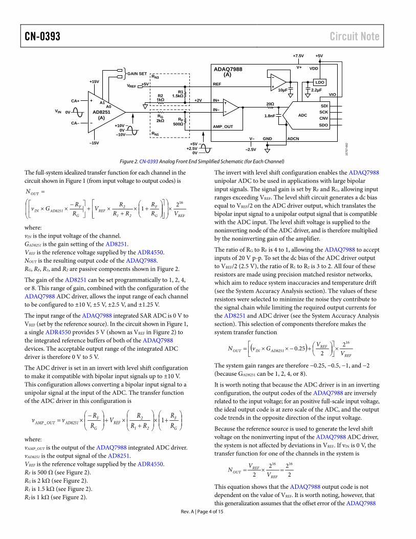
Analog Front End
The analog front end (AFE) of the system consists of input protection diodes, the AD8251 PGIA, the ADAQ7988 μModule® data acquisition system, and precision resistor networks used to configure the ADC driver of the ADAQ7988. The AFEs of both channels are identical in design, but their input ranges can be set independently by the gain settings of their respective AD8251. Figure 2 shows a simplified schematic of the AFE.
CN-0393 Circuit Note
Rev. A | Page 4 of 15
REF
GND
VDD
VIO
20Ω
V+
V–
1.8nF
LDO
2.2µF10µF
AMP_OUT
ADC
IN+
IN–
ADAQ7988
ADCN
SDISCK
SDOCNV
GAIN SET
AD8251(A)
+7.5V +5V
–2.5V
VREF+15V
–15V
CA+
CA–
(A)
A1A0
R11.5kΩ
RG2kΩ
R21kΩ
RF500Ω
RN3
RN1
+5V
+2V
0VVIN
0V+10V
–10V
+2.5V+5V
0V 1570
7-00
2
Figure 2. CN-0393 Analog Front End Simplified Schematic (for Each Channel)
The full-system idealized transfer function for each channel in the circuit shown in Figure 1 (from input voltage to output codes) is
REFG
F
21
2REF
G
FAD8251IN
OUT
VRR
RRR
VRR
Gv
N
1621 ×
+×
+×+
−××
=
where: vIN is the input voltage of the channel. GAD8251 is the gain setting of the AD8251. VREF is the reference voltage supplied by the ADR4550. NOUT is the resulting output code of the ADAQ7988. RG, RF, R1, and R2 are passive components shown in Figure 2.
The gain of the AD8251 can be set programmatically to 1, 2, 4, or 8. This range of gain, combined with the configuration of the ADAQ7988 ADC driver, allows the input range of each channel to be configured to ±10 V, ±5 V, ±2.5 V, and ±1.25 V.
The input range of the ADAQ7988 integrated SAR ADC is 0 V to VREF (set by the reference source). In the circuit shown in Figure 1, a single ADR4550 provides 5 V (shown as VREF in Figure 2) to the integrated reference buffers of both of the ADAQ7988 devices. The acceptable output range of the integrated ADC driver is therefore 0 V to 5 V.
The ADC driver is set in an invert with level shift configuration to make it compatible with bipolar input signals up to ±10 V. This configuration allows converting a bipolar input signal to a unipolar signal at the input of the ADC. The transfer function of the ADC driver in this configuration is
+×
+×+
−×=
G
F
21
2REF
G
FAD8251OUTAMP R
RRR
RV
RR
vv 1_
where: vAMP_OUT is the output of the ADAQ7988 integrated ADC driver. vAD8251 is the output signal of the AD8251. VREF is the reference voltage supplied by the ADR4550. RF is 500 Ω (see Figure 2). RG is 2 kΩ (see Figure 2). R1 is 1.5 kΩ (see Figure 2). R2 is 1 kΩ (see Figure 2).
The invert with level shift configuration enables the ADAQ7988 unipolar ADC to be used in applications with large bipolar input signals. The signal gain is set by RF and RG, allowing input ranges exceeding VREF. The level shift circuit generates a dc bias equal to VREF/2 on the ADC driver output, which translates the bipolar input signal to a unipolar output signal that is compatible with the ADC input. The level shift voltage is supplied to the noninverting node of the ADC driver, and is therefore multiplied by the noninverting gain of the amplifier.
The ratio of RG to RF is 4 to 1, allowing the ADAQ7988 to accept inputs of 20 V p-p. To set the dc bias of the ADC driver output to VREF/2 (2.5 V), the ratio of R1 to R2 is 3 to 2. All four of these resistors are made using precision matched resistor networks, which aim to reduce system inaccuracies and temperature drift (see the System Accuracy Analysis section). The values of these resistors were selected to minimize the noise they contribute to the signal chain while limiting the required output currents for the AD8251 and ADC driver (see the System Accuracy Analysis section). This selection of components therefore makes the system transfer function
( )REF
REFAD8251INOUT V
VGvN
1622
25.0 ×
+−××=
The system gain ranges are therefore −0.25, −0.5, −1, and −2 (because GAD8251 can be 1, 2, 4, or 8).
It is worth noting that because the ADC driver is in an inverting configuration, the output codes of the ADAQ7988 are inversely related to the input voltage; for an positive full-scale input voltage, the ideal output code is at zero scale of the ADC, and the output code trends in the opposite direction of the input voltage.
Because the reference source is used to generate the level shift voltage on the noninverting input of the ADAQ7988 ADC driver, the system is not affected by deviations in VREF. If vIN is 0 V, the transfer function for one of the channels in the system is
222
2
1616
=×=REF
REFOUT V
VN
This equation shows that the ADAQ7988 output code is not dependent on the value of VREF. It is worth noting, however, that this generalization assumes that the offset error of the ADAQ7988
Circuit Note CN-0393
Rev. A | Page 5 of 15
integrated reference buffer is negligible. This assumption is suitable because even with the maximum reference buffer offset specified for the ADAQ7988, the output code only deviates by less than one LSB (code value).
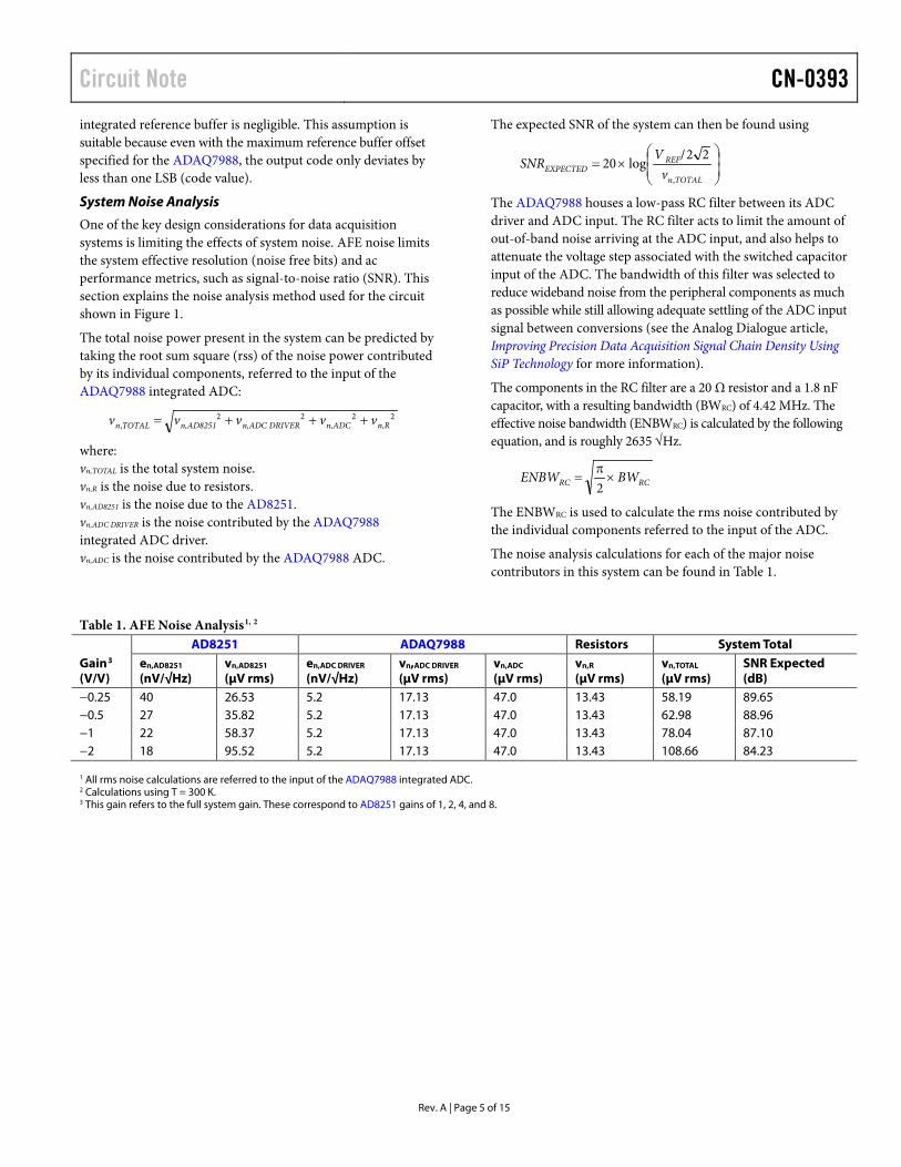
System Noise Analysis
One of the key design considerations for data acquisition systems is limiting the effects of system noise. AFE noise limits the system effective resolution (noise free bits) and ac performance metrics, such as signal-to-noise ratio (SNR). This section explains the noise analysis method used for the circuit shown in Figure 1.
The total noise power present in the system can be predicted by taking the root sum square (rss) of the noise power contributed by its individual components, referred to the input of the ADAQ7988 integrated ADC:
2222, n,Rn,ADCDRIVERn,ADCn,AD8251TOTALn vvvvv +++=
where: vn,TOTAL is the total system noise. vn,R is the noise due to resistors. vn,AD8251 is the noise due to the AD8251. vn,ADC DRIVER is the noise contributed by the ADAQ7988 integrated ADC driver. vn,ADC is the noise contributed by the ADAQ7988 ADC.
The expected SNR of the system can then be found using
×=
TOTALn
REFEXPECTED v
VSNR
,
22/log20
The ADAQ7988 houses a low-pass RC filter between its ADC driver and ADC input. The RC filter acts to limit the amount of out-of-band noise arriving at the ADC input, and also helps to attenuate the voltage step associated with the switched capacitor input of the ADC. The bandwidth of this filter was selected to reduce wideband noise from the peripheral components as much as possible while still allowing adequate settling of the ADC input signal between conversions (see the Analog Dialogue article, Improving Precision Data Acquisition Signal Chain Density Using SiP Technology for more information).
The components in the RC filter are a 20 Ω resistor and a 1.8 nF capacitor, with a resulting bandwidth (BWRC) of 4.42 MHz. The effective noise bandwidth (ENBWRC) is calculated by the following equation, and is roughly 2635 √Hz.
RCRC BWENBW ×π
=2
The ENBWRC is used to calculate the rms noise contributed by the individual components referred to the input of the ADC.
The noise analysis calculations for each of the major noise contributors in this system can be found in Table 1.
Table 1. AFE Noise Analysis1, 2
Gain3 (V/V)
AD8251 ADAQ7988 Resistors System Total en,AD8251 (nV/√Hz)
vn,AD8251 (µV rms)
en,ADC DRIVER (nV/√Hz)
vn,ADC DRIVER (µV rms)
vn,ADC (µV rms)
vn,R (µV rms)
vn,TOTAL (µV rms)
SNR Expected (dB)
−0.25 40 26.53 5.2 17.13 47.0 13.43 58.19 89.65 −0.5 27 35.82 5.2 17.13 47.0 13.43 62.98 88.96 −1 22 58.37 5.2 17.13 47.0 13.43 78.04 87.10 −2 18 95.52 5.2 17.13 47.0 13.43 108.66 84.23 1 All rms noise calculations are referred to the input of the ADAQ7988 integrated ADC. 2 Calculations using T = 300 K. 3 This gain refers to the full system gain. These correspond to AD8251 gains of 1, 2, 4, and 8.
CN-0393 Circuit Note
Rev. A | Page 6 of 15
Noise Contributed by AD8251
The rms noise contributed by the AD8251 is a function of its input-referred voltage noise (eAD8251), its gain setting (GAD8251), the signal gain of the ADAQ7988 ADC driver (set by RF and RG in Figure 2), and ENBWRC.
vn,AD8251 = eAD8251 × GAD8251 × (RF/RG) × ENBWRC
It is worth noting that eAD8251 is provided as the maximum specification and is different for each of its four gain settings. In practice, the noise contributed by the AD8251 is typically less than predicted using the voltage noise numbers from the AD8251 data sheet because the noise specifications of the AD8251 are statistically guardbanded.
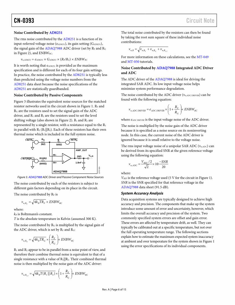
Noise Contributed by Passive Components
Figure 3 illustrates the equivalent noise sources for the matched resistor networks used in the circuit shown in Figure 1. RF and RG are the resistors used to set the signal gain of the ADC driver, and R1 and R2 are the resistors used to set the level shifting voltage (also shown in Figure 2). R1 and R2 are represented by a single resistor, with a resistance equal to the R1 in parallel with R2 (R1||R2). Each of these resistors has their own thermal noise which is included in the full system noise.
RG
R1||R2
RF
4kT(R||R12)
4kTRG 4kTRF
20Ω
1.8nF
Vn,R
ADAQ7988
IN+
IN–
AMP_OUT
. . .
2kΩ 500Ω
(600Ω)
1570
7-00
3
Figure 3. ADAQ7988 ADC Driver and Passive Component Noise Sources
The noise contributed by each of the resistors is subject to different gain factors depending on its place in the circuit.
The noise contributed by RF is
RCFBRn ENBWTRkvF
×= 4,
where: kB is Boltzmann’s constant. T is the absolute temperature in Kelvin (assumed 300 K).
The noise contributed by RG is multiplied by the signal gain of the ADC driver, which is set by RF and RG:
RCG
FGBRn ENBW
RR
TRkvG
×
×= 4,
R1 and R2 appear to be in parallel from a noise point of view, and therefore their combine thermal noise is equivalent to that of a single resistance with a value of R1||R2. Their combined thermal noise is then multiplied by the noise gain of the ADC driver:
RCG
F1BRn ENBW
RR
RRTkv1,2
×
+×= 1)||(4 2,
The total noise contributed by the resistors can then be found by taking the root sum square of these individual noise contributions:
21GF n,Rn,Rn,RRn vvvv,, ++=
For more information on these calculations, see the MT-049 and MT-050 tutorials.
Noise Contributed by ADAQ7988 Integrated ADC Driver and ADC
The ADC driver of the ADAQ7988 is ideal for driving the integrated SAR ADC. Its low input voltage noise helps minimize system performance degradation.
The noise contributed by the ADC driver (vn,ADC DRIVER) can be found with the following equation:
RCG
FDRIVERADCDRIVERADCn ENBW
RR
ev ×
+×= 1,
where eADC DRIVER is the input voltage noise of the ADC driver.
The noise is multiplied by the noise gain of the ADC driver because it is specified as a noise source on its noninverting node. In this case, the current noise of the ADC driver is ignored because it is small relative to the voltage noise.
The rms input voltage noise of a unipolar SAR ADC (vn,ADC) can be derived from its specified SNR at the given reference voltage using the following equation:
2010
22/
,SNRV
v REFADCn
−×=
where: VREF is the reference voltage used (5 V for the circuit in Figure 1). SNR is the SNR specified for that reference voltage in the ADAQ7988 data sheet (91.5 dB).
System Accuracy Analysis
Data acquisition systems are typically designed to achieve high accuracy and precision. The components that make up the system introduce some amount of error and uncertainty, however, which limits the overall accuracy and precision of the system. Two commonly specified system errors are offset and gain error. These errors are affected by temperature drift, as well. They can typically be calibrated out at a specific temperature, but not over the full operating temperature range. The following sections explain how to estimate the maximum expected system inaccuracy at ambient and over temperature for the system shown in Figure 1 using the error specifications of its individual components.
Circuit Note CN-0393
Rev. A | Page 7 of 15
Offset Error Analysis
Offset error is a system inaccuracy that is independent of the input signal. The sources of offset error in this system include the offset of the AD8251 (VOS,AD8251), the zero error of the ADAQ7988 (VOS,ADAQ7988), the offset caused by the input bias currents of the ADC driver (VOS,IB), and the inaccuracy in the generation of the level shifting voltage on the noninverting node of the ADC driver (VOS,LS). The maximum expected system offset error (referred to input) can be found by adding these together:
VOS,SYSTEM = VOS,AD8251 + VOS,LS + VOS,ADAQ7988 + VOS,IB
Table 2 shows the calculation of the maximum expected referred to input (RTI) system offset error. To convert the offsets of the components to the system offset, they must be multiplied or divided by the relevant gain factors, that is, the noninverting and inverting gains of the ADC driver and the gain settings of the AD8251. The nominal non-inverting and inverting gains of the ADC driver are 1.25 and 0.25, respectively, and these numbers are used to calculate system RTI offset.
The maximum input referred offset of the AD8251 is specified as a function of its gain setting. Table 2 shows the RTI offset error of the AD8251 for all four of its gain settings. See the AD8251 data sheet for more information.
The zero error of the ADAQ7988 specifies the total input referred offset error, and can be treated as an input voltage offset error at the input to its integrated ADC driver. The maximum zero error of the ADAQ7988 is specified as ±0.5 mV. This error can be converted to system RTI offset error by multiplying it by the ADC driver noninverting gain (1.25) and dividing it by the ADC driver inverting gain (−0.25) and AD8251 gain:
)mV()25.0(
)25.1(5.0,
AD8251ADAQ7988OS G
V×−
×±=
or
)mV(5.2,
AD8251ADAQ7988OS G
V ±=
where GAD8251 is the gain setting of the AD8251.
The input bias currents of the ADC driver create an offset error when they interact with the matched resistor networks at its inputs. The output referred offset this creates can be found with
VOS,IB(RTO) = IB × [RF − (R1||R2)(1.25)]
or
VOS,IB(RTO) = −0.2 mV
where IB is the input bias current specification for the ADAQ7988 integrated ADC driver (800 nA maximum).
In this case, the bias currents were assumed to be equal, because the input offset current of the device is considerably small compared to its input bias current. (See the MT-038 tutorial for more information on input bias current errors.)
To convert the output referred offset caused by the input bias currents (VOS,IB(RTO)) to system input referred offset error, it is divided by the inverting gain of the ADC driver and the gain of the AD8251:
)mV(8.0)mV(25.0
2.0,
AD8251AD8251IBOS GG
V =×−−
=
This offset error is always positive referred to input; therefore, it is used for calculating the maximum positive offset error, but is ignored for calculating the maximum negative offset error.
Inaccuracies in the generation of the level shift voltage in the ADC driver also introduce offset errors to the system; however, because the level shift voltage is provided by the reference source of the ADC, the system offset is not sensitive to deviations in the reference voltage (see the Analog Front End section), which means that the only error source for the level shift voltage is the tolerance of the resistors in the divider circuit consisting of R1 and R2. The ideal level shift voltage at the noninverting input of the ADAQ7988 integrated ADC driver can be found with the following equation:
(nominal)4.0, REF21
2REFNOMINALLS V
RRR
VV ×=+
×=
The resistor divider is constructed of a matched resistor network and is shown R1 and R2 in Figure 2. The network contains four 1 kΩ resistors that are configured to create an attenuation factor of 0.4 (R1 = 1.5 kΩ, R2 = 1 kΩ). The resistors in the network are specified with a relative tolerance of ±0.05%, which helps to reduce the deviation from the 0.4 attenuation. The worst-case error of the divider circuit, given the configuration and relative tolerance of the matched resistor network used, is ±0.03%. (The resistor networks used for generating the level shift voltage can be found in the CN-0393 schematic, in the CN-0393 Design Support Package.)
The range of the level shift voltage at the noninverting input of the ADAQ7988 integrated ADC driver is, therefore,
VLS = 5 V × (0.4 ± 0.03%) = 2 V ± 0.6 mV
Referred to the input of the system, the offset error contributed by the level shift inaccuracy is
AD8251AD8251LSOS GG
VmV3
25.025.1mV6.0
,±
=×−
×±=
The maximum expected input referred offset error for the system in Figure 1 is then the sum of these errors. Table 2 shows the calculations for all four channel gain configurations. Note that these are the maximum expected errors at ambient temperature (25°C).
CN-0393 Circuit Note
Rev. A | Page 8 of 15
Table 2. Maximum Expected RTI System Offset Error
Channel Gain VOS,AD8251 (mV) VOS,LS (mV) VOS,ADAQ7988 (mV) VOS,IB (mV) VOS,SYSTEM (mV)
Min Max −0.25 ±0.8 ±3 ±2.5 +0.8 −6.3 +7.1 −0.5 ±0.5 ±1.5 ±1.25 +0.4 −3.25 +3.65 −1 ±0.35 ±0.75 ±0.625 +0.2 −1.725 +1.925 −2 ±0.275 ±0.375 ±0.3125 +0.1 −0.9715 +1.0715
Offset Error Temperature Drift
System calibration routines can correct for the ambient offset error of the system, but typically not error variations due to temperature drift. Quantifying how the offset changes for temperature variations is useful for evaluating how the system operates over a specified temperature range. Each of the active components in the signal chain have specified temperature drifts for their offsets. The resistor networks also have a relative temperature coefficient specification that guarantees the relative matching of the variation of each resistor over temperature.
The temperature drift of the offset error can be treated as a system specification by combining the temperature drift effects of each of the individual components, assuming there is no temperature variation between the components in the signal chain. Assuming all devices are at equal temperature and that their drifts all trend in the same direction, the maximum expected system offset temperature drift is
TCVOS,SYSTEM = TCVOS,AD8251 + TCBOS,LS + TCVOS,ADAQ7988
where: TCVOS,AD8251 is the input-referred offset drift of the AD8251 over its specified temperature range (in µV/°C). TCVOS,LS is the temperature drift of the level shift voltage supplied to the ADAQ7988 integrated ADC driver (referred to the input of the AD8251, in µV/°C). TCVOS,ADAQ7988 is the offset drift of the ADAQ7988 (referred to the input of AD8251, in µV/°C). TCVOS,SYSTEM is the equivalent input-referred offset temperature drift of each channel in the circuit shown in Figure 1.
The AD8251 input referred offset drift (TCVOS,AD8251) is given in its data sheet for all four of its gain settings; these values are shown in Table 3.
The ADAQ7988 zero error temperature drift is also provided in its data sheet, with a specified maximum of 1.3 µV/°C. This drift can be converted to system RTI temperature drift with the same method used to convert its ambient offset error (see the Offset Error Analysis section):
)μV/°C()25.0(
)25.1(3.1,
AD8251ADAQ7988OS G
TCV×−×±
=
or
)μV/°C(5.6,
AD8251ADAQ7988OS G
TCV ±=
where GAD8251 is the gain setting of the AD8251.
The temperature drift of the level shift voltage is due to the temperature drift of the resistor divider composed of R1 and R2. The offset drift of the reference source is negated by the system because it is shared by the level shift voltage and the ADAQ7988 integrated ADC (see the Analog Front End section). The temperature drift of the level shift voltage is therefore determined by the drift of R1 and R2, and
)4.0()()(
DIVREF
2211
22REF
LSLS
TCRVTCRRTCRR
TCRRV
TCVV
±×=
±±
±×=
±
where: VLS is the nominal level shift voltage (nominally 2 V). TCVLS is the equivalent temperature drift of the level shift voltage (in µV/°C). VREF is the reference voltage supplied by the ADR4550 (nominally 5 V). TCR1 and TCR2 are the temperature coefficients of R1 and R2, respectively (in ppm/°C). TCRDIV is the equivalent temperature drift of the resistor divider (in ppm/°C). TCRDIV is the deviation of the divider ratio, which is nominally 0.4 (see the Analog Front End section).
The resistors in the matched resistor network have a specified maximum relative temperature coefficient of resistance (TCR) of ±15 ppm. To determine the effective temperature drift of the level shift voltage, R2 is assumed to have no temperature drift, and the components comprising R1 are assumed to have an absolute TCR of ±15 ppm (TCR1 = 15 ppm/°C and TCR2 = 0 ppm/°C). This scenario exhibits the worst-case error of the resistor divider. The maximum expected temperature drift of the resistor divider is, therefore,
4.0kΩ1C)ppm/15kΩ(1.5
kΩ1, −
+°±=MAXDIVTCR
TCRDIV,MAX is equivalent to ±9 ppm/°C.
The temperature drift of the level shift voltage is, therefore,
VLS ± TCVLS = VREF × (0.4 ± 9 ppm/°C) = 2 V ± 9 ppm/°C
Because TCVLS is in ppm/°C, it can be directly applied to the input of the AD8251; TCVOS,LS is ±9 ppm/°C at the input of the AD8251, or
AD8251LSOS G
TCVCμV/90
,
°±=
Circuit Note CN-0393
Rev. A | Page 9 of 15
The maximum expected offset temperature drift for the system shown in Figure 1 is the sum of the temperature drifts for the individual components. Table 3 shows the calculations for all four channel gain configurations.
Table 3. Maximum Expected System Offset Temperature Drift Channel Gain
TCVOS,AD8251 (µV/°C)
TCVOS,LS (µV/°C)
TCVOS,ADAQ7988 (µV/°C)
TCVOS,SYSTEM (µV/°C)
−0.25 ±6.2 ±90 ±6.5 ±102.7 −0.5 ±3.7 ±45 ±3.25 ±51.95 −1 ±2.45 ±22.5 ±1.63 ±26.58 −2 ±1.83 ±11.25 ±0.82 ±13.9
Gain Error Analysis
Gain error is a system inaccuracy that scales with the input signal. The sources of gain error include the gain errors of the AD8251 and ADAQ7988, the errors in the signal gain of the ADC driver caused by the tolerances of the gain setting resistors, and the error of the reference voltage source (ADR4550). The nominal gain of a channel in the circuit shown in Figure 1 is
)codes/V(8.3276
)codes/V(216,
AD8251
REFG
FAD8251
IDEALSYSTEM
G
VRR
G
G
−=
×−
×=
where: GAD8251 is the gain setting of the AD8251. VREF is the reference voltage supplied by the ADR4550. RF and RG are the resistors used to set the gain of the ADAQ7988 integrated ADC driver (shown in Figure 2).
The worst-case range of the system can be found by adding the individual component gain errors, as follows:
( )
( ) )codes/V(1216
±×
±
×
±
−×±=
ADAQ7988REFREF
GG
FAD8251AD8251SYSTEM
eeV
eRR
eGG
where: GSYSTEM is the full system gain (the gain of each channel). eAD8251 is the AD8251 gain error (for each of its gain settings). eG is the error in the ratio of RF and RG. eREF is the reference voltage error. eADAQ7988 is the ADAQ7988 gain error.
The maximum expected system gain error (eSYSTEM) is the sum of each of the individual maximum expected gain errors of each of the components in the signal chain:
eSYSTEM = eAD8251 + eG + eREF + eADAQ7988
Table 4 shows the calculation of the maximum expected system gain error for each of the four channel gain configurations.
The AD8251 specifies a maximum gain error for each of its four gain configurations. These gain errors are shown in the eAD8251 column in Table 4. The ADAQ7988 also specifies a maximum gain error in percent full scale, also shown in Table 4.
The maximum signal gain error of the ADAQ7988 integrated ADC driver can be calculated based on the relative tolerance errors of the gain setting resistors in the matched resistor network (RF and RG in Figure 2). Like the networks used in setting the level shifting voltage, this network contains four 1 kΩ resistors. These resistors are configured to create an RF of 500 Ω and RG of 2 kΩ, with a resulting nominal gain of −0.25 (see the CN-0393 schematic). The resistors in the network are specified with a relative tolerance of ±0.05%, and the resulting maximum deviation of the signal gain is also roughly ±0.05%.
Though deviations in the reference source do not impact system offset error, it does affect the system gain error. Major errors in the reference source include initial output voltage error (±0.02% or ±1 mV), solder heat shift (±0.02% or ±1 mV), and inaccuracies caused by load regulation limitations (80 ppm/mA). These specifications can be found in the ADR4550 data sheet. In the circuit shown in Figure 1, the ADR4550 is directly connected to the matched resistor networks making the level shift voltage for both channels. Each of these networks acts as a 2.5 kΩ load; therefore, the ADR4550 sources a total of 4 mA, which means its worst-case load regulation error is 320 ppm, or ±1.6 mV. The total maximum error in the reference voltage is the sum of these three errors, which is ±3.6 mV or ±0.072%.
The total maximum expected system gain error for the system in Figure 1 can be found using these individual component errors. Table 4 shows the maximum expected system gain error for all four channel gain configurations. Note that these values are the maximum expected errors at ambient temperature (25°C).
Table 4. Maximum Expected System Gain Error Channel Gain eAD8251 eG eREF eADAQ7988 eSYSTEM −0.25 ±0.03% ±0.05% ±0.072% ±0.01% ±0.162% −0.5 ±0.04% ±0.05% ±0.072% ±0.01% ±0.172% −1 ±0.04% ±0.05% ±0.072% ±0.01% ±0.172% −2 ±0.04% ±0.05% ±0.072% ±0.01% ±0.172%
Gain Error Temperature Drift
The system gain error is also subject to variations in temperature. Like with offset error drift, it is important to quantify the gain temperature drift because these variations typically cannot be corrected for with calibration. Each of the active components in the signal chain have specified temperature drifts for their gains. The resistor networks also have a relative temperature coefficient specification that guarantees the relative matching of the variation of each resistor over temperature.
The temperature variation of the system gain is a function of the temperature drift specifications of individual component. Like with the ambient system gain error, the maximum expected
CN-0393 Circuit Note
Rev. A | Page 10 of 15
system gain temperature drift is the sum of component gain temperature drifts:
TCSYSTEM = TCAD8251 + TCG + TCREF + TCADAQ7988
where: TCSYSTEM is the maximum expected system gain temperature drift. TCAD8251 is the gain temperature drift specification of the AD8251. TCG is the gain temperature drift of the closed-loop gain of the ADAQ7988 integrated ADC driver (a function of the temperature drift of RF and RG). TCREF is the temperature drift specification of the ADR4550. TCADAQ7988 is the gain error temperature drift specification for the ADAQ7988.
TCAD8251, TCREF, and TCADAQ7988 can be found in the AD8251, ADR4550, and ADAQ7988 data sheets. TCAD8251 is 10 ppm/°C (for all AD8251 gain settings), TCREF is 2 ppm/°C, and TCADAQ7988 is 0.4 ppm/°C.
TCG is dependent upon the relative TCR of the matched resistor network that comprises Rf and Rg. As discussed in the Offset Error Temperature Drift section, these resistors have a relative TCR matching of 15 ppm/°C. Because the ADC driver closed-loop gain is the ratio of RF to RG, the temperature drift of the closed-loop gain is equivalent to this relative TCR matching specification; therefore, TCG is 15 ppm/°C.
TCSYSTEM is then
TCSYSTEM = ±10 ppm/°C ± 15 ppm/°C ± 2 ppm/°C ± 0.4 ppm/°C = ±27.4 ppm/°C
Digital Interface and Isolation
The system shown in Figure 1 features isolation between the digital host and data acquisition signal chain. The ADuM3470 and ADuM3150 provide digital isolation channels for the AD8251 address signals and the ADAQ7988 SPI signals, respectively.
A key design consideration for digital isolation applications is efficient usage of isolation channels; that is, optimizing the number of isolation channels used to accomplish a design. This is because additional isolation channels may require the addition of new components, which adds to design cost, circuit area, and power consumption. The digital implementation of this system achieves this efficiency by not only optimizing the routing of the ADAQ7988 SPI signals across the isolation barrier, but by including power distribution circuitry in the isolator device controlling the AD8251 address signals.
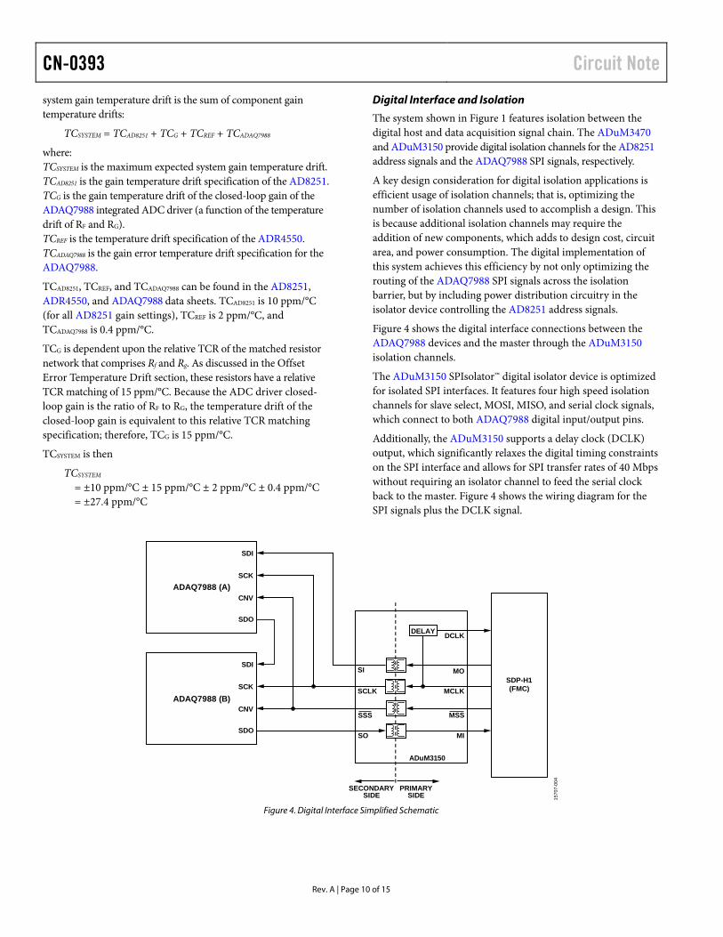
Figure 4 shows the digital interface connections between the ADAQ7988 devices and the master through the ADuM3150 isolation channels.
The ADuM3150 SPIsolator™ digital isolator device is optimized for isolated SPI interfaces. It features four high speed isolation channels for slave select, MOSI, MISO, and serial clock signals, which connect to both ADAQ7988 digital input/output pins.
Additionally, the ADuM3150 supports a delay clock (DCLK) output, which significantly relaxes the digital timing constraints on the SPI interface and allows for SPI transfer rates of 40 Mbps without requiring an isolator channel to feed the serial clock back to the master. Figure 4 shows the wiring diagram for the SPI signals plus the DCLK signal.
ADuM3150
SO
SSS
SCLK
SI
MI
MSS
MCLK
MO
DCLK
ADAQ7988 (A)
SDO
CNV
SCK
SDI
SDP-H1(FMC)
DELAY
ADAQ7988 (B)
SDO
CNV
SCK
SDI
SECONDARYSIDE
PRIMARYSIDE 15
707-
004
Figure 4. Digital Interface Simplified Schematic
Circuit Note CN-0393
Rev. A | Page 11 of 15
The DCLK signal is a delayed reproduction of the serial clock provided by the master (MCLK). The delay between MCLK and DCLK is trimmed at production test to match the roundtrip propagation delay of the serial clock and MISO channels of the ADuM3150. The DCLK can be used as an independent read clock by the master to clock in the data on the MISO line. This configuration ensures that MISO data are ready when they are clocked in with DCLK. See the MS-2689 Technical Article, Isolating SPI for High Bandwidth Sensors for more information.
The ADAQ7988 devices in the design are configured in daisy-chain mode. This configuration allows for the 16-bit results of both ADAQ7988 devices to be transmitted along a single MISO (SDO) line, thus requiring only a single isolator channel to transmit the data back to the master. The conversion results from both devices are clocked out by falling edges on their SCK pins, analogous to two serially connected 16-bit shift registers. This arrangement requires the master to output 32 serial clock cycles to read both results.
For information on layout design using the digital isolators, consult the ADuM3470 and ADuM3150 data sheets.
Power Distribution
In addition to providing isolation channels for the AD8251 addresses, the ADuM3470 supplies power from the primary side to the secondary side of the circuit shown in Figure 1. The ADuM3470 features integrated PWM controllers and low impedance transformer drivers (X1 and X2), which drive an external transformer, full-wave Schottky diode rectifier, and low-pass filter. The power circuit provides up to 2 W of regulated, isolated power when supplied from a 5 V or 3.3 V input, thereby eliminating the need for a separate isolated dc-to-dc converter.
The ADuM3470 regulation is from the positive supply. The feedback for regulation is from a divider network chosen such that the feedback voltage is 1.25 V when the output voltage is roughly 16.5 V. The feedback voltage is compared with the ADuM3470 internal feedback set point of 1.25 V. Regulation is achieved by varying the duty cycle of the PWM signal driving the external transformer.
The positive and negative power outputs of the transformer are regulated by several ADP7118 and ADP7182 low dropout (LDO) regulators. Table 5 shows the rails provided on the secondary side.
Table 5. Supply Rails on Secondary Side Rail Name Voltage Function Device Used +VS +15 V AD8251 positive rail ADP7118 V+ +7.5 V ADAQ7988 ADC driver
positive rail ADP7118
VDD +5 V ADAQ7988 LDO input supply
ADP7118
−VS −15 V AD8251 negative rail ADP7182 V− −2.5 V ADAQ7988 ADC driver
negative rail ADP7182
Performance Measurements
AC Performance Results
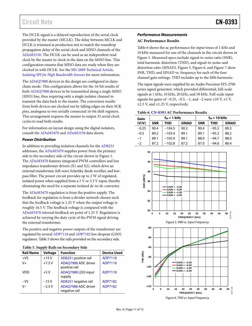
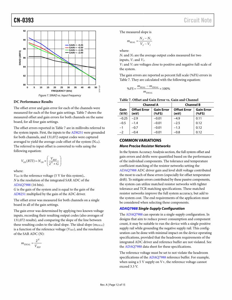
Table 6 shows the ac performance for input tones of 1 kHz and 10 kHz measured for one of the channels in the circuit shown in Figure 1. Measured specs include signal-to-noise ratio (SNR), total harmonic distortion (THD), and signal-to-noise-and distortion ratio (SINAD). Figure 5, Figure 6, and Figure 7 show SNR, THD, and SINAD vs. frequency for each of the four channel gain settings. THD includes up to the fifth harmonic.
The input signals were supplied by an Audio Precision SYS-2700 series signal generator, which provided differential, full-scale signals at 1 kHz, 10 kHz, 20 kHz, and 50 kHz. Full-scale input signals for gains of −0.25, −0.5, −1, and −2 were ±10 V, ±5 V, ±2.5 V, and ±1.25 V, respectively.
Table 6. CN-0393 AC Performance Results
Gain (V/V)
fIN = 1 kHz fIN = 10 kHz SNR THD SINAD SNR THD SINAD
−0.25 90.4 −104.5 90.3 90.4 −95.5 89.3 −0.5 89.2 −103.4 89.1 89.1 −95.2 88.2 −1 89.1 −105.9 89.1 88.9 −94.7 88.0 −2 87.2 −102.8 87.2 87.0 −94.6 86.4
80
82
84
86
88
90
92
0 5 10 15 20 25 30 35 40 45 50
SNR
(dBF
S)
FREQUENCY (kHz)
GAIN = –0.25GAIN = –0.50GAIN = –1.00GAIN = –2.00
1570
7-10
5
Figure 5. SNR vs. Input Frequency
–110
–105
–100
–95
–90
–85
–80
0 5 10 15 20 25 30 35 40 45 50
THD
(dB
c)
FREQUENCY (kHz)
GAIN = –0.25GAIN = –0.50GAIN = –1.00GAIN = –2.00
1570
7-10
6
Figure 6. THD vs. Input Frequency
CN-0393 Circuit Note
Rev. A | Page 12 of 15
80
82
84
86
88
90
92
0 5 10 15 20 25 30 35 40 45 50
SINA
D(d
BFS)
FREQUENCY (kHz)
GAIN = –0.25GAIN = –0.50GAIN = –1.00GAIN = –2.00
1570
7-10
7
Figure 7. SINAD vs. Input Frequency
DC Performance Results
The offset error and gain error for each of the channels were measured for each of the four gain settings. Table 7 shows the measured offset and gain errors for both channels on the same board, for all four gain settings.
The offset errors reported in Table 7 are in millivolts referred to the system inputs. First, the inputs to the AD8251 were grounded for both channels, and 131,072 output codes were captured averaged to yield the average code offset of the system (NOS). The referred to input offset is converted to volts using the following equation:
××=
GV
NRTIV NREF
OSOS 2)(
where: VREF is the reference voltage (5 V for this system),. N is the resolution of the integrated SAR ADC of the ADAQ7988 (16 bits). G is the gain of the system and is equal to the gain of the AD8251 multiplied by the gain of the ADC driver.
The offset error was measured for both channels on a single board in all of the gain settings.
The gain error was determined by applying two known voltage inputs, recording their resulting output codes (also averages of 131,072 results), and comparing the slope of the line between these resulting codes to the ideal slope. The ideal slope (mIDEAL) is a function of the reference voltage (VREF), and the resolution of the SAR ADC (N):
REF
N
IDEAL Vm 2
=
The measured slope is
12
12REAL VV
NNm
−
−=
where: N1 and N2 are the average output codes measured for two inputs, V1 and V2. V1 and V2 are voltages close to positive and negative full-scale of the system.
The gain errors are reported as percent full scale (%FS) errors in Table 7. They are calculated with the following equation:
%100% ×−
=IDEAL
IDEALREAL
mmm
FS
Table 7. Offset and Gain Error vs. Gain and Channel
Gain (V/V)
Channel A Channel B Offset Error (mV)
Gain Error (%FS)
Offset Error (mV)
Gain Error (%FS)
−0.25 −2.9 −0.01 −4.9 0.11 −0.5 −1.4 −0.01 −2.5 0.12 −1 −0.7 −0.01 −1.3 0.12 −2 −0.4 −0.01 −0.8 0.12
COMMON VARIATIONS More Precise Resistor Networks
In the System Accuracy Analysis section, the full system offset and gain errors and drifts were quantified based on the performance of the individual components. The tolerance and temperature coefficient matching of the resistor networks setting the ADAQ7988 ADC driver gain and level shift voltage contributed the most to each of these errors (especially for offset temperature drift). To mitigate errors contributed by these passive components, the system can utilize matched resistor networks with tighter tolerance and TCR matching specifications. These matched resistor networks improve the full system accuracy, but add to the system cost. The end requirements of the application must be considered when selecting these components.
ADAQ7988 Single-Supply Configuration
The ADAQ7988 can operate in a single-supply configuration. In designs that aim to reduce power consumption and component count, it may be suitable to run the device with a single positive supply rail while grounding the negative supply rail. This config-uration can be done with minimal impact on the device operating specifications, provided that the headroom requirements of the integrated ADC driver and reference buffer are not violated. See the ADAQ7988 data sheet for these specifications.
The reference voltage must be set to not violate the headroom specifications of the ADAQ7988 reference buffer. For example, when using a 5 V supply on V+, the reference voltage cannot exceed 3.3 V.
Circuit Note CN-0393
Rev. A | Page 13 of 15
Additional Circuit Protection
The circuit shown in Figure 1 has several means of overvoltage protection. TVS protection diodes are included at both inputs of both channels to protect them from large transient voltage spikes. The ADAQ7988 design is also robust enough to handle an overvoltage event where the output of the AD8251 overranges; the ESD diodes of the ADC, the integrated 20 Ω resistor, and the short-circuit current limitations of the integrated reference buffer and ADC driver prevent damage to the device (see the ADAQ7988 data sheet for more information). Figure 8 shows the connections of the internal ESD diodes of the ADC.
REF_OUT
GND
REF
ADCN
AMP_OUT
20Ω
1.8nFIN+
IN–
ADAQ7988
1570
7-00
5
Figure 8. ADC Input ESD Diodes
If the ADAQ7988 integrated ADC driver exceeds the reference voltage, the ESD diode connecting the ADC input to REF_OUT turns on. The current going through the diode depends on the voltage at AMP_OUT and REF_OUT, as well as the 20 Ω series resistor. In typical SAR ADC designs, care must be taken to make sure that the current going through the ESD diode does not cause the reference source to deviate, especially if the source is shared between multiple devices; however, the short-circuit current limitations for the two amplifiers ensures that the reference buffer is able to sink the current from the ADC driver without deviating.
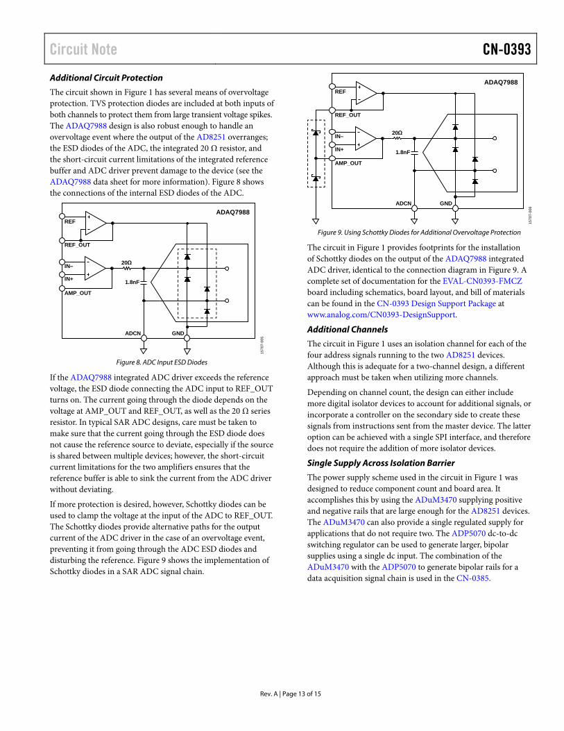
If more protection is desired, however, Schottky diodes can be used to clamp the voltage at the input of the ADC to REF_OUT. The Schottky diodes provide alternative paths for the output current of the ADC driver in the case of an overvoltage event, preventing it from going through the ADC ESD diodes and disturbing the reference. Figure 9 shows the implementation of Schottky diodes in a SAR ADC signal chain.
REF_OUT
GND
REF
ADCN
AMP_OUT
20Ω
1.8nFIN+
IN–
ADAQ7988
1570
7-00
6
Figure 9. Using Schottky Diodes for Additional Overvoltage Protection
The circuit in Figure 1 provides footprints for the installation of Schottky diodes on the output of the ADAQ7988 integrated ADC driver, identical to the connection diagram in Figure 9. A complete set of documentation for the EVAL-CN0393-FMCZ board including schematics, board layout, and bill of materials can be found in the CN-0393 Design Support Package at www.analog.com/CN0393-DesignSupport.
Additional Channels
The circuit in Figure 1 uses an isolation channel for each of the four address signals running to the two AD8251 devices. Although this is adequate for a two-channel design, a different approach must be taken when utilizing more channels.
Depending on channel count, the design can either include more digital isolator devices to account for additional signals, or incorporate a controller on the secondary side to create these signals from instructions sent from the master device. The latter option can be achieved with a single SPI interface, and therefore does not require the addition of more isolator devices.
Single Supply Across Isolation Barrier
The power supply scheme used in the circuit in Figure 1 was designed to reduce component count and board area. It accomplishes this by using the ADuM3470 supplying positive and negative rails that are large enough for the AD8251 devices. The ADuM3470 can also provide a single regulated supply for applications that do not require two. The ADP5070 dc-to-dc switching regulator can be used to generate larger, bipolar supplies using a single dc input. The combination of the ADuM3470 with the ADP5070 to generate bipolar rails for a data acquisition signal chain is used in the CN-0385.
CN-0393 Circuit Note
Rev. A | Page 14 of 15
CIRCUIT EVALUATION AND TEST This circuit uses the EVAL-CN0393-FMCZ circuit board and the SDP-H1 system demonstration platform controller board (EVAL-SDP-CH1Z). The two boards connect via a 160-pin FMC connector, allowing quick setup and evaluation of the performance of the circuit. The EVAL-CN0393-FMCZ board contains the circuit shown in Figure 1, and the SDP-H1 board interfaces with the CN-0393 Evaluation Software to operate this circuit.
Equipment Needed
The following equipment is needed:
PC with a USB port and Windows® XP, Windows Vista®, or Windows 7®
EVAL-CN0393-FMCZ circuit evaluation board SDP-H1 controller board (EVAL-SDP-CH1Z) CN-0393 Evaluation Software (download from
ftp://ftp.analog.com/pub/cftl/CN0393/) 12 V dc switched mode power supply USB to micro-USB cable Low distortion, low noise signal generator to provide
±10 V input signals Low noise, high precision dc supply to provide ±10 V input
Software Installation
Load the evaluation software by first downloading it from ftp://ftp.analog.com/pub/cftl/CN0393/, and then installing it on the PC. The CN-0393 User Guide has instructions for installing and running this software.
Setup and Test
Do not connect power to the hardware until both the EVAL-CN0393-FMCZ and SDP-H1 boards are connected via the 160-pin FMC connector. To set up the EVAL-CN0393-FMCZ and SDP-H1 hardware, take the following steps:
1. Connect the EVAL-CN0393-FMCZ and the SDP-H1 via the 160-pin FMC connector.
2. Connect the 12 V dc switched-mode power supply to the +12V_VIN jack on the SDP-H1 board. Note that power is not provided to the EVAL-CN0393-FMCZ board until the CN-0393 Evaluation Software has initialized.
3. Connect the SDP-H1 board to the PC via the USB cable. 4. Run the CN-0393 Evaluation Software (see the CN-0393
User Guide for instructions).
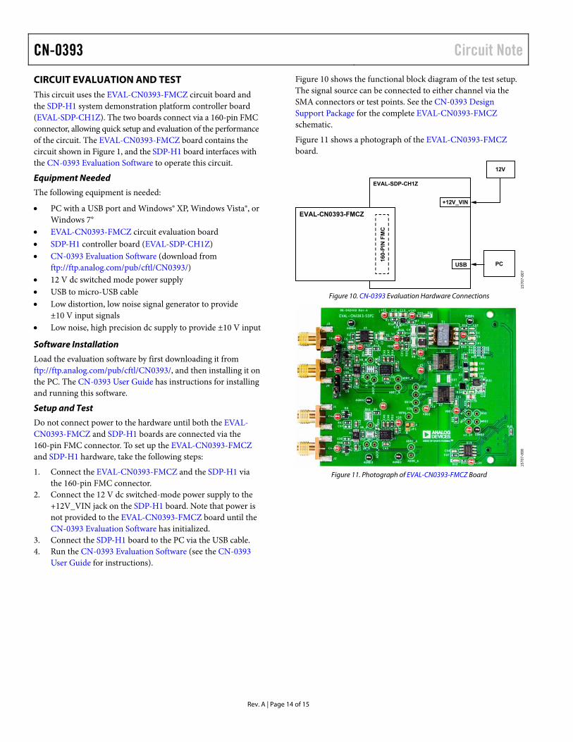
Figure 10 shows the functional block diagram of the test setup. The signal source can be connected to either channel via the SMA connectors or test points. See the CN-0393 Design Support Package for the complete EVAL-CN0393-FMCZ schematic.
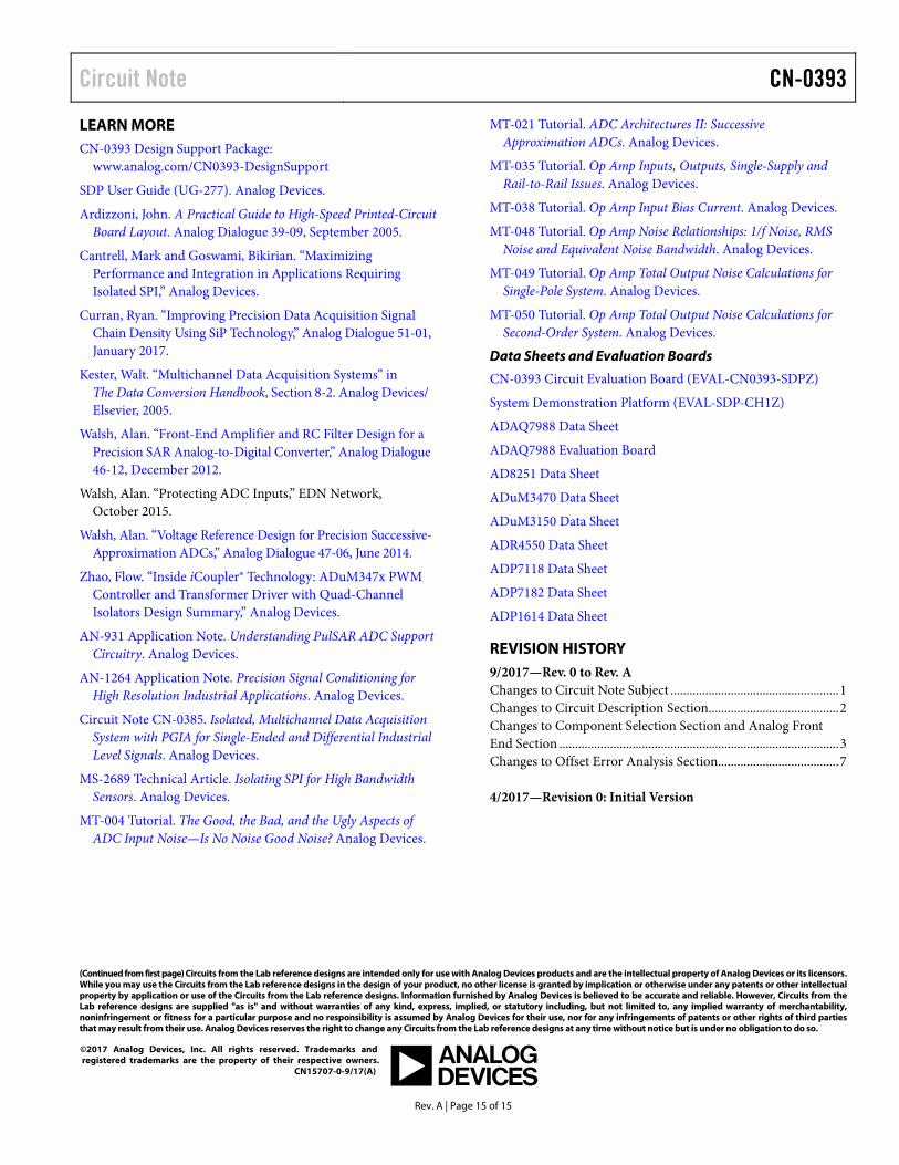
Figure 11 shows a photograph of the EVAL-CN0393-FMCZ board.
EVAL-CN0393-FMCZ
160-
PIN
FM
C
EVAL-SDP-CH1Z
12V
+12V_VIN
USB PC
1570
7-00
7
Figure 10. CN-0393 Evaluation Hardware Connections
1570
7-00
8
Figure 11. Photograph of EVAL-CN0393-FMCZ Board
Circuit Note CN-0393
Rev. A | Page 15 of 15
LEARN MORE CN-0393 Design Support Package:
www.analog.com/CN0393-DesignSupport
SDP User Guide (UG-277). Analog Devices.
Ardizzoni, John. A Practical Guide to High-Speed Printed-Circuit Board Layout. Analog Dialogue 39-09, September 2005.
Cantrell, Mark and Goswami, Bikirian. “Maximizing Performance and Integration in Applications Requiring Isolated SPI,” Analog Devices.
Curran, Ryan. “Improving Precision Data Acquisition Signal Chain Density Using SiP Technology,” Analog Dialogue 51-01, January 2017.
Kester, Walt. “Multichannel Data Acquisition Systems” in The Data Conversion Handbook, Section 8-2. Analog Devices/ Elsevier, 2005.
Walsh, Alan. “Front-End Amplifier and RC Filter Design for a Precision SAR Analog-to-Digital Converter,” Analog Dialogue 46-12, December 2012.
Walsh, Alan. “Protecting ADC Inputs,” EDN Network, October 2015.
Walsh, Alan. “Voltage Reference Design for Precision Successive-Approximation ADCs,” Analog Dialogue 47-06, June 2014.
Zhao, Flow. “Inside iCoupler® Technology: ADuM347x PWM Controller and Transformer Driver with Quad-Channel Isolators Design Summary,” Analog Devices.
AN-931 Application Note. Understanding PulSAR ADC Support Circuitry. Analog Devices.
AN-1264 Application Note. Precision Signal Conditioning for High Resolution Industrial Applications. Analog Devices.
Circuit Note CN-0385. Isolated, Multichannel Data Acquisition System with PGIA for Single-Ended and Differential Industrial Level Signals. Analog Devices.
MS-2689 Technical Article. Isolating SPI for High Bandwidth Sensors. Analog Devices.
MT-004 Tutorial. The Good, the Bad, and the Ugly Aspects of ADC Input Noise—Is No Noise Good Noise? Analog Devices.
MT-021 Tutorial. ADC Architectures II: Successive Approximation ADCs. Analog Devices.
MT-035 Tutorial. Op Amp Inputs, Outputs, Single-Supply and Rail-to-Rail Issues. Analog Devices.
MT-038 Tutorial. Op Amp Input Bias Current. Analog Devices.
MT-048 Tutorial. Op Amp Noise Relationships: 1/f Noise, RMS Noise and Equivalent Noise Bandwidth. Analog Devices.
MT-049 Tutorial. Op Amp Total Output Noise Calculations for Single-Pole System. Analog Devices.
MT-050 Tutorial. Op Amp Total Output Noise Calculations for Second-Order System. Analog Devices.
Data Sheets and Evaluation Boards
CN-0393 Circuit Evaluation Board (EVAL-CN0393-SDPZ)
System Demonstration Platform (EVAL-SDP-CH1Z)
ADAQ7988 Data Sheet
ADAQ7988 Evaluation Board
AD8251 Data Sheet
ADuM3470 Data Sheet
ADuM3150 Data Sheet
ADR4550 Data Sheet
ADP7118 Data Sheet
ADP7182 Data Sheet
ADP1614 Data Sheet
REVISION HISTORY 9/2017—Rev. 0 to Rev. A Changes to Circuit Note Subject ..................................................... 1 Changes to Circuit Description Section......................................... 2 Changes to Component Selection Section and Analog Front End Section ........................................................................................ 3 Changes to Offset Error Analysis Section...................................... 7 4/2017—Revision 0: Initial Version
(Continued from first page) Circuits from the Lab reference designs are intended only for use with Analog Devices products and are the intellectual property of Analog Devices or its licensors. While you may use the Circuits from the Lab reference designs in the design of your product, no other license is granted by implication or otherwise under any patents or other intellectual property by application or use of the Circuits from the Lab reference designs. Information furnished by Analog Devices is believed to be accurate and reliable. However, Circuits from the Lab reference designs are supplied "as is" and without warranties of any kind, express, implied, or statutory including, but not limited to, any implied warranty of merchantability, noninfringement or fitness for a particular purpose and no responsibility is assumed by Analog Devices for their use, nor for any infringements of patents or other rights of third parties that may result from their use. Analog Devices reserves the right to change any Circuits from the Lab reference designs at any time without notice but is under no obligation to do so.
©2017 Analog Devices, Inc. All rights reserved. Trademarks and registered trademarks are the property of their respective owners. CN15707-0-9/17(A)
![Fullerene Derivatives (CN-[OH]β) and Carbon Nanotubes ...](https://static.fdocument.org/doc/165x107/627f787abc5d8f553f2a99ec/fullerene-derivatives-cn-oh-and-carbon-nanotubes-.jpg)