CMOS Voltage and Current Reference Circuits consisting of...
26
1 CMOS Voltage and Current Reference Circuits consisting of Subthreshold MOSFETs — Micropower Circuit Components for Power-aware LSI Applications — Ken Ueno Hokkaido University Japan 1. Introduction The development of ultra-low power LSIs is a promising area of research in microelectronics. Such LSIs would be suitable for use in power-aware LSI applications such as portable mobile devices, implantable medical devices, and smart sensor networks [1]. These devices have to operate with ultra-low power, i.e., a few microwatts or less, because they will probably be placed under conditions where they have to get the necessary energy from poor energy sources such as microbatteries or energy scavenging devices [2]. As a step toward such LSIs, we first need to develop voltage and current reference circuits that can operate with an ultra-low current, several tens of nanoamperes or less, i.e., sub-microwatt operation. To achieve such low-power operation, the circuits have to be operated in the subthreshold region, i.e., a region at which the gate-source voltage of MOSFETs is lower than the threshold voltage [3; 4]. Voltage and current reference circuits are important building blocks for analog, digital, and mixed-signal circuit systems in microelectronics, because the performance of these circuits is determined mainly by their bias voltages and currents. The circuits generate a constant reference voltage and current for various other components such as operational amplifiers, comparators, AD/DA converters, oscillators, and PLLs. For this purpose, bandgap reference circuits with CMOS-based vertical bipolar transistors are conventionally used in CMOS LSIs [5; 6]. However, they need resistors with a high resistance of several hundred megaohms to achieve low-current, subthreshold operation. Such a high resistance needs a large area to be implemented, and this makes conventional bandgap references unsuitable for use in ultra-low power LSIs. Therefore, modified voltage and current reference circuits for lowpower LSIs have been reported (see [7]-[12], [14]-[17]). However, these circuits have various problems. For example, their power dissipations are still large, their output voltages and currents are sensitive to supply voltage and temperature variations, and they have complex circuits with many MOSFETs; these problems are inconvenient for practical use in ultra-low power LSIs. Moreover, the effect of process variations on the reference signal has not been discussed in detail. To solve these problems, I and my colleagues reported new voltage and current reference circuits [13; 18] that can operate with sub-microwatt power dissipation and with low sensitivity to temperature and supply voltage. Our circuits consist of subthreshold MOSFET circuits and use no resistors. Source: Solid State Circuits Technologies, Book edited by: Jacobus W. Swart, ISBN 978-953-307-045-2, pp. 462, January 2010, INTECH, Croatia, downloaded from SCIYO.COM www.intechopen.com
Transcript of CMOS Voltage and Current Reference Circuits consisting of...
1
CMOS Voltage and Current Reference Circuits consisting of Subthreshold MOSFETs
— Micropower Circuit Components for Power-aware LSI Applications —
Ken Ueno Hokkaido University
Japan
1. Introduction
The development of ultra-low power LSIs is a promising area of research in
microelectronics. Such LSIs would be suitable for use in power-aware LSI applications such
as portable mobile devices, implantable medical devices, and smart sensor networks [1].
These devices have to operate with ultra-low power, i.e., a few microwatts or less, because
they will probably be placed under conditions where they have to get the necessary energy
from poor energy sources such as microbatteries or energy scavenging devices [2]. As a step
toward such LSIs, we first need to develop voltage and current reference circuits that can
operate with an ultra-low current, several tens of nanoamperes or less, i.e., sub-microwatt
operation. To achieve such low-power operation, the circuits have to be operated in the
subthreshold region, i.e., a region at which the gate-source voltage of MOSFETs is lower
than the threshold voltage [3; 4]. Voltage and current reference circuits are important
building blocks for analog, digital, and mixed-signal circuit systems in microelectronics,
because the performance of these circuits is determined mainly by their bias voltages and
currents. The circuits generate a constant reference voltage and current for various other
components such as operational amplifiers, comparators, AD/DA converters, oscillators,
and PLLs. For this purpose, bandgap reference circuits with CMOS-based vertical bipolar
transistors are conventionally used in CMOS LSIs [5; 6]. However, they need resistors with a
high resistance of several hundred megaohms to achieve low-current, subthreshold
operation. Such a high resistance needs a large area to be implemented, and this makes
conventional bandgap references unsuitable for use in ultra-low power LSIs. Therefore,
modified voltage and current reference circuits for lowpower LSIs have been reported (see
[7]-[12], [14]-[17]). However, these circuits have various problems. For example, their power
dissipations are still large, their output voltages and currents are sensitive to supply voltage
and temperature variations, and they have complex circuits with many MOSFETs; these
problems are inconvenient for practical use in ultra-low power LSIs. Moreover, the effect of
process variations on the reference signal has not been discussed in detail. To solve these
problems, I and my colleagues reported new voltage and current reference circuits [13; 18]
that can operate with sub-microwatt power dissipation and with low sensitivity to
temperature and supply voltage. Our circuits consist of subthreshold MOSFET circuits and
use no resistors. Source: Solid State Circuits Technologies, Book edited by: Jacobus W. Swart,
ISBN 978-953-307-045-2, pp. 462, January 2010, INTECH, Croatia, downloaded from SCIYO.COM
www.intechopen.com
Solid State Circuits Technologies
2
The following sections provide overviews of previous reported low-power reference circuits and a detailed explanation of our circuits. Section 2 describes the subthreshold current of MOSFETs and shows the temperature and process sensitivity of the current with a SPICE simulation. Section 3 describes the principle of conventional voltage and current reference circuits based on bandgap reference circuits. Sections 4 and 5 explain the operation principle of the reported voltage and current reference circuits and show the characteristics of prototype devices we made using 0.35-μm standard CMOS process technology. Finally, concluding remarks are presented in Sect. 6.
2. Subthreshold region (or weak inversion region) of MOSFETs
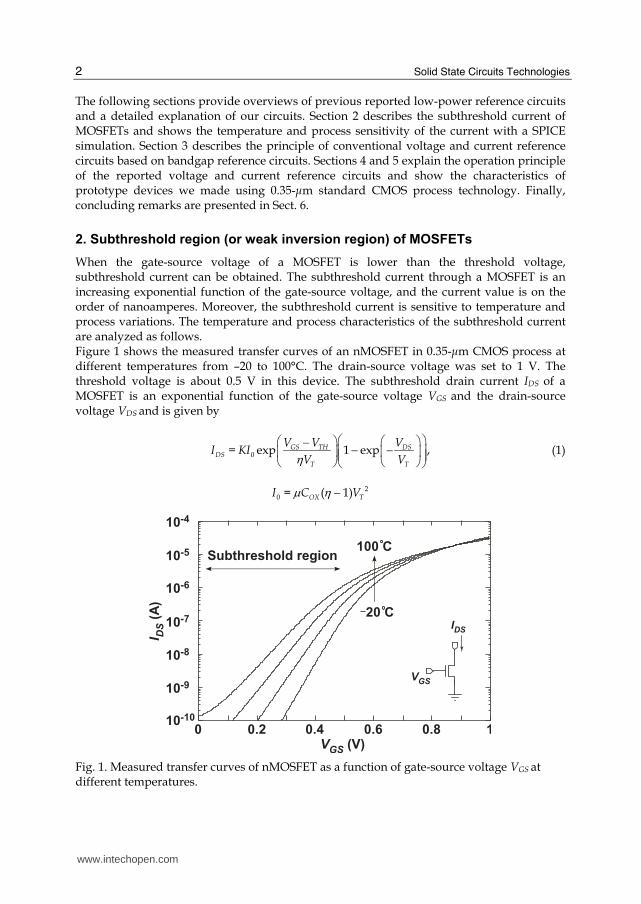
When the gate-source voltage of a MOSFET is lower than the threshold voltage, subthreshold current can be obtained. The subthreshold current through a MOSFET is an increasing exponential function of the gate-source voltage, and the current value is on the order of nanoamperes. Moreover, the subthreshold current is sensitive to temperature and process variations. The temperature and process characteristics of the subthreshold current are analyzed as follows. Figure 1 shows the measured transfer curves of an nMOSFET in 0.35-μm CMOS process at different temperatures from –20 to 100°C. The drain-source voltage was set to 1 V. The threshold voltage is about 0.5 V in this device. The subthreshold drain current IDS of a MOSFET is an exponential function of the gate-source voltage VGS and the drain-source voltage VDS and is given by
0= exp 1 exp ,GS TH DSDS
T T
V V VI KI
V Vη⎛ ⎞⎛ ⎞ ⎛ ⎞− − −⎜ ⎟⎜ ⎟ ⎜ ⎟⎜ ⎟⎝ ⎠ ⎝ ⎠⎝ ⎠ (1)
20 = ( 1)OX TI C Vμ η −
0 0.2 0.4 0.6 0.8 110-10
10-8
10-6
10-4
VGS
(V)
I DS (
A)
20 C
100 CSubthreshold region
VGS
IDS
10-9
10-7
10-5
Fig. 1. Measured transfer curves of nMOSFET as a function of gate-source voltage VGS at different temperatures.
www.intechopen.com
CMOS Voltage and Current Reference Circuits consisting of Subthreshold MOSFETs
3
where K is the aspect ratio (=W/L) of the transistor, μ is the carrier mobility, COX is the gate-oxide capacitance, VT(=kBT/q) is the thermal voltage, kB is the Boltzmann constant, T is the absolute temperature, and q is the elementary charge, VTH is the threshold voltage of a MOSFET, and η is the subthreshold slope factor [3], [19]. For VDS > 0.1 V, current IDS is independent of VDS and is given by
0= exp .GS THDS
T
V VI KI
Vη⎛ ⎞−⎜ ⎟⎝ ⎠ (2)
The temperature dependence of the threshold voltage VTH and the mobility μ of MOSFET can be given by
0= ,TH THV V Tκ− (3)
0 0( ) = ( )( / ) mT T T Tμ μ − (4)
where μ(T0) is the carrier mobility at room temperature T0, m is the mobility temperature
exponent, VTH0 is the threshold voltage at 0 K, and κ is the temperature coefficient of VTH
[20].
The temperature coefficient (T.C.) of the subthreshold current with fixed gate-source voltage
is given by
1
. . = DS
DS
dIT C
I dT
2
2
1 1 1= exp(( ) / )
exp(( ) / )T
GS TH T
T GS TH T
d dV dV V V
dT V dT V V V dT
μ ημ η+ + −−
2 ( ) /
= .GS TH
T
m V V T
T V
κη
− − −+ (5)
Process variations can be classified into two categories: i.e., within-die (WID) (intra-die)
variation and die-to-die (D2D) (inter-die) variation [21]-[23]. The WID variation is caused by
mismatches between transistor parameters within a chip and affects the relative accuracy of
the parameters. In contrast, the D2D variation affects the absolute accuracy of transistor
parameters between chips.
The process dependence of the subthreshold current can be expressed by
1
= = .DS DS DS THTH
DS DS TH T
I I I VV
I I V V
μμμ μ η⎛ ⎞Δ ∂ ∂ Δ ΔΔ + Δ −⎜ ⎟∂ ∂⎝ ⎠ (6)
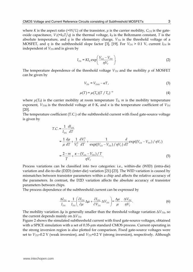
The mobility variation Δμ is generally smaller than the threshold voltage variation ΔVTH, so the current depends mainly on ΔVTH. Figure 2 shows the simulated subthreshold current with fixed gate-source voltages, obtained
with a SPICE simulation with a set of 0.35-μm standard CMOS process. Current operating in
the strong inversion region is also plotted for comparison. Fixed gate-source voltages were
set to VTH–0.2 V (weak inversion), and VTH+0.2 V (strong inversion), respectively. Although
www.intechopen.com
Solid State Circuits Technologies
4
IDS : Weak inversion (V
Bias=V
TH 0.2)
IDS : Strong inversion (V
Bias=V
TH + 0.2)
3%/ C
T.C.
0.5%/ C
2.5%/mV
ΔIDS
ΔVTH
0.8%/mV
1
10
100
0.1
0.010 0.05 0.10.050.1
ΔVTH
(V)
20 40 60 80200
Temperature ( C)
Cu
rren
t (I
DS
/ I
DS
(2
7 C
))
1
10
100
0.1
0.01
Cu
rren
t (I
DS
/ I
DS
(Typ
.))
IDS
: Weak inversion
IDS
: Strong inversion
VBias
IDS
VBias
IDS
(Subthreshold region)IDS
: Weak inversion
IDS
: Strong inversion
(Subthreshold region)
Fig. 2. (A). Simulated drain currents as a function of temperature. Fixed gate biases were set to VTH–0.2 V (weak inversion), and VTH+0.2 V (strong inversion). (B). Drain currents as a function of D2D threshold voltage variation ΔVTH, as obtained from Monte Carlo simulation of 300 runs.
the current in the strong inversion region has a small temperature dependence (0.5%/°C),
the subthreshold current has a large temperature dependence (3%/°C), as shown in Fig. 2-
(A). Figure 2-(B) shows the simulated subthreshold current as a function of the threshold
voltage variation ΔVTH, as obtained from Monte Carlo simulation of 300 runs, assuming
both die-to-die (D2D) variation (e.g., ΔVTH, Δμ, ΔTOX, ΔL, ΔW) and within die (WID)
variation (e.g., σVTH, σμ, σTOX, σL, σW) in transistor parameters [21; 22; 23]. Each open circle and
square show IDS for a run. The subthreshold current depends strongly on the threshold
voltage variation (2.5%/mV) in comparison with the strong inversion current (0.8%/mV).
Therefore, the subthreshold current is strongly dependent on temperature and process
variations. In circuit designs, the process sensitivity of the subthreshold current has to be
reduced by using large-sized transistors [23] and various analog layout techniques [24]. On
the other hand, the exponential behavior and the high sensitivity to temperature of the
subthreshold current can be used to compensate for temperature variation of a constant
voltage, such as voltage reference circuits.
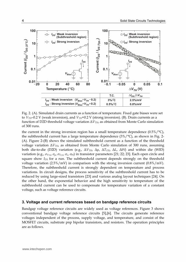
3. Voltage and current references based on bandgap reference circuits
Bandgap voltage reference circuits are widely used as voltage references. Figure 3 shows
conventional bandgap voltage reference circuits [5],[6]. The circuits generate reference
voltages independent of the process, supply voltage, and temperature, and consist of the
MOSFET circuits, substrate pnp bipolar transistors, and resistors. The operation principles
are as follows.
www.intechopen.com
CMOS Voltage and Current Reference Circuits consisting of Subthreshold MOSFETs
5
M1 M2
R4
VREF
IREF
Q2Q1
M1 M2
VREF
IP
Q2Q1 Q3
IREFIREFIPIP
(A) (B)
I1 I1I2I2
R2 R3
R1
I1 + I2=( )I1 + I2=( ) I1 + I2=( )
R2R1
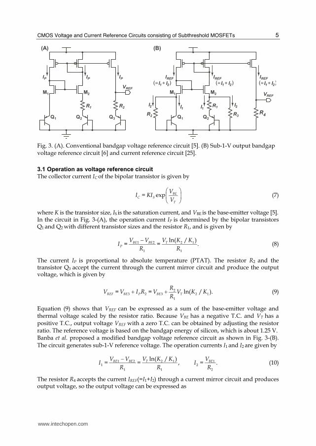
Fig. 3. (A). Conventional bandgap voltage reference circuit [5]. (B) Sub-1-V output bandgap voltage reference circuit [6] and current reference circuit [25].
3.1 Operation as voltage reference circuit
The collector current IC of the bipolar transistor is given by
= exp BEC S
T
VI KI
V
⎛ ⎞⎜ ⎟⎝ ⎠ (7)
where K is the transistor size, IS is the saturation current, and VBE is the base-emitter voltage [5]. In the circuit in Fig. 3-(A), the operation current IP is determined by the bipolar transistors Q1 and Q2 with different transistor sizes and the resistor R1, and is given by
1 2 2 1
1 1
ln( / )= = .BE BE T
P
V V V K KI
R R
− (8)
The current IP is proportional to absolute temperature (PTAT). The resistor R2 and the transistor Q3 accept the current through the current mirror circuit and produce the output voltage, which is given by
23 2 3 2 1
1
= = ln( / ).REF BE P BE T
RV V I R V V K K
R+ + (9)
Equation (9) shows that VREF can be expressed as a sum of the base-emitter voltage and thermal voltage scaled by the resistor ratio. Because VBE has a negative T.C. and VT has a positive T.C., output voltage VREF with a zero T.C. can be obtained by adjusting the resistor ratio. The reference voltage is based on the bandgap energy of silicon, which is about 1.25 V. Banba et al. proposed a modified bandgap voltage reference circuit as shown in Fig. 3-(B). The circuit generates sub-1-V reference voltage. The operation currents I1 and I2 are given by
1 2 2 1 11 2
1 1 2
ln( / )= = , = .BE BE T BEV V V K K V
I IR R R
− (10)
The resistor R4 accepts the current IREF(=I1+I2) through a current mirror circuit and produces output voltage, so the output voltage can be expressed as
www.intechopen.com
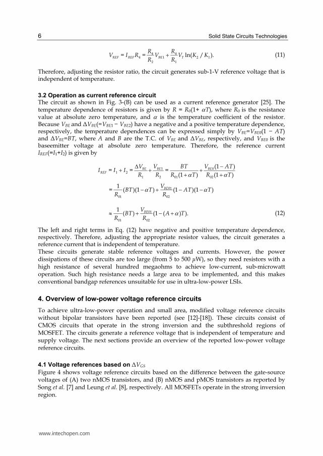
Solid State Circuits Technologies
6
4 44 1 2 1
2 1
= = ln( / ).REF REF BE T
R RV I R V V K K
R R+ (11)
Therefore, adjusting the resistor ratio, the circuit generates sub-1-V reference voltage that is independent of temperature.
3.2 Operation as current reference circuit The circuit as shown in Fig. 3-(B) can be used as a current reference generator [25]. The temperature dependence of resistors is given by R = R0(1+ αT), where R0 is the resistance value at absolute zero temperature, and α is the temperature coefficient of the resistor. Because VBE and ΔVBE(=VBE1 − VBE2) have a negative and a positive temperature dependence, respectively, the temperature dependences can be expressed simply by VBE=VBE0(1 − AT) and ΔVBE=BT, where A and B are the T.C. of VBE and ΔVBE, respectively, and VBE0 is the baseemitter voltage at absolute zero temperature. Therefore, the reference current IREF(=I1+I2) is given by
1 01 2
1 2 01 02
(1 )= = =
(1 ) (1 )BE BE BE
REF
V V BT V ATI I I
R R R T R Tα αΔ −+ + ++ +
01
01 02
1= ( )(1 ) (1 )(1 )BEV
BT T AT TR R
α α− + − −
01
01 02
1( ) (1 ( ) ).BEVBT A T
R Rα≈ + − + (12)
The left and right terms in Eq. (12) have negative and positive temperature dependence, respectively. Therefore, adjusting the appropriate resistor values, the circuit generates a reference current that is independent of temperature. These circuits generate stable reference voltages and currents. However, the power dissipations of these circuits are too large (from 5 to 500 μW), so they need resistors with a high resistance of several hundred megaohms to achieve low-current, sub-microwatt operation. Such high resistance needs a large area to be implemented, and this makes conventional bandgap references unsuitable for use in ultra-low-power LSIs.
4. Overview of low-power voltage reference circuits
To achieve ultra-low-power operation and small area, modified voltage reference circuits without bipolar transistors have been reported (see [12]-[18]). These circuits consist of CMOS circuits that operate in the strong inversion and the subthreshold regions of MOSFET. The circuits generate a reference voltage that is independent of temperature and supply voltage. The next sections provide an overview of the reported low-power voltage reference circuits.
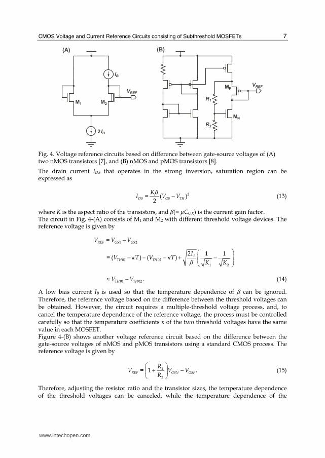
4.1 Voltage references based on ΔVGS
Figure 4 shows voltage reference circuits based on the difference between the gate-source voltages of (A) two nMOS transistors, and (B) nMOS and pMOS transistors as reported by Song et al. [7] and Leung et al. [8], respectively. All MOSFETs operate in the strong inversion region.
www.intechopen.com
CMOS Voltage and Current Reference Circuits consisting of Subthreshold MOSFETs
7
(A)
MN
VREF
(B)
VREF
IB
IB2
M1 M2
MP
R1
R2
Fig. 4. Voltage reference circuits based on difference between gate-source voltages of (A) two nMOS transistors [7], and (B) nMOS and pMOS transistors [8].
The drain current IDS that operates in the strong inversion, saturation region can be expressed as
2= ( )2
DS GS TH
KI V V
β − (13)
where K is the aspect ratio of the transistors, and β(= μCOX) is the current gain factor. The circuit in Fig. 4-(A) consists of M1 and M2 with different threshold voltage devices. The reference voltage is given by
1 2=REF GS GSV V V−
01 02
1 2
2 1 1= ( ) ( ) B
TH TH
IV T V T
K Kκ κ β
⎛ ⎞− − − + −⎜ ⎟⎜ ⎟⎝ ⎠
01 02 .TH THV V≈ − (14)
A low bias current IB is used so that the temperature dependence of β can be ignored. Therefore, the reference voltage based on the difference between the threshold voltages can be obtained. However, the circuit requires a multiple-threshold voltage process, and, to cancel the temperature dependence of the reference voltage, the process must be controlled carefully so that the temperature coefficients κ of the two threshold voltages have the same value in each MOSFET. Figure 4-(B) shows another voltage reference circuit based on the difference between the gate-source voltages of nMOS and pMOS transistors using a standard CMOS process. The reference voltage is given by
1
2
= 1 .REF GSN GSP
RV V V
R
⎛ ⎞+ −⎜ ⎟⎝ ⎠ (15)
Therefore, adjusting the resistor ratio and the transistor sizes, the temperature dependence of the threshold voltages can be canceled, while the temperature dependence of the
www.intechopen.com
Solid State Circuits Technologies
8
mobilities can be canceled only at room temperature. Consequently, the T.C. of the output voltage will be degraded for a wide temperature range. As reported in [8], a measured T.C. of 36.9 ppm/°C and a power dissipation of 30 μW were obtained. However, the power dissipation is still too large for use with sub-microwatt operation. To reduce the power dissipation, the circuit requires resistors with high resistance.
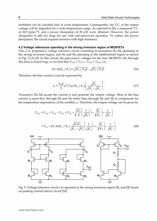
4.2 Voltage references operating in the strong inversion region of MOSFETs
Vita et al. proposed a voltage reference circuit consisting of transistors M3–M8 operating in the strong inversion region, and M1 and M2 operating in the subthreshold region as shown in Fig. 5-(A) [9]. In this circuit, the gate-source voltages for the four MOSFETs (M1 through M4) form a closed loop, so we find that VGS3 + VGS1 = VGS2 + VGS4, i.e.,
2 1 4 3ln( / ) = 2 / 2 / .T B BV K K I K I Kη β β− (16)
Therefore, the bias current IB can be expressed by
2
32 2 242 1
3 4
= ( / ) .ln2
B T
KKI V K K
K K
β η ⎛ ⎞⎜ ⎟⎜ ⎟−⎝ ⎠ (17)
Transistors M5–M8 accept the current IB and generate the output voltage. Most of the bias
current IB must flow through M7 and M8 rather than through M5 and M6 to compensate for
the temperature dependence of the mobility μ. Therefore, the output voltage can be given by
68 5 7
58 7
2 1 1= = 1B
REF GS GS GS TH
I KV V V V V
KK Kβ⎛ ⎞⎛ ⎞+ − + + −⎜ ⎟⎜ ⎟⎜ ⎟⎜ ⎟⎝ ⎠⎝ ⎠
3 4 62 1
53 4 8 7
1 1= ln( / ) 1 .TH T
K K KV V K K
KK K K Kη ⎛ ⎞⎛ ⎞+ + −⎜ ⎟⎜ ⎟⎜ ⎟⎜ ⎟− ⎝ ⎠⎝ ⎠ (18)
VREF
M1 M2
R1
R2VREF
M1 M2
M3 M4
M5
M6
M7
M8
(B)(A)
IB IB IB
IB IB
Fig. 5. Voltage reference circuit (A) operated in the strong inversion region [9], and (B) based on peaking current mirror circuit [10].
www.intechopen.com
CMOS Voltage and Current Reference Circuits consisting of Subthreshold MOSFETs
9
Because VTH in Eq. (3) has a negative T.C. and VT has a positive T.C., output voltage VREF
with a zero T.C. can be obtained by adjusting the size of the transistors. As reported in [9], a measured T.C. of 12 ppm/°C and a power dissipation of 0.12 μW were
obtained. Although the operation current of the circuit is on the order of nanoamperes,
transistors M3–M8 operate in the strong inversion, saturation region. So, designs with careful
transistor sizing are required for operation in each of the regions in MOSFETs.
4.3 Voltage references operating in the subthreshold region of MOSFETs
Cheng et al. developed a voltage reference using a peaking current mirror circuit as shown
in Fig. 5-(B) [10]. All MOSFETs operate in the subthreshold region. The circuit forms a
closed loop, i.e., VGS1 = VGS2 − IBR2, so the bias currents IB can be expressed by
2 1 1 2
2 2
ln( / )= = .GS GS T
B
V V V K KI
R R
η− (19)
The output voltage is given by
2 1=REF GS BV V I R+
12 1 2
2
= ln( / ).GS T
RV V K K
Rη+ (20)
Because VGS and VT have a negative and a positive T.C., respectively, output voltage VREF
with a zero T.C. can be obtained by adjusting the resistor ratio. As reported in [10], a
measured temperature coefficient of 62 ppm/°C and a power dissipation of 4.6 μW were
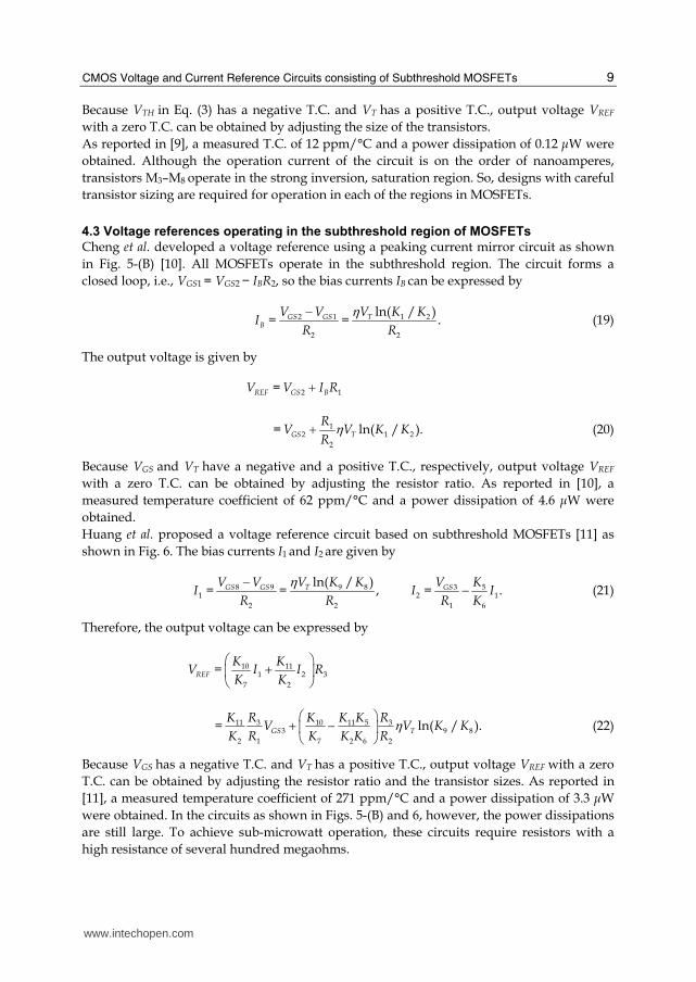
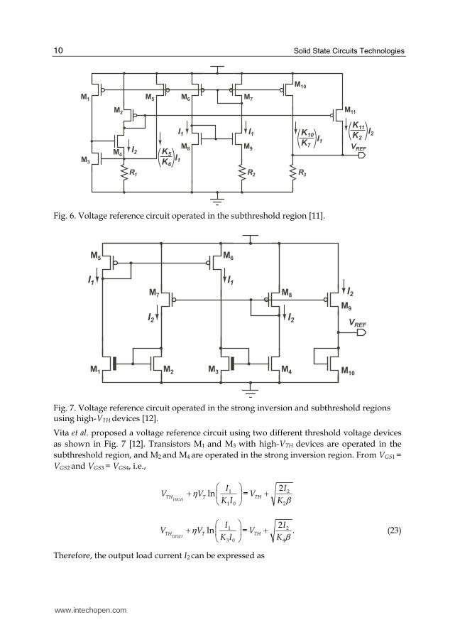
obtained. Huang et al. proposed a voltage reference circuit based on subthreshold MOSFETs [11] as
shown in Fig. 6. The bias currents I1 and I2 are given by
8 9 9 8 3 51 2 1
2 2 1 6
ln( / )= = , = .GS GS T GSV V V K K V K
I I IR R R K
η− − (21)
Therefore, the output voltage can be expressed by
10 111 2 3
7 2
=REF
K KV I I R
K K
⎛ ⎞+⎜ ⎟⎝ ⎠
11 3 10 11 5 33 9 8
2 1 7 2 6 2
= ln( / ).GS T
K R K K K RV V K K
K R K K K Rη⎛ ⎞+ −⎜ ⎟⎝ ⎠ (22)
Because VGS has a negative T.C. and VT has a positive T.C., output voltage VREF with a zero
T.C. can be obtained by adjusting the resistor ratio and the transistor sizes. As reported in
[11], a measured temperature coefficient of 271 ppm/°C and a power dissipation of 3.3 μW
were obtained. In the circuits as shown in Figs. 5-(B) and 6, however, the power dissipations
are still large. To achieve sub-microwatt operation, these circuits require resistors with a
high resistance of several hundred megaohms.
www.intechopen.com
Solid State Circuits Technologies
10
M3
VREF
M2
M1 M5 M6 M7
M8 M9
M10
M11
M4
I1 I1
I1
I2
R1 R2 R3
K6
K5
I1K7
K10I2K2
K11
Fig. 6. Voltage reference circuit operated in the subthreshold region [11].
VREF
M7 M8
M3 M4
M9
M5 M6
M1 M2 M10
I2
I2
I1 I1
I2
Fig. 7. Voltage reference circuit operated in the strong inversion and subthreshold regions using high-VTH devices [12].
Vita et al. proposed a voltage reference circuit using two different threshold voltage devices
as shown in Fig. 7 [12]. Transistors M1 and M3 with high-VTH devices are operated in the
subthreshold region, and M2 and M4 are operated in the strong inversion region. From VGS1 =
VGS2 and VGS3 = VGS4, i.e.,
1 2
1 0 2
2ln =
HIGHTH T TH
I IV V V
K I Kη β
⎛ ⎞+ +⎜ ⎟⎝ ⎠
1 2
3 0 4
2ln = .
HIGHTH T TH
I IV V V
K I Kη β
⎛ ⎞+ +⎜ ⎟⎝ ⎠ (23)
Therefore, the output load current I2 can be expressed as
www.intechopen.com
CMOS Voltage and Current Reference Circuits consisting of Subthreshold MOSFETs
11
2 2 242 3 12
4 2
= ( / ).ln2( / 1)
T
KI V K K
K K
β η− (24)
Transistor M10 accepts the current I2, and the output voltage can be given by
2
10
2=REF TH
IV V
K β+
4 103 1
4 2
/= ln( / ) .
/ 1TH T
K KV V K K
K Kη+ − (25)
Because VTH has a negative T.C. and VT has a positive T.C., output voltage VREF with a zero T.C. can be obtained by adjusting the size of the transistors. As reported in [12], a measured T.C. of 10 ppm/°C and a power dissipation of 0.036 μW were obtained. However, the circuit requires a high-VTH devices.
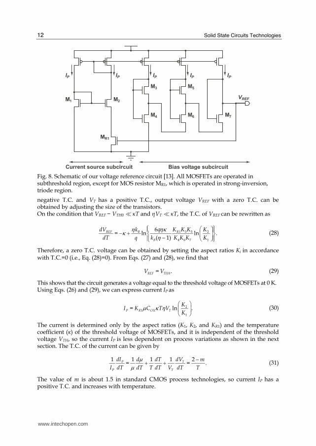
4.4 Voltage references consisting of subthreshold MOSFETs Figure 8 shows our voltage reference circuit, which consists of a current source subcircuit and a bias-voltage subcircuit [13]. The current source subcircuit is a modified β multiplier self-biasing circuit that uses a MOS resistor MR1 instead of ordinary resistors. All the MOSFETs except for MR1 operate in the subthreshold region. MOS resistor MR1 is operated in a strong-inversion, deep-triode region. The circuit generates two voltages, one with a negative T.C. and one with a positive T.C., and combines them to produce a constant voltage with a zero T.C.. In the current source subcircuit, the current IP is determined by two transistors M1 and M2, and the MOS resistor MR1. The current IP is given by
1
1
= DSRP
RM
VI
R
1 2 1= ( ) ln( / ).R OX REF TH TK C V V V K Kμ η− (26)
In the bias-voltage subcircuit, the gate-source voltages (VGS3 through VGS7) of the transistors form a closed loop [26], and the currents in M4 and M6 are 3IP and 2IP. Therefore, we find that output voltage VREF of the circuit is given by
4 3 6 5 7=REF GS GS GS GS GSV V V V V V− + − +
3 54
6 7
2= lnGS T
K KV V
K Kη ⎛ ⎞+ ⎜ ⎟⎝ ⎠
3 5
4 0 6 7
3 2= ln lnP
TH T T
I K KV V V
K I K Kη η⎛ ⎞ ⎛ ⎞+ +⎜ ⎟ ⎜ ⎟⎝ ⎠ ⎝ ⎠ (27)
where we assume that the mismatch between the threshold voltages of the transistors can be ignored. Equation (27) shows that VREF can be expressed as a sum of the gate-source voltage VGS4 and thermal voltage VT scaled by the transistor sizes. Because VTH in Eq. (3) has a
www.intechopen.com
Solid State Circuits Technologies
12
VREFM1 M2
M3
M4
M5
M6 M7
MR1
IP IP IP IPIP
Current source subcircuit Bias voltage subcircuit
Fig. 8. Schematic of our voltage reference circuit [13]. All MOSFETs are operated in subthreshold region, except for MOS resistor MR1, which is operated in strong-inversion, triode region.
negative T.C. and VT has a positive T.C., output voltage VREF with a zero T.C. can be obtained by adjusting the size of the transistors. On the condition that VREF − VTH0 2 κT and ηVT 2 κT, the T.C. of VREF can be rewritten as
1 3 5 2
4 6 7 1
6= ln ln .
( 1)REF B R
B
qdV k K K K K
dT q k K K K K
ηκηκ η⎧ ⎫⎛ ⎞⎪ ⎪− + ⎨ ⎬⎜ ⎟−⎪ ⎪⎝ ⎠⎩ ⎭ (28)
Therefore, a zero T.C. voltage can be obtained by setting the aspect ratios Ki in accordance with T.C.=0 (i.e., Eq. (28)=0). From Eqs. (27) and (28), we find that
0= .REF THV V (29)
This shows that the circuit generates a voltage equal to the threshold voltage of MOSFETs at 0 K. Using Eqs. (26) and (29), we can express current IP as
21
1
= ln .P R OX T
KI K C T V
Kμ κ η ⎛ ⎞⎜ ⎟⎝ ⎠ (30)
The current is determined only by the aspect ratios (K1, K2, and KR1) and the temperature coefficient (κ) of the threshold voltage of MOSFETs, and it is independent of the threshold voltage VTH, so the current IP is less dependent on process variations as shown in the next section. The T.C. of the current can be given by
1 1 1 1 2
= = .P T
P T
dI d dT dV m
I dT dT T dT V dT T
μμ
−+ + (31)
The value of m is about 1.5 in standard CMOS process technologies, so current IP has a positive T.C. and increases with temperature.
www.intechopen.com
CMOS Voltage and Current Reference Circuits consisting of Subthreshold MOSFETs
13
0
10
20
30
40
Oc
cu
rre
nc
es 50
60
70
0.7
0.8
0.9
1.0
VR
EF (
V)
0 0.05 0.10.050.1
ΔVTH
(V)
0.6 0.7 0.8 0.9 1.0
VREF
(V)
(A) (B)
ΔVREF
/ΔVTH
~~ 1
1.1
µ = 0.84 V
σ = 0.06 V
σ/µ = 7 %
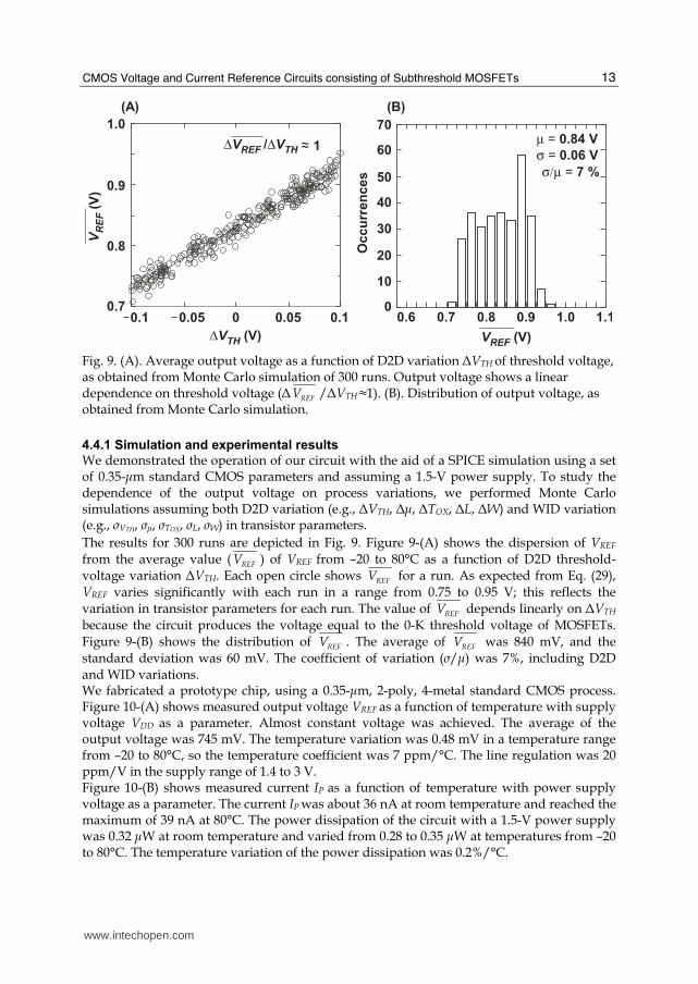
Fig. 9. (A). Average output voltage as a function of D2D variation ΔVTH of threshold voltage, as obtained from Monte Carlo simulation of 300 runs. Output voltage shows a linear dependence on threshold voltage (Δ REFV /ΔVTH ≈1). (B). Distribution of output voltage, as obtained from Monte Carlo simulation.
4.4.1 Simulation and experimental results
We demonstrated the operation of our circuit with the aid of a SPICE simulation using a set of 0.35-μm standard CMOS parameters and assuming a 1.5-V power supply. To study the dependence of the output voltage on process variations, we performed Monte Carlo simulations assuming both D2D variation (e.g., ΔVTH, Δμ, ΔTOX, ΔL, ΔW) and WID variation (e.g., σVTH, σμ, σTOX, σL, σW) in transistor parameters.
The results for 300 runs are depicted in Fig. 9. Figure 9-(A) shows the dispersion of VREF
from the average value ( REFV ) of VREF from –20 to 80°C as a function of D2D threshold-
voltage variation ΔVTH. Each open circle shows REFV for a run. As expected from Eq. (29),
VREF varies significantly with each run in a range from 0.75 to 0.95 V; this reflects the
variation in transistor parameters for each run. The value of REFV depends linearly on ΔVTH
because the circuit produces the voltage equal to the 0-K threshold voltage of MOSFETs.
Figure 9-(B) shows the distribution of REFV . The average of REFV was 840 mV, and the
standard deviation was 60 mV. The coefficient of variation (σ/μ) was 7%, including D2D
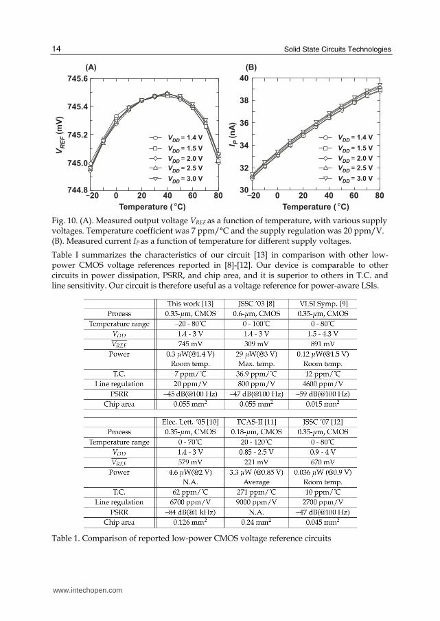
and WID variations. We fabricated a prototype chip, using a 0.35-μm, 2-poly, 4-metal standard CMOS process. Figure 10-(A) shows measured output voltage VREF as a function of temperature with supply voltage VDD as a parameter. Almost constant voltage was achieved. The average of the output voltage was 745 mV. The temperature variation was 0.48 mV in a temperature range from –20 to 80°C, so the temperature coefficient was 7 ppm/°C. The line regulation was 20 ppm/V in the supply range of 1.4 to 3 V. Figure 10-(B) shows measured current IP as a function of temperature with power supply voltage as a parameter. The current IP was about 36 nA at room temperature and reached the maximum of 39 nA at 80°C. The power dissipation of the circuit with a 1.5-V power supply was 0.32 μW at room temperature and varied from 0.28 to 0.35 μW at temperatures from –20 to 80°C. The temperature variation of the power dissipation was 0.2%/°C.
www.intechopen.com
Solid State Circuits Technologies
14
I P (
nA
)
30
32
34
36
38
40
20 40 60 80200
VDD
= 1.4 V
VDD
= 1.5 V
VDD
= 2.0 V
VDD
= 2.5 V
VDD
= 3.0 V
20 40 60 80200
VDD
= 1.4 V
VDD
= 1.5 V
VDD
= 2.0 V
VDD
= 2.5 V
VDD
= 3.0 V
744.8
745.0
745.2
745.4
745.6
VR
EF (
mV
)(A) (B)
Temperature ( C) Temperature ( C)
Fig. 10. (A). Measured output voltage VREF as a function of temperature, with various supply voltages. Temperature coefficient was 7 ppm/°C and the supply regulation was 20 ppm/V. (B). Measured current IP as a function of temperature for different supply voltages.
Table I summarizes the characteristics of our circuit [13] in comparison with other low-power CMOS voltage references reported in [8]-[12]. Our device is comparable to other circuits in power dissipation, PSRR, and chip area, and it is superior to others in T.C. and line sensitivity. Our circuit is therefore useful as a voltage reference for power-aware LSIs.
Table 1. Comparison of reported low-power CMOS voltage reference circuits
www.intechopen.com
CMOS Voltage and Current Reference Circuits consisting of Subthreshold MOSFETs
15
4.4.2 Discussion
Our circuit has several possible applications. The output voltage of our circuit can be used as a monitor signal for the D2D process variation in MOSFET threshold voltage because the output voltage is equal to the 0-K threshold voltage of MOSFETs in an LSI chip and is linearly dependent on the VTH variation, as shown in Fig. 9-(A). This output voltage can be used to compensate for the threshold voltage variation in LSI chips. For example, consider the application to a reference current source. The process variation of the current IP flowing in the circuit as shown in Fig. 8 (see Eq. (30)) can be expressed as
1=P P P P
OX
P P OX
I I I IC
I I Cμ κμ κ
⎛ ⎞Δ ∂ ∂ ∂Δ + Δ + Δ⎜ ⎟∂ ∂ ∂⎝ ⎠
= .OX
OX
C
C
μ κμ κΔ Δ Δ+ + (32)
The current is independent of the threshold voltage variation. Although the current depends on the variation of the mobility Δμ/μ, gate-oxide capacitance ΔCOX/COX, and the temperature coefficient of the threshold voltage Δκ/κ, these variations are far smaller than the threshold voltage variation. This way, the circuit can be used as an elementary circuit block for on-chip D2D process compensation systems, such as process- and temperature-compensated current references [27].
5. Overview of low-power current reference circuits
Current references with nanoampere-order currents are required to ensure circuit operation that is stable and highly precise, because power dissipation and performance of circuits are determined mainly by their bias currents. Nanoampere-current references for ultra-low-power LSIs have been reported in several papers [13]-[15]. The next sections provide an overview of the reported nanoampere current reference circuits.
5.1 Current references based on weak and strong inversion regions of MOSFETs
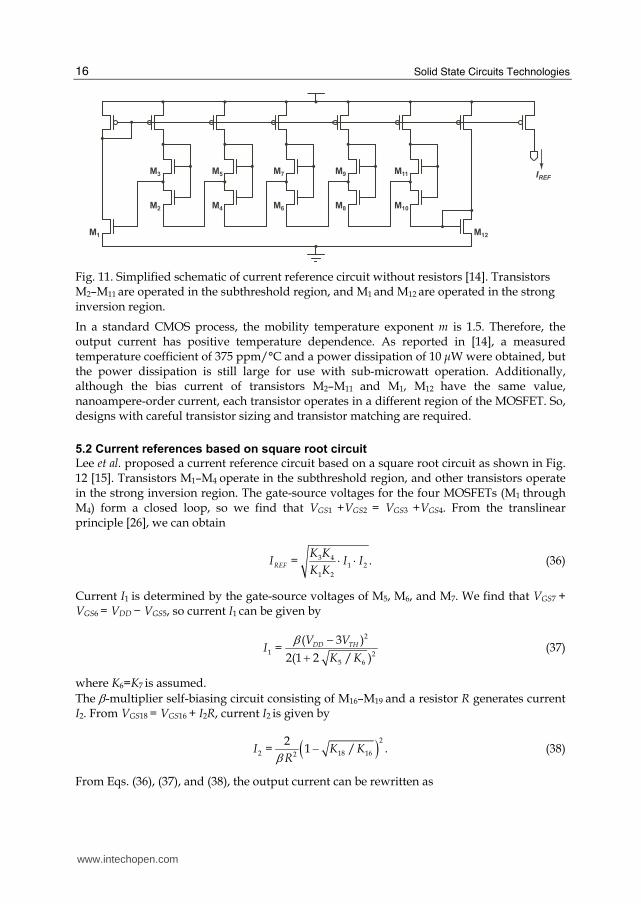
Sansen et al. developed a current reference circuit without resistors as shown in Fig. 11 [14]. Transistors M2–M11 operate in the subthreshold region, and M1 and M12 operate in the strong inversion region. The gate-source voltages of M1–M12 form a closed loop, so we find that
1 12 10 11 8 9 6 7 4 5 2 3= .GS GS GS GS GS GS GS GS GS GS GS GSV V V V V V V V V V V V+ − + − + − + − + − (33)
Assuming that the body effects of M2–M10 are ignored, the output current IREF is given by
2 2 2 11 9 7 5 3 1 12
10 8 6 4 2 12 1
= 120 .ln2
REF T
K K K K K K KI V
K K K K K K K
β η ⎛ ⎞⎛ ⎞⋅⎜ ⎟⎜ ⎟−⎝ ⎠⎝ ⎠ (34)
The T.C. of the reference current is given by
2
2
1 1 1 2. . = = = .REF T
REF T
dI d dV mT C
I dT dT V dT T
μμ
−+ (35)
www.intechopen.com
Solid State Circuits Technologies
16
M12M1
M2
IREFM3
M4
M5
M6
M7
M8
M9
M10
M11
Fig. 11. Simplified schematic of current reference circuit without resistors [14]. Transistors M2–M11 are operated in the subthreshold region, and M1 and M12 are operated in the strong inversion region.
In a standard CMOS process, the mobility temperature exponent m is 1.5. Therefore, the output current has positive temperature dependence. As reported in [14], a measured temperature coefficient of 375 ppm/°C and a power dissipation of 10 μW were obtained, but the power dissipation is still large for use with sub-microwatt operation. Additionally, although the bias current of transistors M2–M11 and M1, M12 have the same value, nanoampere-order current, each transistor operates in a different region of the MOSFET. So, designs with careful transistor sizing and transistor matching are required.
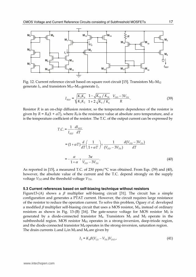
5.2 Current references based on square root circuit
Lee et al. proposed a current reference circuit based on a square root circuit as shown in Fig. 12 [15]. Transistors M1–M4 operate in the subthreshold region, and other transistors operate in the strong inversion region. The gate-source voltages for the four MOSFETs (M1 through M4) form a closed loop, so we find that VGS1 +VGS2 = VGS3 +VGS4. From the translinear principle [26], we can obtain
3 41 2
1 2
= .REF
K KI I I
K K⋅ ⋅ (36)
Current I1 is determined by the gate-source voltages of M5, M6, and M7. We find that VGS7 + VGS6 = VDD − VGS5, so current I1 can be given by
2
1 25 6
( 3 )=
2(1 2 / )DD THV V
IK K
β −+ (37)
where K6=K7 is assumed.
The β-multiplier self-biasing circuit consisting of M16–M19 and a resistor R generates current I2. From VGS18 = VGS16 + I2R, current I2 is given by
( )2
2 18 162
2= 1 / .I K K
Rβ − (38)
From Eqs. (36), (37), and (38), the output current can be rewritten as
www.intechopen.com
CMOS Voltage and Current Reference Circuits consisting of Subthreshold MOSFETs
17
M14
M1
M2
M4
M3M16 M
18
M17 M19
M15
M13M8M5
M6
M7
M12M10
M11M9
IREF
I2
I1
R
Fig. 12. Current reference circuit based on square root circuit [15]. Transistors M5–M12
generate I1, and transistors M13–M19 generate I2.
18 163 4
1 2 5 6
1 / 3= .
1 2 /DD TH
REF
K KK K V VI
K K RK K
− −⋅ ⋅+ (39)
Resistor R is an on-chip diffusion resistor, so the temperature dependence of the resistor is
given by R = R0(1 + αT), where R0 is the resistance value at absolute zero temperature, and α is the temperature coefficient of the resistor. The T.C. of the output current can be expressed by
1
. . = REF
REF
dIT C
I dT
1 1 ( 3 )
= (1 )1 ( 3 )
DD TH
DD TH
d d V VT
dT T V V dTα α
−⎛ ⎞+ +⎜ ⎟+ −⎝ ⎠
3
= .1 3DD THV V
α κα− ++ − (40)
As reported in [15], a measured T.C. of 230 ppm/°C was obtained. From Eqs. (39) and (40), however, the absolute value of the current and the T.C. depend strongly on the supply voltage VDD and the threshold voltage VTH.
5.3 Current references based on self-biasing technique without resistors
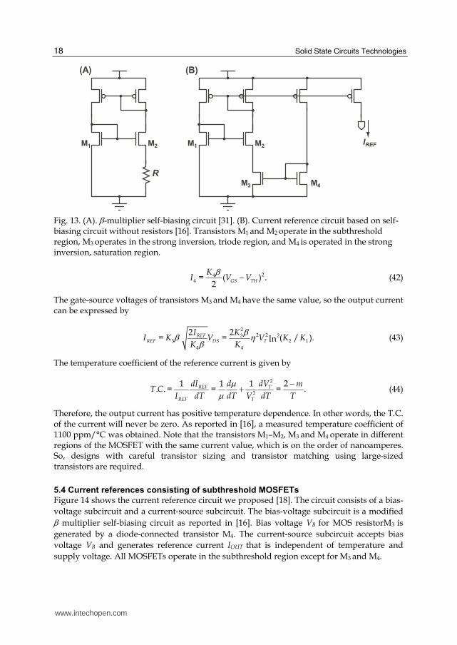
Figure13-(A) shows a β multiplier self-biasing circuit [31]. The circuit has a simple configuration and generates a PTAT current. However, the circuit requires large resistance of the resistor to reduce the operation current. To solve this problem, Oguey et al. developed
a modified β multiplier self-biasing circuit that uses a MOS resistor, M3, instead of ordinary resistors as shown in Fig. 13-(B) [16]. The gate-source voltage for MOS resistor M3 is generated by a diode-connected transistor M4. Transistors M1 and M2 operate in the subthreshold region. MOS resistor MR1 operates in a strong-inversion, deep-triode region, and the diode-connected transistor M4 operates in the strong-inversion, saturation region. The drain currents I3 and I4 in M3 and M4 are given by
3 3 3= ( ) ,GS TH DSI K V V Vβ − (41)
www.intechopen.com
Solid State Circuits Technologies
18
M1 M2
M3 M4
IREFM1 M2
R
(A) (B)
Fig. 13. (A). β-multiplier self-biasing circuit [31]. (B). Current reference circuit based on self-biasing circuit without resistors [16]. Transistors M1 and M2 operate in the subthreshold region, M3 operates in the strong inversion, triode region, and M4 is operated in the strong inversion, saturation region.
244 = ( ) .
2GS TH
KI V V
β − (42)
The gate-source voltages of transistors M3 and M4 have the same value, so the output current can be expressed by
2
2 2 233 2 1
4 4
2 2= = ( / ).ln
REFREF DS T
I KI K V V K K
K K
ββ ηβ (43)
The temperature coefficient of the reference current is given by
2
2
1 1 1 2. . = = = .REF T
REF T
dI d dV mT C
I dT dT V dT T
μμ
−+ (44)
Therefore, the output current has positive temperature dependence. In other words, the T.C. of the current will never be zero. As reported in [16], a measured temperature coefficient of 1100 ppm/°C was obtained. Note that the transistors M1–M2, M3 and M4 operate in different regions of the MOSFET with the same current value, which is on the order of nanoamperes. So, designs with careful transistor sizing and transistor matching using large-sized transistors are required.
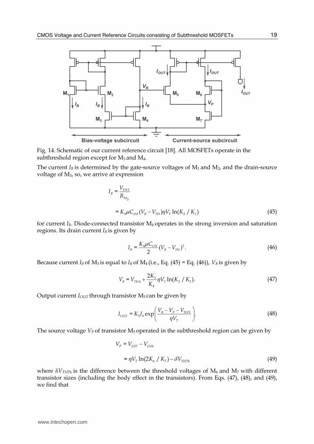
5.4 Current references consisting of subthreshold MOSFETs
Figure 14 shows the current reference circuit we proposed [18]. The circuit consists of a bias-
voltage subcircuit and a current-source subcircuit. The bias-voltage subcircuit is a modified
β multiplier self-biasing circuit as reported in [16]. Bias voltage VB for MOS resistorM3 is
generated by a diode-connected transistor M4. The current-source subcircuit accepts bias
voltage VB and generates reference current IOUT that is independent of temperature and
supply voltage. All MOSFETs operate in the subthreshold region except for M3 and M4.
www.intechopen.com
CMOS Voltage and Current Reference Circuits consisting of Subthreshold MOSFETs
19
M1 M2
M3 M4
M5 M6
M7
IOUT
VB
VP
Bias-voltage subcircuit Current-source subcircuit
IB IB IB
IOUT IOUT
Fig. 14. Schematic of our current reference circuit [18]. All MOSFETs operate in the subthreshold region except for M3 and M4.
The current IB is determined by the gate-source voltages of M1 and M2, and the drain-source voltage of M3, so, we arrive at expression
3
3
= DSB
M
VI
R
3 2 1= ( ) ln( / )OX B TH TK C V V V K Kμ η− (45)
for current IB. Diode-connected transistor M4 operates in the strong inversion and saturation regions. Its drain current IB is given by
24= ( ) .2
OXB B TH
K CI V V
μ − (46)
Because current IB of M3 is equal to IB of M4 (i.e., Eq. (45) = Eq. (46)), VB is given by
34 2 1
4
2= ln( / ).B TH T
KV V V K K
Kη+ (47)
Output current IOUT through transistor M5 can be given by
55 0= exp .B P TH
OUT
T
V V VI K I
Vη⎛ ⎞− −⎜ ⎟⎝ ⎠ (48)
The source voltage VP of transistor M5 operated in the subthreshold region can be given by
7 6=P GS GSV V V−
6 7 76= ln(2 / )T THV K K Vη δ− (49)
where VTH76 is the difference between the threshold voltages of M6 and M7 with different transistor sizes (including the body effect in the transistors). From Eqs. (47), (48), and (49), we find that
www.intechopen.com
Solid State Circuits Technologies
20
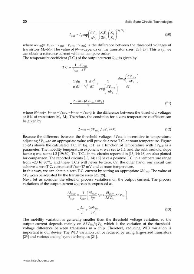
2 /3 4
5 7 20
6 1
= exp2
K K
THOUT
T
V K K KI I
V K K
δη
⎛ ⎞ ⎛ ⎞⎜ ⎟ ⎜ ⎟⎝ ⎠ ⎝ ⎠ (50)
where VTH(= VTH7 +VTH4 −VTH6 −VTH5) is the difference between the threshold voltages of transistors M4–M7. The value of VTH depends on the transistor sizes [28],[29]. This way, we can obtain a reference current with nanoampere-order. The temperature coefficient (T.C.) of the output current IOUT is given by
1
. . = OUT
OUT
dIT C
I dT
0
2
2
0
exp1 1 1
=
exp
TH
TT
T TH
T
Vd
Vd dV
dT V dT dTV
V
δημ
μ δη
⎛ ⎞⎜ ⎟⎝ ⎠+ + ⎛ ⎞⎜ ⎟⎝ ⎠
02 ( / )= TH Tm V V
T
δ η− − (51)
where VTH0(= VTH07 +VTH04 −VTH06 −VTH05) is the difference between the threshold voltages at 0 K of transistors M4–M7. Therefore, the condition for a zero temperature coefficient can be given by
02 ( / ) = 0.TH Tm V Vδ η− − (52)
Because the difference between the threshold voltages VTH0 is insensitive to temperature, adjusting VTH0 to an appropriate value will provide a zero T.C. at room temperature. Figure 15-(A) shows the calculated T.C. in Eq. (51) as a function of temperature with VTH0 as a parameter. The mobility temperature exponent m was set to 1.5, and the subthreshold slope factor η was set to 1.3 [19; 30]. The T.C.s in the circuits reported in [13; 14; 16] are also plotted for comparison. The reported circuits [13; 14; 16] have a positive T.C. in a temperature range from –20 to 80°C, and these T.C.s will never be zero. On the other hand, our circuit can achieve a zero T.C. current at VTH0=17 mV and at room temperature. In this way, we can obtain a zero T.C. current by setting an appropriate VTH0. The value of VTH0 can be adjusted by the transistor sizes [28; 29]. Next, let us consider the effect of process variations on the output current. The process variations of the output current IOUT can be expressed as
1=OUT OUT OUT
TH
OUT OUT TH
I I IV
I I Vμ δμ δ
⎛ ⎞Δ ∂ ∂Δ + Δ⎜ ⎟∂ ∂⎝ ⎠
= .TH
T
V
V
μ δμ ηΔ Δ+ (53)
The mobility variation is generally smaller than the threshold voltage variation, so the output current depends mainly on ΔVTH/ηVT, which is the variation of the threshold- voltage difference between transistors in a chip. Therefore, reducing WID variation is important in our device. The WID variation can be reduced by using large-sized transistors [23] and various analog layout techniques [24].
www.intechopen.com
CMOS Voltage and Current Reference Circuits consisting of Subthreshold MOSFETs
21
280 300 320 340 360
Temperature (K)
T.C.: Proposed
0
T.C
. (
10
-3/K
)
0.05
0.1
0.15
0.2
0.05
0 20 40 60 80Temperature ( C)
VDD
= 3.0 V
VDD
= 2.5 V
VDD
= 2.0 V
VDD
= 1.8 V
0 20 40 60 8090
92
94
96
98
100
I OU
T (
nA
)
Temperature ( C)
(A) (B)
T.C.: Oguey et. al. [16]T.C.: Sansen et. al. [14]
δVTH0
= 17 mV
δVTH0
= 16 mV
δVTH0
= 18 mV
T.C.: Ueno et. al. [13]
Fig. 15. (A). Calculated T.C.s of output currents as a function of temperature, with various VTH0; theoretical values obtained from Eqs. (31), (35), (44), and (51). (B). Measured output current IOUT as a function of temperature with various supply voltages. T.C. was 520 ppm/°C.
5.4.1 Experimental results
We fabricated a prototype chip using a 0.35-μm, 2-poly, 4-metal standard CMOS process, and we designed the circuit so as to produce a 100-nA output current. Figure 15-(B) shows measured output current IOUT as a function of temperature with supply voltage VDD as a parameter. The power supply voltage was set in a range from 1.8 to 3 V. The output current was about 96 nA and almost constant at temperatures in a range from 0 to 80°C. The temperature dependence and temperature coefficient were 50 pA/°C and 520 ppm/°C. An almost-constant reference current was obtained over a wide temperature range. The line regulation was 0.2%/V in a supply range of 1.8 to 3 V. Table II summarizes the characteristics of our device in comparison with other low-power CMOS current references reported in [13]-[18]. Our device is superior to others in chip area. In the circuits reported in [13]-[18], there are trade-offs between the power dissipations and the T.C. of the reference currents. Our device achieved an acceptable trade-off. The power dissipation of our device was 1 μW at a 1.8-V power supply, and the load regulation was 0.02%/V.
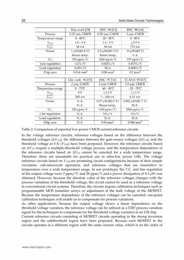
6. Conclusion and discussion
In this chapter, overviews of previous reported low-power reference circuits and details of our circuits were provided. These circuits generate constant reference voltages and currents that are independent of supply voltage and temperature. However, to achieve sub-microwatt operation in circuits that consist of MOSFETs and resistors, they require resistors with a high resistance of several hundred mega ohms. Such a high resistance needs a large area to be implemented, and this is quite inconvenient for practical use in ultra-low power LSIs. Therefore, reference circuits for sub-microwatt operation have to be implemented without the use of resistors.
www.intechopen.com
Solid State Circuits Technologies
22
Table 2. Comparison of reported low-power CMOS current reference circuits
In the voltage reference circuits, reference voltages based on the difference between the threshold voltages (ΔVTH), the difference between the gate-source voltages (ΔVGS), and the threshold voltage at 0 K (VTH0) have been proposed. However, the reference circuits based on ΔVTH require a multiple-threshold voltage process, and the temperature dependence of the reference circuits based on ΔVGS cannot be canceled for a wide temperature range. Therefore, these are unsuitable for practical use in ultra-low power LSIs. The voltage reference circuits based on VTH0 are promising circuit configurations because of their simple circuitries, sub-microwatt operation, and reference voltages that are insensitive to temperature over a wide temperature range. In our prototype, the T.C. and line regulation of the output voltage were 7 ppm/°C and 20 ppm/V and a power dissipation of 0.3 μW was obtained. However, because the absolute value of the reference voltages changes with the process variations of the threshold voltage, the circuit cannot be used as a reference voltage in conventional circuit systems. Therefore, the circuits require calibration techniques such as programmable MOS transistor arrays or adjustment of the bulk voltage of the MOSFET. Because the temperature dependence of the reference voltages can be canceled, one-point calibration techniques will enable us to compensate for process variations. As other applications, because the output voltage shows a linear dependence on the threshold voltage variation, the reference voltage can be utilized as a D2D process variation signal for the techniques to compensate for the threshold voltage variation in an LSI chip. Current reference circuits consisting of MOSFET circuits operating in the strong inversion region and the subthreshold region have been proposed. Because each MOSFET in the circuits operates in a different region with the same current value, which is on the order of
www.intechopen.com
CMOS Voltage and Current Reference Circuits consisting of Subthreshold MOSFETs
23
nanoamperes, careful transistor sizing and reducing WID variation in the design are important. The WID variation can be reduced by conventional circuit design techniques. In our circuit, techniques such as using large-sized transistors and common centroid layout were used to reduce the effect of the WID variation. From the theoretical results in the reported current references, the reference currents have a positive temperature dependence. Therefore, the circuits cannot be used as reference current circuits in environments with temperature changes. To solve this problem, we developed a temperature compensated current reference circuit with simple circuitry and a small area, and fabricated a prototype chip that generates a 100-nA output current. The T.C. and line regulation of the output current were 520 ppm/°C and 0.2%/V. A power dissipation of 1 μW was obtained. These circuits will be useful as voltage and current reference circuits for subthreshold-operated, power-aware LSI applications such as RFIDs, mobile devices, implantable medical devices, and smart sensor networks.
7. References
[1] K. Ueno, T. Hirose, T. Asai, and Y. Amemiya, “CMOS smart sensor for monitoring the quality of perishables,” IEEE Journal of Solid-State Circuits, vol. 42, no, 4, pp. 798-803, Apr. 2007.
[2] P. Fiorini, I. Doms, C. Van Hoof, R. Vullers, “Micropower energy scavenging,” Proc. of the 34th European Solid-State Circuits Conference (ESSCIRC), pp. 4-9, 2008.
[3] A. Wang, B.H. Clhoun, A.P. Chandracasan, Sub-threshold Design for Ultra Low-Power Systems, Springer, 2006.
[4] A. P. Chandrakasan, D. C. Daly, J. Kwong, Y. K. Ramadass, “Next Generation Micropower Systems,” Proc. of IEEE Symposium on VLSI Circuits, pp. 2-5, 2008.
[5] P. R. Gray and R. G. Meyer, Analysis and Design of Analog Integrated Circuits, 3rd ed. New York: Wiley, 1993.
[6] H. Banba, H. Shiga, A. Umezawa, T. Miyaba, T. Tanzawa, S. Atsumi, and K. Sakui, “A CMOS bandgap reference circuit with sub-1-V operation,” IEEE Journal of Solid-State Circuits, vol. 34, no. 5, pp. 670 - 674, May. 1999.
[7] B.-S. Song and P. R. Gray, “Threshold-voltage temperature drift in ion-implanted MOS transistors,” IEEE J. Solid-State Circuits, vol. SC-17, no. 2, pp. 291-298, Apr. 1982.
[8] K. N. Leung, P. K. T. Mok, “A CMOS voltage reference based on weighted ΔVGS for CMOS low-dropout linear regulators,” IEEE Journal of Solid-State Circuits, vol. 38, no. 1, pp. 146 - 150, Jan. 2003.
[9] G. De Vita, G. Iannaccone, P. Andreani, “A 300 nW, 12 ppm/°C Voltage Reference in a Digital 0.35 μm CMOS Process,” Dig. of Tech. Papers Symposium on VLSI Circuits. pp. 81-82, 2006.
[10] M.-H. Cheng, Z.-W. Wu, “Low-power low-voltage reference using peaking current mirror circuit,” Electronics Letters, vol. 41, no. 10, pp. 572 - 573, 2005.
[11] P-H. Huang, H. Lin, Y-T. Lin, “A simple subthreshold CMOS voltage reference circuit with channel-length modulation compensation,” IEEE Trans. Circuits Syst. II, Exp. Briefs, pp. 882 - 885, 2006.
[12] G. De Vita, G. Iannaccone, “A Sub-1-V, 10 ppm/°C, nanopower voltage reference generator” IEEE Journal of Solid-State Circuits, vol. 42, no. 7, pp. 1536 - 1542, Jul. 2007.
www.intechopen.com
Solid State Circuits Technologies
24
[13] K. Ueno, T. Hirose, T. Asai, Y. Amemiya, “A 300 nW, 15 ppm/°C, 20 ppm/V CMOS Voltage Reference Circuit Consisting of Subthreshold MOSFETs,” IEEE J. Solid-State Circuits, vol. 44, no. 7, pp. 2047-2054, Jul. 2009.
[14] W.M. Sansen, F. O. Eynde, M. Steyaert, “A CMOS temperaturecompensated current reference,” IEEE J. Solid-State Circuits, vol. 23, no. 3, pp. 821-824, Jun. 1988.
[15] C.-H. Lee, H.-J. Park, “All-CMOS temperature-independent current reference,” Electronics Letters, vol. 32, pp. 1280-1281, Jul. 1996.
[16] H. J. Oguey and D. Aebischer, “CMOS current reference without resistance,” IEEE J. Solid-State Circuits, vol. 32, no. 7, pp. 1132-1135, Jul. 1997.
[17] E. M. Camacho-Galeano and C. Galup-Montoro, “A 2-nW self-biased current reference in CMOS technology,” IEEE Trans. Circuits Syst. II, Exp. Briefs, vol. 52, no. 2, pp. 61-65, Feb. 2005.
[18] K. Ueno, T. Asai, Y. Amemiya, “Current reference circuit for subthreshold CMOS LSIs,” in Extended Abstract of Int. Conf. on Solid State Devices and Materials (SSDM), pp. 1000- 1001, 2008.
[19] Y. Taur, T.H. Ning, Fundamentals of Modern VLSI Devices, Cambridge University Press, 2002.
[20] I. M. Filanovsky, A. Allam, “Mutual compensation of mobility and threshold voltage temperature effects with applications in CMOS circuits,” IEEE Trans. Circuits Syst. I, Fundam. Theory Appl, pp. 876-884, 2001.
[21] K. A. Bowman, S. G. Duvall, J. D. Meindl, “Impact of die-to-die and within-die parameter fluctuations on the maximum clock frequency distribution for gigascale integration,” IEEE Journal of Solid-State Circuits, vol. 37, no. 2 pp. 183 - 190, Feb. 2002.
[22] H. Onodera, “Variability: Modeling and Its Impact on Design,” IEICE Trans. Electron., Vol.E89-C, pp. 342 - 348, 2006.
[23] M. J. M. Pelgrom, A. C. J. Duinmaijer, A. P. G. Welbers, “Matching properties of MOS transistors,” IEEE Journal of Solid-State Circuits, vol. 24, no. 5 pp. 1433 - 1439, Oct. 1989.
[24] A. Hastings, The Art of Analog Layout, Prentice Hall, 2001. [25] J. Chen, B. Shi, “1 V CMOS current reference with 50 ppm/°C temperature coefficient,”
Electronics Letters, vol. 39, no. 2, pp. 209-210, Jan. 2003. [26] B. Gilbert, “TRANSLINEAR CIRCUITS: A PROPOSED CLASSIFICATION,” Electronics
Letters, vol. 11, no. 1, pp. 15 - 16, 1975. [27] K. Ueno, T. Hirose, T. Asai, Y. Amemiya, “A 46-ppm/°C temperature and process
compensated current reference with on-chip threshold voltage monitoring circuit,” Proc. of the IEEE Asian Solid-State Circuits Conference (A-SSCC), pp. 161-164, 2008.
[28] M. C. Hsu, B. J. Sheu, “Inverse-geometry dependence of MOS transistor electrical parameters”, IEEE Trans. Computer-Aided Design, vol. CAD-6, pp. 582-585, July. 1987.
[29] Y. C. Cheng, M-C. Jeng, Z. Liu, J. H. Huang, M. Chen, K. Chen, P. K. Ko, C. Hu, “A physical and scalable IV model in BSIM3v3 for analog/digital circuit simulation.”, IEEE Trans. Electron Devices, vol. 44, No. 2, pp. 277-287, Feb. 1997.
[30] S. M. Sze, Physics of Semiconductor Devices, 2nd ed, John Wiley & Son, 1981. [31] Futaki H. A new type semiconductor (critical temperature resistor). Japan Journal of
Applied Physics, vol. 4, no. 1, pp. 28-41, 1965.
www.intechopen.com
Solid State Circuits TechnologiesEdited by Jacobus W. Swart
ISBN 978-953-307-045-2Hard cover, 462 pagesPublisher InTechPublished online 01, January, 2010Published in print edition January, 2010
InTech EuropeUniversity Campus STeP Ri Slavka Krautzeka 83/A 51000 Rijeka, Croatia Phone: +385 (51) 770 447 Fax: +385 (51) 686 166
InTech ChinaUnit 405, Office Block, Hotel Equatorial Shanghai No.65, Yan An Road (West), Shanghai, 200040, China
Phone: +86-21-62489820 Fax: +86-21-62489821
The evolution of solid-state circuit technology has a long history within a relatively short period of time. Thistechnology has lead to the modern information society that connects us and tools, a large market, and manytypes of products and applications. The solid-state circuit technology continuously evolves via breakthroughsand improvements every year. This book is devoted to review and present novel approaches for some of themain issues involved in this exciting and vigorous technology. The book is composed of 22 chapters, written byauthors coming from 30 different institutions located in 12 different countries throughout the Americas, Asiaand Europe. Thus, reflecting the wide international contribution to the book. The broad range of subjectspresented in the book offers a general overview of the main issues in modern solid-state circuit technology.Furthermore, the book offers an in depth analysis on specific subjects for specialists. We believe the book is ofgreat scientific and educational value for many readers. I am profoundly indebted to the support provided byall of those involved in the work. First and foremost I would like to acknowledge and thank the authors whoworked hard and generously agreed to share their results and knowledge. Second I would like to express mygratitude to the Intech team that invited me to edit the book and give me their full support and a fruitfulexperience while working together to combine this book.
How to referenceIn order to correctly reference this scholarly work, feel free to copy and paste the following:
Ken Ueno (2010). CMOS Voltage and Current Reference Circuits consisting of Subthreshold MOSFETs –Micropower Circuit Components for Power-Aware LSI Applications –, Solid State Circuits Technologies,Jacobus W. Swart (Ed.), ISBN: 978-953-307-045-2, InTech, Available from:http://www.intechopen.com/books/solid-state-circuits-technologies/cmos-voltage-and-current-reference-circuits-consisting-of-subthreshold-mosfets-micropower-circuit-co
www.intechopen.com

www.intechopen.com