
CMOS Comparators - ece.tamu.edujose-silva-martinez/courses/ECEN610/Comparat… · CMOS Comparators....
61
1 CMOS Comparators 1
Transcript of CMOS Comparators - ece.tamu.edujose-silva-martinez/courses/ECEN610/Comparat… · CMOS Comparators....

1
CMOS Comparators
1
2
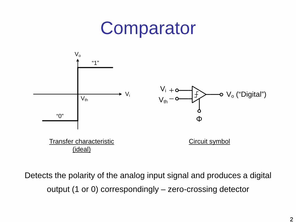
Comparator
Transfer characteristic(ideal)
Circuit symbol
Detects the polarity of the analog input signal and produces a digitaloutput (1 or 0) correspondingly – zero-crossing detector
Vi
Vo
“1”
“0”
Vth
Φ
Vi Vo (“Digital”)Vth
2
3
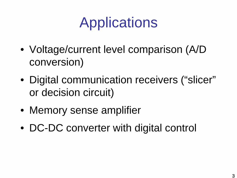
Applications
• Voltage/current level comparison (A/D conversion)
• Digital communication receivers (“slicer” or decision circuit)
• Memory sense amplifier• DC-DC converter with digital control
3
4
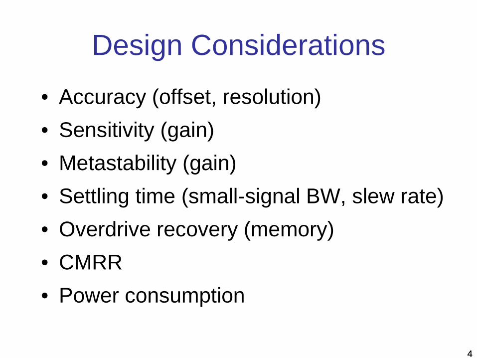
Design Considerations• Accuracy (offset, resolution)• Sensitivity (gain)• Metastability (gain)• Settling time (small-signal BW, slew rate)• Overdrive recovery (memory)• CMRR• Power consumption
4
5
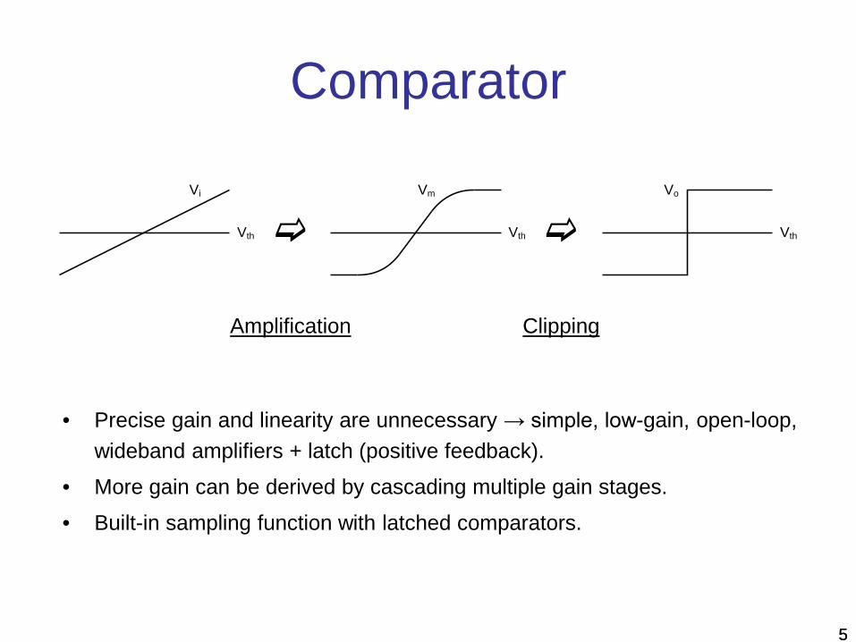
Comparator
Amplification Clipping
• Precise gain and linearity are unnecessary → simple, low-gain, open-loop,wideband amplifiers + latch (positive feedback).
• More gain can be derived by cascading multiple gain stages.• Built-in sampling function with latched comparators.
Vth
Vi
Vth
Vm
Vth
Vo
5
6
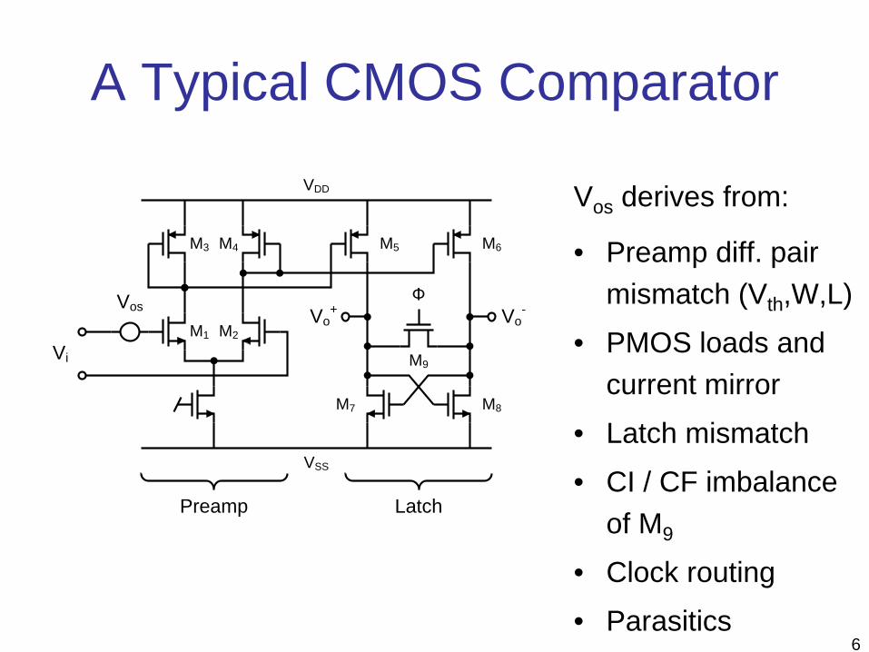
A Typical CMOS Comparator
Vos derives from:
• Preamp diff. pairmismatch (Vth,W,L)
• PMOS loads andcurrent mirror
• Latch mismatch• CI / CF imbalance
of M9
• Clock routing• Parasitics
M1 M2
Vi
Vos
M3 M4
VDD
M5 M6
M8M7
M9
VSS
ΦVo
+ Vo-
Preamp Latch
7
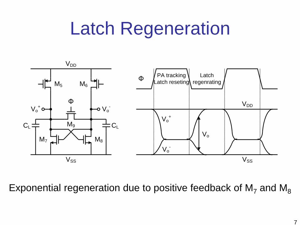
Latch Regeneration
Exponential regeneration due to positive feedback of M7 and M8
VDD
VSS
Vo
Φ PA tracking Latch reseting
Latchregenrating
Vo+
Vo-
VDD
M5 M6
M8M7
M9
VSS
ΦVo
+ Vo-
CL CL
8
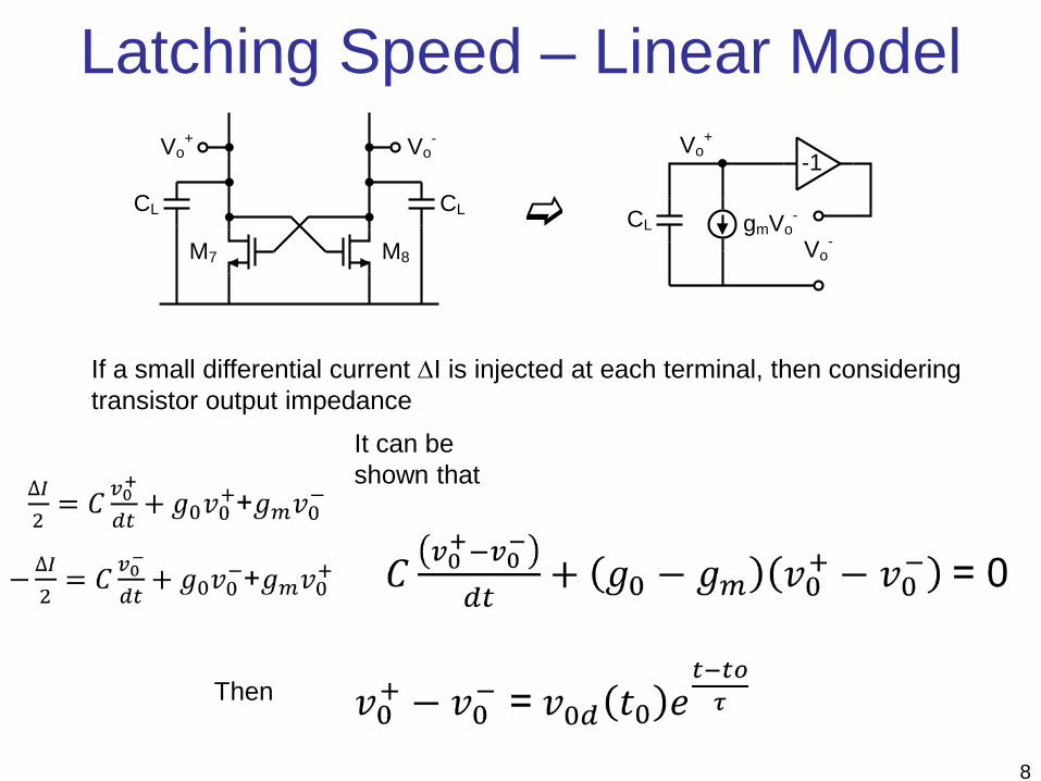
Latching Speed – Linear Model
M8M7
CL CL
Vo+ Vo
-
Vo-
Vo+
CL gmVo-
-1
If a small differential current ∆I is injected at each terminal, then considering transistor output impedance
It can be shown that
Then
9
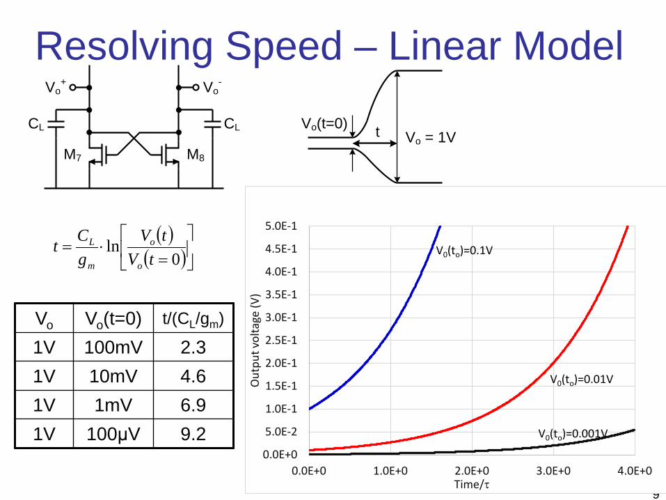
Resolving Speed – Linear Model
( )( )
=
⋅=0
lntV
tVgCt
o
o
m
L
M8M7
CL CL
Vo+ Vo
-
Vo = 1VVo(t=0) t
Vo Vo(t=0) t/(CL/gm)
1V 100mV 2.31V 10mV 4.61V 1mV 6.91V 100μV 9.2
0.0E+0
5.0E-2
1.0E-1
1.5E-1
2.0E-1
2.5E-1
3.0E-1
3.5E-1
4.0E-1
4.5E-1
5.0E-1
0.0E+0 1.0E+0 2.0E+0 3.0E+0 4.0E+0
Out
put v
olta
ge (V
)
Time/τ
V0(to)=0.1V
V0(to)=0.01V
V0(to)=0.001V
10
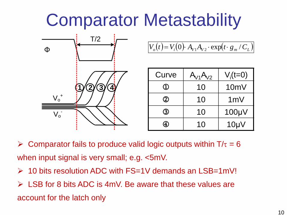
Comparator Metastability
Comparator fails to produce valid logic outputs within T/τ = 6 when input signal is very small; e.g. <5mV. 10 bits resolution ADC with FS=1V demands an LSB=1mV! LSB for 8 bits ADC is 4mV. Be aware that these values areaccount for the latch only
( ) ( ) ( )LmVVio CgtAAVtV /exp0 21 ⋅⋅⋅=
Curve AV1AV2 Vi(t=0) 10 10mV 10 1mV 10 100μV 10 10μV
Vo+
Φ
Vo-
1 2 3 4
T/2
11
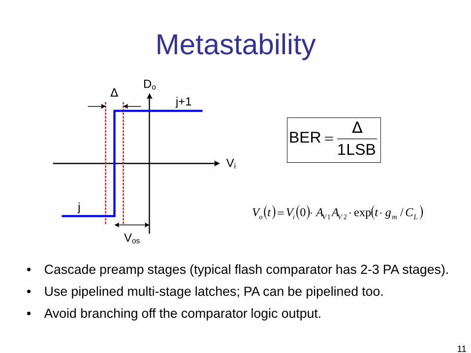
Metastability
• Cascade preamp stages (typical flash comparator has 2-3 PA stages).• Use pipelined multi-stage latches; PA can be pipelined too.• Avoid branching off the comparator logic output.
LSB1ΔBER =
( ) ( ) ( )LmVVio CgtAAVtV /exp0 21 ⋅⋅⋅=
Vi
DoΔ
j
Vos
j+1
12
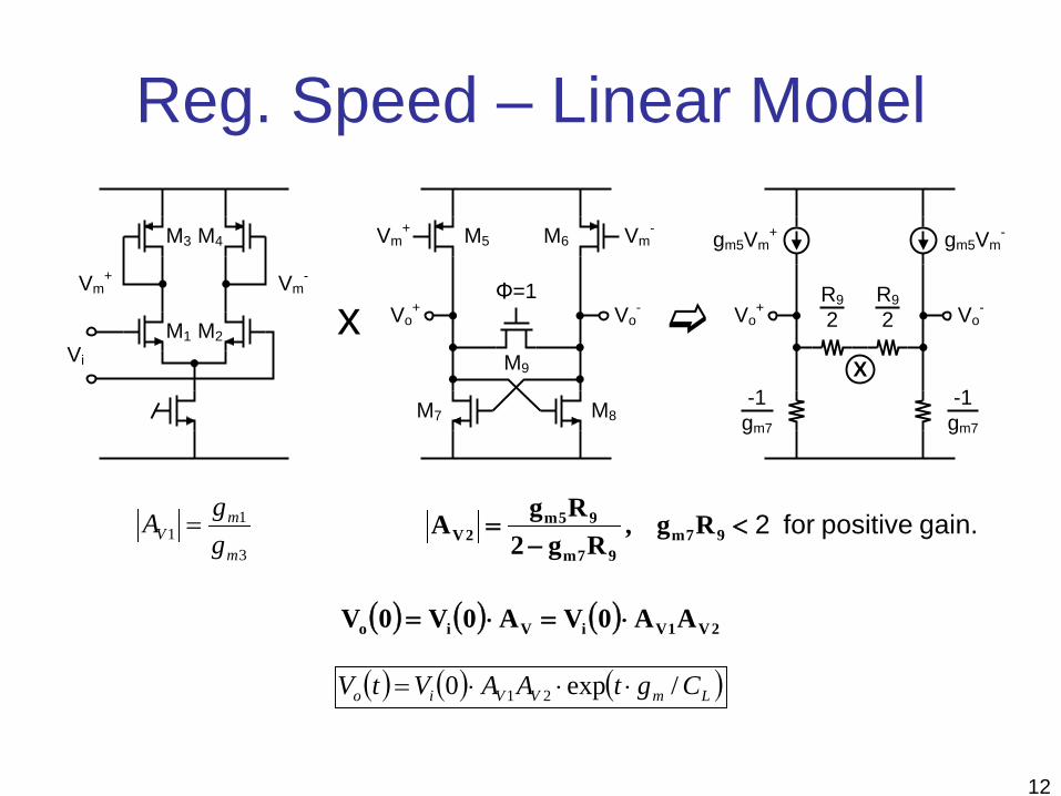
Reg. Speed – Linear Model
gain. positive for 2<−
= 97m97m
95m2V Rg
Rg2RgA ,
M5 M6
M8M7
M9
Φ=1Vo
+ Vo-
Vm+ Vm
-
M1 M2Vi
M3 M4
Vm+ Vm
-
Vo+ Vo
-R92
R92
-1gm7
-1gm7
gm5Vm+ gm5Vm
-
X
3
11
m
mV g
gA =
( ) ( ) ( ) 2V1ViVio AA0VA0V0V ⋅=⋅=
( ) ( ) ( )LmVVio CgtAAVtV /exp0 21 ⋅⋅⋅=
x
13
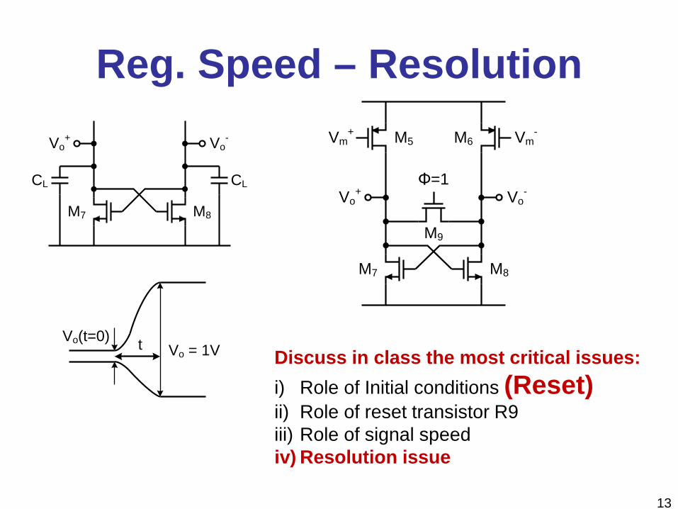
Reg. Speed – Resolution
M8M7
CL CL
Vo+ Vo
-
Vo = 1VVo(t=0) t
M5 M6
M8M7
M9
Φ=1Vo
+ Vo-
Vm+ Vm
-
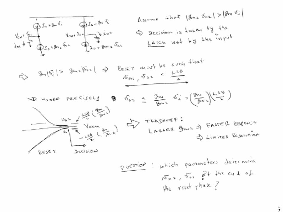
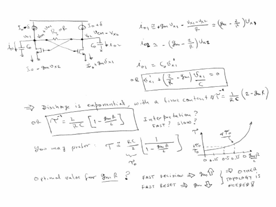
Discuss in class the most critical issues:i) Role of Initial conditions (Reset)ii) Role of reset transistor R9iii) Role of signal speediv) Resolution issue

14
Hysteresis: It should be < LSB/2
Vin
•Hysteresis: What the origin is?•Why this is relevant?•Design issues?•Design strategy (if any)?
I can anticipate that this is one of the most relevant issues when designing comparators
15
16
17
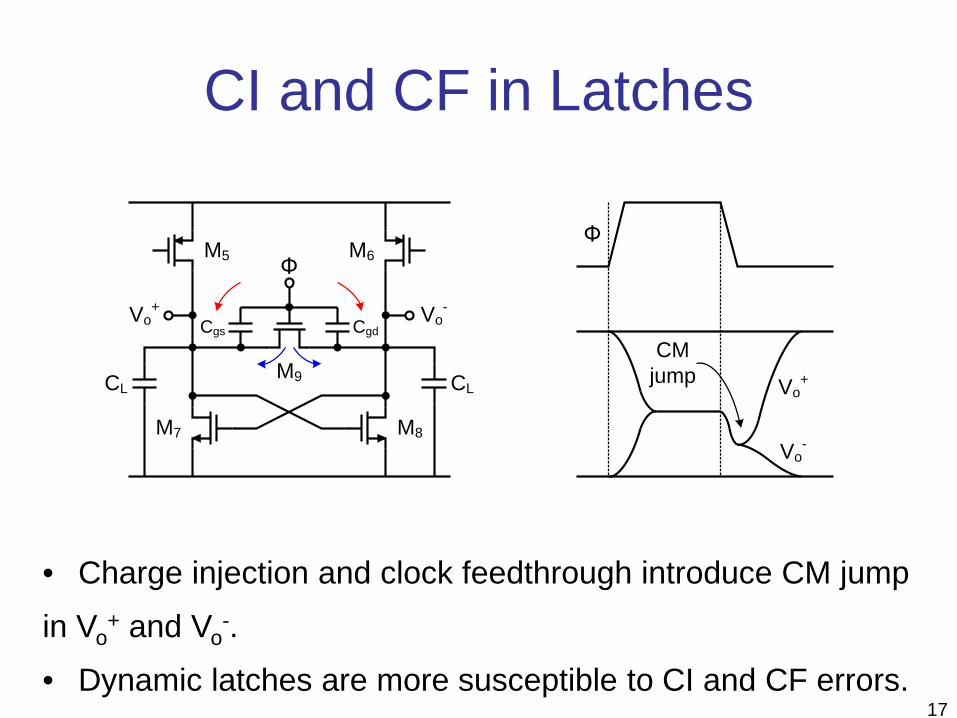
CI and CF in Latches
M5 M6
M8M7
Φ
Vo+ Vo
-
CL CLM9
CgdCgs
Vo+
Vo-
Φ
CM jump
• Charge injection and clock feedthrough introduce CM jump in Vo
+ and Vo-.
• Dynamic latches are more susceptible to CI and CF errors.
18
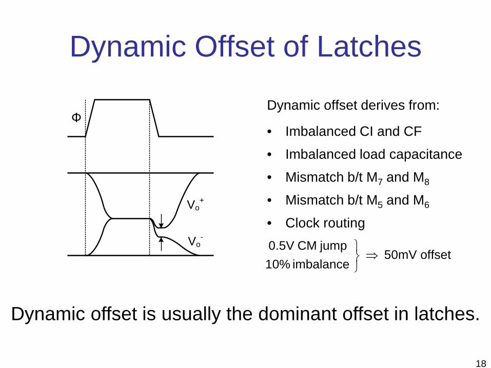
Dynamic Offset of Latches
Dynamic offset derives from:
• Imbalanced CI and CF• Imbalanced load capacitance• Mismatch b/t M7 and M8
• Mismatch b/t M5 and M6
• Clock routing
Φ
Vo+
Vo-
offset50mV imbalance 10%
jump CM0.5V ⇒
Dynamic offset is usually the dominant offset in latches.
19
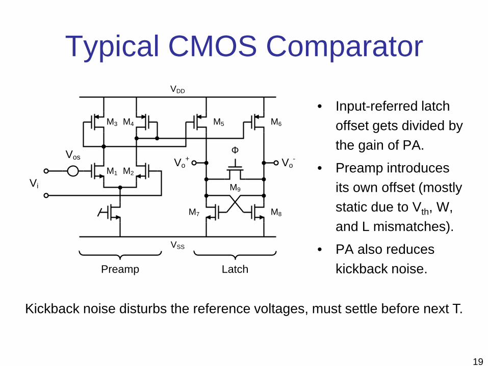
Typical CMOS Comparator
• Input-referred latchoffset gets divided bythe gain of PA.
• Preamp introducesits own offset (mostlystatic due to Vth, W,and L mismatches).
• PA also reduceskickback noise.
M1 M2
Vi
Vos
M3 M4
VDD
M5 M6
M8M7
M9
VSS
ΦVo
+ Vo-
Preamp Latch
Kickback noise disturbs the reference voltages, must settle before next T.

Fall 2009 S. Hoyos-ELEN-610 20
CMOS Preamplifier
21
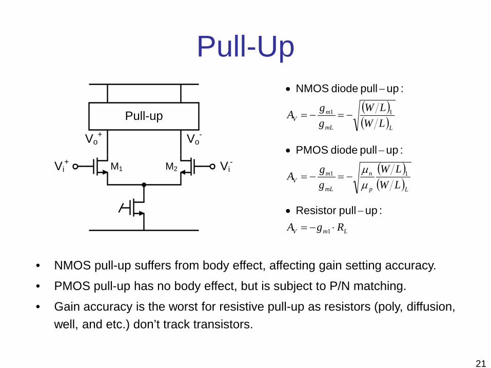
Pull-Up
• NMOS pull-up suffers from body effect, affecting gain setting accuracy.• PMOS pull-up has no body effect, but is subject to P/N matching.• Gain accuracy is the worst for resistive pull-up as resistors (poly, diffusion,
well, and etc.) don’t track transistors.
M1 M2Vi+ Vi
-
Vo+ Vo
-
Pull-up( )( )LmL
mV LW
LWggA 11 −=−=
−• :uppull diode NMOS
( )( )Lp
n
mL
mV LW
LWggA 11
µµ
−=−=
−• :uppull diode PMOS
LmV RgA ⋅−=−•
1
:uppull Resistor
22
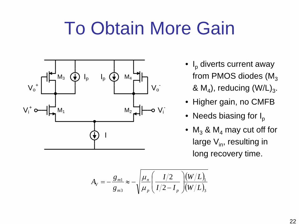
To Obtain More Gain
M1 M2
M3 M4
Vi+ Vi
-
Vo+ Vo
-Ip Ip
I
( )( )3
1
3
1
22
LWLW
III
ggA
pp
n
m
mV
−−≈−=
µµ
• Ip diverts current awayfrom PMOS diodes (M3
& M4), reducing (W/L)3.• Higher gain, no CMFB• Needs biasing for Ip• M3 & M4 may cut off for
large Vin, resulting inlong recovery time.
23
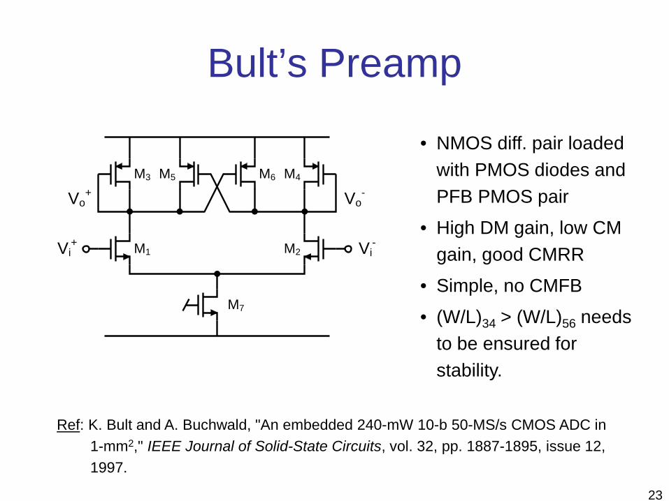
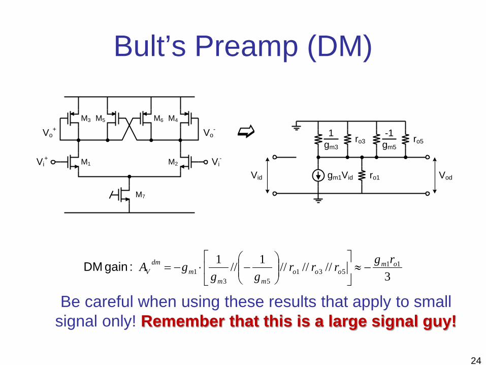
Bult’s Preamp
• NMOS diff. pair loadedwith PMOS diodes andPFB PMOS pair
• High DM gain, low CMgain, good CMRR
• Simple, no CMFB• (W/L)34 > (W/L)56 needs
to be ensured forstability.
Ref: K. Bult and A. Buchwald, "An embedded 240-mW 10-b 50-MS/s CMOS ADC in1-mm2," IEEE Journal of Solid-State Circuits, vol. 32, pp. 1887-1895, issue 12,1997.
M1 M2
M7
M3 M4
Vi+ Vi
-
Vo+ Vo
-M5 M6
24
Bult’s Preamp (DM)
Vid gm1Vid ro1
1gm3
ro3-1
gm5ro5
Vod
3//////1//1 11
53153
1om
ooomm
mdm
Vrgrrr
gggA −≈
−⋅−= :gain DM
M1 M2
M7
M3 M4
Vi+ Vi
-
Vo+ Vo
-M5 M6
Be careful when using these results that apply to small signal only! Remember that this is a large signal guy!
25
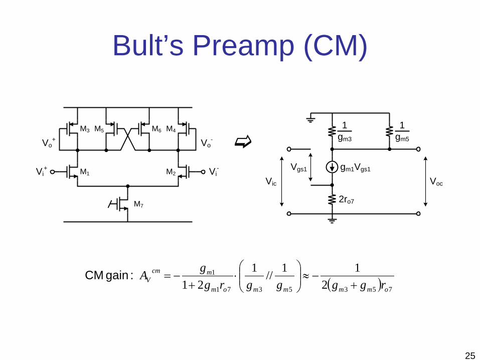
Bult’s Preamp (CM)
( ) 7535371
1
211//1
21 ommmmom
mcmV rggggrg
gA+
−≈
⋅
+−= :gain CM
Vic
gm1Vgs1
2ro7
1gm3
1gm5
Voc
Vgs1M1 M2
M7
M3 M4
Vi+ Vi
-
Vo+ Vo
-M5 M6
26
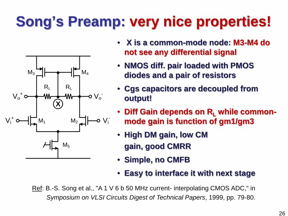
Song’s Preamp: very nice properties!
Ref: B.-S. Song et al., "A 1 V 6 b 50 MHz current- interpolating CMOS ADC," inSymposium on VLSI Circuits Digest of Technical Papers, 1999, pp. 79-80.
M1 M2
M5
M4M3
Vi+ Vi
-
Vo+ Vo
-RL RL
X
• X is a common-mode node: M3-M4 do not see any differential signal
• NMOS diff. pair loaded with PMOS diodes and a pair of resistors
• Cgs capacitors are decoupled from output!
• Diff Gain depends on RL while common-mode gain is function of gm1/gm3
• High DM gain, low CMgain, good CMRR
• Simple, no CMFB• Easy to interface it with next stage
27
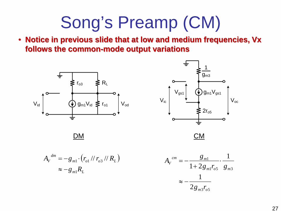
Song’s Preamp (CM)
53
351
1
21
121
om
mom
mcmV
rg
grggA
−≈
⋅+
−=
Vid gm1Vid ro1
ro3 RL
VodVic
gm1Vgs1
2ro5
1gm3
Voc
Vgs1
DM CM
( )Lm
Loomdm
V
RgRrrgA
1
311 ////−≈
⋅−=
• Notice in previous slide that at low and medium frequencies, Vxfollows the common-mode output variations

28
CMOS Latch
29
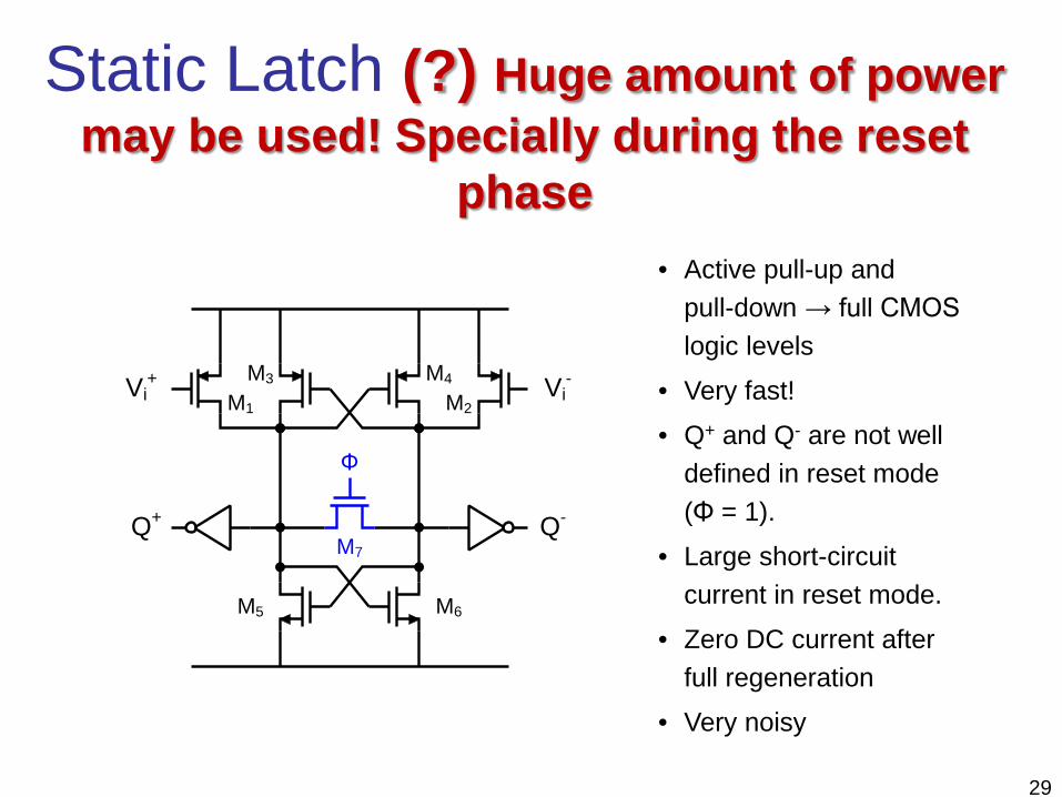
Static Latch (?) Huge amount of power may be used! Specially during the reset
phase• Active pull-up and
pull-down → full CMOSlogic levels
• Very fast!• Q+ and Q- are not well
defined in reset mode(Φ = 1).
• Large short-circuitcurrent in reset mode.
• Zero DC current afterfull regeneration
• Very noisy
M6M5
M7Q+ Q-
Φ
Vi+ Vi
-M1 M2
M3 M4
30
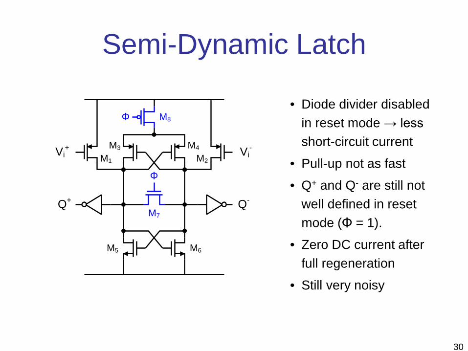
Semi-Dynamic Latch
• Diode divider disabledin reset mode → lessshort-circuit current
• Pull-up not as fast• Q+ and Q- are still not
well defined in resetmode (Φ = 1).
• Zero DC current afterfull regeneration
• Still very noisy
M6M5
M7
Φ
Φ
M8
Vi+ Vi
-M1 M2
M3 M4
Q+ Q-
31
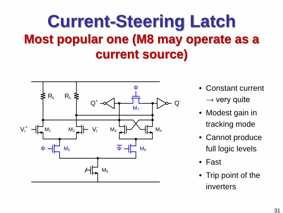
Current-Steering LatchMost popular one (M8 may operate as a
current source)
• Constant current→ very quite
• Modest gain intracking mode
• Cannot producefull logic levels
• Fast• Trip point of the
inverters
M1 M2
M5
Vi+
M6
Vi- M4M3
M7
Φ
M8
Φ Φ
RL RLQ+ Q-
32
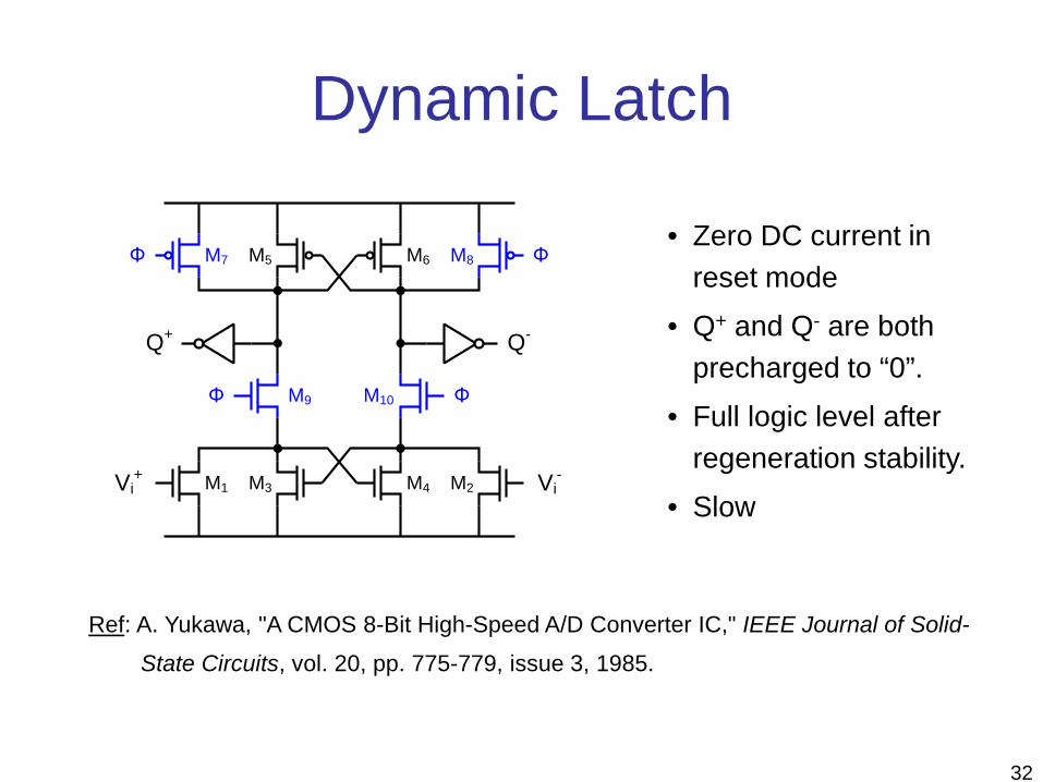
Dynamic Latch
• Zero DC current inreset mode
• Q+ and Q- are bothprecharged to “0”.
• Full logic level afterregeneration stability.
• Slow
Ref: A. Yukawa, "A CMOS 8-Bit High-Speed A/D Converter IC," IEEE Journal of Solid-
State Circuits, vol. 20, pp. 775-779, issue 3, 1985.
M4M3
Φ
Vi+ Vi
-
M7 M8M5 M6
M1
Q+ Q-
M2
M9 M10 Φ
ΦΦ
33
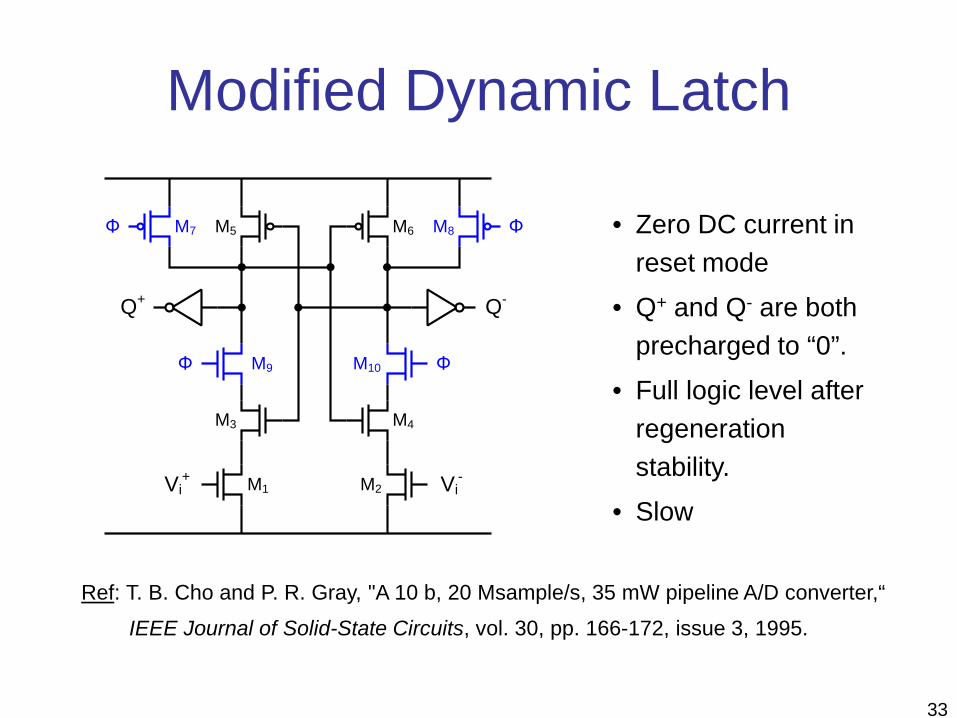
Modified Dynamic Latch
Ref: T. B. Cho and P. R. Gray, "A 10 b, 20 Msample/s, 35 mW pipeline A/D converter,“IEEE Journal of Solid-State Circuits, vol. 30, pp. 166-172, issue 3, 1995.
Φ
Vi+ Vi
-
M7 M8M5 M6
M1
Q+ Q-
M2
M9 M10 Φ
ΦΦ
M4M3
• Zero DC current inreset mode
• Q+ and Q- are bothprecharged to “0”.
• Full logic level afterregenerationstability.
• Slow
34
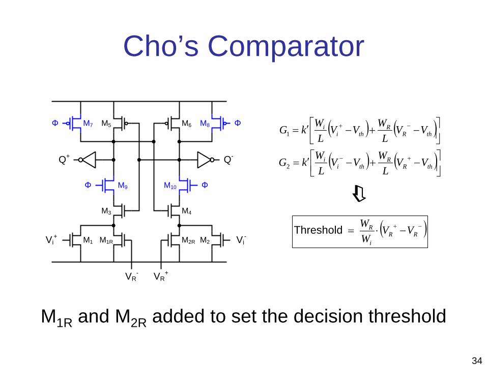
Cho’s Comparator
M1R and M2R added to set the decision threshold
( ) ( )
( ) ( )
−+−′=
−+−′=
+−
−+
thRR
thii
thRR
thii
VVL
WVVL
WkG
VVL
WVVL
WkG
2
1
( )−+ −⋅= RRi
R VVWWThreshold
M2RM1R
Φ
Vi+ Vi
-
M7 M8M5 M6
M1
Q+ Q-
M2
M9 M10 Φ
ΦΦ
M4M3
VR- VR
+
35
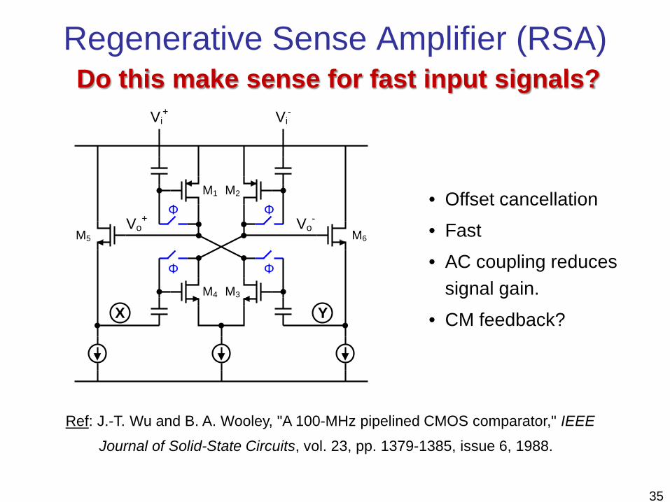
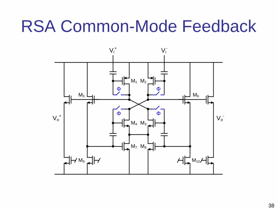
Regenerative Sense Amplifier (RSA)
Ref: J.-T. Wu and B. A. Wooley, "A 100-MHz pipelined CMOS comparator," IEEE
Journal of Solid-State Circuits, vol. 23, pp. 1379-1385, issue 6, 1988.
• Offset cancellation• Fast• AC coupling reduces
signal gain.• CM feedback?
Vi+ Vi
-
M1 M2
M4 M3
M6M5
Φ Φ
Φ Φ
X Y
Vo+ Vo
-
Do this make sense for fast input signals?
36
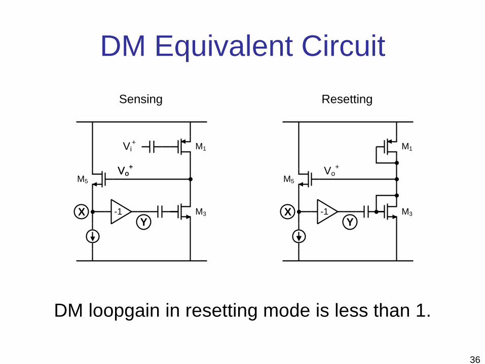
DM Equivalent Circuit
M1
M3
M5
X
Vo+
-1Y
Vi+
M5
X
Vo+
M1
M3
Vo+
-1Y
Sensing Resetting
DM loopgain in resetting mode is less than 1.
37
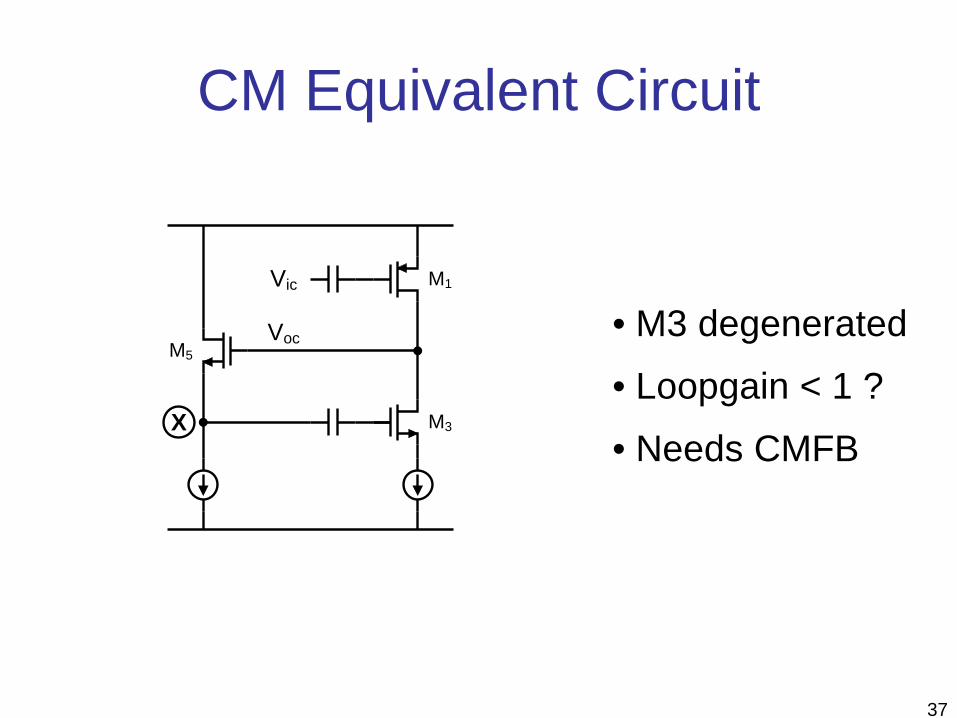
CM Equivalent Circuit
Vic
M5
X
M1
M3
Voc • M3 degenerated• Loopgain < 1 ?• Needs CMFB
38
RSA Common-Mode FeedbackVi
+ Vi-
M1 M2
M4 M3
M6M5
Φ Φ
Φ Φ
M7
M10M9
Vo+ Vo
-
M8
39
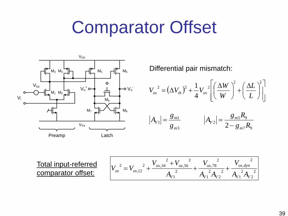
Comparator Offset
M1 M2
Vi
Vos
M3 M4
VDD
M5 M6
M8M7
M9
VSS
ΦVo
+ Vo-
Preamp Latch
( )
∆+
∆+∆=
22222
41
LL
WWVVV ovthos
97
952 2 Rg
RgAm
mV −
=3
11
m
mV g
gA =
22
21
2,
22
21
278,
21
256,
234,2
12,2
VV
dynos
VV
os
V
osososos AA
VAA
VA
VVVV ++
++=
Differential pair mismatch:
Total input-referredcomparator offset:

40
Matching Properties
( ) ,222
2 DSWLAP P
P +=∆σ
The variance of parameter ΔP b/t two rectangular devices:
where, W and L are the effective width and length, Sp stands for the technology sensitivity to distance and orientation; D is distance between the devices.
Ref: M. J. M. Pelgrom, et al., "Matching properties of MOS transistors,"IEEE Journal of Solid-State Circuits, vol. 24, pp. 1433-1439, issue 5, 1989.
( )
( ) .
,
222
2
2
220
20
02
DSWLA
DSWLAV VT
VTT
ββ
ββσ
σ
+=
+=
:factor Current
:Threshold
1st term dominatesfor small devices.

41
Why Large Devices Match Better?
., 11 RS WLRR σ std with⋅=
X X X X X X X X…W
L10 identical resistors
R1 R2
.11101
1010
1
1
1
1
2
2
WLARRRRRRRR =∝⇒
==
σσσσ
.1010
,,1010
122
1
10
1
222
212
RRRj
RR
RS
j
RWLRR
σσσσσ
σ
=⇒==
=
⋅=
∑=
std with
“Spatialaveraging”
42
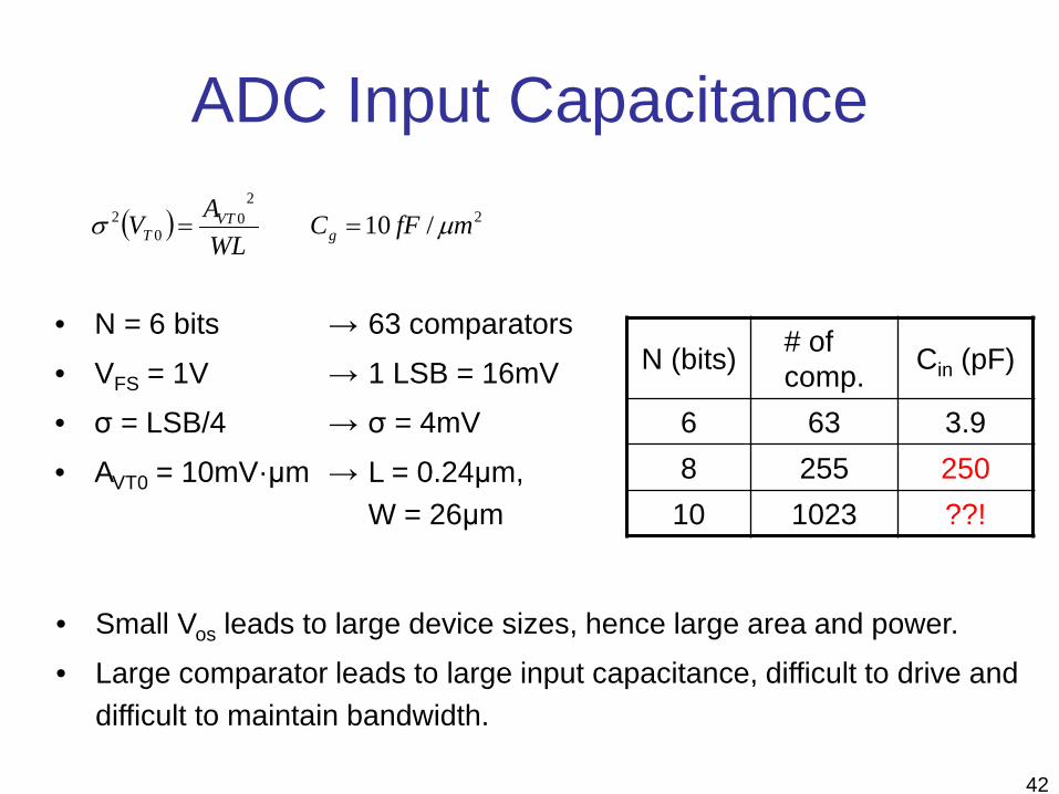
ADC Input Capacitance
( ) 22
00
2 /10 mfFCWLAV g
VTT µσ ==
• N = 6 bits• VFS = 1V• σ = LSB/4• AVT0 = 10mV·μm
→ 63 comparators→ 1 LSB = 16mV→ σ = 4mV→ L = 0.24μm,
W = 26μm
N (bits) # of comp. Cin (pF)
6 63 3.98 255 250
10 1023 ??!
• Small Vos leads to large device sizes, hence large area and power.• Large comparator leads to large input capacitance, difficult to drive and
difficult to maintain bandwidth.
43
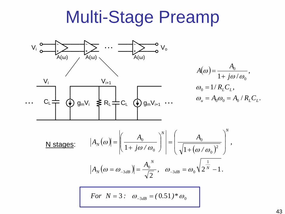
Multi-Stage Preamp
A(ω)
Vi
A(ω) A(ω)
… Vo
Vi
CL gmVi CLRL gmVi+1
Vi+1
… …
( )
./,/1
,/1
000
0
0
0
LLu
LL
CRAACRjAA
===
+=
ωωω
ωωω
( )( )
( )
03
1
030
3
20
0
0
0
5103
122
11
ωω
ωωωω
ωωωωω
*).(:NFor
.,A
A
,/
A/j
AA
dB
NdB
N
dBN
NN
N
==
−===
+=
+
=
−
−−
N stages:
44
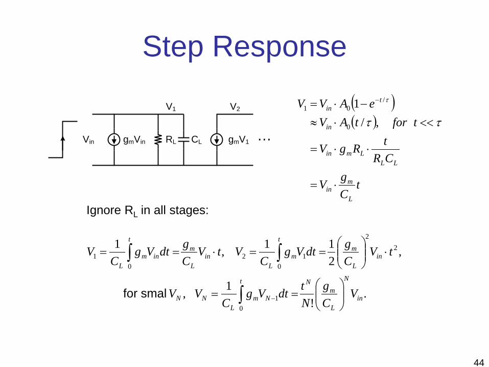
Step Response
( )( )
tCgV
CRtRgV
tfortAVeAVV
L
min
LLLmin
in
tin
⋅=
⋅⋅=
<<⋅≈−⋅= −
ττ
τ
,/1
0
/01
.!
1,
,211,1
01
22
012
01
in
N
L
mNt
NmL
NN
inL
mt
mL
inL
mt
inmL
VCg
NtdtVg
CVV
tVCgdtVg
CVtV
CgdtVg
CV
==
⋅
==⋅==
∫
∫∫
− smal for
Ignore RL in all stages:
Vin gmVin CLRL gmV1
V1
…
V2
45
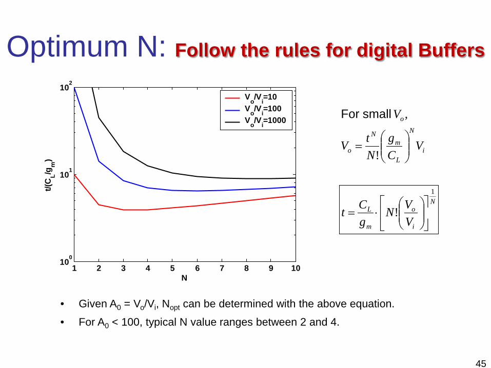
Optimum N: Follow the rules for digital Buffers
i
N
L
mN
o
o
VCg
NtV
,V
=
!
small For
1 2 3 4 5 6 7 8 9 10100
101
102
N
t/(C
L/gm
)
Vo/Vi=10Vo/Vi=100Vo/Vi=1000
N
i
o
m
L
VVN
gCt
1
!
⋅=
• Given A0 = Vo/Vi, Nopt can be determined with the above equation.• For A0 < 100, typical N value ranges between 2 and 4.
46
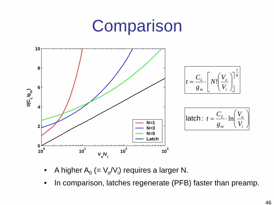
Comparison
• A higher A0 (= Vo/Vi) requires a larger N.• In comparison, latches regenerate (PFB) faster than preamp.
⋅=
i
o
m
L
VV
gCt ln :latch
N
i
o
m
L
VVN
gCt
1
!
⋅=
100 101 102 1030
2
4
6
8
10
Vo/Vi
t/(C
L/gm
)
N=1N=3N=5Latch
47
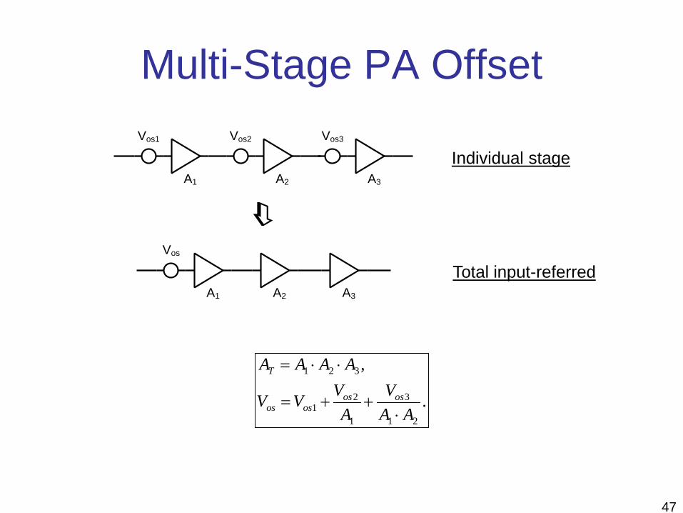
Multi-Stage PA Offset
Total input-referred
Individual stage
A1
Vos1
A2
Vos2
A3
Vos3
A1
Vos
A2 A3
.
,
21
3
1
21
321
AAV
AVVV
AAAA
osososos
T
⋅++=
⋅⋅=
48
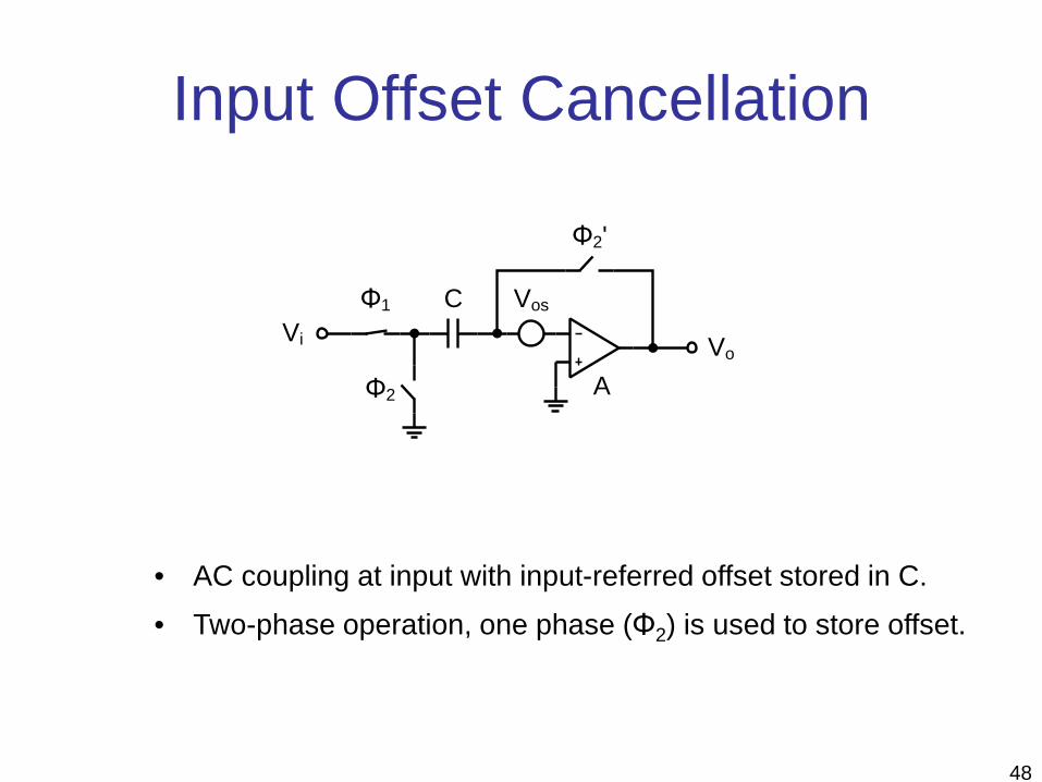
Input Offset Cancellation
A
VosΦ1
Φ2
Φ2'
Vi Vo
C
• AC coupling at input with input-referred offset stored in C.• Two-phase operation, one phase (Φ2) is used to store offset.
49
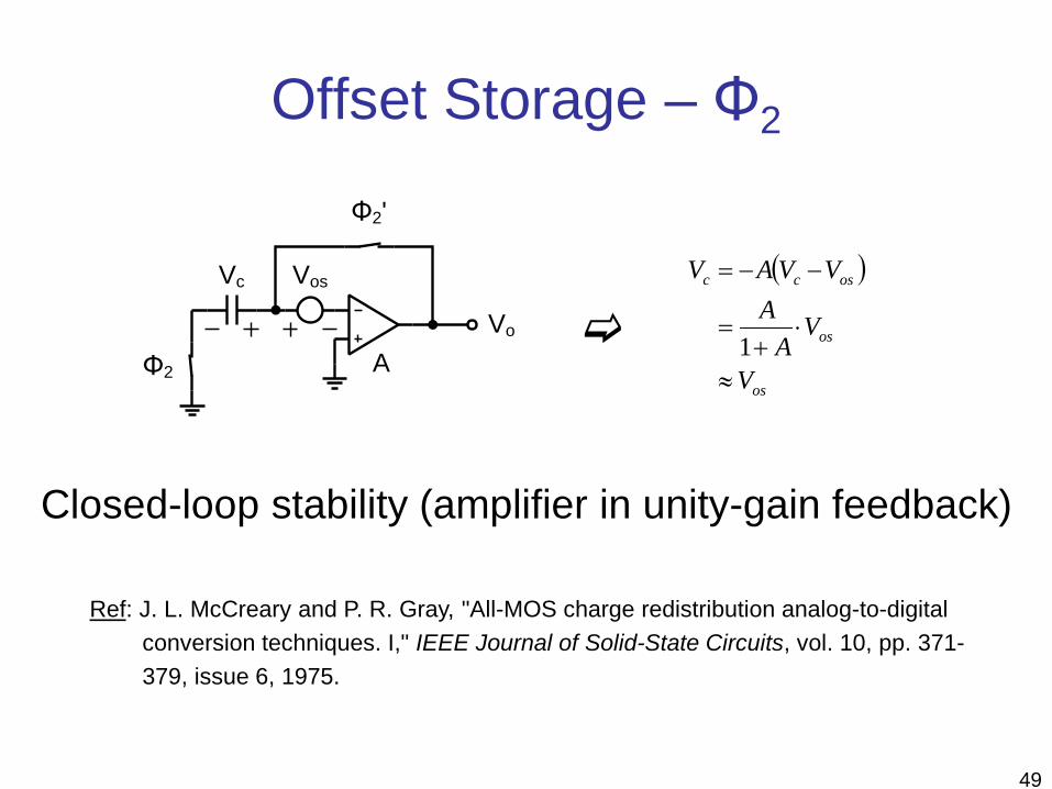
Offset Storage – Φ2
( )
os
os
oscc
V
VA
AVVAV
≈
⋅+
=
−−=
1A
Vos
Φ2
Φ2'
Vo
Vc
Closed-loop stability (amplifier in unity-gain feedback)
Ref: J. L. McCreary and P. R. Gray, "All-MOS charge redistribution analog-to-digitalconversion techniques. I," IEEE Journal of Solid-State Circuits, vol. 10, pp. 371-379, issue 6, 1975.
50
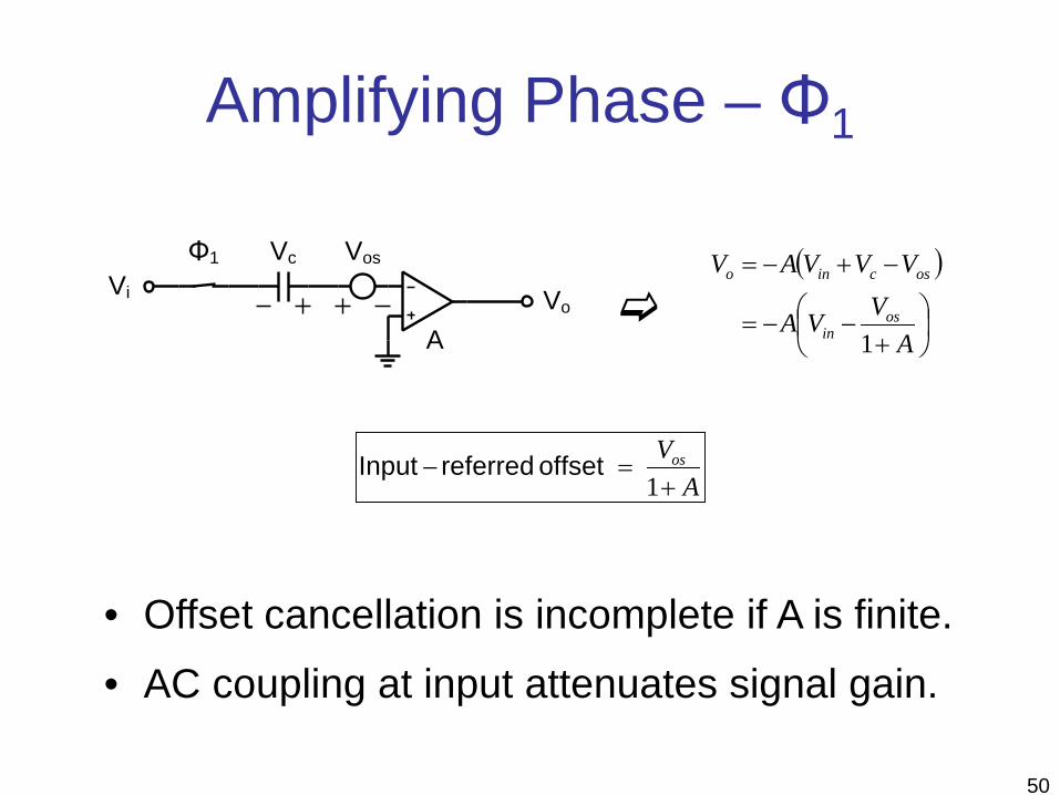
Amplifying Phase – Φ1
( )
+−−=
−+−=
AVVA
VVVAV
osin
oscino
1
• Offset cancellation is incomplete if A is finite.• AC coupling at input attenuates signal gain.
AVos
+=−
1 offset referredInput
A
VosΦ1
Vi Vo
Vc
51
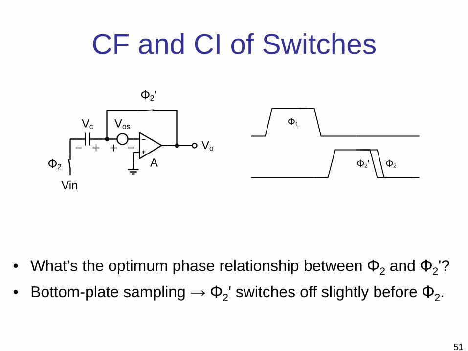
CF and CI of Switches
A
Vos
Φ2
Φ2'
Vo
Vc
• What’s the optimum phase relationship between Φ2 and Φ2'?• Bottom-plate sampling → Φ2' switches off slightly before Φ2.
Φ2'
Φ1
Φ2
Vin
52
Multi-Stage Input Offset Cancellation
A1
Vos1Φ1
Φ2
Φ3
Vi
C1
A2
Vos2
Φ4
Vo
C2
Φ1
Φ2
Φ3
Φ4
• Multi-stage AC coupling• Φ3 switches off first
→ ΔV1 on C1 will beabsorbed by C2.
• Φ4 switches off next, Φ2
last.
53
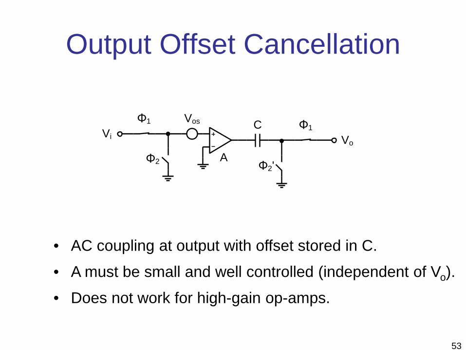
Output Offset Cancellation
• AC coupling at output with offset stored in C.• A must be small and well controlled (independent of Vo).• Does not work for high-gain op-amps.
A
VosΦ1
Φ2
Vi Vo
C Φ1
Φ2'
54
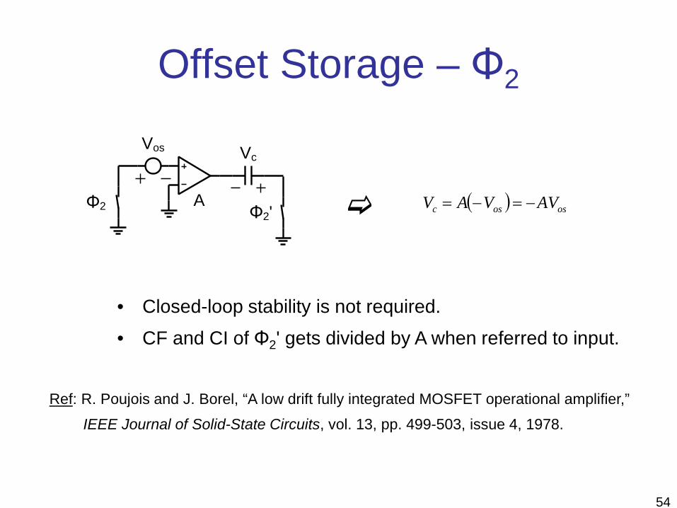
Offset Storage – Φ2
( ) ososc AVVAV −=−=
• Closed-loop stability is not required.• CF and CI of Φ2' gets divided by A when referred to input.
Ref: R. Poujois and J. Borel, “A low drift fully integrated MOSFET operational amplifier,”IEEE Journal of Solid-State Circuits, vol. 13, pp. 499-503, issue 4, 1978.
Vos
Φ2
Vc
Φ2'A
55
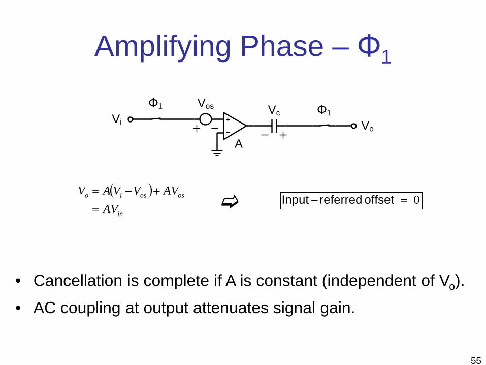
Amplifying Phase – Φ1
( )
in
ososio
AVAVVVAV
=+−=
• Cancellation is complete if A is constant (independent of Vo).• AC coupling at output attenuates signal gain.
0=− offset referredInput
VosΦ1
Vi Vo
Vc Φ1
A
56
Multi-Stage Output Offset Cancellation
Φ1
Φ2
Φ3
Φ4
• Multi-stage AC coupling• Φ3 switches off first
→ ΔV1 on C1 will beabsorbed by C2.
• Φ4 switches off next, Φ2
last.
A1
Vos1Φ1
Φ2
ViVo
C1
Φ3 A2
Vos2 C2
Φ4

57
Overdrive Recovery
58
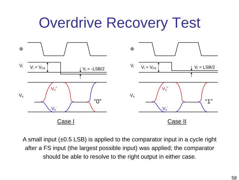
Overdrive Recovery Test
A small input (±0.5 LSB) is applied to the comparator input in a cycle rightafter a FS input (the largest possible input) was applied; the comparator
should be able to resolve to the right output in either case.
Φ
Vo+
Vo-
Vi
Vo
Vi = VFS Vi = -LSB/2
Φ
Vo+
Vo-
Vi
Vo
Vi = VFS Vi = LSB/2
“0” “1”
Case I Case II
59
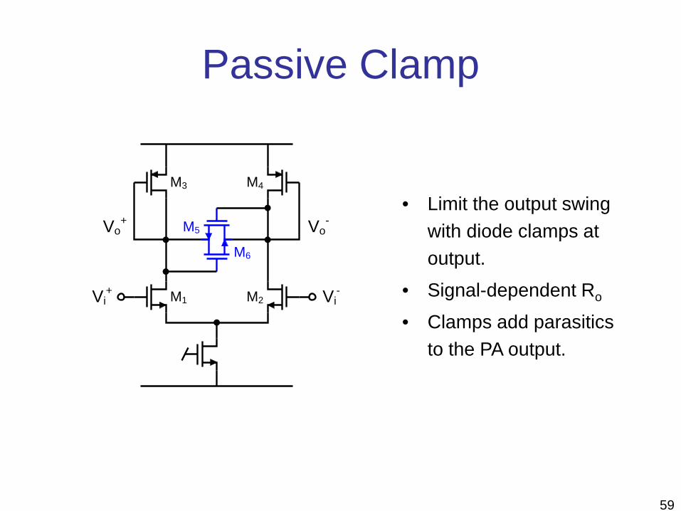
Passive Clamp
• Limit the output swingwith diode clamps atoutput.
• Signal-dependent Ro
• Clamps add parasiticsto the PA output.
M1 M2
M3 M4
Vi+ Vi
-
M6
M5Vo+ Vo
-
60
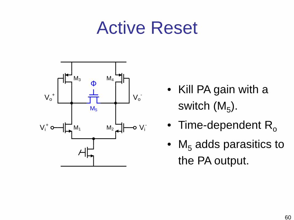
Active Reset
• Kill PA gain with aswitch (M5).
• Time-dependent Ro
• M5 adds parasitics tothe PA output.
M1 M2
M3 M4
Vi+ Vi
-
M5
Vo+ Vo
-
Φ
61
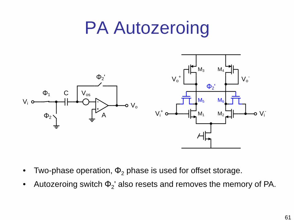
PA Autozeroing
A
VosΦ1
Φ2
Φ2'
Vi Vo
C
• Two-phase operation, Φ2 phase is used for offset storage.• Autozeroing switch Φ2' also resets and removes the memory of PA.
M1 M2
M3 M4
Vi+ Vi
-
M5
Vo+ Vo
-
Φ2'
M6


![Adaptive CMOS Circuits for 4G Wireless Networksdigital.csic.es/bitstream/10261/3754/1/ECCTD07_TutorialJrosa.pdf · Adaptive CMOS Circuits for 4G Wireless Networks ... [UMTS/WCDMA]](https://static.fdocument.org/doc/165x107/5ae0f6c27f8b9af05b8e5633/adaptive-cmos-circuits-for-4g-wireless-cmos-circuits-for-4g-wireless-networks-.jpg)


![Power Efficient CMOS Full Adders with Reduced Transistor Count · The TGA full adder [5] using 20 transistors is based on CMOS transmission gates and CMOS inverters. It ... In TFA](https://static.fdocument.org/doc/165x107/5c01a10709d3f20f068d0c17/power-efficient-cmos-full-adders-with-reduced-transistor-count-the-tga-full.jpg)