CINT1175 REV 5.3, 12-June-13 - SL Power Electronics
9
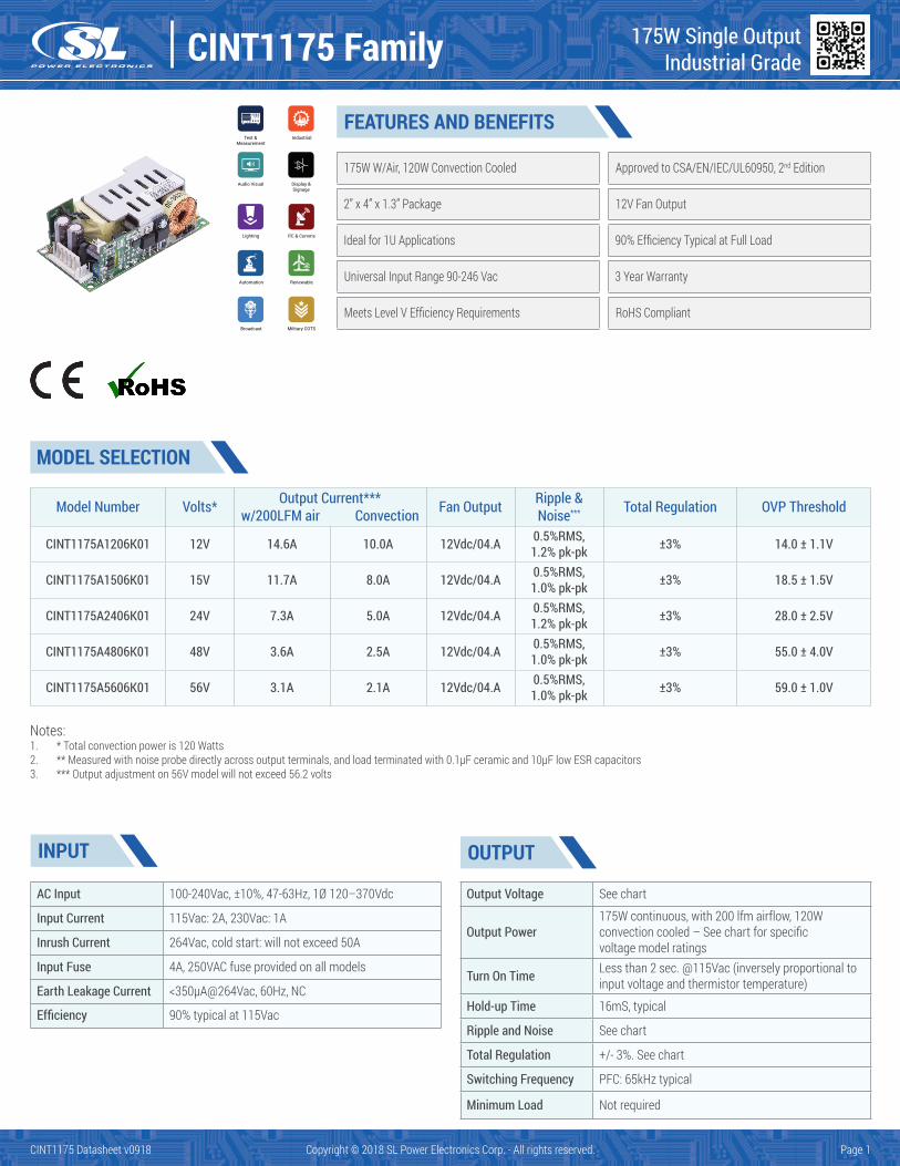
CINT1175 Family 175W Single Output Industrial Grade Page 1 CINT1175 Datasheet v0918 Copyright © 2018 SL Power Electronics Corp. - All rights reserved. Notes: 1. * Total convection power is 120 Watts 2. ** Measured with noise probe directly across output terminals, and load terminated with 0.1μF ceramic and 10μF low ESR capacitors 3. *** Output adjustment on 56V model will not exceed 56.2 volts Approved to CSA/EN/IEC/UL60950, 2 nd Edition 12V Fan Output 90% Efficiency Typical at Full Load 3 Year Warranty RoHS Compliant 175W W/Air, 120W Convection Cooled 2” x 4” x 1.3” Package Ideal for 1U Applications Universal Input Range 90-246 Vac Meets Level V Efficiency Requirements FEATURES AND BENEFITS MODEL SELECTION AC Input 100-240Vac, ±10%, 47-63Hz, 1Ø 120–370Vdc Input Current 115Vac: 2A, 230Vac: 1A Inrush Current 264Vac, cold start: will not exceed 50A Input Fuse 4A, 250VAC fuse provided on all models Earth Leakage Current <350μA@264Vac, 60Hz, NC Efficiency 90% typical at 115Vac Output Voltage See chart Output Power 175W continuous, with 200 lfm airflow, 120W convection cooled – See chart for specific voltage model ratings Turn On Time Less than 2 sec. @115Vac (inversely proportional to input voltage and thermistor temperature) Hold-up Time 16mS, typical Ripple and Noise See chart Total Regulation +/- 3%. See chart Switching Frequency PFC: 65kHz typical Minimum Load Not required INPUT OUTPUT Model Number Volts* Output Current*** w/200LFM air Convection Fan Output Ripple & Noise *** Total Regulation OVP Threshold CINT1175A1206K01 12V 14.6A 10.0A 12Vdc/04.A 0.5%RMS, 1.2% pk-pk ±3% 14.0 ± 1.1V CINT1175A1506K01 15V 11.7A 8.0A 12Vdc/04.A 0.5%RMS, 1.0% pk-pk ±3% 18.5 ± 1.5V CINT1175A2406K01 24V 7.3A 5.0A 12Vdc/04.A 0.5%RMS, 1.2% pk-pk ±3% 28.0 ± 2.5V CINT1175A4806K01 48V 3.6A 2.5A 12Vdc/04.A 0.5%RMS, 1.0% pk-pk ±3% 55.0 ± 4.0V CINT1175A5606K01 56V 3.1A 2.1A 12Vdc/04.A 0.5%RMS, 1.0% pk-pk ±3% 59.0 ± 1.0V Display & Signage Renewable Audio Visual ITE & Comms Automation Lighting Broadcast Military COTS Industrial Test & Measurement
Transcript of CINT1175 REV 5.3, 12-June-13 - SL Power Electronics
CINT1175 Family 175W Single OutputIndustrial Grade
Page 1CINT1175 Datasheet v0918 Copyright © 2018 SL Power Electronics Corp. - All rights reserved.
Notes:1. * Total convection power is 120 Watts2. ** Measured with noise probe directly across output terminals, and load terminated with 0.1μF ceramic and 10μF low ESR capacitors3. *** Output adjustment on 56V model will not exceed 56.2 volts
Approved to CSA/EN/IEC/UL60950, 2nd Edition
12V Fan Output
90% Efficiency Typical at Full Load
3 Year Warranty
RoHS Compliant
175W W/Air, 120W Convection Cooled
2” x 4” x 1.3” Package
Ideal for 1U Applications
Universal Input Range 90-246 Vac
Meets Level V Efficiency Requirements
FEATURES AND BENEFITS
MODEL SELECTION
AC Input 100-240Vac, ±10%, 47-63Hz, 1Ø 120–370Vdc
Input Current 115Vac: 2A, 230Vac: 1A
Inrush Current 264Vac, cold start: will not exceed 50A
Input Fuse 4A, 250VAC fuse provided on all models
Earth Leakage Current <350μA@264Vac, 60Hz, NC
Efficiency 90% typical at 115Vac
Output Voltage See chart
Output Power175W continuous, with 200 lfm airflow, 120Wconvection cooled – See chart for specificvoltage model ratings
Turn On Time Less than 2 sec. @115Vac (inversely proportional to input voltage and thermistor temperature)
Hold-up Time 16mS, typical
Ripple and Noise See chart
Total Regulation +/- 3%. See chart
Switching Frequency PFC: 65kHz typical
Minimum Load Not required
INPUT OUTPUT
Model Number Volts* Output Current*** w/200LFM air Convection Fan Output Ripple &
Noise*** Total Regulation OVP Threshold
CINT1175A1206K01 12V 14.6A 10.0A 12Vdc/04.A 0.5%RMS,1.2% pk-pk ±3% 14.0 ± 1.1V
CINT1175A1506K01 15V 11.7A 8.0A 12Vdc/04.A 0.5%RMS,1.0% pk-pk ±3% 18.5 ± 1.5V
CINT1175A2406K01 24V 7.3A 5.0A 12Vdc/04.A 0.5%RMS,1.2% pk-pk ±3% 28.0 ± 2.5V
CINT1175A4806K01 48V 3.6A 2.5A 12Vdc/04.A 0.5%RMS,1.0% pk-pk ±3% 55.0 ± 4.0V
CINT1175A5606K01 56V 3.1A 2.1A 12Vdc/04.A 0.5%RMS,1.0% pk-pk ±3% 59.0 ± 1.0V
Display & Signage
Renewable
Audio Visual
ITE & Comms
Automation
Lighting
Broadcast Military COTS
IndustrialTest & Measurement
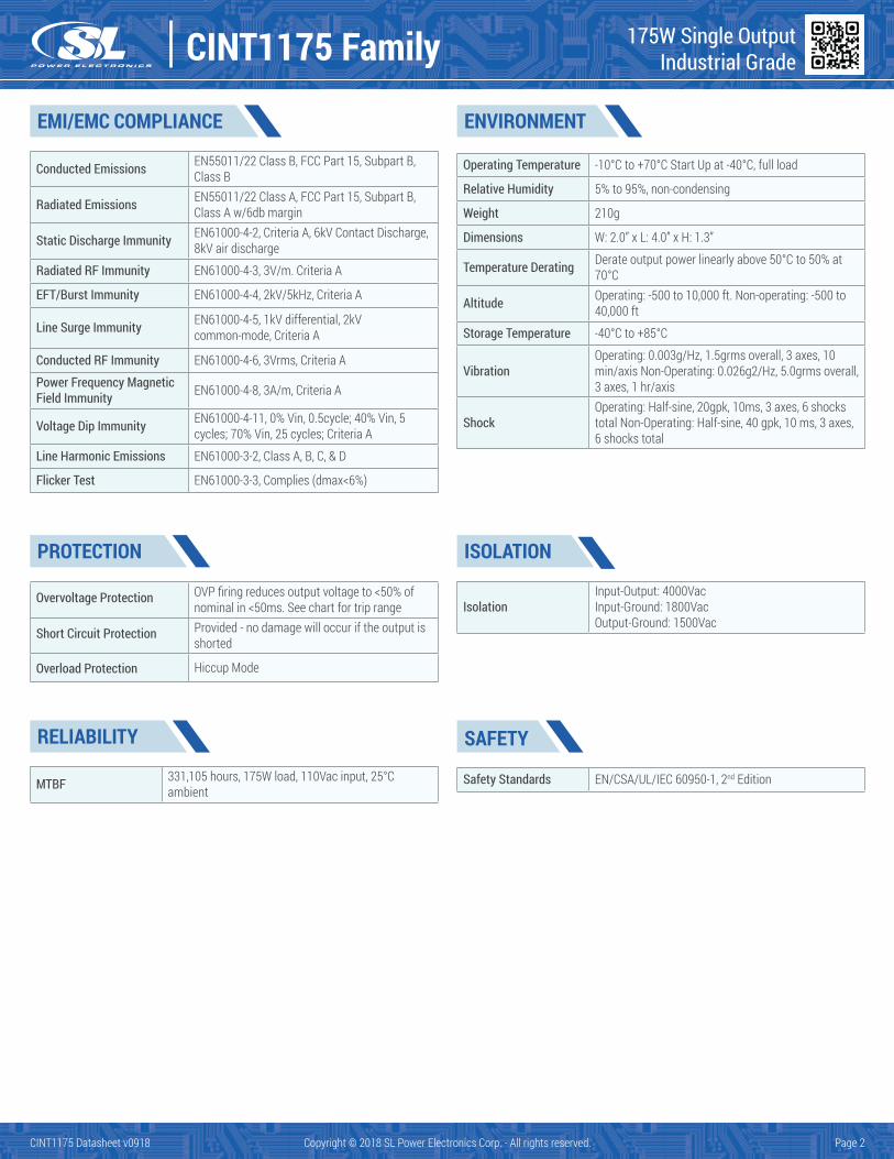
CINT1175 Family 175W Single OutputIndustrial Grade
Page 2CINT1175 Datasheet v0918 Copyright © 2018 SL Power Electronics Corp. - All rights reserved.
Overvoltage Protection OVP firing reduces output voltage to <50% of nominal in <50ms. See chart for trip range
Short Circuit Protection Provided - no damage will occur if the output is shorted
Overload Protection Hiccup Mode
PROTECTION
Conducted Emissions EN55011/22 Class B, FCC Part 15, Subpart B, Class B
Radiated Emissions EN55011/22 Class A, FCC Part 15, Subpart B, Class A w/6db margin
Static Discharge Immunity EN61000-4-2, Criteria A, 6kV Contact Discharge, 8kV air discharge
Radiated RF Immunity EN61000-4-3, 3V/m. Criteria A
EFT/Burst Immunity EN61000-4-4, 2kV/5kHz, Criteria A
Line Surge Immunity EN61000-4-5, 1kV differential, 2kV common-mode, Criteria A
Conducted RF Immunity EN61000-4-6, 3Vrms, Criteria A
Power Frequency Magnetic Field Immunity EN61000-4-8, 3A/m, Criteria A
Voltage Dip Immunity EN61000-4-11, 0% Vin, 0.5cycle; 40% Vin, 5 cycles; 70% Vin, 25 cycles; Criteria A
Line Harmonic Emissions EN61000-3-2, Class A, B, C, & D
Flicker Test EN61000-3-3, Complies (dmax<6%)
EMI/EMC COMPLIANCE
Operating Temperature -10°C to +70°C Start Up at -40°C, full load
Relative Humidity 5% to 95%, non-condensing
Weight 210g
Dimensions W: 2.0” x L: 4.0” x H: 1.3”
Temperature Derating Derate output power linearly above 50°C to 50% at 70°C
Altitude Operating: -500 to 10,000 ft. Non-operating: -500 to 40,000 ft
Storage Temperature -40°C to +85°C
VibrationOperating: 0.003g/Hz, 1.5grms overall, 3 axes, 10 min/axis Non-Operating: 0.026g2/Hz, 5.0grms overall,3 axes, 1 hr/axis
ShockOperating: Half-sine, 20gpk, 10ms, 3 axes, 6 shocks total Non-Operating: Half-sine, 40 gpk, 10 ms, 3 axes, 6 shocks total
ENVIRONMENT
IsolationInput-Output: 4000VacInput-Ground: 1800VacOutput-Ground: 1500Vac
ISOLATION
MTBF 331,105 hours, 175W load, 110Vac input, 25°C ambient
RELIABILITY
Safety Standards EN/CSA/UL/IEC 60950-1, 2nd Edition
SAFETY
CINT1175 Family 175W Single OutputIndustrial Grade
Page 3CINT1175 Datasheet v0918 Copyright © 2018 SL Power Electronics Corp. - All rights reserved.
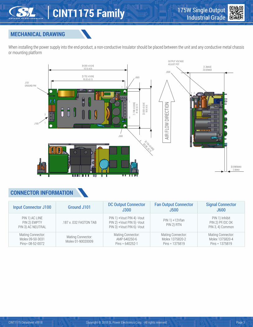
MECHANICAL DRAWING
When installing the power supply into the end-product, a non-conductive Insulator should be placed between the unit and any conductive metal chassisor mounting platform
CONNECTOR INFORMATION
Input Connector J100 Ground J101 DC Output Connector J300
Fan Output Connector J500
Signal ConnectorJ600
PIN 1) AC LINEPIN 2) EMPTY
PIN 3) AC NEUTRAL.187 x .032 FASTON TAB
PIN 1) +Vout PIN 4) -VoutPIN 2) +Vout PIN 5) -VoutPIN 3) +Vout PIN 6) -Vout
PIN 1) +12VfanPIN 2) RTN
PIN 1) InhibitPIN 2) PF/DC OK
PIN 3, 4) Common
Mating Connector:Molex 09-50-3031Pins= 08-52-0072
Mating Connector:Molex 01-90020009
Mating Connector:AMP 640250-6
Pins = 640252-1
Mating Connector:Molex 1375820-2Pins = 1375819
Mating Connector:Molex 1375820-4Pins = 1375819
[4.000 ±0.024]101.6 ±0.6
[1.3MAX]33.02MAX
OUTPUT VOLTAGEADJUST POT
[1.74
8 ±0.0
006]
41.40
±0.15
[2.00
0 ±0.0
24]
50.8
±0.6
AIR
FLOW
DIR
ECTI
ON
J101GROUND PIN
J100
34
41
1
1 2
0
1
[0.156 ±0.006]
Ø3.96 ±0.15
[3.752 ±0.006]95.30 ±0.15
J300
J600
J500
[0.0985MAX2.5MAX
CINT1175 Family 175W Single OutputIndustrial Grade
Page 4CINT1175 Datasheet v0918 Copyright © 2018 SL Power Electronics Corp. - All rights reserved.
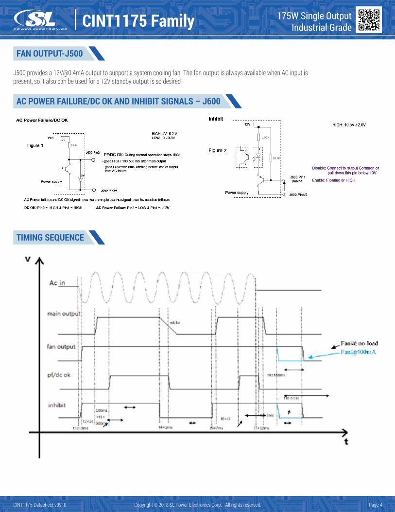
J500 provides a [email protected] output to support a system cooling fan. The fan output is always available when AC input ispresent, so it also can be used for a 12V standby output is so desired
FAN OUTPUT-J500
AC POWER FAILURE/DC OK AND INHIBIT SIGNALS – J600
TIMING SEQUENCE
CINT1175 Family 175W Single OutputIndustrial Grade
Page 5CINT1175 Datasheet v0918 Copyright © 2018 SL Power Electronics Corp. - All rights reserved.
Parameter Conditions/Description Min Nom Max Units
Insulation Safety RatingInput/GroundInput/Output
Output/Ground
BasicReinforced
n/a
Electric Strength Test VoltageInput/GroundInput/Output
Output/Ground
18004,000500
- -VacVacVac
ISOLATION SPECIFICATIONS
Parameter Conditions/Description Min Nom Max Units
Input Voltage 90 115/230 264 VacTurn-On Input Voltage Ramping up 82.7 VacTurn-Off Input Voltage Ramping down 67.0 Vac
Input Frequency 47 50/60 63 HzInrush Current Limitation 264Vac, cold start - - 50 A
Power Factor Vi nom, Io nom 0.9 - -
Efficiency
Vi nom, Io nomCINT1175A1206K01CINT1175A1506K01CINT1175A2406K01CINT1175A4806K01CINT1175A5606K01
- 90% - %
INPUT SPECIFICATIONSAll specifications apply over specified input voltage, output load, and temperature range, unless otherwise noted
CINT1175 Family 175W Single OutputIndustrial Grade
Page 6CINT1175 Datasheet v0918 Copyright © 2018 SL Power Electronics Corp. - All rights reserved.
Parameter Conditions/Description Min Nom Max Units
Output Voltage Setpoint AccuracyCINT1175A1206K01 Vi nom,, Io1 @ ADC, TC = 25 °C -3 - 3 % Vo nom
Output Voltage Setpoint AccuracyCINT1175A1506K01 Vi nom,, Io1 @ ADC, TC = 25 °C -3 - 3 % Vo nom
Output Voltage Setpoint AccuracyCINT1175A2406K01 Vi nom,, Io1 @ ADC, TC = 25 °C -3 - 3 % Vo nom
Output Voltage Setpoint AccuracyCINT1175A4806K01 Vi nom,, Io1 @ ADC, TC = 25 °C -3 - 3 % Vo nom
Output Voltage Setpoint AccuracyCINT1175A5606K01 Vi nom,, Io1 @ ADC, TC = 25 °C -3 - 3 % Vo nom
Output Current V1Output Current V2 CINT1175A1206K01 0
010.0
-14.60.4
ADCADC
Output Current V1Output Current V2 CINT1175A1506K01 0
08.0
-11.70.4
ADCADC
Output Current V1Output Current V2 CINT1175A2406K01 0
05.0
-7.30.4
ADCADC
Output Current V1Output Current V2 CINT1175A4806K01 0
02.5
-3.60.4
ADCADC
Output Current V1Output Current V2 CINT1175A5606K01 0
02.1
-3.10.4
ADCADC
Static Line Regulation V1 Vi min-Vi max, Vi nom, 0-100% lo nom -1 - 1 % Vo nomStatic Load Regulation V1
(Droop Characteristic) Vi min-Vi max, Vi nom, 0-100% lo nom -3 - 3 % Vo nom
Hold-Up Time Starting at Vi = 230 VAC, Po nom - 16 - ms
Dynamic Load Regulation Load change =50%, di/dt =0.2A/μSvoltage deviation 3% 0 2 % Vo nom
Start-Up Time Vi nom,lo nom 0 - 3 s
OUTPUT SPECIFICATIONS
PROTECTION
Parameter Conditions/Description Min Nom Max Units
Input Fuse Not user accessibleInput Transient Protection 2KV(CM) and 1KV(DM) surge 2
OutputNo-load and short circuit proof Hiccup or Latch
short circuit proof Hiccup or Latchoverload (latch style) Hiccup
Overvoltage Protection Latch style LatchOver temperature Protection Automatic power shutdown at TC =155°C
All specifications apply over specified input voltage, output load, and temperature range, unless otherwise noted
CINT1175 Family 175W Single OutputIndustrial Grade
Page 7CINT1175 Datasheet v0918 Copyright © 2018 SL Power Electronics Corp. - All rights reserved.
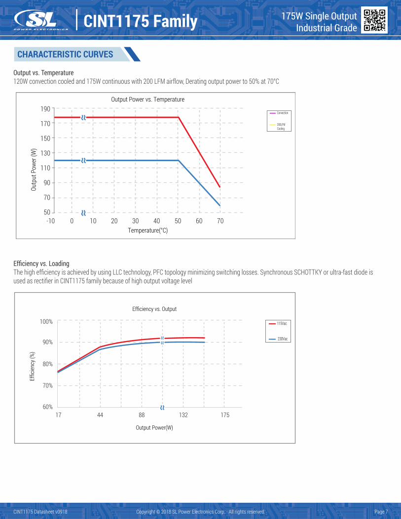
CHARACTERISTIC CURVES
50
70
90
110
130
150
170
190
-10 0 10 20 30 40 50 60 70
Outp
ut P
ower
(W)
Temperature(°C)
Output Power vs. Temperature
Convection
200LFM Cooling
Efficiency vs. LoadingThe high efficiency is achieved by using LLC technology, PFC topology minimizing switching losses. Synchronous SCHOTTKY or ultra-fast diode isused as rectifier in CINT1175 family because of high output voltage level
Output vs. Temperature120W convection cooled and 175W continuous with 200 LFM airflow, Derating output power to 50% at 70°C
17 44 88 132 175
Effic
iency
(%)
Efficiency vs. Output
Output Power(W)
115Vac
230Vac
100%
90%
80%
70%
60%
CINT1175 Family 175W Single OutputIndustrial Grade
Page 8CINT1175 Datasheet v0918 Copyright © 2018 SL Power Electronics Corp. - All rights reserved.
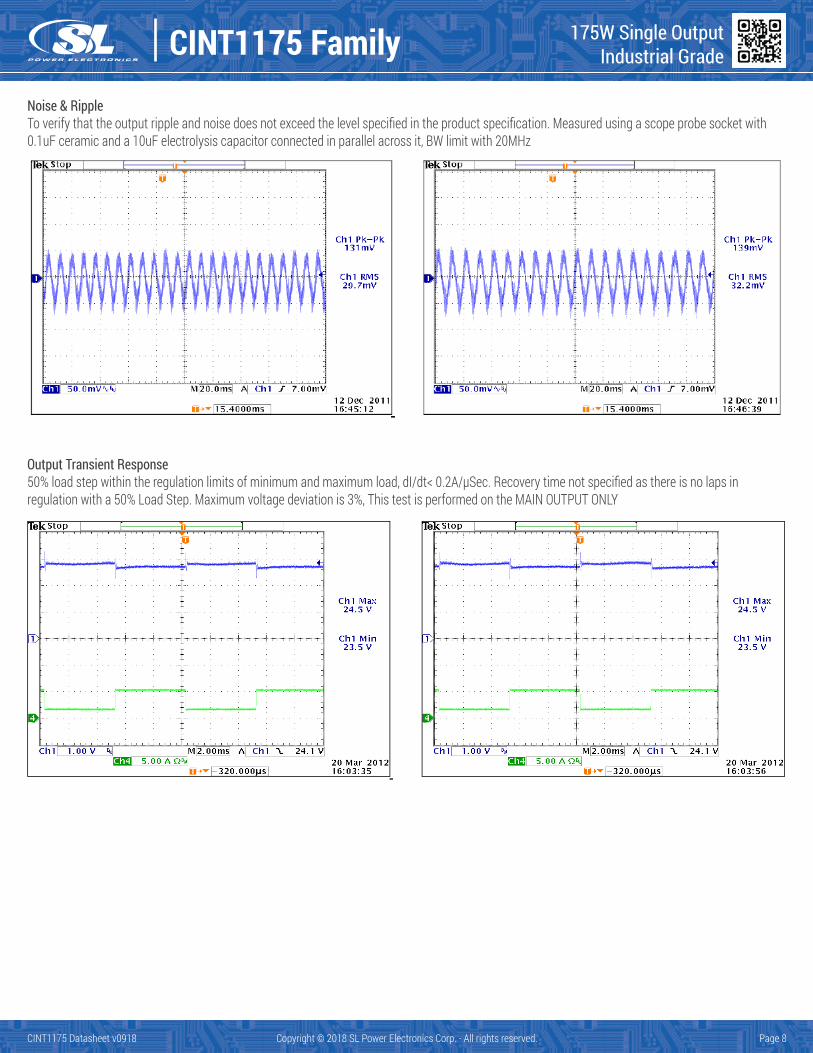
Noise & RippleTo verify that the output ripple and noise does not exceed the level specified in the product specification. Measured using a scope probe socket with0.1uF ceramic and a 10uF electrolysis capacitor connected in parallel across it, BW limit with 20MHz
Output Transient Response50% load step within the regulation limits of minimum and maximum load, dI/dt< 0.2A/μSec. Recovery time not specified as there is no laps in regulation with a 50% Load Step. Maximum voltage deviation is 3%, This test is performed on the MAIN OUTPUT ONLY
CINT1175 Family 175W Single OutputIndustrial Grade
Page 9CINT1175 Datasheet v0918 Copyright © 2018 SL Power Electronics Corp. - All rights reserved.
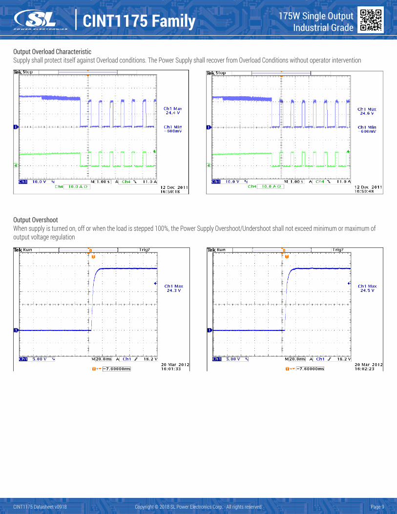
Output Overload CharacteristicSupply shall protect itself against Overload conditions. The Power Supply shall recover from Overload Conditions without operator intervention
Output OvershootWhen supply is turned on, off or when the load is stepped 100%, the Power Supply Overshoot/Undershoot shall not exceed minimum or maximum ofoutput voltage regulation