Characterization of afm surface modification on lbmo
15
Characterization of surface modification in atomic force microscope-induced nanolithography of oxygen deficient La0.67Ba0.33MnO3−δ thin films E. Kevin Tanyi, Rajeswari M. Kolagani, Parul Srivastava, William Vanderlinde, Grace Yong, Christopher Stumpf, and David Schaefer Citation: AIP Advances 4, 127129 (2014); doi: 10.1063/1.4904427 View online: http://dx.doi.org/10.1063/1.4904427 View Table of Contents: http://scitation.aip.org/content/aip/journal/adva/4/12?ver=pdfcov Published by the AIP Publishing Articles you may be interested in Continuously-tuned tunneling behaviors of ferroelectric tunnel junctions based on BaTiO3/La0.67Sr0.33MnO3 heterostructure AIP Advances 4, 057106 (2014); 10.1063/1.4876234 Strain induced tunable anisotropic magnetoresistance in La0.67Ca0.33MnO3/BaTiO3 heterostructures J. Appl. Phys. 113, 17C716 (2013); 10.1063/1.4795841 Characterization of surface and interface structure of Y Ba 2 Cu 3 O 7 − δ -based trilayer with La 0.67 Ca 0.33 Mn O 3 spacer J. Appl. Phys. 99, 08M509 (2006); 10.1063/1.2176319 Magnetic and transport properties of Mo substituted La 0.67 Ba 0.33 Mn 1 − x Mo x O 3 perovskite system J. Appl. Phys. 98, 013905 (2005); 10.1063/1.1947897 Oxidation kinetics in La 0.67 Ba 0.33 MnO 3−δ epitaxy on SrTiO 3 (001) during pulsed-laser deposition Appl. Phys. Lett. 74, 3540 (1999); 10.1063/1.124154 All article content, except where otherwise noted, is licensed under a Creative Commons Attribution 3.0 Unported license. See: http://creativecommons.org/licenses/by/3.0/ Downloaded to IP: 98.204.219.24 On: Tue, 16 Dec 2014 21:36:21
-
Upload
christopher-stumpf -
Category
Science
-
view
53 -
download
1
Transcript of Characterization of afm surface modification on lbmo

Characterization of surface modification in atomic force microscope-inducednanolithography of oxygen deficient La0.67Ba0.33MnO3−δ thin filmsE. Kevin Tanyi, Rajeswari M. Kolagani, Parul Srivastava, William Vanderlinde, Grace Yong, ChristopherStumpf, and David Schaefer Citation: AIP Advances 4, 127129 (2014); doi: 10.1063/1.4904427 View online: http://dx.doi.org/10.1063/1.4904427 View Table of Contents: http://scitation.aip.org/content/aip/journal/adva/4/12?ver=pdfcov Published by the AIP Publishing Articles you may be interested in Continuously-tuned tunneling behaviors of ferroelectric tunnel junctions based on BaTiO3/La0.67Sr0.33MnO3heterostructure AIP Advances 4, 057106 (2014); 10.1063/1.4876234 Strain induced tunable anisotropic magnetoresistance in La0.67Ca0.33MnO3/BaTiO3 heterostructures J. Appl. Phys. 113, 17C716 (2013); 10.1063/1.4795841 Characterization of surface and interface structure of Y Ba 2 Cu 3 O 7 − δ -based trilayer with La 0.67 Ca0.33 Mn O 3 spacer J. Appl. Phys. 99, 08M509 (2006); 10.1063/1.2176319 Magnetic and transport properties of Mo substituted La 0.67 Ba 0.33 Mn 1 − x Mo x O 3 perovskite system J. Appl. Phys. 98, 013905 (2005); 10.1063/1.1947897 Oxidation kinetics in La 0.67 Ba 0.33 MnO 3−δ epitaxy on SrTiO 3 (001) during pulsed-laser deposition Appl. Phys. Lett. 74, 3540 (1999); 10.1063/1.124154
All article content, except where otherwise noted, is licensed under a Creative Commons Attribution 3.0 Unported license. See:
http://creativecommons.org/licenses/by/3.0/ Downloaded to IP: 98.204.219.24 On: Tue, 16 Dec 2014 21:36:21

AIP ADVANCES 4, 127129 (2014)
Characterization of surface modification in atomic forcemicroscope-induced nanolithography of oxygen deficientLa0.67Ba0.33MnO3−δ thin films
E. Kevin Tanyi,1,a Rajeswari M. Kolagani,1,b Parul Srivastava,1William Vanderlinde,2 Grace Yong,1 Christopher Stumpf,1and David Schaefer11Department of Physics, Astronomy & Geosciences, Towson University, Towson MD 21043,U.S.A2Laboratory for Physical Sciences, 8050 Greenmead Drive, College Park, MD 20740, U.S.A
(Received 2 June 2014; accepted 27 November 2014; published online 16 December 2014)
We report our studies of the nanolithographic surface modifications induced by anAtomic Force Microscope (AFM) in epitaxial thin films of oxygen deficient Lan-thanum Barium Manganese Oxide (La0.67Ba0.33MnO3−δ). The pattern characteristicsdepend on the tip voltage, tip polarity, voltage duration, tip force, and humidity.We have used Electron Energy Dispersive X-Ray Spectroscopy (EDS) to analyzethe chemical changes associated with the surface modifications produced with anegatively biased AFM tip. A significant increase in the oxygen stoichiometry forthe patterned regions relative to the pristine film surface is observed. The results alsoindicate changes in the cation stoichiometry, specifically a decrease in the Lanthanumand Manganese concentrations and an increase in the Barium concentration in thepatterned regions. C 2014 Author(s). All article content, except where otherwisenoted, is licensed under a Creative Commons Attribution 3.0 Unported License.[http://dx.doi.org/10.1063/1.4904427]
I. INTRODUCTION
Nanolithographic surface modification via anodic oxidation has attracted significant interestsince 1990, when Dagata et al1 demonstrated localized oxidation of passivated Silicon (Si) samplesusing a scanning tunneling microscope (STM). Similar phenomena were also demonstrated usingthe Atomic Force Microscope (AFM). It has been found that the pattern characteristics such asthe height and width are dependent on several parameters such as the electric field (voltage andtip-to-sample distance), humidity, voltage pulse duration, tip speed, and the mode of the AFMoperation – i.e. contact mode or tapping mode.2–10 Several models including those by Gordon etal,11 Teuschler et al12 and the Cabrera and Mott13 have been proposed to explain the experimentalresults. In the case of metals such as Ti and Al14–16 and semiconductors such as Si2,5 a detailedunderstanding of the chemical processes associated with STM/AFM-induced nanolithography hasbeen established. AFM induced nanolithographic modification of functional complex metal oxideshas attracted some attention in recent years as evidenced by studies on SrTiO3
17, high tempera-ture superconducting materials such YBa2Cu3O7
18–20 and HoBa2Cu3O7−x21 as well as thin films
of rare earth manganese oxides exhibiting colossal magnetoresistance and charge ordering.22–30
However, unlike in the case of Si and simple metallic systems, there have been no previous ef-forts to understand the nature of the chemical modifications in the metal oxide materials. Earlierwork by Run Wei et al22,23 has demonstrated AFM lithography in thin films of La0.8Ba0.2MnO3,focusing on features introduced by positive tip bias (‘negative sample voltage’ in their terminology)in fully oxygenated samples. Their studies mainly address the morphological characteristics of
aCurrently at Norfolk State [email protected] (To whom all correspondence should be addressed)
2158-3226/2014/4(12)/127129/14 4, 127129-1 ©Author(s) 2014
All article content, except where otherwise noted, is licensed under a Creative Commons Attribution 3.0 Unported license. See:
http://creativecommons.org/licenses/by/3.0/ Downloaded to IP: 98.204.219.24 On: Tue, 16 Dec 2014 21:36:21

127129-2 Tanyi et al. AIP Advances 4, 127129 (2014)
the pattern and etch selectivity resulting from the surface modification. Pallechi et alhave em-ployed surface modification induced by an AFM tip to pattern device structures in LBMO films,employing the increase in resistance to obtain resistive barriers.25–27 These researchers have demon-strated patterning using negative tip bias in films with different oxygen content, but their focushas been on subsequent field effect studies in the patterned devices by application of external elec-tric field. Yanagisawa et al28,29 have used AFM lithography to pattern thin films phase separatedLa0.275Pr0.35CaMnO3 thin films. They have reported that larger pattern heights can be obtained foroxygen deficient films as compared to oxygen-annealed samples for positive tip bias. The emphasisof their work however, was on changes in the insulator-metal transition temperature and electricaland magneto-resistive properties induced by the surface modification.
In this paper, we report our studies of the AFM-induced nanolithography in an oxygen defi-cient composition of the colossal magneto-resistive material Lanthanum Barium Manganese oxide(La0.67Ba0.33MnO3−δ), abbreviated as LBMO). In the fully oxygenated state (La0.67Ba0.33MnO3),this material undergoes an insulator-to-metal transition accompanied by ferromagnetic orderingabove room temperature and shows colossal magneto-resistance24 which makes it important forpotential spintronic devices. For the present study, the LBMO thin films are intentionally fabricatedso as to be oxygen deficient since oxygen deficiency may be expected to enhance the effects ofanodic oxidation. Oxygen deficient films also have reduced surface roughness which is advanta-geous for AFM lithography. The study reported here focuses on surface modifications induced bya negatively biased AFM tip which produces large outgrowths. We have analyzed the chemicalchanges associated with these outgrowths using Electron Energy Dispersive x-ray spectroscopy(EDS).
II. EXPERIMENTAL DETAILS
A. Sample preparation and characterization
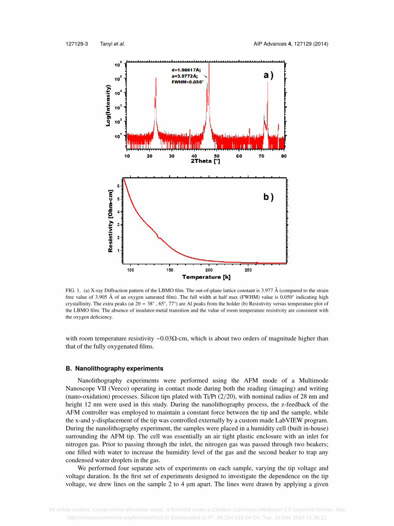
The LBMO films were grown on SrTiO3 (100) (abbreviated as STO) by Pulsed Laser Deposi-tion using a Krypton Fluoride (KrF) laser of wavelength 248 nm and pulse width 20 ns, operated at10 Hz. The substrate temperature during film growth was 800C, with laser pulse energy of 450 mJcorresponding to an energy density ∼ 1 J/cm2 on the target. During film growth an ambient offlowing oxygen was maintained at a partial pressure of 50 mTorr (66.5 µbar) [Note that the ox-ygen pressure needed for the optimally oxygenated phase is 400 mTorr under our experimentalconditions. The oxygen pressure was reduced to achieve oxygen deficient composition in the filmsfor the present study]. The films were cooled down to room temperature in oxygen ambient of ∼500 Torr at a nominal cooling rate of 20 C/min. The average film thickness was 1,400 Å, thegrowth rate being 0.14 Å/pulse. The structural properties of the films were characterized using afour circle X-ray diffractometer (Bruker D8 Discover). The results reveal (00l) oriented films withgood crystalline quality as indicated by a rocking angle (FWHM) of 0.05. The 2θ − ω scan of atypical sample is shown in Fig.1 (a). Φ scans (not shown) reveal that the films are in-plane-alignedwith a cube-on-cube epitaxial alignment with the substrate. The out of plane lattice constant isdetermined to be 3.97 Å (in the pseudo-cubic notation). Note that this value of the lattice constant issignificantly larger than the c-lattice constant of the fully oxygenated bulk phase, which is 3.90 Å.The expanded c-lattice constant is indicative of the oxygen deficient phase, the expansion resultingfrom the lattice distortion and the increased Mn3+ ion fraction compared to the fully oxygenatedphase. Prior to patterning, we characterized the surface morphology of the films using atomic forcemicroscopy. The average roughness (Ra) value obtained for all the samples used was 0.18 nmwith a standard deviation of 0.01 nm. It is noteworthy to mention that these films are significantlysmoother that the fully oxygenated samples which typically have an order of magnitude higheraverage surface roughness. This can be understood as resulting from the higher kinetic energy ofthe adatoms due to the increased mean free path between collisions facilitated by the lower oxygenpressure. Fig.1 (b) shows a representative resistivity versus temperature for the samples in thisstudy. The samples are insulating at room temperature as expected for oxygen deficient samples
All article content, except where otherwise noted, is licensed under a Creative Commons Attribution 3.0 Unported license. See:
http://creativecommons.org/licenses/by/3.0/ Downloaded to IP: 98.204.219.24 On: Tue, 16 Dec 2014 21:36:21
127129-3 Tanyi et al. AIP Advances 4, 127129 (2014)
FIG. 1. (a) X-ray Diffraction pattern of the LBMO film. The out-of-plane lattice constant is 3.977 Å (compared to the strainfree value of 3.905 Å of an oxygen saturated film). The full width at half max (FWHM) value is 0.050 indicating highcrystallinity. The extra peaks (at 2θ = 38 , 65, 77) are Al peaks from the holder (b) Resistivity versus temperature plot ofthe LBMO film. The absence of insulator-metal transition and the value of room temperature resistivity are consistent withthe oxygen deficiency.
with room temperature resistivity ∼0.03Ω-cm, which is about two orders of magnitude higher thanthat of the fully oxygenated films.
B. Nanolithography experiments
Nanolithography experiments were performed using the AFM mode of a MultimodeNanoscope VII (Veeco) operating in contact mode during both the reading (imaging) and writing(nano-oxidation) processes. Silicon tips plated with Ti/Pt (2/20), with nominal radius of 28 nm andheight 12 nm were used in this study. During the nanolithography process, the z-feedback of theAFM controller was employed to maintain a constant force between the tip and the sample, whilethe x-and y-displacement of the tip was controlled externally by a custom made LabVIEW program.During the nanolithography experiment, the samples were placed in a humidity cell (built in-house)surrounding the AFM tip. The cell was essentially an air tight plastic enclosure with an inlet fornitrogen gas. Prior to passing through the inlet, the nitrogen gas was passed through two beakers;one filled with water to increase the humidity level of the gas and the second beaker to trap anycondensed water droplets in the gas.
We performed four separate sets of experiments on each sample, varying the tip voltage andvoltage duration. In the first set of experiments designed to investigate the dependence on the tipvoltage, we drew lines on the sample 2 to 4 µm apart. The lines were drawn by applying a given
All article content, except where otherwise noted, is licensed under a Creative Commons Attribution 3.0 Unported license. See:
http://creativecommons.org/licenses/by/3.0/ Downloaded to IP: 98.204.219.24 On: Tue, 16 Dec 2014 21:36:21

127129-4 Tanyi et al. AIP Advances 4, 127129 (2014)
voltage across the tip while moving the tip across the surface in a linear path. As the voltage biasedtip is moved across the surface it modifies the surface creating outgrowths that form a line. Thevoltage bias was then removed and the tip was moved back down to its initial starting position. Anoffset voltage was then applied to move the tip to a new position on the surface 2 to 4µm away andthe process was repeated to draw the next line. The lines so drawn were 16 µm long. For each linedrawn, we recorded the temperature and humidity near the sample surface. The results reported herewere obtained at an average relative humidity of ∼75%. The lowest humidity needed to obtain anysurface modification was 61% and the maximum attainable relative humidity was 85%.
During a second set of experiments, while holding the tip at a fixed position above the sample,we applied voltage pulses of varying magnitude and sign for varying time durations, details ofwhich are discussed in the next section. We then moved the tip to a new spot 2-4 µm away andrepeated the process, successively increasing the duration of the voltage pulse. This process created‘dots’ whose height and width characteristics were dependent on the time duration, with all theother parameters held constant. From the height and width data thus obtained, a growth rate wasestablished.
C. Chemical analysis using energy dispersive x-ray spectroscopy (EDS)
Chemical analysis of the sample surface was performed in a LEO 1550 FE scanning electronmicroscope equipped with a Thermo Scientific NORAN System 7 X-ray microanalysis system witha 60 mm2 area silicon drift detector (SDD). In EDS, the sample is bombarded with electrons toknock out core electrons thus stimulating the emission of characteristic X-rays from the specimen.The limitations of EDS for thin film analysis must be kept in mind as the X-rays typically originatefrom a depth of up to a micron in the sample, resulting in limited spatial resolution. Hence for thinfilms, care must be taken to avoid measuring x-rays from the underlying substrate. This limitationis particularly serious when analyzing oxygen stoichiometry in metal oxide thin films when thesubstrates are also oxides. It can also affect the analysis of cation stoichiometry when the film andthe substrate contain same cations. The attenuation depth for the electron beam depends on theelectron energy, the material being analyzed, and the tilt of the sample, and can be modelled usingMonte Carlo simulation methods. Such simulations have shown that it is possible to get reliableresults from thin film layers 100 nm or less in thickness by using low electron beam energy of5 keV.31 We have performed simulations for LBMO thin films on SrTiO3 to identify suitableenergies for our film thickness. The details are discussed in the following section.
III. RESULTS AND DISCUSSION
A. Voltage polarity and magnitude dependence of nanolithography characteristics
With a positive tip bias relative to the sample, we were consistently able to draw well definedand reproducible line patterns, the threshold voltage for line formation being 5V.. In Fig. 2 (a) andFig. 2 (b) we show lines drawn with positive tip voltage in the range 1 V to 10 V and 11 V to 20 Vrespectively, using write speeds of 1.6 µm/s. The widths of these structures were generally between0.3 µm to 1.5 µm. We were able to control the widths by choosing a moderate voltage below 10 Vand adjusting the writing speed, indicating the potential for fabrication of sub-micron features inLBMO films using AFM lithography.
Interestingly, reversing the voltage polarity, (i.e. with tip negatively biased with respect to thesample) produced remarkably different results for the same write speed of 1.6µm/s. The thresholdvoltage for line formation in this case is generally found to be between -9 V and -11V, with the-9V threshold occurring most frequently. In Fig. 3 (a) we show the pattern observed while varyingthe voltage from -11 V to -20 V with a write speed set at 1.6 µm/s. We found that at these highervoltages, excessive outgrowths occur, which prevent the tip from moving, resulting in the formationof a large laterally extending feature instead of well separated lines. However, by increasing thewrite speed to 16 µm/s and the line spacing from 2 µm to 4 µm, we were capable of writingcontrollable and reproducible lines with voltages ∼-15 V, as shown in Fig.3 (b).
All article content, except where otherwise noted, is licensed under a Creative Commons Attribution 3.0 Unported license. See:
http://creativecommons.org/licenses/by/3.0/ Downloaded to IP: 98.204.219.24 On: Tue, 16 Dec 2014 21:36:21

127129-5 Tanyi et al. AIP Advances 4, 127129 (2014)
FIG. 2. (a) Lines created using a tip voltage of +1 V to +10 V at a write speed of 1.6 µm/s (b) Lines created using a tipvoltage of +11 V to +20 V at a write speed of 1.6 µm/s.
The voltage polarity dependence we observe in the oxygen deficient (La0.7Ba0.3MnO3−δ) filmsis qualitatively similar to that observed by Liu et alin post-annealed La0.8Ba0.2MnO3 films,23 thenegative tip bias resulting in more pronounced surface modification. This may be understood asrelated to the fact that negative tip bias (equivalent to positive sample bias as denoted by Liu et al)drive OH−1 ions to the sample surface resulting in anodic oxidation which may result in outgrowths.However, it is noteworthy that writing is possible even with the opposite polarity, which suggeststhat there are other electrochemical processes at work in addition to anodic oxidation. Such pro-cesses involving cation stoichiometry changes are borne out in our EDS analysis presented in thenext section.
We have investigated the dependence of the line height on the magnitude of the tip bias voltagefor both voltage polarities. As shown in Fig.4, line height increases with positive tip voltage. Aslight plateau is observed between 10 V and 12 V. It is possible that the plateau region may beseparating the two different voltage regimes distinguished by different physical/chemical processesinvolved in the formation of the pattern. When the same experiment was repeated with a negativetip voltage, we obtained a similar dependence of the line height on the tip voltage (as is alsoshown in Fig.4). However, the line height obtained with a negative bias was generally higher thanthat obtained with a positive tip bias of the same magnitude. This suggests a polarity dependentdifference in the surface modification indicative of electrolytic processes. As in the case of lines,
All article content, except where otherwise noted, is licensed under a Creative Commons Attribution 3.0 Unported license. See:
http://creativecommons.org/licenses/by/3.0/ Downloaded to IP: 98.204.219.24 On: Tue, 16 Dec 2014 21:36:21

127129-6 Tanyi et al. AIP Advances 4, 127129 (2014)
FIG. 3. (a) Uncontrolled growth pattern observed using a tip voltage of -20 V to -11 V at a write speed of 1.6 µm/s.(Temperature=85.6F and relative humidity = 72%) (b) Lines created using a tip voltage of -15 V to -6 V at a write speed of16.0 µm/s. (Temperature= 88.2 F and relative humidity = 66 %). The voltage threshold for this particular area of the filmwas around -11 V.
FIG. 4. Line heights created by varying the bias polarities and voltages. The negative voltages clearly show much largerfeatures than those generated by the positive voltages.
All article content, except where otherwise noted, is licensed under a Creative Commons Attribution 3.0 Unported license. See:
http://creativecommons.org/licenses/by/3.0/ Downloaded to IP: 98.204.219.24 On: Tue, 16 Dec 2014 21:36:21

127129-7 Tanyi et al. AIP Advances 4, 127129 (2014)
FIG. 5. (a) Comparison of the height of the dots produced at 10 V for various durations of a voltage pulse. Once again, thenegative voltage biases produce the highest features (b) Variation of the width of the dots produced at -10 V with the durationof the pulse. The widths saturate after a duration of ∼ 5 seconds.
we found a large difference between the heights of ‘dots’ created with a positive tip voltage of10V from those created with a negative tip voltage of -10 V, the latter being an order of magnitudelarger for the same duration of the voltage pulse, as shown in Fig.5(a). The negative tip voltagepulse once again created higher features. Fig.5(b) shows a plot of the width of the dots producedwith a negative tip voltage versus the voltage pulse duration for a -10 V voltage pulse. The width
FIG. 6. This is a matrix of dots drawn by varying the duration of the -10 V pulse from 1 s (left- most column) to 10 s(right-most column).
All article content, except where otherwise noted, is licensed under a Creative Commons Attribution 3.0 Unported license. See:
http://creativecommons.org/licenses/by/3.0/ Downloaded to IP: 98.204.219.24 On: Tue, 16 Dec 2014 21:36:21
127129-8 Tanyi et al. AIP Advances 4, 127129 (2014)
initially increases linearly with time and saturates after ∼ 5 seconds. A matrix of dots patterned bythis process is shown in Fig.6, with widths in the range 1.2 µm to 1.4 µm. We were able to getsub-micron dots with negative tip voltage pulses with pulse duration of about 0.001 to 0.1 seconds,indicating potential for a fast writing process.
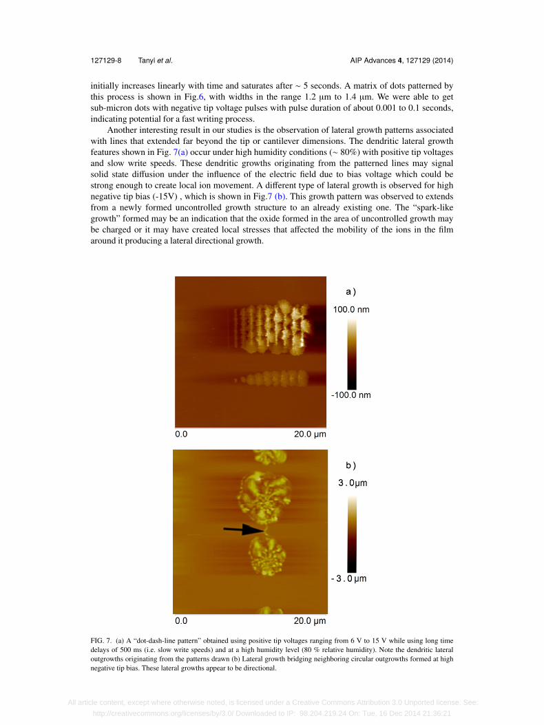
Another interesting result in our studies is the observation of lateral growth patterns associatedwith lines that extended far beyond the tip or cantilever dimensions. The dendritic lateral growthfeatures shown in Fig. 7(a) occur under high humidity conditions (∼ 80%) with positive tip voltagesand slow write speeds. These dendritic growths originating from the patterned lines may signalsolid state diffusion under the influence of the electric field due to bias voltage which could bestrong enough to create local ion movement. A different type of lateral growth is observed for highnegative tip bias (-15V) , which is shown in Fig.7 (b). This growth pattern was observed to extendsfrom a newly formed uncontrolled growth structure to an already existing one. The “spark-likegrowth” formed may be an indication that the oxide formed in the area of uncontrolled growth maybe charged or it may have created local stresses that affected the mobility of the ions in the filmaround it producing a lateral directional growth.
FIG. 7. (a) A “dot-dash-line pattern” obtained using positive tip voltages ranging from 6 V to 15 V while using long timedelays of 500 ms (i.e. slow write speeds) and at a high humidity level (80 % relative humidity). Note the dendritic lateraloutgrowths originating from the patterns drawn (b) Lateral growth bridging neighboring circular outgrowths formed at highnegative tip bias. These lateral growths appear to be directional.
All article content, except where otherwise noted, is licensed under a Creative Commons Attribution 3.0 Unported license. See:
http://creativecommons.org/licenses/by/3.0/ Downloaded to IP: 98.204.219.24 On: Tue, 16 Dec 2014 21:36:21

127129-9 Tanyi et al. AIP Advances 4, 127129 (2014)
B. SEM/EDS analysis
We have employed elemental analysis using Energy Dispersive X-ray Spectroscopy (EDS)to investigate chemical changes associated with the large outgrowths produced by the negativelybiased AFM tip. Images of the patterned lines were also recorded using the scanning electronmicroscope (SEM). SEM images of lines that were produced using a negative tip bias at varyingline speeds are shown in Fig.8(a). The trench visible in the middle of each line is as a result ofabrasion, as the oxide grows higher than the z-feedback limit of the AFM. This image clearly showsthat the pattern produced does affect regions further away from the tip, indicating that the materialused to form the growth pattern is pulled from neighboring regions. Fig.8(b) shows a larger areathat was patterned using negative tip bias, which produces lines at low voltages and the uncontrol-lable outgrowths at higher voltages, as mentioned earlier. This SEM image also includes some dotpatterns. The dot patterns were produced with voltages greater than -15 V, which cause the dots togrow very fast. The smallest dot was produced with a voltage pulse of about 10 s. The SEM imagein Fig. 8(c) is a magnified version of the edge of one of the large dots in Fig. 8(b), showing cracks
FIG. 8. (a) SEM image of the line patterns produced with a negatively biased voltage at varying line speeds. The trenchvisible in the middle of each line is as a result of abrasion as the oxide grows higher than the z-feedback limit (b) Dot patternsproduced with voltages greater than -15V (c) Magnified version of the edge of one of the large dots shown in figure 8(b),indicating cracks within the oxide that forms the pattern.
All article content, except where otherwise noted, is licensed under a Creative Commons Attribution 3.0 Unported license. See:
http://creativecommons.org/licenses/by/3.0/ Downloaded to IP: 98.204.219.24 On: Tue, 16 Dec 2014 21:36:21
127129-10 Tanyi et al. AIP Advances 4, 127129 (2014)
within the material that forms the pattern. We believe that these cracks may be the result of stressesdue to localized changes in the crystal structure accompanying oxidation or cationic diffusion. Thehuge extent of the lateral growth of the patterns formed with negative voltages greater than -15 Vmay be associated with the trapping of moisture in these cracks, which promotes the propagationof the oxidation reaction. In other words, the oxide formed using a negatively biased tip is notself-limiting.
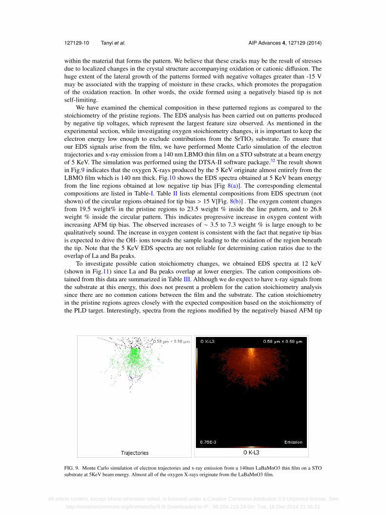
We have examined the chemical composition in these patterned regions as compared to thestoichiometry of the pristine regions. The EDS analysis has been carried out on patterns producedby negative tip voltages, which represent the largest feature size observed. As mentioned in theexperimental section, while investigating oxygen stoichiometry changes, it is important to keep theelectron energy low enough to exclude contributions from the SrTIO3 substrate. To ensure thatour EDS signals arise from the film, we have performed Monte Carlo simulation of the electrontrajectories and x-ray emission from a 140 nm LBMO thin film on a STO substrate at a beam energyof 5 KeV. The simulation was performed using the DTSA-II software package.32 The result shownin Fig.9 indicates that the oxygen X-rays produced by the 5 KeV originate almost entirely from theLBMO film which is 140 nm thick. Fig.10 shows the EDS spectra obtained at 5 KeV beam energyfrom the line regions obtained at low negative tip bias [Fig 8(a)]. The corresponding elementalcompositions are listed in Table-I. Table II lists elemental compositions from EDS spectrum (notshown) of the circular regions obtained for tip bias > 15 V[Fig. 8(b)] . The oxygen content changesfrom 19.5 weight% in the pristine regions to 23.5 weight % inside the line pattern, and to 26.8weight % inside the circular pattern. This indicates progressive increase in oxygen content withincreasing AFM tip bias. The observed increases of ∼ 3.5 to 7.3 weight % is large enough to bequalitatively sound. The increase in oxygen content is consistent with the fact that negative tip biasis expected to drive the OH- ions towards the sample leading to the oxidation of the region beneaththe tip. Note that the 5 KeV EDS spectra are not reliable for determining cation ratios due to theoverlap of La and Ba peaks.
To investigate possible cation stoichiometry changes, we obtained EDS spectra at 12 keV(shown in Fig.11) since La and Ba peaks overlap at lower energies. The cation compositions ob-tained from this data are summarized in Table III. Although we do expect to have x-ray signals fromthe substrate at this energy, this does not present a problem for the cation stoichiometry analysissince there are no common cations between the film and the substrate. The cation stoichiometryin the pristine regions agrees closely with the expected composition based on the stoichiometry ofthe PLD target. Interestingly, spectra from the regions modified by the negatively biased AFM tip
FIG. 9. Monte Carlo simulation of electron trajectories and x-ray emission from a 140nm LaBaMnO3 thin film on a STOsubstrate at 5KeV beam energy. Almost all of the oxygen X-rays originate from the LaBaMnO3 film.
All article content, except where otherwise noted, is licensed under a Creative Commons Attribution 3.0 Unported license. See:
http://creativecommons.org/licenses/by/3.0/ Downloaded to IP: 98.204.219.24 On: Tue, 16 Dec 2014 21:36:21

127129-11 Tanyi et al. AIP Advances 4, 127129 (2014)
FIG. 10. Energy Dispersive X-ray Spectra (EDS) of LBMO obtained with a 5 keV electron beam. (a) EDS Spectrum from apristine unmodified region of the sample (b) EDS Spectrum from a sample modified by AFM lithography with a negativelybiased tip.
TABLE I. Comparison of the oxygen stoichiometry of a pristine region in the sample to the oxygen stoichiometry in theregion modified by a negative tip voltage using EDS data obtained with an electron beam energy of 5 KeV. The area analyzedis one of the lines shown in Fig.8(a). Note that the cation composition cannot be resolved at 5 KeV.
Element–X-ray Line
Weight % :Pristine Region
Weight % :Modified Region
Change in weight %:Modified Region % Change
C-K 3.1 4.9 1.8 58.1O-K 19.5 23.0 3.5 17.9Mn-L 46.6 47.3 0.70 1.5La-L 30.9 24.8 -6.1 -19.7
All article content, except where otherwise noted, is licensed under a Creative Commons Attribution 3.0 Unported license. See:
http://creativecommons.org/licenses/by/3.0/ Downloaded to IP: 98.204.219.24 On: Tue, 16 Dec 2014 21:36:21

127129-12 Tanyi et al. AIP Advances 4, 127129 (2014)
TABLE II. Comparison of the oxygen stoichiometry of a pristine region in the sample to the oxygen stoichiometry in theregion modified by a negative tip voltage using EDS data obtained with an electron beam energy of 5 KeV. The area analyzedis one of the dots shown in Fig.8(b). Note that the cation composition cannot be resolved at 5 KeV.
Element–X-ray Line
Weight % :Pristine Region
Weight % :Modified Region
Change in weight %:Modified Region % Change
C-K 3.1 6.5 3.4 109.4O-K 19.5 26.8 7.3 37.6Mn-K 46.6 41.4 -5.2 -11.2La-L 30.9 25.3 -5.6 -18.2
reveal changes in the La to Ba ratio, corresponding to a Ba rich composition in these regions. Thissuggests ionic diffusion during the patterning process under the influence of electric field gradients,consistent with the lateral outgrowths described earlier. Also, we observe a reduction of Mn contentin the patterned areas.
It is also important to note that the substrate composition is also affected as shown by thedrop in the Ti and Sr concentrations. These results were consistent with some etching experimentswe have carried out indicating that chemical modifications extend into the surface layers of thesubstrate. In order to understand the chemical mechanisms behind the observed changes calls forfurther experiments which we are currently working on.
FIG. 11. Energy Dispersive X-ray Spectra (EDS) of LBMO obtained with a 12 keV electron beam. (a) EDS Spectrum froma pristine unmodified region of the sample (b) EDS Spectrum from a sample modified by AFM lithography with a negativelybiased tip.
All article content, except where otherwise noted, is licensed under a Creative Commons Attribution 3.0 Unported license. See:
http://creativecommons.org/licenses/by/3.0/ Downloaded to IP: 98.204.219.24 On: Tue, 16 Dec 2014 21:36:21

127129-13 Tanyi et al. AIP Advances 4, 127129 (2014)
TABLE III. Comparison of the cationic composition of the as-grown film to the composition in the area modified by anegative tip voltage, from EDS data obtained with an electron beam energy of 12 KeV. The modified area analyzed is the‘dot’ area shown in Fig.8(b).
Element–X-ray Line
Weight % : PristineRegion
Weight % :Modified Region
Change in Weight %:Modified Region % Change
C-K 4.0 6.5 2.5 62.5O-K 19.6 24.8 5.2 26.5Ti-K 10.4 6.4 -4 -38.5Mn-K 12.2 9.4 -2.8 -22.9Sr-L 16.5 12.0 -4.5 -27.3Ba-L 11.6 19.7 8.1 69.8La-L 25.7 21.2 -4.5 17.5
IV. CONCLUSIONSWe have demonstrated AFM induced patterning of sub-micron features in oxygen deficient
LBMO thin films and characterized the dependence of these features on the polarity and magnitudeof the tip bias voltage. We observe that with negative tip voltages, the characteristics of the patternformation is very sensitive to the write speeds, higher speeds being more conducive to controllablefabrication of sub-micron structures as we have demonstrated for speeds of 16 µm/s where weare able to pattern features sizes ∼0.3 to 1.5 µm. Compositional analysis shows increase in theweight % of oxygen in the regions patterned with negative tip bias. Cationic composition alsoshows changes with the patterned regions showing a Ba-rich stoichiometric composition. Thus thesurface modification appears to be a composite effect of anodic oxidation and changes in cationstoichiometry.
ACKNOWLEDGMENTThis work was partially supported by the NSF grant ECCS 1128586.
1 J. A. Dagata, J. Schneir, H. H. Harary, C. J. Evans, M. T. Postek, and J. Bennett, Appl. Phys. Lett. 56, 2001 (1990).2 P. Avouris, T. Hertel, and R. Martel, Appl. Phys. Lett. 71, 285 (1997).3 Y. Okada, Y. Luchi, M. Kawabe, and J. S. Harris, J. Appl. Phys. 88, 1136 (2000).4 K. Wilder, C. F. Quate, D. Adderton, R. Bernstein, and V. Elings, Appl. Phys. Lett. 73, 2527 (1998).5 M. Tello and R. Garcıa, Appl. Phys. Lett. 79, 03 (2001).6 K. Hu, S. Wu, M Huang, X. Hu, and Q. Wang, Ultramicroscopy 115, 07 (2012).7 A. M. Abdullah, S. D. Hutagalung, and Z. Lockman, Int. J. Nanosci. 09, 251 (2010).8 B. Garipcan, J. Winters, J. S. Atchison, M. D. Cathell, J. D. Schiffman, O. D. Leaffer, S. S. Nonnenmann, C. L. Schauer, E.
Piskin, B. Nabet, and J. E. Spanier, Langmuir 24(16), 8944–8949 (2008).9 M Bartošík, D Skoda, O Tomanec, R Kalousek, P Jánský, J Zlámal, J Spousta, and T Sikola, J. Phys. Conference Series 61
(2007).10 A. Dehzangi, F. Larki, S. D. Hutagalung, M. G. Naseri, B. Y. Majlis, M. Navasery, N. A. Hamid, and M. Mo. Noor, PLOS
ONE 8(6), (2013).11 A. E. Gordon, R. T. Fayfield, D. D. Litfin, and T. K. Higman, J. Vac. Sci. Technol. B13, 2805 (1995).12 T. Teuschler, K. Mahr, S. Miyazaki, M. Hundhausen, and L. Ley, Appl. Phys. Lett. 67, 3144 (1995).13 N. Cabrera and N. F. Mott, Rep. Prog. Phys. 12, 163 (1949).14 B. Irmer, M. Kehrle, H. Lorenz, and J. P. Kotthaus, Appl. Phys. Lett. 71, 1733 (1997).15 E. S. Snow and P. M. Campbell, Science 270, 1639 (1995).16 H. Sugimura, T. Uchida, N. Kitamura, and H. Masuhara, J. Phys. Chem. 98, 4352 (1994).17 L. Pellegrino, D. Marrè, E. Bellingeri, and A. S. Siri, Appl. Phys. Lett. 81, 3849 (2002).18 S. C. Wimbush, M. Tachiki, E. Takayama-Muromachi, and H. Itozaki, Jpn. J. Appl. Phys. 45, 5742 (2006).19 Li-Xing You, Xiao-Bo Yin, Yi-Jun Feng, Sen-Zu Yang, Lin Kang, Wang Mu, and Pei-Heng Wu, Chinese Phys. Lett. 19,
854 (2002).20 G. Bertsche, W. Clauss, and D. P. Kern, Appl. Phys. Lett. 68, 3632 (1996).21 H. Heinzelmann, D. Anselmetti, R. Wiesendanger, H. J. Güntherodt, E. Kaldis, and A. Wisard, Appl. Phys. Lett. 53, 2447
(1988).22 R. Wei Li, T. Kanki, H.-A. Tohyami, J. Zhang, H. K. Tanaka, A. Takagi, T. Matsumoto, and T. Kawai, J. Appl. Phys. 95,
7091 (2004).23 R. Wei Li, T. Kanki, H.-A. Tohyami, J. Zhang, H. K. Tanaka, A. Takagi, T. Matsumoto, and T. Kawai, Int. J. Nanotechnol.
6(12), 1067 (2009).
All article content, except where otherwise noted, is licensed under a Creative Commons Attribution 3.0 Unported license. See:
http://creativecommons.org/licenses/by/3.0/ Downloaded to IP: 98.204.219.24 On: Tue, 16 Dec 2014 21:36:21

127129-14 Tanyi et al. AIP Advances 4, 127129 (2014)
24 R.-W. Li, T. Kanki, H.-A. Tohyama, M. Hirooka, H. Tanaka, and T. Kawai, Nanotechnology 16, 28–31 (2005).25 M. Hirooka, Y. Yanagisawa, T. Kanki, H. Tanaka, and T. Kawai, Appl. Phys. Lett. 89, 163113 (2006).26 I. Pallecchi, L. Pellegrino, E. Bellingeri, A. S. Siri, and D. Marré, Appl. Phys. Letts. 83(21), 4435–4437 (2003).27 I. Pallecchi, L. Pellegrino, E. Bellingeri, A. S. Siri, and D. Marré, J. Appl. Phys. 95(12), 8079–8086 (2004).28 Y. Yanagisawa, H. Tanaka, T. Kawai, and L. Pellegrino, J. Appl. Phys. 100, 124316 (2006).29 Y. Yanagisawa, H. Tanaka, T. Kawai, and L. Pellegrino, Appl. Phys. Lett. 89, 253121 (2006).30 C.N.R Rao and B. Raveau (Eds.), in Colossal Magnetoresistance, Charge Ordering and Related Properties of Manganese
Oxides (World Scientific Publishing Co, 1998).31 W. E. Vanderlinde and D. Chernoff, Proceedings of the 31st International Symposium for Testing and Failure Analysis, pp.
370-379 (2005).32 http://www.cstl.nist.gov/div837/837.02/epq/dtsa2/.
All article content, except where otherwise noted, is licensed under a Creative Commons Attribution 3.0 Unported license. See:
http://creativecommons.org/licenses/by/3.0/ Downloaded to IP: 98.204.219.24 On: Tue, 16 Dec 2014 21:36:21