CHAPTER FOUR - Université Paris-Sud · CHAPTER FOUR Quantum Nanooptics in the ... 5.2...
52
Transcript of CHAPTER FOUR - Université Paris-Sud · CHAPTER FOUR Quantum Nanooptics in the ... 5.2...

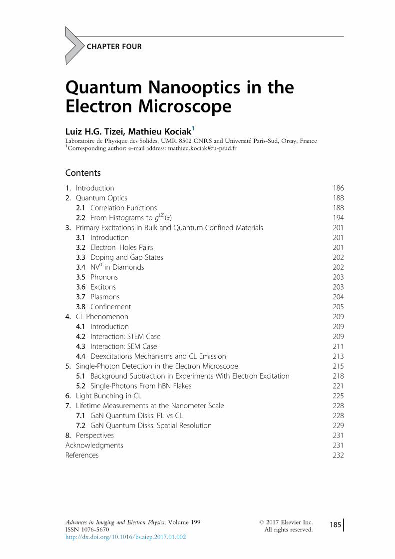
CHAPTER FOUR
Quantum Nanooptics in theElectron MicroscopeLuiz H.G. Tizei, Mathieu Kociak1Laboratoire de Physique des Solides, UMR 8502 CNRS and Universit!e Paris-Sud, Orsay, France1Corresponding author: e-mail address: [email protected]
Contents
1. Introduction 1862. Quantum Optics 188
2.1 Correlation Functions 1882.2 From Histograms to g(2)(τ) 194
3. Primary Excitations in Bulk and Quantum-Confined Materials 2013.1 Introduction 2013.2 Electron–Holes Pairs 2013.3 Doping and Gap States 2023.4 NV0 in Diamonds 2023.5 Phonons 2033.6 Excitons 2033.7 Plasmons 2043.8 Confinement 205
4. CL Phenomenon 2094.1 Introduction 2094.2 Interaction: STEM Case 2094.3 Interaction: SEM Case 2114.4 Deexcitations Mechanisms and CL Emission 213
5. Single-Photon Detection in the Electron Microscope 2155.1 Background Subtraction in Experiments With Electron Excitation 2185.2 Single-Photons From hBN Flakes 221
6. Light Bunching in CL 2257. Lifetime Measurements at the Nanometer Scale 228
7.1 GaN Quantum Disks: PL vs CL 2287.2 GaN Quantum Disks: Spatial Resolution 229
8. Perspectives 231Acknowledgments 231References 232
Advances in Imaging and Electron Physics, Volume 199 # 2017 Elsevier Inc.ISSN 1076-5670 All rights reserved.http://dx.doi.org/10.1016/bs.aiep.2017.01.002
185
1. INTRODUCTION
Quantumoptics concerns optical phenomena that cannot be described
without taking into account the wave-particle duality. As ironically stated by
Lamb (1995) in an interesting discussion, there are only very few situations
where using the concept of photon is relevant.Onemajor exception happens
when a system is sufficiently confined to exhibit a discrete number of elec-
tronic levels. If one considers only the fundamental and first excited states (see
Fig. 1A), the system can be simplified as a two-level system (TLS). Such a
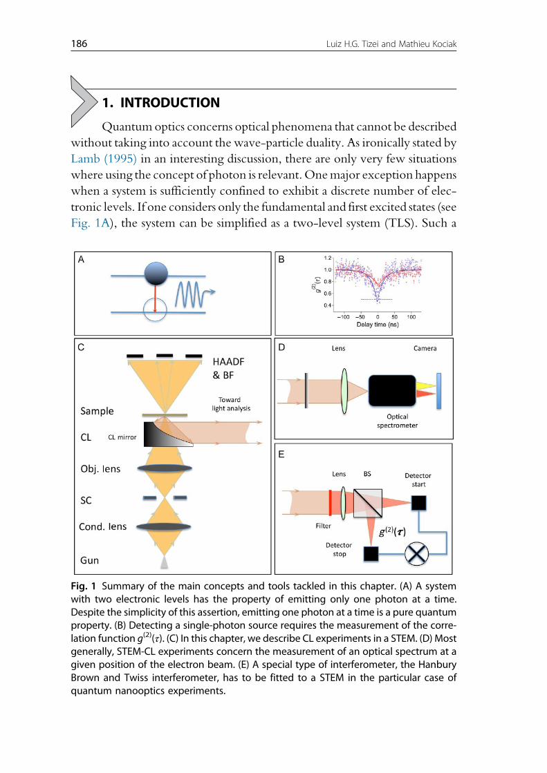
Fig. 1 Summary of the main concepts and tools tackled in this chapter. (A) A systemwith two electronic levels has the property of emitting only one photon at a time.Despite the simplicity of this assertion, emitting one photon at a time is a pure quantumproperty. (B) Detecting a single-photon source requires the measurement of the corre-lation function g(2)(τ). (C) In this chapter, we describe CL experiments in a STEM. (D) Mostgenerally, STEM-CL experiments concern the measurement of an optical spectrum at agiven position of the electron beam. (E) A special type of interferometer, the HanburyBrown and Twiss interferometer, has to be fitted to a STEM in the particular case ofquantum nanooptics experiments.
186 Luiz H.G. Tizei and Mathieu Kociak
system can emit only one photon at a time and is therefore an ideal single-
photon emitter (SPE). SPEs are finding important applications in quantum
cryptography. Typical realizations of SPEs are atoms, quantum dots, mole-
cules, or point defects in semiconductors. The nitrogen vacancy (NV) dis-
cussed further is probably the most studied SPE.
Characterizing an emitter as being an SPE cannot be done by measuring
the first-order properties of light, such as its spectrum. It requires the mea-
surement of the statistical properties of the light coming out of the emitter.
This can be done by measuring the second-order correlation function g(2)(τ),as shown in Fig. 1B. The study and quest for new SPEs is a very fertile field in
which most of the experimental studies relies on the use of photo-
luminescence (PL) to measure g(2)(τ). This technique is obviously diffractionlimited, while the SPEs are all very small compared to the wavelength of
light they emit, as they rely on large electron–hole confinement. Therefore,
subwavelength techniques are desirable. Cathodoluminescence (CL) in a
scanning electron microscope (SEM; Edwards & Martin, 2011; Yacobi &
Holt, 1990) and especially in a scanning transmission electron microscope
(STEM; Kociak & Zagonel, 2017; Yamamoto, Araya, & de Abajo, 2001;
Zagonel et al., 2011) (as depicted in Fig. 1C) has shown great success in map-
ping optical excitations at deep subwavelength resolution, by using spectral
imaging (SI) techniques (Fig. 1D). It is thus tempting to fit the typical appa-
ratus for g(2)(τ) measurements, namely the Hanbury Brown and Twiss
(HBT) intensity interferometer depicted in Fig. 1D, to a STEM-CL appa-
ratus. This has been recently successfully done (Tizei & Kociak, 2013).
Quantum nanooptics with free-electron beams is therefore possible.
However, at the time of writing, only our team has developed tools and
methodology to perform these experiments, although promising develop-
ments are underway in other teams. It is therefore the aim of this chapter
to guide electron microscopists into the fascinating realm of quantum
nanooptics with the hope this will trigger new and exciting discoveries in
this emerging field. With this aim, we first introduce the basics concepts
and instrumentation necessary to apprehend quantum nanooptics in an
EM. However, we assume the reader familiar with the basics of electron
spectromicroscopy (Egerton, 1996; Kociak, St!ephan, Walls, & Colliex,
2011; Kociak & Zagonel, 2017). We then introduce the main electronic
excitations and mechanisms responsible for CL emission, allowing a deeper
understanding of the properties of g(2)(τ), which are not always similar to the
one measured in PL.We then review recent results on the detection of SPEs
(Bourrellier et al., 2016; Tizei & Kociak, 2013), and the difference between
187Quantum Nanooptics in the Electron Microscope
statistics of photons emitted through CL and PL (Meuret et al., 2015).
Finally, this difference allows the determination of nanometer-sized emit-
ters’ lifetime, and we describe this unexpected application of g(2)(τ) measure-
ments (Meuret et al., 2016).
2. QUANTUM OPTICS
There are many well-established texts on general quantum optics
(Fox, 2006; Loudon, 2000). Our aim here is to give sufficient elements
of quantum optics to allow the reader to follow the rest of the text. We will
start by an introduction to correlation functions in Section 2.1. After that,
we will discuss the use of the second-order correlation function, g(2)(τ), tocharacterize different states of light, including classical chaotic (an atom dis-
charge lamp), Poissonian (a laser beam), and number states (a single-photon
beam). This will be followed by a description of how the g(2)(τ) might be
measured using a Hanbury Brown and Twiss interferometer (Section 2.2)
2.1 Correlation FunctionsCorrelation functions of signals in time give important information about
their statistical properties. In quantum optics these functions allow one to
distinguish light beams with different coherence and temporal properties.
In general terms, they are the convolution (of different orders) of the electric
field of a light field at different times (the correlation function might also
include spatial dependences which we omit here). The normalized
first-order correlation function of a light beam is defined as
gð1ÞðτÞ¼ hE*ðtÞEðt + τÞihE*ðtÞEðtÞi
(1)
with E(t) is the electric field at time t, τ is the delay and
hE*ðtÞEðt+ τÞi¼ 1
T
Z
T
E*ðtÞEðt+ τÞdt: (2)
This function measures the first-order coherence of the light field and
gives information, for example, about classical interference effects (such as
observed in a Michelson–Morley interferometer).
A correlation function which has more interest in this discussion is the
normalized second-order correlation function, which is defined as:
188 Luiz H.G. Tizei and Mathieu Kociak
gð2ÞðτÞ¼ hE*ðtÞE*ðt + τÞEðt+ τÞEðtÞihE*ðtÞEðtÞi2
¼ hIðtÞIðt+ τÞihIðtÞi2
, (3)
taking I(t)¼ E*(t)E(t). In simple terms, this function measures the degree of
correlation between the intensity of a light beam measured at two different
times separated by the delay τ.One can gain insight into the physical meaning of this function
by rewriting the intensity as I(t) ¼ I + ΔI(t), with I the temporal average
of the intensity and ΔI the fluctuation from the average at time t (with
average 0):
gð2ÞðτÞ ¼ hðI +ΔIðtÞÞðI +ΔIðt+ τÞÞihðI +ΔIðtÞÞi2
¼ hI2 + IhΔIðtÞi+ IhΔIðt + τÞi+ hΔIðtÞΔIðt + τÞiiI2
¼ hI2 + hΔIðtÞΔIðt + τÞiiI2
,
(4)
as hΔI(t)i¼ 0. First of all, one expects that for large time delays (in fact, larger
than the coherence time of the beam, τc) the fluctuations from the average
are uncorrelated hΔI(t)ΔI(t + τ))i ¼ 0. Therefore:
gð2Þðτ>> τcÞ¼I2
I2¼ 1: (5)
Moreover, it can be shown that for any classical I(t) the average of the
square of the intensity, hI(t)2i, is larger or equal to the square of the average,
hI(t)i2 (Fox, 2006). Hence
gð2ÞðτÞ$ 1 (6)
and
gð2Þð0Þ$ gð2ÞðτÞ: (7)
A simple hands-waving argument to support Eqs. (6) and (7) is that for a
time varying I(t) the fluctuations will have positive and negative values,
which will add up when squared. Hence (6) must be true. As the correlation
between the fluctuation decreases for increasing time delay, g(2)(τ) must also
decrease, leading to inequality (7). In the next three subsections we will
compute this function for three different light beams: a chaotic beam, a
coherent beam, and a single-photon beam (number state).
189Quantum Nanooptics in the Electron Microscope
2.1.1 Chaotic Beam: Classical LightA classical light beam typically has a small coherence time. A prototypical
example is an atom discharge lamp. The phase between the light emitted
from a given atom is randomized by its collisions with other atoms in the
gas. In this section we will calculate the expected g(2)(τ) function, startingfrom the g(1)(τ) function, for this light source and interpret its physical mean-
ing following the description of Loudon (2000). The general behavior of all
light sources we encounter routinely, with the exception of lasers, can be
interpreted in view of this model.
The electric field emitted by an atom in this lamp is
EðtÞ¼E0e%iðω0t%ϕðtÞÞ, (8)
where ϕ(t) is a random phase that is added at each collision (which occurs at
random times).
To calculate the first-order correlation function, we need to compute the
product hE*(t)E(t + τ)i
hE*ðtÞEðt+ τÞi¼E20e
%iω0thfe%iϕ1ðtÞ + e%iϕ2ðtÞ +⋯+ e%iϕN ðtÞg&fe%iϕ1ðt+ τÞ + e%iϕ2ðt+ τÞ +⋯+ e%iϕN ðt+ τÞgi: (9)
with ϕi(t) the random phase added to each atom i at time t. The product of
the phase terms from different atoms is uncorrelated and gives a zero average,
so only the terms from the same atom contribute:
hE*ðtÞEðt + τÞi ¼E20e
%iω0tXN
i¼1
heiðϕiðt+ τÞ%ϕiðtÞi
¼NhE*i ðtÞEiðt+ τÞi:
(10)
As the phase ϕi is a random value added at each atomic collision, only the
field emitted between atomic collisions will contribute to the average in the
last term above. Hence, the correlation will be proportional to the proba-
bility of observing an event after a delay τ between atomic collisions
(Loudon, 2000):
hE*i ðtÞEiðt+ τÞi¼E2
0e%iω0t
Z ∞
τdτ0pðτ0Þ, (11)
with pðτÞdτ¼ð1=τcÞe%τ=τc dτ, τc the typical time between collisions, for pos-
itive values of τ. For atom i:
hE*i ðtÞEiðt+ τÞi¼E2
0e%ðiω0τ%τ=τcÞ: (12)
190 Luiz H.G. Tizei and Mathieu Kociak
So the first-order correlation function for a collision broadened source:
gð1ÞðτÞ¼ e%iω0τe%ðjτj=τcÞ, (13)
using the fact that g(1)(%τ) ¼ g(1)(τ)*. It can be shown that:
gð2ÞðτÞ¼ 1+ jgð1ÞðτÞj2 (14)
and therefore:
gð2ÞðτÞ¼ 1+ e%ð2jτj=τcÞ: (15)
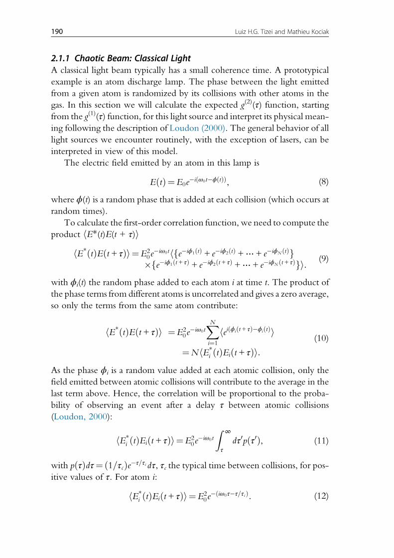
Using Eq. (15) we can check that lim τ!∞gð2ÞðτÞ¼ 1, g(2)(τ) > 18τ and
establish that g(2)(0) ¼ 2, a result valid for all classical light. The shape of this
function is shown in Fig. 2. One can clearly see that a peak appears at low
values of τ. The presence of intensity correlations indicates that there is a
probability of detecting groups of photons larger than that expected from
Poisson statistics. The observation of these correlations for light is called light
bunching and is in strike contrast with what we will discuss for single photons.
Before we continue, it is worth noting that the expected coherence time
for classical light is of the order of femtoseconds. Therefore the width of
bunching peak for this kind of light should be of the order of femtoseconds.
This number should be kept in mind for the discussion in Section 6, where
we will describe the observation of light bunching in CL experiments.
Fig. 2 g(2)(τ) function for a collision broadened classical source, which follows Eq. (2).The time delay τ was normalized by τc.
191Quantum Nanooptics in the Electron Microscope
2.1.2 Coherence Beam: A LaserAn ideal laser is a monochromatic source of light fundamentally character-
ized by its long temporal coherence. The electric field of a laser beam can be
modeled by a sine wave, E0sin(kx % ωt). This electric field has a constant
average intensity over multiple optical cycles, I0. For this reason, one can
readily see that:
gð2ÞðτÞ¼ hIðtÞIðt + τÞihIðtÞi2
¼ I20I20¼ 1, (16)
for all τ. This result can be seen also as the limit of equation (15) for infinitely
long coherence times.
However, this is not equivalent to stating that an instantaneous measure-
ment of the intensity (or the number of photons in the beam) always results
in the same value. In fact, it can be shown that for a laser beam of constant
intensity the probability of detecting n photons follows the Poisson distribu-
tion. Hence the standard deviation of the average is Δn¼ n12.
Eq. (16) is quite important for the normalization of the histograms mea-
sured in intensity interferometry experiments (Section 2.2). Fundamentally,
we assume that at large time delays photon detections are uncorrelated and
follow Poisson statistics. Therefore, a laser source can be used as a reference
for g(2)(τ) normalization (before or after the actual experiment).
2.1.3 Single-Photon Beam: Number StateA single-photon light beam is essentially different from the two types of light
described previously. In simple terms, such a beam is constituted of individ-
ual photons separated by some time delay. In this case, at any time, no more
than one photon can be detected in the beam. At first sight, one could envi-
sion using an attenuated laser as a source of single photons. However, this is
fundamentally wrong, as even in the limit of extremely low intensities the
probability of observing n ¼ 2 is nonzero, given the Poisson statistics of the
photon distribution in a laser beam. Therefore, a completely different
approach is needed.
An alternative idea is to use a highly nonlinear system, which can only be
excited once and that emits only one photon upon deexcitation (Fig. 3).
Such a simple system will emit at most a photon once every excitation/
deexcitation cycle, even if continuously excited. One possibility to realize
this model in practice is to use the energy levels in individual atoms. The
first experimental report of single-photon emission occurred in the late
192 Luiz H.G. Tizei and Mathieu Kociak
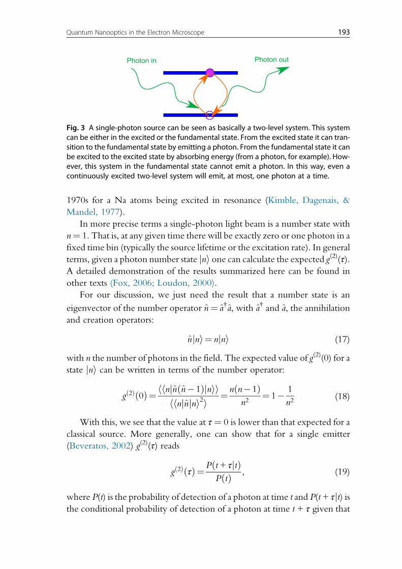
1970s for a Na atoms being excited in resonance (Kimble, Dagenais, &
Mandel, 1977).
In more precise terms a single-photon light beam is a number state with
n¼ 1. That is, at any given time there will be exactly zero or one photon in a
fixed time bin (typically the source lifetime or the excitation rate). In general
terms, given a photon number state jni one can calculate the expected g(2)(τ).A detailed demonstration of the results summarized here can be found in
other texts (Fox, 2006; Loudon, 2000).
For our discussion, we just need the result that a number state is an
eigenvector of the number operator n¼ a{a, with a{ and a, the annihilation
and creation operators:
njni¼ njni (17)
with n the number of photons in the field. The expected value of g(2)(0) for a
state jni can be written in terms of the number operator:
gð2Þð0Þ¼ hhnjnðn%1Þjniihhnjnjni2i
¼ nðn%1Þn2
¼ 1% 1
n2(18)
With this, we see that the value at τ ¼ 0 is lower than that expected for a
classical source. More generally, one can show that for a single emitter
(Beveratos, 2002) g(2)(τ) reads
gð2ÞðτÞ¼Pðt+ τjtÞPðtÞ
, (19)
where P(t) is the probability of detection of a photon at time t and P(t+ τjt) isthe conditional probability of detection of a photon at time t + τ given that
Photon in Photon out
Fig. 3 A single-photon source can be seen as basically a two-level system. This systemcan be either in the excited or the fundamental state. From the excited state it can tran-sition to the fundamental state by emitting a photon. From the fundamental state it canbe excited to the excited state by absorbing energy (from a photon, for example). How-ever, this system in the fundamental state cannot emit a photon. In this way, even acontinuously excited two-level system will emit, at most, one photon at a time.
193Quantum Nanooptics in the Electron Microscope
one was detected at t, which are proportional to the occupation of the
excited state σe(t) (Beveratos, 2002). The population of the excited state
is basically determined by the state lifetime, if the pumping rate is much
smaller than the inverse of the lifetime. In this limit:
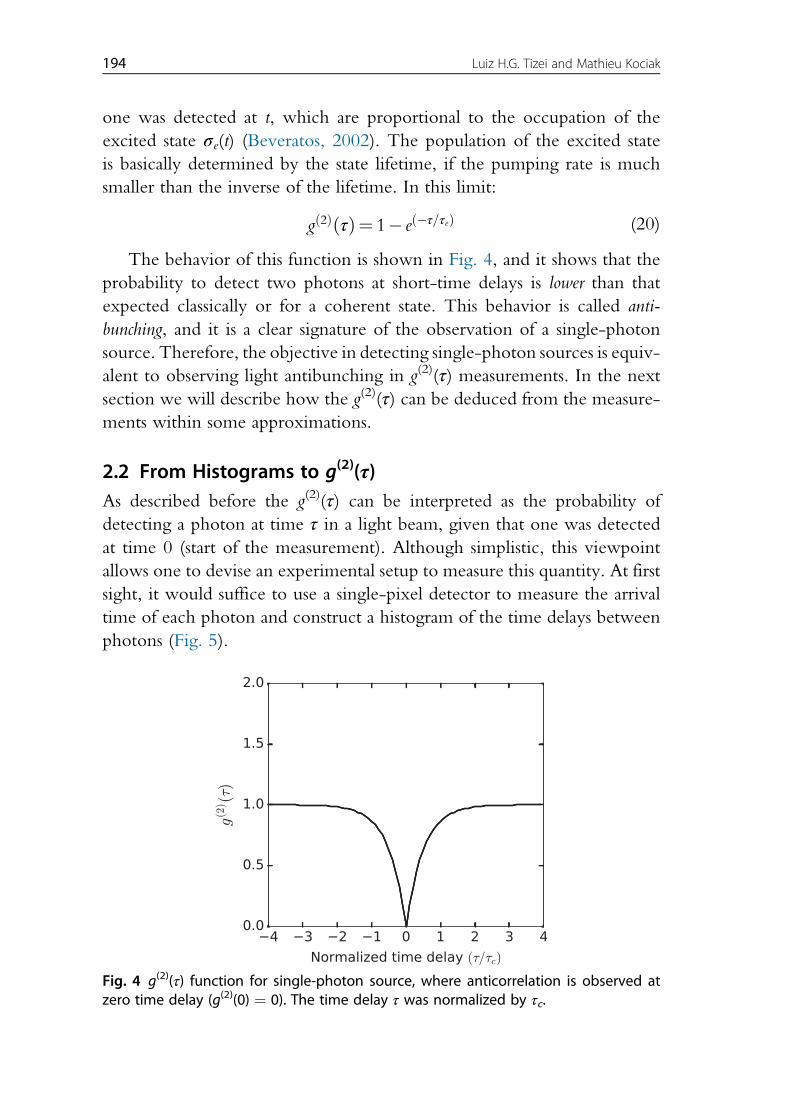
gð2ÞðτÞ¼ 1% eð%τ=τeÞ (20)
The behavior of this function is shown in Fig. 4, and it shows that the
probability to detect two photons at short-time delays is lower than that
expected classically or for a coherent state. This behavior is called anti-
bunching, and it is a clear signature of the observation of a single-photon
source. Therefore, the objective in detecting single-photon sources is equiv-
alent to observing light antibunching in g(2)(τ) measurements. In the next
section we will describe how the g(2)(τ) can be deduced from the measure-
ments within some approximations.
2.2 From Histograms to g(2)(τ)As described before the g(2)(τ) can be interpreted as the probability of
detecting a photon at time τ in a light beam, given that one was detected
at time 0 (start of the measurement). Although simplistic, this viewpoint
allows one to devise an experimental setup to measure this quantity. At first
sight, it would suffice to use a single-pixel detector to measure the arrival
time of each photon and construct a histogram of the time delays between
photons (Fig. 5).
Fig. 4 g(2)(τ) function for single-photon source, where anticorrelation is observed atzero time delay (g(2)(0) ¼ 0). The time delay τ was normalized by τc.
194 Luiz H.G. Tizei and Mathieu Kociak
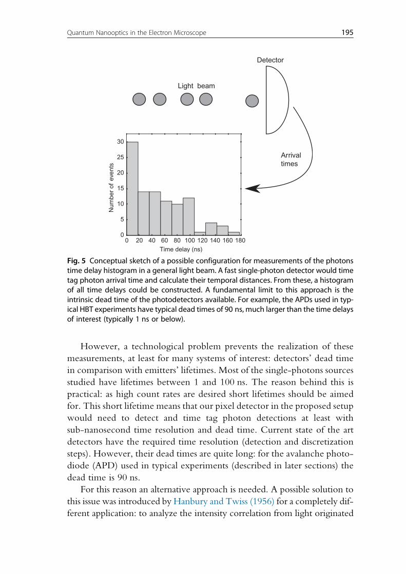
However, a technological problem prevents the realization of these
measurements, at least for many systems of interest: detectors’ dead time
in comparison with emitters’ lifetimes. Most of the single-photons sources
studied have lifetimes between 1 and 100 ns. The reason behind this is
practical: as high count rates are desired short lifetimes should be aimed
for. This short lifetime means that our pixel detector in the proposed setup
would need to detect and time tag photon detections at least with
sub-nanosecond time resolution and dead time. Current state of the art
detectors have the required time resolution (detection and discretization
steps). However, their dead times are quite long: for the avalanche photo-
diode (APD) used in typical experiments (described in later sections) the
dead time is 90 ns.
For this reason an alternative approach is needed. A possible solution to
this issue was introduced by Hanbury and Twiss (1956) for a completely dif-
ferent application: to analyze the intensity correlation from light originated
0 20 40 60 80 100 120 140 160 180Time delay (ns)
0
5
10
15
20
25
30
Num
ber
of e
vent
s
Detector
Arrivaltimes
Light beam
Fig. 5 Conceptual sketch of a possible configuration for measurements of the photonstime delay histogram in a general light beam. A fast single-photon detector would timetag photon arrival time and calculate their temporal distances. From these, a histogramof all time delays could be constructed. A fundamental limit to this approach is theintrinsic dead time of the photodetectors available. For example, the APDs used in typ-ical HBT experiments have typical dead times of 90 ns, much larger than the time delaysof interest (typically 1 ns or below).
195Quantum Nanooptics in the Electron Microscope
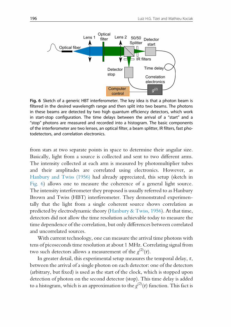
from stars at two separate points in space to determine their angular size.
Basically, light from a source is collected and sent to two different arms.
The intensity collected at each arm is measured by photomultiplier tubes
and their amplitudes are correlated using electronics. However, as
Hanbury and Twiss (1956) had already appreciated, this setup (sketch in
Fig. 6) allows one to measure the coherence of a general light source.
The intensity interferometer they proposed is usually referred to as Hanbury
Brown and Twiss (HBT) interferometer. They demonstrated experimen-
tally that the light from a single coherent source shows correlation as
predicted by electrodynamic theory (Hanbury & Twiss, 1956). At that time,
detectors did not allow the time resolution achievable today to measure the
time dependence of the correlation, but only differences between correlated
and uncorrelated sources.
With current technology, one can measure the arrival time photons with
tens of picoseconds time resolution at about 1 MHz. Correlating signal from
two such detectors allows a measurement of the g(2)(τ).In greater detail, this experimental setup measures the temporal delay, τ,
between the arrival of a single photon on each detector: one of the detectors
(arbitrary, but fixed) is used as the start of the clock, which is stopped upon
detection of photon on the second detector (stop). This time delay is added
to a histogram, which is an approximation to the g(2)(τ) function. This fact is
Optical fiber
Lens 1 Lens 2Optical
filter 50/50Splitter
IR filters
Detectorstart
Detectorstop
Time delay
Correlationelectronics
g(2)Computer control
Fig. 6 Sketch of a generic HBT interferometer. The key idea is that a photon beam isfiltered in the desired wavelength range and then split into two beams. The photonsin these beams are detected by two high quantum efficiency detectors, which workin start-stop configuration. The time delays between the arrival of a “start” and a“stop” photons are measured and recorded into a histogram. The basic componentsof the interferometer are two lenses, an optical filter, a beam splitter, IR filters, fast pho-todetectors, and correlation electronics.
196 Luiz H.G. Tizei and Mathieu Kociak
true if the detection rate is low compared to the detectors’ dead time. Typ-
ically in an experiment count rates per detector are 105 counts/s, so one
event every 10 μs, far slower the detectors’ dead time of 90 ns. This ensures
that time delays longer than the dead time are also probed.
In the next two sections we described the two intensity interferometers
used in the experiments described in later sections.
2.2.1 HBT1—VisibleThe first STEM-CL interferometer was built to detect light from NV0
centers (Tizei & Kociak, 2012, 2013), which emit in a wavelength range
from 575 nm to above 750 nm (phonon tail see Section 5). It was inspired
by regular PL quantum optical setup. The key element in the setup is the
detectors, which are required to have the highest quantum efficiency
(to decrease the measurement time for a correlation function, as it scales
with I2) and with the smallest dead time. One of the best option at the time
of the first HBT experiments in a STEM (Tizei & Kociak, 2013) was ava-
lanche photo diodes (APDs), which are single-pixel detectors with an
active surface 200 μm by 200 μm wide. Other than the small physical size,
this detectors suffer from their sensitivity to high light input (above
1 Mcount/s) when operational. The choice for detectors were τ-SPADs
from Picoquant, which have a quantum efficiency of 70% at 670 nm, a
dead time of 90 ns, a total time jitter of 350 ps (including the detection
electronics). The detection electronics for timing and histogram integra-
tion was a PicoHarp 300, also from PicoQuant, which allows for acquisi-
tion of up to 65536 time delay channels, with time per channel between 4
and 512 ps. The optical part of the interferometer was built to image a sin-
gle input fiber into the two detectors, after a beam splitter (Fig. 6). In this
setup, one images the fiber onto the detectors. As the optical system has no
demagnification, a single 200 μm-core fibers was chosen in relation to the
limited size of the detectors. The fiber possesses an antireflection coating
optimized to the 350–700 nm wavelength range and a numerical aperture
of 0.2. Two lenses (also with antireflection coatings) were used to first pro-
duce a parallel light beam from the fiber input and then focus the light onto
the detectors. Between the two lenses a single passband optical filter
(570–720 nm) was used to limit the light detected to our range of interest.
Finally a 50/50 beam splitter (Thorlabs with antireflection coating in the
350–700 nm wavelength range) was placed after the last lens to separate
evenly the light between both detectors.
197Quantum Nanooptics in the Electron Microscope
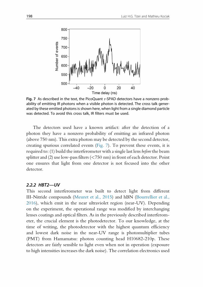
The detectors used have a known artifact: after the detection of a
photon they have a nonzero probability of emitting an infrared photon
(above 750 nm). This extra photon may be detected by the second detector,
creating spurious correlated events (Fig. 7). To prevent these events, it is
required to: (1) build the interferometer with a single last lens before the beam
splitter and (2) use low-pass filters (<750 nm) in front of each detector. Point
one ensures that light from one detector is not focused into the other
detector.
2.2.2 HBT2—UVThis second interferometer was built to detect light from different
III-Nitride compounds (Meuret et al., 2015) and hBN (Bourrellier et al.,
2016), which emit in the near ultraviolet region (near-UV). Depending
on the experiment, the operational range was modified by interchanging
lenses coatings and optical filters. As in the previously described interferom-
eter, the crucial element is the photodetector. To our knowledge, at the
time of writing, the photodetector with the highest quantum efficiency
and lowest dark noise in the near-UV range is photomultiplier tubes
(PMT) from Hamamatsu: photon counting head H10682-210p. These
detectors are fairly sensible to light even when not in operation (exposure
to high intensities increases the dark noise). The correlation electronics used
Fig. 7 As described in the text, the PicoQuant τ-SPAD detectors have a nonzero prob-ability of emitting IR photons when a visible photon is detected. The cross talk gener-ated by these emitted photons is shown here, when light from a single diamond particlewas detected. To avoid this cross talk, IR filters must be used.
198 Luiz H.G. Tizei and Mathieu Kociak
was the same as the one used for the other interferometer (PicoHarp 300).
The input the electronics accepts is a NIM (Nuclear Instrumentation Mod-
ule) signal. The output of the PMTmodules (which include a discriminator)
is a TTL signal. The TTL needs to be converted into NIM using an elec-
tronic board. As the PMT physical detection surface (8 mm) is larger than
that of the APD, an optical fiber with a larger core was used (600 μm) to
facilitate alignment, without any antireflection coating. The optical path
was essentially the same, using lenses and beam-splitters with antireflection
coatings chosen for each desired wavelength range.
This setup can be upgraded to include an optical monochromator to fil-
ter light at shorter wavelength ranges on demand (at the cost of some losses in
total intensity throughput).
2.2.3 Histogram NormalizationAs described before, the time delay histogram measured by an HBT inter-
ferometer is an approximation to the second-order correlation function,
g(2)(τ). One key point in the measurement is the normalization of the his-
togram (Beveratos, 2002). This is done in such a way that for a Poissonian
source g(2)(τ)¼ 1 for all time delays. For a Poissonian source (such as a laser)
the time delay between two photons in the beam is random and equally spa-
ced in time. So, for count rates n1 (counts per second) and n2 in each detector
there should be N2 ¼ TΔτN1N2 counts in a delay window Δτ (the exper-imental time bin size) integrated for time T. Therefore, the normalized his-
togram is given by:
CNorm τð Þ¼ c τð Þn1n2ΔτT
¼ g 2ð Þ τð Þ (21)
where c(τ) is the measured histogram. This is strictly true only for a
Poissonian source. As we discussed in previous sections, light beams with
other temporal dependencies do not respect equation (21) for all τ. How-
ever, correlation effects in the g(2)(τ) function should always decrease for
increasing τ. In this way, for τ>> τc, with τc some typical time of the system
(i.e., a lifetime), the value of g(2)(τ) should tend to 1.
For the experiments described here, the normalization has been per-
formed by assuming that for a long-time delay (typically at least five times
the value of the emitter lifetime) g(2)(τ)¼ 1. This behavior has been checked
using the interferometers described here tomeasure g(2)(τ) for a laser beam. In
Fig. 8A we show a measurement of the photon-pair delay histogram for a
199Quantum Nanooptics in the Electron Microscope
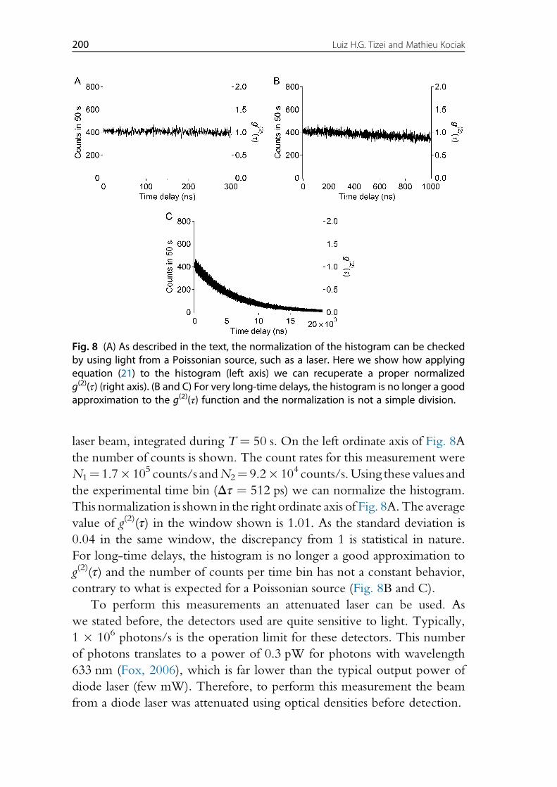
laser beam, integrated during T ¼ 50 s. On the left ordinate axis of Fig. 8A
the number of counts is shown. The count rates for this measurement were
N1¼ 1.7& 105 counts/s andN2¼ 9.2& 104 counts/s.Using these values and
the experimental time bin (Δτ ¼ 512 ps) we can normalize the histogram.
This normalization is shown in the right ordinate axis of Fig. 8A. The average
value of g(2)(τ) in the window shown is 1.01. As the standard deviation is
0.04 in the same window, the discrepancy from 1 is statistical in nature.
For long-time delays, the histogram is no longer a good approximation to
g(2)(τ) and the number of counts per time bin has not a constant behavior,
contrary to what is expected for a Poissonian source (Fig. 8B and C).
To perform this measurements an attenuated laser can be used. As
we stated before, the detectors used are quite sensitive to light. Typically,
1 & 106 photons/s is the operation limit for these detectors. This number
of photons translates to a power of 0.3 pW for photons with wavelength
633 nm (Fox, 2006), which is far lower than the typical output power of
diode laser (few mW). Therefore, to perform this measurement the beam
from a diode laser was attenuated using optical densities before detection.
Fig. 8 (A) As described in the text, the normalization of the histogram can be checkedby using light from a Poissonian source, such as a laser. Here we show how applyingequation (21) to the histogram (left axis) we can recuperate a proper normalizedg(2)(τ) (right axis). (B and C) For very long-time delays, the histogram is no longer a goodapproximation to the g(2)(τ) function and the normalization is not a simple division.
200 Luiz H.G. Tizei and Mathieu Kociak
3. PRIMARY EXCITATIONS IN BULK ANDQUANTUM-CONFINED MATERIALS
3.1 IntroductionIn this section, we review the most important solid-state excitations relevant
for the study of CL; mechanisms of light production under electron beam
irradiation that totally depend on these excitations are described in the fol-
lowing section. The physics of basic excitations in semiconductors and the
related emission have been introduced in many textbooks, among which
Fox (2010) and Peter and Cardona (2010) have to be highlighted. Applica-
tions to CL and discussion of the electron–matter interaction have been
tackled in the reference book of Yacobi and Holt (1990), and in more details
in the case of the STEM-CL in a recent review (Kociak & Zagonel, 2017).
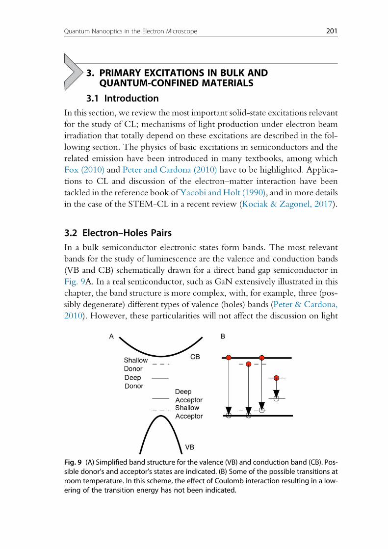
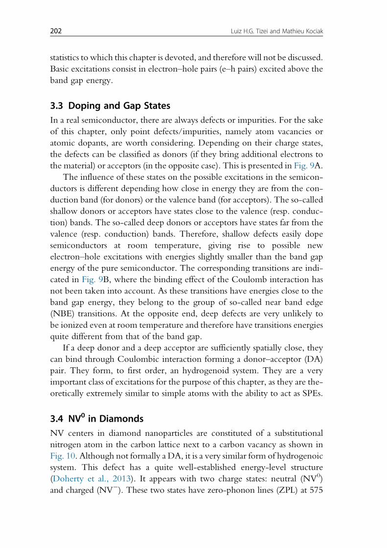
3.2 Electron–Holes PairsIn a bulk semiconductor electronic states form bands. The most relevant
bands for the study of luminescence are the valence and conduction bands
(VB and CB) schematically drawn for a direct band gap semiconductor in
Fig. 9A. In a real semiconductor, such as GaN extensively illustrated in this
chapter, the band structure is more complex, with, for example, three (pos-
sibly degenerate) different types of valence (holes) bands (Peter & Cardona,
2010). However, these particularities will not affect the discussion on light
Fig. 9 (A) Simplified band structure for the valence (VB) and conduction band (CB). Pos-sible donor’s and acceptor’s states are indicated. (B) Some of the possible transitions atroom temperature. In this scheme, the effect of Coulomb interaction resulting in a low-ering of the transition energy has not been indicated.
201Quantum Nanooptics in the Electron Microscope
statistics to which this chapter is devoted, and therefore will not be discussed.
Basic excitations consist in electron–hole pairs (e–h pairs) excited above the
band gap energy.
3.3 Doping and Gap StatesIn a real semiconductor, there are always defects or impurities. For the sake
of this chapter, only point defects/impurities, namely atom vacancies or
atomic dopants, are worth considering. Depending on their charge states,
the defects can be classified as donors (if they bring additional electrons to
the material) or acceptors (in the opposite case). This is presented in Fig. 9A.
The influence of these states on the possible excitations in the semicon-
ductors is different depending how close in energy they are from the con-
duction band (for donors) or the valence band (for acceptors). The so-called
shallow donors or acceptors have states close to the valence (resp. conduc-
tion) bands. The so-called deep donors or acceptors have states far from the
valence (resp. conduction) bands. Therefore, shallow defects easily dope
semiconductors at room temperature, giving rise to possible new
electron–hole excitations with energies slightly smaller than the band gap
energy of the pure semiconductor. The corresponding transitions are indi-
cated in Fig. 9B, where the binding effect of the Coulomb interaction has
not been taken into account. As these transitions have energies close to the
band gap energy, they belong to the group of so-called near band edge
(NBE) transitions. At the opposite end, deep defects are very unlikely to
be ionized even at room temperature and therefore have transitions energies
quite different from that of the band gap.
If a deep donor and a deep acceptor are sufficiently spatially close, they
can bind through Coulombic interaction forming a donor–acceptor (DA)
pair. They form, to first order, an hydrogenoid system. They are a very
important class of excitations for the purpose of this chapter, as they are the-
oretically extremely similar to simple atoms with the ability to act as SPEs.
3.4 NV0 in DiamondsNV centers in diamond nanoparticles are constituted of a substitutional
nitrogen atom in the carbon lattice next to a carbon vacancy as shown in
Fig. 10. Although not formally a DA, it is a very similar form of hydrogenoic
system. This defect has a quite well-established energy-level structure
(Doherty et al., 2013). It appears with two charge states: neutral (NV0)
and charged (NV%). These two states have zero-phonon lines (ZPL) at 575
202 Luiz H.G. Tizei and Mathieu Kociak
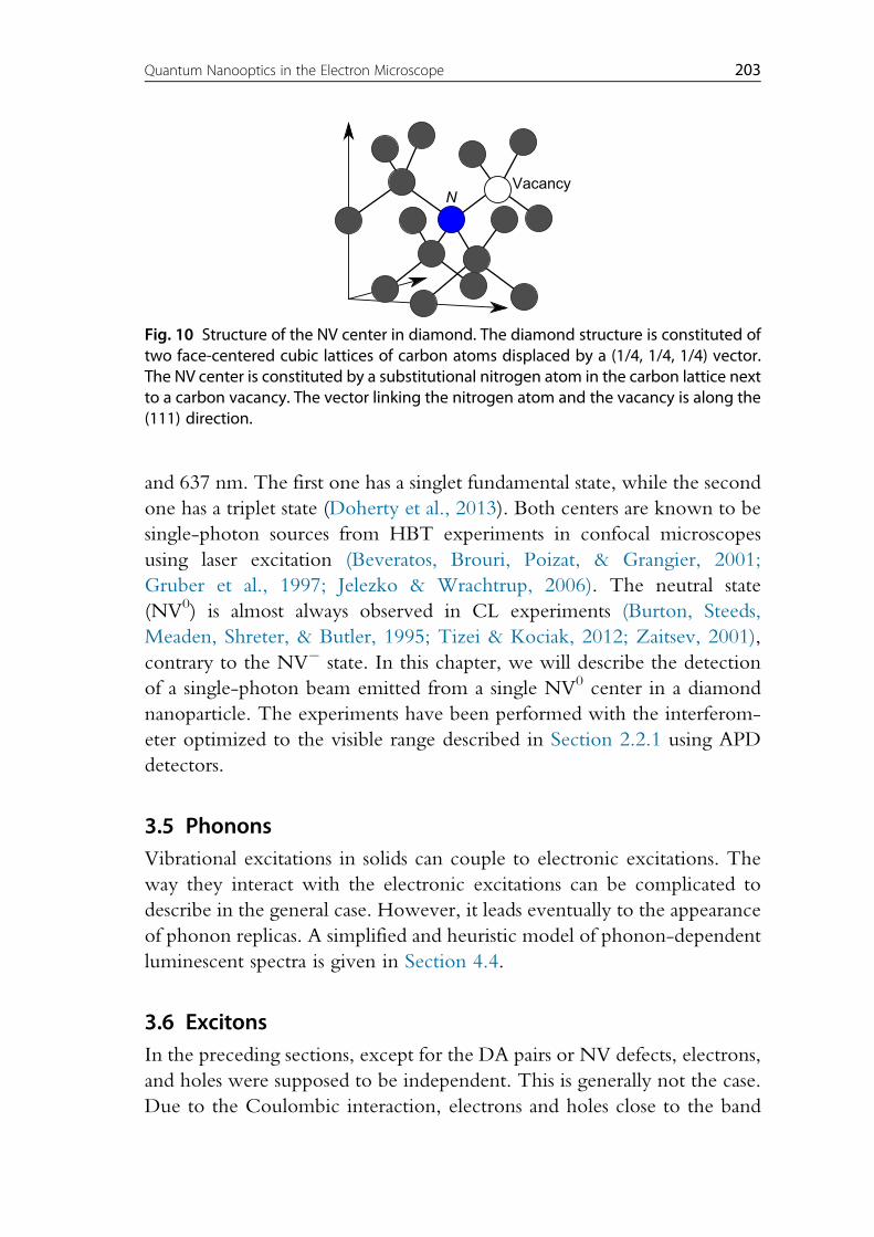
and 637 nm. The first one has a singlet fundamental state, while the second
one has a triplet state (Doherty et al., 2013). Both centers are known to be
single-photon sources from HBT experiments in confocal microscopes
using laser excitation (Beveratos, Brouri, Poizat, & Grangier, 2001;
Gruber et al., 1997; Jelezko & Wrachtrup, 2006). The neutral state
(NV0) is almost always observed in CL experiments (Burton, Steeds,
Meaden, Shreter, & Butler, 1995; Tizei & Kociak, 2012; Zaitsev, 2001),
contrary to the NV% state. In this chapter, we will describe the detection
of a single-photon beam emitted from a single NV0 center in a diamond
nanoparticle. The experiments have been performed with the interferom-
eter optimized to the visible range described in Section 2.2.1 using APD
detectors.
3.5 PhononsVibrational excitations in solids can couple to electronic excitations. The
way they interact with the electronic excitations can be complicated to
describe in the general case. However, it leads eventually to the appearance
of phonon replicas. A simplified and heuristic model of phonon-dependent
luminescent spectra is given in Section 4.4.
3.6 ExcitonsIn the preceding sections, except for the DA pairs or NV defects, electrons,
and holes were supposed to be independent. This is generally not the case.
Due to the Coulombic interaction, electrons and holes close to the band
NVacancy
Fig. 10 Structure of the NV center in diamond. The diamond structure is constituted oftwo face-centered cubic lattices of carbon atoms displaced by a (1/4, 1/4, 1/4) vector.The NV center is constituted by a substitutional nitrogen atom in the carbon lattice nextto a carbon vacancy. The vector linking the nitrogen atom and the vacancy is along the(111) direction.
203Quantum Nanooptics in the Electron Microscope
edges will interact to form hydrogenic-like systems, much like DA pairs do.
However, in semiconductors, the Coulombic interaction is usually strongly
screened, and the binding is small. Typical binding energies Eb are 20 meV
for GaN (Sieber, 2016). In the materials (GaN) considered here, the binding
energy is larger than the temperature of liquid nitrogen divided by the
Boltzmann constant. This ensures that even in the bulk materials, excitons
may exist (see the case of quantum-confined system later in Section 3.8) at
these temperatures. At temperatures higher than Eb/kbT, the exciton gets
ionized, and we are left with unbound e–h pairs.We note that different exci-
tons correspond to the different electron–hole transitions described in
Fig. 9B. For example, the exciton formed by an electron in the conduction
band and an hole in the valence band will be called free-exciton; its energy
will be that of the band gap minored by the binding energy. Other forms
of excitons that interact with donors or acceptors may exist. They usually
have even smaller energies than the free-exciton or the equivalent unbound
NBE transitions.
3.7 Plasmons3.7.1 Bulk PlasmonsIn a finer description of the excitations of solid-state materials, a special sort
of excitation has to be discussed. In addition to the aforementioned excita-
tions, bulk plasmons do exist. Bulk plasmons are well known in metals,
where they are described as collective longitudinal acoustic-like waves of
the free-electron gas. This type of excitations also exists in semiconductors
as collective oscillations of the e–h pairs close to the bottom of the conduc-
tion band and the top of the valence band. Typical plasmons energies are
much above the visible range—typically 20–30 eV. Also, their longitudinalcharacter prevents them to couple to light in the far-field. However, we will
see that they play a crucial role for the CL mechanisms.
3.7.2 Surface PlasmonsSurface plasmons are the surface equivalent of bulk plasmon waves. In sev-
eral metals (silver, gold, etc.) they display interesting physics and promising
applications. One of the great success of the CL in the past 20 years has been
the mapping of these waves at deep subwavelength resolution within
metal nanoparticles (Das, Chini, & Pond, 2012; Losquin et al., 2015;
Vesseur, de Waele, Kuttge, & Polman, 2007; Yamamoto et al., 2001).
204 Luiz H.G. Tizei and Mathieu Kociak
However, the typical lifetimes of the surface plasmons in nanoparticles are
sub-picoseconds, so that with the instrumentation described here accessing
their temporal behavior is impossible. Interested readers may refer to
Losquin and Lummen (2017) for a description of alternative techniques
to tackle this issue.
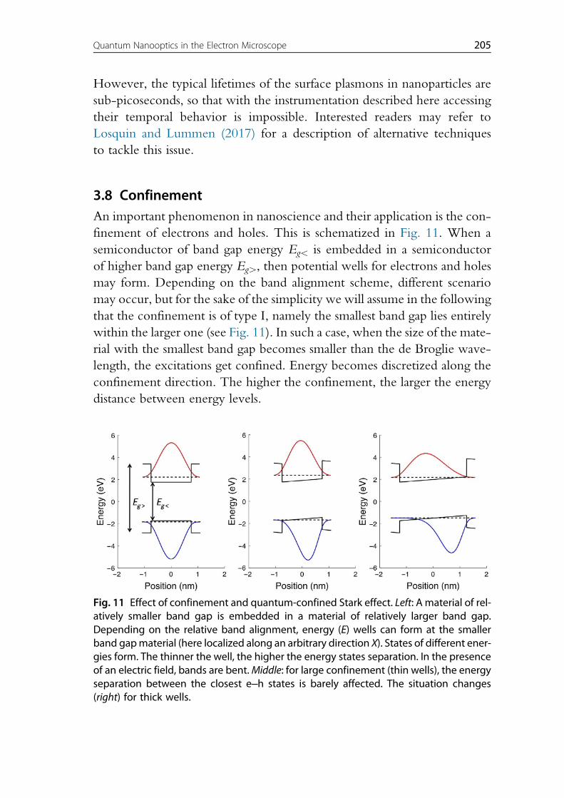
3.8 ConfinementAn important phenomenon in nanoscience and their application is the con-
finement of electrons and holes. This is schematized in Fig. 11. When a
semiconductor of band gap energy Eg< is embedded in a semiconductor
of higher band gap energy Eg>, then potential wells for electrons and holes
may form. Depending on the band alignment scheme, different scenario
may occur, but for the sake of the simplicity we will assume in the following
that the confinement is of type I, namely the smallest band gap lies entirely
within the larger one (see Fig. 11). In such a case, when the size of the mate-
rial with the smallest band gap becomes smaller than the de Broglie wave-
length, the excitations get confined. Energy becomes discretized along the
confinement direction. The higher the confinement, the larger the energy
distance between energy levels.
Fig. 11 Effect of confinement and quantum-confined Stark effect. Left: A material of rel-atively smaller band gap is embedded in a material of relatively larger band gap.Depending on the relative band alignment, energy (E) wells can form at the smallerband gapmaterial (here localized along an arbitrary direction X). States of different ener-gies form. The thinner the well, the higher the energy states separation. In the presenceof an electric field, bands are bent.Middle: for large confinement (thin wells), the energyseparation between the closest e–h states is barely affected. The situation changes(right) for thick wells.
205Quantum Nanooptics in the Electron Microscope
3.8.1 Quantum-Confined Stark EffectIn the presence of an electrical field, the energy bands of a material bend as
schematically shown in Fig. 11, middle. If the bending is relatively small
and the confinement high, the (quantified) electron and hole states are
not essentially modified. However, when the field is high, the energy levels
start to be affected. The effect can be strong enough so that the energy dif-
ferences between the closest e–h states becomes smaller than the band gap
of the bulk material. Moreover, electron and hole states become localized
on opposite sides of the wells, largely decreasing their wavefunctions over-
lap. This effect is called quantum-confined Stark effect (QCSE) (Miller
et al., 1984). Although not ubiquitous, this effect is determinant to the
understanding of the utmost technologically interesting materials made
up of AlGaInN alloys, because it can change the energy and intensity of
the emission by several orders of magnitude (Kalliakos et al., 2004;
Lefebvre, Homma, & Finnie, 2003; Lefebvre & Gayral, 2008). In these
materials, the field, which can be as high as 10 MV/cm, arises from the
pyro- and piezoelectric effects when the material is grown along its polar
direction.
3.8.2 Two-Dimensional ConfinementAn important class of quantum-confined materials are quantumwells (QW),
where the confinement takes place along one dimension only. An important
consequence of bidimensional confinement is the increase of excitonic
binding energy (theoretically a factor of 4). In GaN for example, this leads
to very robust excitonic states.
Such QWs are objects of choice for CL experiments. We report in
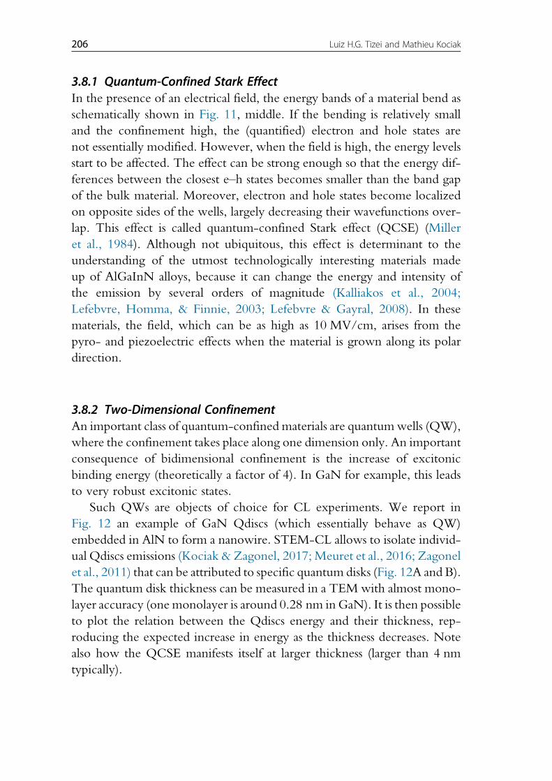
Fig. 12 an example of GaN Qdiscs (which essentially behave as QW)
embedded in AlN to form a nanowire. STEM-CL allows to isolate individ-
ual Qdiscs emissions (Kociak & Zagonel, 2017; Meuret et al., 2016; Zagonel
et al., 2011) that can be attributed to specific quantum disks (Fig. 12A and B).
The quantum disk thickness can be measured in a TEM with almost mono-
layer accuracy (onemonolayer is around 0.28 nm in GaN). It is then possible
to plot the relation between the Qdiscs energy and their thickness, rep-
roducing the expected increase in energy as the thickness decreases. Note
also how the QCSE manifests itself at larger thickness (larger than 4 nm
typically).
206 Luiz H.G. Tizei and Mathieu Kociak
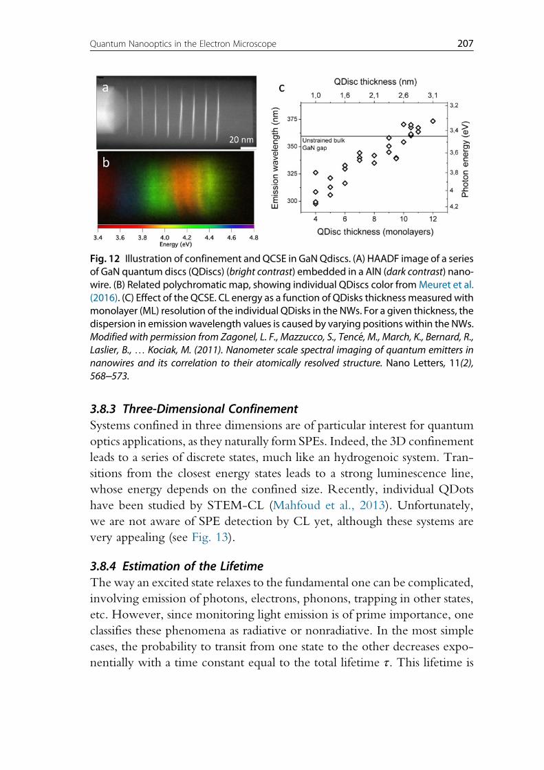
3.8.3 Three-Dimensional ConfinementSystems confined in three dimensions are of particular interest for quantum
optics applications, as they naturally form SPEs. Indeed, the 3D confinement
leads to a series of discrete states, much like an hydrogenoic system. Tran-
sitions from the closest energy states leads to a strong luminescence line,
whose energy depends on the confined size. Recently, individual QDots
have been studied by STEM-CL (Mahfoud et al., 2013). Unfortunately,
we are not aware of SPE detection by CL yet, although these systems are
very appealing (see Fig. 13).
3.8.4 Estimation of the LifetimeThe way an excited state relaxes to the fundamental one can be complicated,
involving emission of photons, electrons, phonons, trapping in other states,
etc. However, since monitoring light emission is of prime importance, one
classifies these phenomena as radiative or nonradiative. In the most simple
cases, the probability to transit from one state to the other decreases expo-
nentially with a time constant equal to the total lifetime τ. This lifetime is
Fig. 12 Illustration of confinement and QCSE in GaNQdiscs. (A) HAADF image of a seriesof GaN quantum discs (QDiscs) (bright contrast) embedded in a AlN (dark contrast) nano-wire. (B) Related polychromatic map, showing individual QDiscs color fromMeuret et al.(2016). (C) Effect of the QCSE. CL energy as a function of QDisks thicknessmeasured withmonolayer (ML) resolution of the individual QDisks in the NWs. For a given thickness, thedispersion in emissionwavelength values is caused by varying positions within the NWs.Modified with permission from Zagonel, L. F., Mazzucco, S., Tenc!e, M., March, K., Bernard, R.,Laslier, B., … Kociak, M. (2011). Nanometer scale spectral imaging of quantum emitters innanowires and its correlation to their atomically resolved structure. Nano Letters, 11(2),568–573.
207Quantum Nanooptics in the Electron Microscope
related to the radiative τR and nonradiative τNR lifetimes through 1/τ ¼1/τR + 1/τNR. For the sake of brevity, we will not discuss the expression
of τNR and oversimplifying the expression τR by noting that in the two main
cases of interest here (quantum-confined systems and SPEs):
1=τR ' jZ
d r!Φeð r!ÞΦhð r!Þj2 (22)
where Φeð r!Þ and Φhð r!Þ are symbolic expressions for the electron and
hole wavefunctions (for example, in reality, the envelope wavefunctions
should be used for quantum-confined systems). The main consequence of
this expression is that the lifetime is increasing with decreasing spatial overlap
of the two wavefunctions involved in the transition.
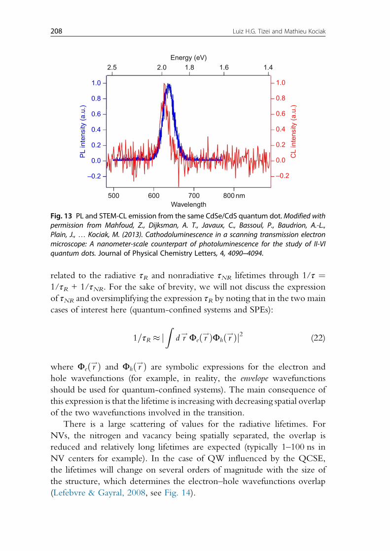
There is a large scattering of values for the radiative lifetimes. For
NVs, the nitrogen and vacancy being spatially separated, the overlap is
reduced and relatively long lifetimes are expected (typically 1–100 ns inNV centers for example). In the case of QW influenced by the QCSE,
the lifetimes will change on several orders of magnitude with the size of
the structure, which determines the electron–hole wavefunctions overlap
(Lefebvre & Gayral, 2008, see Fig. 14).
1.0
2.5 2.0Energy (eV)
1.8 1.6 1.4
0.8
0.6
0.4
0.2
0.0
–0.2
CL
inte
nsity
(a.
u.)
Wavelength
PL
inte
nsity
(a.
u.)
500 600 700 800 nm
–0.2
0.0
0.2
0.4
0.6
0.8
1.0
Fig. 13 PL and STEM-CL emission from the same CdSe/CdS quantum dot.Modified withpermission from Mahfoud, Z., Dijksman, A. T., Javaux, C., Bassoul, P., Baudrion, A.-L.,Plain, J., … Kociak, M. (2013). Cathodoluminescence in a scanning transmission electronmicroscope: A nanometer-scale counterpart of photoluminescence for the study of II-VIquantum dots. Journal of Physical Chemistry Letters, 4, 4090–4094.
208 Luiz H.G. Tizei and Mathieu Kociak
4. CL PHENOMENON4.1 Introduction
For the sake of simplicity, we will start by discussing the case of the
STEM-CL. More details on the STEM-CL can be found in Kociak and
Zagonel (2017). The frontier between STEM and SEM is arbitrary, and
therefore the following has to be interpreted with care. In the following,
we will describe the SEM cases as experiments where the acceleration volt-
age is relatively small (typically few keV, and anyway less than 30 kV), and
sample essentially infinitely thick (in the sense of penetration depth, see
Section 4.3). On the other hand, the STEM-CL case concerns situations
where the high voltage is relatively high (from 60 to 200 kV, 60 kV being
more typical), and is considered as very thin (in the sense of the mean-free
path λe, see Section 4.2).
4.2 Interaction: STEM Case4.2.1 Primary Excitations CreationContrary to PL, where the incoming photon directly creates one electron–hole pair, the process of e–h pair creation is less straightforward in CL.When
a fast electron impinges on a thin material, it interacts elastically and
inelastically. Per definition, only the later interaction is susceptible to transfer
1.5 2.0 2.5 3.0 3.5 4.0
3.5 3.0 2.5Quantum dot height (nm)
2.0 1.5
Energy (eV)
GaN/AIN QDs
11 MV/cm9 MV/cm
7 MV/cm1 ms
1 ns
Rad
iativ
e lif
etim
e
1 µs
Fig. 14 Measured radiative lifetime circles vs measured energy of PL peak for the dif-ferent QD samples. From Lefebvre, P., & Gayral, B. (2008). Optical properties of GaN/AlNquantum dots. Comptes Rendus Physique, 9 (8), 816–829, reprinted with permission.
209Quantum Nanooptics in the Electron Microscope
energy to the material. This energy transfer is, however, usually not large. As
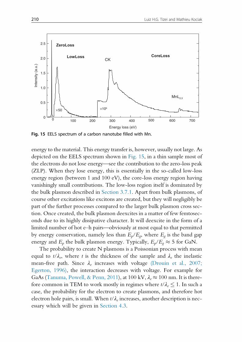
depicted on the EELS spectrum shown in Fig. 15, in a thin sample most of
the electrons do not lose energy—see the contribution to the zero-loss peak
(ZLP). When they lose energy, this is essentially in the so-called low-loss
energy region (between 1 and 100 eV), the core-loss energy region having
vanishingly small contributions. The low-loss region itself is dominated by
the bulk plasmon described in Section 3.7.1. Apart from bulk plasmons, of
course other excitations like excitons are created, but they will negligibly be
part of the further processes compared to the larger bulk plasmon cross sec-
tion. Once created, the bulk plasmon deexcites in a matter of few femtosec-
onds due to its highly dissipative character. It will deexcite in the form of a
limited number of hot e–h pairs—obviously at most equal to that permitted
by energy conservation, namely less than Ep/Eg, where Eg is the band gap
energy and Ep the bulk plasmon energy. Typically, Ep/Eg ' 5 for GaN.
The probability to create N plasmons is a Poissonian process with mean
equal to t/λe, where t is the thickness of the sample and λe the inelastic
mean-free path. Since λe increases with voltage (Drouin et al., 2007;
Egerton, 1996), the interaction decreases with voltage. For example for
GaAs (Tanuma, Powell, & Penn, 2011), at 100 kV, λe' 100 nm. It is there-
fore common in TEM to work mostly in regimes where t/λe ( 1. In such a
case, the probability for the electron to create plasmons, and therefore hot
electron hole pairs, is small. When t/λe increases, another description is nec-essary which will be given in Section 4.3.
× ×
Fig. 15 EELS spectrum of a carbon nanotube filled with Mn.
210 Luiz H.G. Tizei and Mathieu Kociak
4.2.2 Thermalization and DiffusionOnce created, the e–h pairs thermalize in a ps second range to their local
energy minima (Sieber, 2016).
At this time, the e–h pairs (which may be bound in the form of excitons)
start to diffuse until they deexcite radiatively or nonradiatively. Different
types of diffusion are given in Yacobi and Holt (1990). An important
consequence of the diffusion is that STEM- (and SEM-) CL can be seen
as excitation spectromicroscopy: the optical information gained when the
beam is at a particular position comes from all positions around the beam
(where radiative events have taken place). This results in a smoothed imag-
ing, the typical smoothing extension being the diffusion length. This diffu-
sion length will decrease depending on the presence of nonradiative and
radiative recombination centers. Although in high purity materials it can
be very large (e.g., excitons in diamond, Barjon et al., 2011), this is fortu-
nately not the case for many nanoscale structures. Indeed, in
quantum-confined systems, the potential wells themselves often act as effec-
tive e–h traps; also, surfaces (always present at least in the direction perpen-
dicular to the electron beam in the case of STEM-CL) may act as efficient
nonradiative centers, etc. This allows a relatively high spatial resolution in
CL, although largely dependent on the material of interest and its nano-
structuration. This is exemplified in the case GaN Qdiscs (where the reso-
lution can be better than 5 nm, Zagonel, Rigutti, Jacopin, Songmuang, &
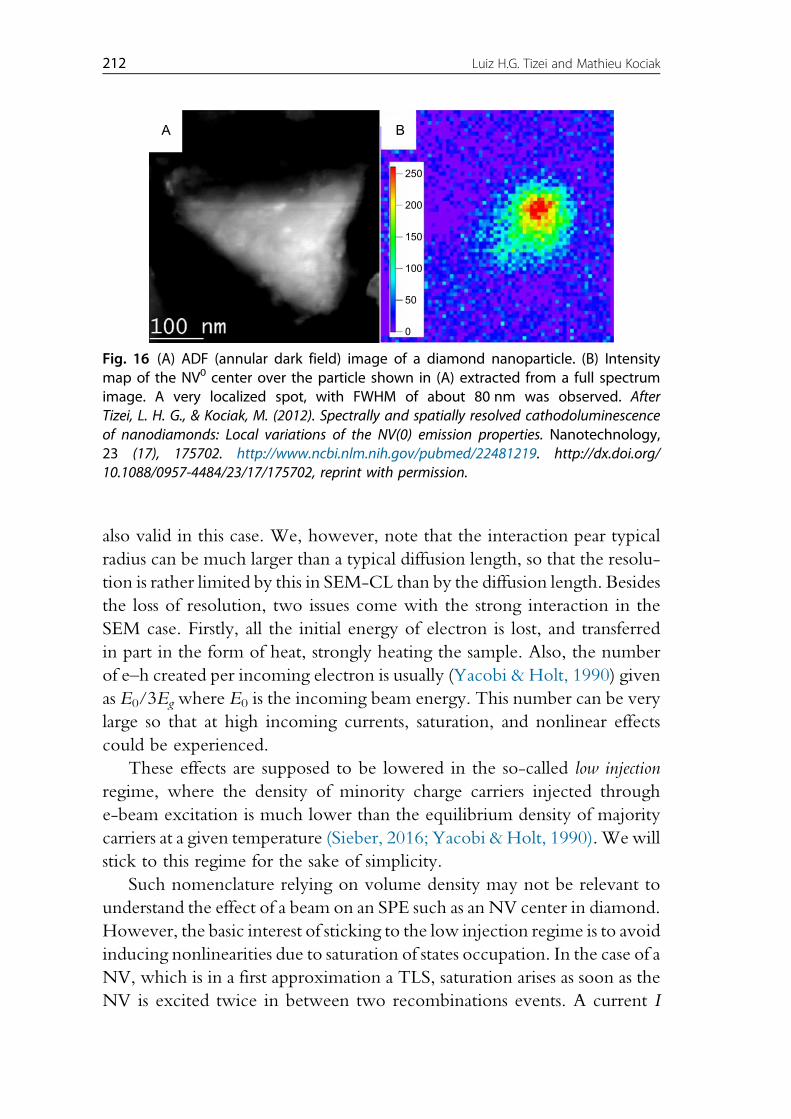
Kociak, 2012) or in the case of NV centers in nanodiamonds (80 nm full
width at half maximum, FWHM, Fig. 16, Tizei & Kociak, 2013).
4.3 Interaction: SEM CaseThe case of SEM-CL has been discussed in many books (Sieber, 2016;
Yacobi & Holt, 1990). In this thick sample/low voltage regime, the above
description is no longer valid. Of course, the main source of e–h is the exci-tation of hot e–h pairs through multiple bulk plasmons creation. However,
in addition to inelastic scattering, the incoming electrons suffer from strong
elastic interaction. Even for arbitrarily small incoming beam diameters, the
electrons will spread over a large volume, known as the interaction pear. The
radius of such a pear can be as large as few microns at kV accelerating volt-
ages. The incoming electron will lose all its energy while being scattered in
the material and eventually stopped, so that the most relevant length in this
case is not the mean-free path but rather the penetration length (Yacobi &
Holt, 1990). All the other mechanisms of thermalization and diffusion are
211Quantum Nanooptics in the Electron Microscope
also valid in this case. We, however, note that the interaction pear typical
radius can be much larger than a typical diffusion length, so that the resolu-
tion is rather limited by this in SEM-CL than by the diffusion length. Besides
the loss of resolution, two issues come with the strong interaction in the
SEM case. Firstly, all the initial energy of electron is lost, and transferred
in part in the form of heat, strongly heating the sample. Also, the number
of e–h created per incoming electron is usually (Yacobi & Holt, 1990) given
as E0/3Eg where E0 is the incoming beam energy. This number can be very
large so that at high incoming currents, saturation, and nonlinear effects
could be experienced.
These effects are supposed to be lowered in the so-called low injection
regime, where the density of minority charge carriers injected through
e-beam excitation is much lower than the equilibrium density of majority
carriers at a given temperature (Sieber, 2016; Yacobi &Holt, 1990).Wewill
stick to this regime for the sake of simplicity.
Such nomenclature relying on volume density may not be relevant to
understand the effect of a beam on an SPE such as an NV center in diamond.
However, the basic interest of sticking to the low injection regime is to avoid
inducing nonlinearities due to saturation of states occupation. In the case of a
NV, which is in a first approximation a TLS, saturation arises as soon as the
NV is excited twice in between two recombinations events. A current I
250
200
150
100
50
0
A B
Fig. 16 (A) ADF (annular dark field) image of a diamond nanoparticle. (B) Intensitymap of the NV0 center over the particle shown in (A) extracted from a full spectrumimage. A very localized spot, with FWHM of about 80 nm was observed. AfterTizei, L. H. G., & Kociak, M. (2012). Spectrally and spatially resolved cathodoluminescenceof nanodiamonds: Local variations of the NV(0) emission properties. Nanotechnology,23 (17), 175702. http://www.ncbi.nlm.nih.gov/pubmed/22481219. http://dx.doi.org/10.1088/0957-4484/23/17/175702, reprint with permission.
212 Luiz H.G. Tizei and Mathieu Kociak
corresponds to the production of N ¼ t/λeαIτ/e e–h pairs, where α is the
number of e–h pairs created by plasmon, and e is the magnitude of the elec-
tron charge. This is of course neglecting the exponentially decreasing num-
ber of e–h reaching the NV when it is away from the injection position.
A moderate I¼ 10pA creates during a lifetime τ¼ 1ns. With a typical thick-
ness to mean-free path ratio of 0.1,N' 0.1 * 5 * 10%11 * 10%9/(1.6 * 10%19)
' 0.03 e–h pairs as a upper estimate. This is a very rough estimate as it totally
neglects the effect of diffusion which will lower this number extremely rap-
idly. This explains that saturation of individual NV or other individual point
defect has never been reported to the best of our knowledge in STEM-CL.
4.4 Deexcitations Mechanisms and CL EmissionIn Section 3.8.4, we have dealt with the evaluation of the radiative lifetime,
which essentially follows from the Fermi golden rule. Nonradiative events
can also take place, to which a nonradiative lifetime is attached, so that the
total lifetime 1/τ ¼ 1/τR + 1/τNR. Radiative recombination events can be
either unbound e–h pair recombinations or excitonic recombinations. The
two processes are different—in the unbound case, the minority carrier can
recombine with any other majority carrier; in the excitonic case, the initial
e–h pair has to recombine together. However, in the low injection regime,
the two phenomena cannot be distinguished on the CL intensity. In the two
cases, the CL intensity reads (Sieber, 2016; Yacobi & Holt, 1990):
ICL∝n=τR (23)
with n being either the density of excess minority carriers or the density of
excess excitons. We note that ICL is inversely proportional to the radiative
lifetime, which is not surprising as it is a radiative technique. The former
formula is valid in the stationary regime. However, if one follows the time
evolution of the CL intensity after a pulse excitation, then we should write:
ICLðtÞ∝nðtÞ=τR ¼ n0e%t=τ=τR (24)
with n0 being the density of charge carriers at time 0. The CL intensity
therefore decays exponentially with time, with a time constant equal to
the total lifetime. Otherwise speaking, the CL emission rate (the CL inten-
sity) is inversely proportional to the radiative lifetime for a given density of
charge carrier, but decays with a time constant equal to the total lifetime.
Therefore, all the techniques in this chapter, for which the absolute value
of ICL is irrelevant, are measuring the total lifetime and not the radiative one.
213Quantum Nanooptics in the Electron Microscope
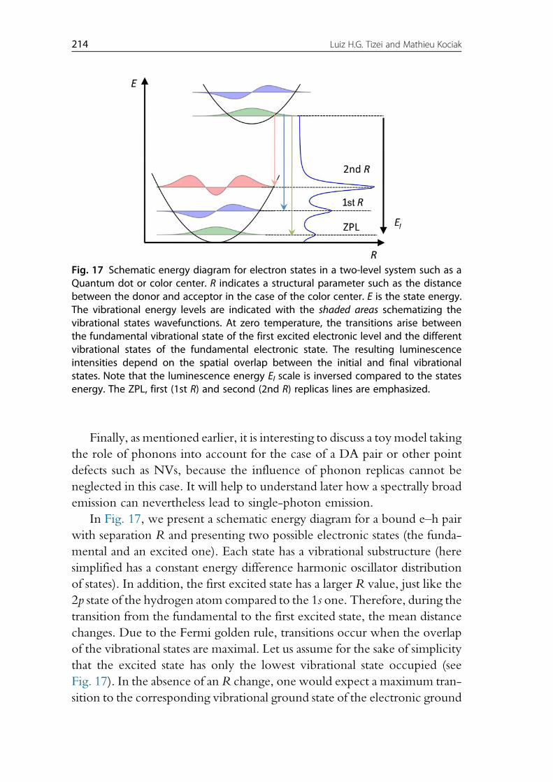
Finally, as mentioned earlier, it is interesting to discuss a toymodel taking
the role of phonons into account for the case of a DA pair or other point
defects such as NVs, because the influence of phonon replicas cannot be
neglected in this case. It will help to understand later how a spectrally broad
emission can nevertheless lead to single-photon emission.
In Fig. 17, we present a schematic energy diagram for a bound e–h pair
with separation R and presenting two possible electronic states (the funda-
mental and an excited one). Each state has a vibrational substructure (here
simplified has a constant energy difference harmonic oscillator distribution
of states). In addition, the first excited state has a larger R value, just like the
2p state of the hydrogen atom compared to the 1s one. Therefore, during the
transition from the fundamental to the first excited state, the mean distance
changes. Due to the Fermi golden rule, transitions occur when the overlap
of the vibrational states are maximal. Let us assume for the sake of simplicity
that the excited state has only the lowest vibrational state occupied (see
Fig. 17). In the absence of anR change, one would expect a maximum tran-
sition to the corresponding vibrational ground state of the electronic ground
Fig. 17 Schematic energy diagram for electron states in a two-level system such as aQuantum dot or color center. R indicates a structural parameter such as the distancebetween the donor and acceptor in the case of the color center. E is the state energy.The vibrational energy levels are indicated with the shaded areas schematizing thevibrational states wavefunctions. At zero temperature, the transitions arise betweenthe fundamental vibrational state of the first excited electronic level and the differentvibrational states of the fundamental electronic state. The resulting luminescenceintensities depend on the spatial overlap between the initial and final vibrationalstates. Note that the luminescence energy El scale is inversed compared to the statesenergy. The ZPL, first (1st R) and second (2nd R) replicas lines are emphasized.
214 Luiz H.G. Tizei and Mathieu Kociak
state, which maximize the overlap integral. In the present case, the overlap is
maximal for another transition (see Fig. 17). The system can therefore emit a
photon while making a transition between two vibrational states with
maximumoverlap and thenwill emit several phonon to reach its fundamental
vibrational state. The excitation then can relax nonradiatively to the mini-
mum vibrational energy state of the fundamental electronic state by emitting
several phonons. This appears as a peak in the spectra and therefore is called a
phonon replica (note the inversed energy scale on the spectrum in the right of
Fig. 17). Exception is made for the higher energy transition involving the
transition from both fundamental vibrational states, called the ZPL as it does
not involved the emission of a phonon.
The corresponding spectrum in Fig. 17 shows the effect of phonon rep-
licas. Contrary to what we would expect from a TLS such as a DAP pair,
the spectrum becomes very large, with all the replicas potentially over-
lapping and which eventually lead to broad bands (Robins, Cook,
Farabaugh, & Feldman, 1989). How can single-photon emission happen
in that conditions that naively has been defined as arising from the transition
from only one pair of state at a time? The contradiction is only apparent.
At any time, whatever excited and fundamental substates are considered,
the states are populated by at most one e–h pair, at least under a moderate
excitation. Even if the energy of the emitted photon is not necessarily the
same at any time, there is always at most one photon in the photon beam,
and SPE can therefore be measured.
5. SINGLE-PHOTON DETECTION IN THE ELECTRONMICROSCOPE
Having described some key points of the interaction between elec-
trons and mater and also general CL experiments, in this section we discuss
some experimental results demonstrating the detection of single-photon
sources (SPE) using a fast electron beam as the excitation source. As
described in previous sections, laser beams in confocal optical microscopes
are typically used for SPE detection. Our motivation to start using electrons
is their reduced wavelength (3.7 pm at 100 keV kinetic energy), which
allows the realization of nanometer-wide beams even in not too complex
machines. To begin, we will describe the use of the HBT interferometer
described in Section 2.2.1 to identify neutral nitrogen vacancy (NV0) centers
in diamond nanoparticles.
215Quantum Nanooptics in the Electron Microscope
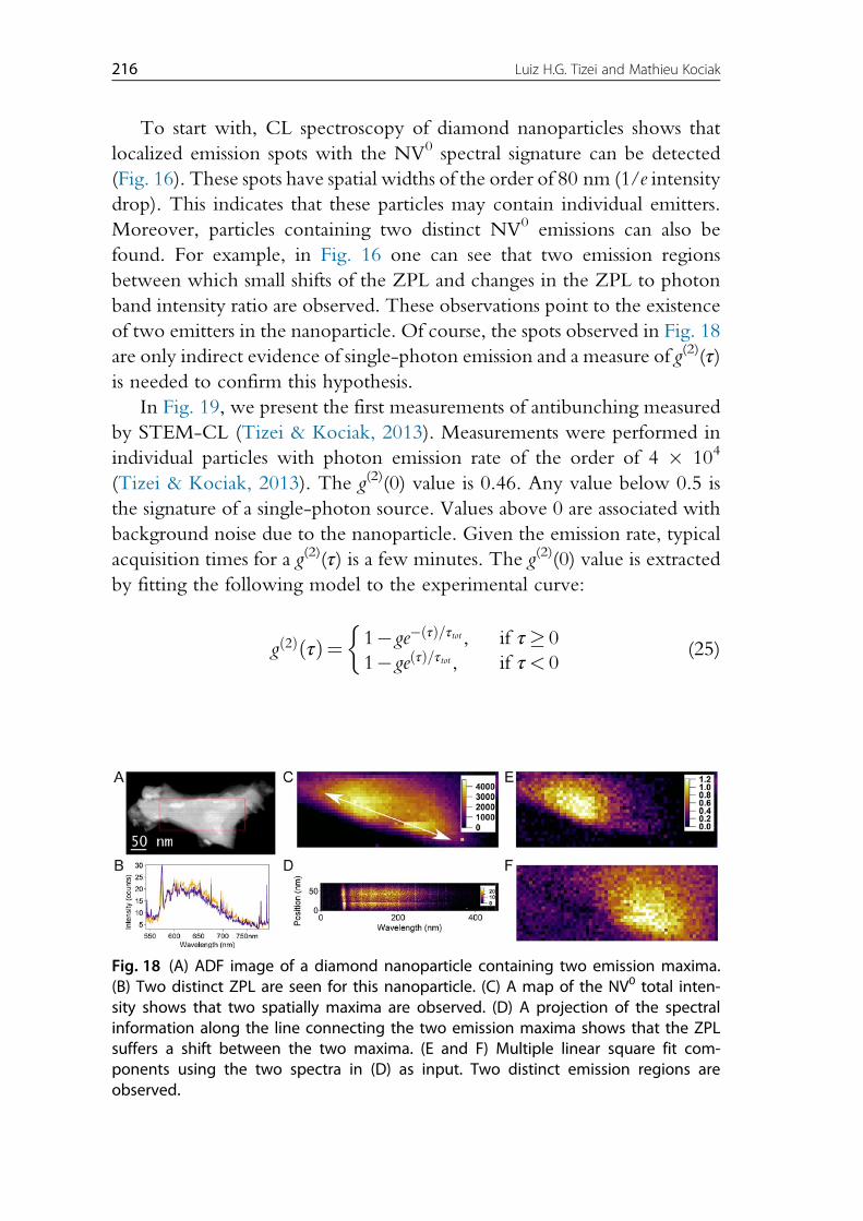
To start with, CL spectroscopy of diamond nanoparticles shows that
localized emission spots with the NV0 spectral signature can be detected
(Fig. 16). These spots have spatial widths of the order of 80 nm (1/e intensity
drop). This indicates that these particles may contain individual emitters.
Moreover, particles containing two distinct NV0 emissions can also be
found. For example, in Fig. 16 one can see that two emission regions
between which small shifts of the ZPL and changes in the ZPL to photon
band intensity ratio are observed. These observations point to the existence
of two emitters in the nanoparticle. Of course, the spots observed in Fig. 18
are only indirect evidence of single-photon emission and a measure of g(2)(τ)is needed to confirm this hypothesis.
In Fig. 19, we present the first measurements of antibunching measured
by STEM-CL (Tizei & Kociak, 2013). Measurements were performed in
individual particles with photon emission rate of the order of 4 & 104
(Tizei & Kociak, 2013). The g(2)(0) value is 0.46. Any value below 0.5 is
the signature of a single-photon source. Values above 0 are associated with
background noise due to the nanoparticle. Given the emission rate, typical
acquisition times for a g(2)(τ) is a few minutes. The g(2)(0) value is extracted
by fitting the following model to the experimental curve:
gð2ÞðτÞ¼ 1% ge%ðτÞ=τtot , if τ$ 01% geðτÞ=τtot , if τ< 0
!(25)
Fig. 18 (A) ADF image of a diamond nanoparticle containing two emission maxima.(B) Two distinct ZPL are seen for this nanoparticle. (C) A map of the NV0 total inten-sity shows that two spatially maxima are observed. (D) A projection of the spectralinformation along the line connecting the two emission maxima shows that the ZPLsuffers a shift between the two maxima. (E and F) Multiple linear square fit com-ponents using the two spectra in (D) as input. Two distinct emission regions areobserved.
216 Luiz H.G. Tizei and Mathieu Kociak
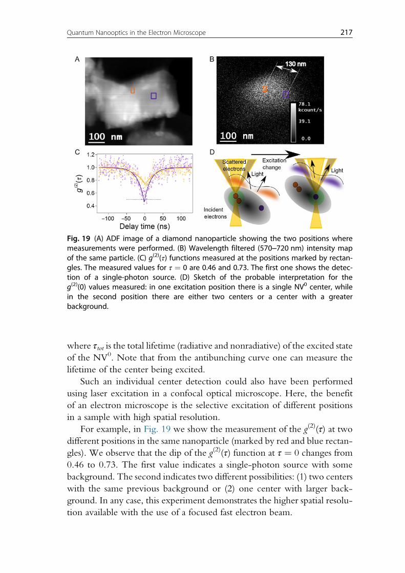
where τtot is the total lifetime (radiative and nonradiative) of the excited state
of the NV0. Note that from the antibunching curve one can measure the
lifetime of the center being excited.
Such an individual center detection could also have been performed
using laser excitation in a confocal optical microscope. Here, the benefit
of an electron microscope is the selective excitation of different positions
in a sample with high spatial resolution.
For example, in Fig. 19 we show the measurement of the g(2)(τ) at twodifferent positions in the same nanoparticle (marked by red and blue rectan-
gles). We observe that the dip of the g(2)(τ) function at τ ¼ 0 changes from
0.46 to 0.73. The first value indicates a single-photon source with some
background. The second indicates two different possibilities: (1) two centers
with the same previous background or (2) one center with larger back-
ground. In any case, this experiment demonstrates the higher spatial resolu-
tion available with the use of a focused fast electron beam.
Fig. 19 (A) ADF image of a diamond nanoparticle showing the two positions wheremeasurements were performed. (B) Wavelength filtered (570–720 nm) intensity mapof the same particle. (C) g(2)(τ) functions measured at the positions marked by rectan-gles. The measured values for τ ¼ 0 are 0.46 and 0.73. The first one shows the detec-tion of a single-photon source. (D) Sketch of the probable interpretation for theg(2)(0) values measured: in one excitation position there is a single NV0 center, whilein the second position there are either two centers or a center with a greaterbackground.
217Quantum Nanooptics in the Electron Microscope
The two experiments described as examples demonstrate the possibility
to detect single-photon sources at high spatial resolution using a focused
beam of fast electrons.
5.1 Background Subtraction in Experiments With ElectronExcitation
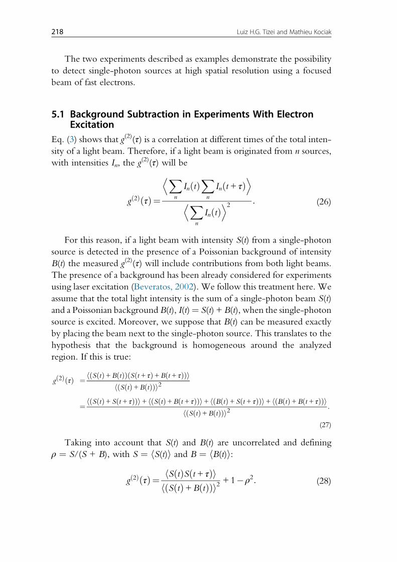
Eq. (3) shows that g(2)(τ) is a correlation at different times of the total inten-
sity of a light beam. Therefore, if a light beam is originated from n sources,
with intensities In, the g(2)(τ) will be
gð2ÞðτÞ¼
DX
n
InðtÞX
n
Inðt + τÞE
DX
n
InðtÞE2 : (26)
For this reason, if a light beam with intensity S(t) from a single-photon
source is detected in the presence of a Poissonian background of intensity
B(t) the measured g(2)(τ) will include contributions from both light beams.
The presence of a background has been already considered for experiments
using laser excitation (Beveratos, 2002). We follow this treatment here. We
assume that the total light intensity is the sum of a single-photon beam S(t)
and a Poissonian background B(t), I(t)¼ S(t) + B(t), when the single-photon
source is excited. Moreover, we suppose that B(t) can be measured exactly
by placing the beam next to the single-photon source. This translates to the
hypothesis that the background is homogeneous around the analyzed
region. If this is true:
gð2ÞðτÞ ¼ hðSðtÞ+BðtÞÞðSðt+ τÞ+Bðt+ τÞÞihðSðtÞ+BðtÞÞi2
¼ hðSðtÞ+ Sðt+ τÞÞi+ hðSðtÞ+Bðt+ τÞÞi+ hðBðtÞ+ Sðt+ τÞÞi+ hðBðtÞ+Bðt+ τÞÞihðSðtÞ+BðtÞÞi2
:
(27)
Taking into account that S(t) and B(t) are uncorrelated and defining
ρ ¼ S/(S + B), with S ¼ hS(t)i and B ¼ hB(t)i:
gð2ÞðτÞ¼ hSðtÞSðt+ τÞihðSðtÞ+BðtÞÞi2
+ 1%ρ2: (28)
218 Luiz H.G. Tizei and Mathieu Kociak
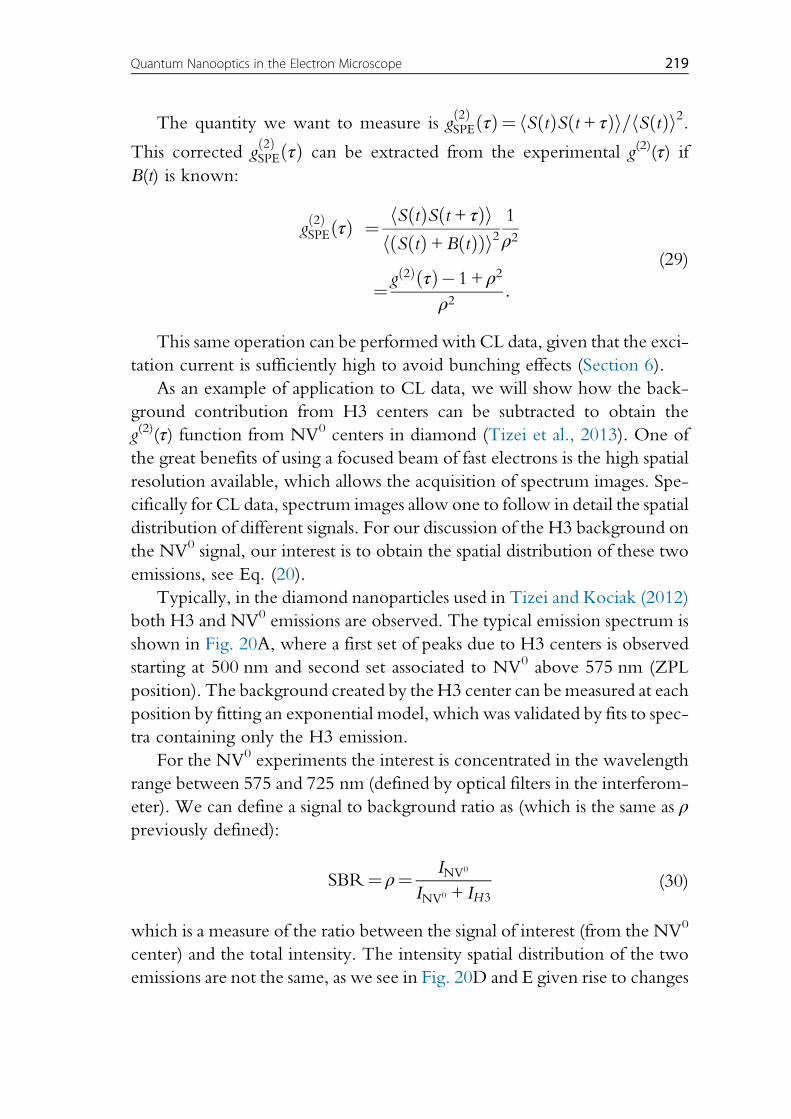
The quantity we want to measure is gð2ÞSPEðτÞ¼ hSðtÞSðt+ τÞi=hSðtÞi2.
This corrected gð2ÞSPEðτÞ can be extracted from the experimental g(2)(τ) if
B(t) is known:
gð2ÞSPEðτÞ ¼ hSðtÞSðt+ τÞi
hðSðtÞ+BðtÞÞi21
ρ2
¼ gð2ÞðτÞ%1+ ρ2
ρ2:
(29)
This same operation can be performed with CL data, given that the exci-
tation current is sufficiently high to avoid bunching effects (Section 6).
As an example of application to CL data, we will show how the back-
ground contribution from H3 centers can be subtracted to obtain the
g(2)(τ) function from NV0 centers in diamond (Tizei et al., 2013). One of
the great benefits of using a focused beam of fast electrons is the high spatial
resolution available, which allows the acquisition of spectrum images. Spe-
cifically for CL data, spectrum images allow one to follow in detail the spatial
distribution of different signals. For our discussion of the H3 background on
the NV0 signal, our interest is to obtain the spatial distribution of these two
emissions, see Eq. (20).
Typically, in the diamond nanoparticles used in Tizei and Kociak (2012)
both H3 and NV0 emissions are observed. The typical emission spectrum is
shown in Fig. 20A, where a first set of peaks due to H3 centers is observed
starting at 500 nm and second set associated to NV0 above 575 nm (ZPL
position). The background created by theH3 center can bemeasured at each
position by fitting an exponential model, which was validated by fits to spec-
tra containing only the H3 emission.
For the NV0 experiments the interest is concentrated in the wavelength
range between 575 and 725 nm (defined by optical filters in the interferom-
eter). We can define a signal to background ratio as (which is the same as ρpreviously defined):
SBR¼ ρ¼ INV0
INV0 + IH3(30)
which is a measure of the ratio between the signal of interest (from the NV0
center) and the total intensity. The intensity spatial distribution of the two
emissions are not the same, as we see in Fig. 20D and E given rise to changes
219Quantum Nanooptics in the Electron Microscope
in the SBR value. The NV0 emission appears mostly concentrated in one
spot in the nanoparticle.
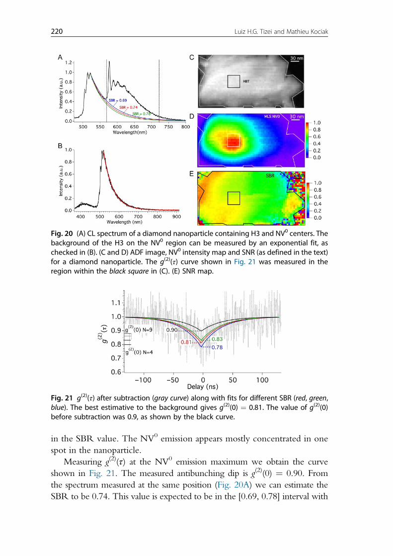
Measuring g(2)(τ) at the NV0 emission maximum we obtain the curve
shown in Fig. 21. The measured antibunching dip is g(2)(0) ¼ 0.90. From
the spectrum measured at the same position (Fig. 20A) we can estimate the
SBR to be 0.74. This value is expected to be in the [0.69, 0.78] interval with
Fig. 20 (A) CL spectrum of a diamond nanoparticle containing H3 and NV0 centers. Thebackground of the H3 on the NV0 region can be measured by an exponential fit, aschecked in (B). (C and D) ADF image, NV0 intensity map and SNR (as defined in the text)for a diamond nanoparticle. The g(2)(τ) curve shown in Fig. 21 was measured in theregion within the black square in (C). (E) SNR map.
Fig. 21 g(2)(τ) after subtraction (gray curve) along with fits for different SBR (red, green,blue). The best estimative to the background gives g(2)(0) ¼ 0.81. The value of g(2)(0)before subtraction was 0.9, as shown by the black curve.
220 Luiz H.G. Tizei and Mathieu Kociak
high confidence. From these values, using Eq. (29), we can see that the actual
g(2)(0) value should be 0.81 and within the interval of confidence [0.78, 0.83].
Before continuing with another application of CL-STEM toward the
detection of single-photon source, we should stress the high spatial resolu-
tion available in experiments using a focused electron probe allows for an
increased SBR, as a smaller volume of the material is excited. Moreover,
the spectrum image capabilities permit the determination of the background
intensity with greater accuracy.
Finally, due to the physics of the electron matter interaction bunching of
light may be observed, as described in Section 6. This introduces possible
errors in the background subtraction procedure. To avoid this problem,
CL-STEM experiment should be performed at sufficiently high current,
as described in Section 6.
5.2 Single-Photons From hBN FlakesOne of the main interests of using fast electrons is the broadband character-
istics of the excitation mechanism. This is true for different reasons,
depending if the excitation is coherent or incoherent (Kociak & Zagonel,
2017). For the coherent mechanism, such as for plasmons, the electro-
magnetic field of the electron directly creates the excitation. As this
field spans a large frequencies range, broadband excitation is possible
(Kociak & Zagonel, 2017). For incoherent mechanism, such as electron–hole pairs creation in semiconductors, the reason is subtler. Typically, a bulk
plasmon is excited by the fast electron beam, which then decays into
electron–hole pairs above the band gap of the material with a given distri-
bution in energy. These pairs will decay toward the band gap and they may
create excitation at different energy levels (for example, different point
defects at distinct energies). This leads again to a broadband emission exci-
tation, as previously described.
In many cases, this broadband excitation can be quite helpful. It allows
one to search a large spectral range in one experiment. Moreover, as it
extends into the ultraviolet range, it allows for experiments which may
be complicated with optics (either because lasers are technologically com-
plicated or inexistent or because of light absorption in the UV range).
New single-photon sources are actively sought for due to possible
applications such as quantum computing and quantum metrology. In the
past, most known single-photon sources were point defects in bulk
matrices (NV in diamond) or confined semiconductors, such as GaN
221Quantum Nanooptics in the Electron Microscope
(Holmes, Choi, Kako, Arita, & Arakawa, 2014; Kako et al., 2006) or InAs
(Moreau et al., 2001). Recently, there have been many reports of single-
photon sources observed in layered materials, such as WSe2 (Koperski
et al., 2015) and hBN (Bourrellier et al., 2016; Tran, Bray, Ford,
Toth, & Aharonovich, 2016).
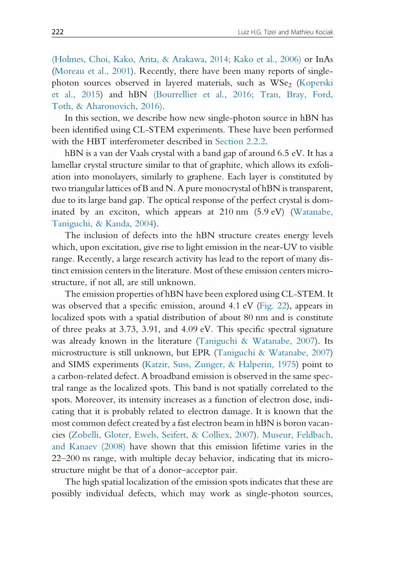
In this section, we describe how new single-photon source in hBN has
been identified using CL-STEM experiments. These have been performed
with the HBT interferometer described in Section 2.2.2.
hBN is a van der Vaals crystal with a band gap of around 6.5 eV. It has a
lamellar crystal structure similar to that of graphite, which allows its exfoli-
ation into monolayers, similarly to graphene. Each layer is constituted by
two triangular lattices of B andN. A pure monocrystal of hBN is transparent,
due to its large band gap. The optical response of the perfect crystal is dom-
inated by an exciton, which appears at 210 nm (5.9 eV) (Watanabe,
Taniguchi, & Kanda, 2004).
The inclusion of defects into the hBN structure creates energy levels
which, upon excitation, give rise to light emission in the near-UV to visible
range. Recently, a large research activity has lead to the report of many dis-
tinct emission centers in the literature.Most of these emission centers micro-
structure, if not all, are still unknown.
The emission properties of hBN have been explored using CL-STEM. It
was observed that a specific emission, around 4.1 eV (Fig. 22), appears in
localized spots with a spatial distribution of about 80 nm and is constitute
of three peaks at 3.73, 3.91, and 4.09 eV. This specific spectral signature
was already known in the literature (Taniguchi & Watanabe, 2007). Its
microstructure is still unknown, but EPR (Taniguchi & Watanabe, 2007)
and SIMS experiments (Katzir, Suss, Zunger, & Halperin, 1975) point to
a carbon-related defect. A broadband emission is observed in the same spec-
tral range as the localized spots. This band is not spatially correlated to the
spots. Moreover, its intensity increases as a function of electron dose, indi-
cating that it is probably related to electron damage. It is known that the
most common defect created by a fast electron beam in hBN is boron vacan-
cies (Zobelli, Gloter, Ewels, Seifert, & Colliex, 2007). Museur, Feldbach,
and Kanaev (2008) have shown that this emission lifetime varies in the
22–200 ns range, with multiple decay behavior, indicating that its micro-
structure might be that of a donor–acceptor pair.The high spatial localization of the emission spots indicates that these are
possibly individual defects, which may work as single-photon sources,
222 Luiz H.G. Tizei and Mathieu Kociak
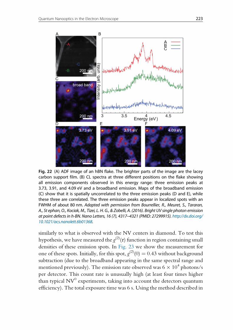
similarly to what is observed with the NV centers in diamond. To test this
hypothesis, we have measured the g(2)(τ) function in region containing small
densities of these emission spots. In Fig. 23 we show the measurement for
one of these spots. Initially, for this spot, g(2)(0) ¼ 0.43 without background
subtraction (due to the broadband appearing in the same spectral range and
mentioned previously). The emission rate observed was 6& 104 photons/s
per detector. This count rate is unusually high (at least four times higher
than typical NV0 experiments, taking into account the detectors quantum
efficiency). The total exposure time was 6 s. Using the method described in
Fig. 22 (A) ADF image of an hBN flake. The brighter parts of the image are the laceycarbon support film. (B) CL spectra at three different positions on the flake showingall emission components observed in this energy range: three emission peaks at3.73, 3.91, and 4.09 eV and a broadband emission. Maps of the broadband emission(C) show that it is spatially uncorrelated to the three emission peaks (D and E), whilethese three are correlated. The three emission peaks appear in localized spots with anFWHM of about 80 nm. Adapted with permission from Bourrellier, R., Meuret, S., Tararan,A., St ephan, O., Kociak, M., Tizei, L. H. G., & Zobelli, A. (2016). Bright UV single photon emissionat point defects in h-BN. Nano Letters, 16 (7), 4317–4321 (PMID: 27299915). http://dx.doi.org/10.1021/acs.nanolett.6b01368.
223Quantum Nanooptics in the Electron Microscope
Section 5.1 we have subtracted the broadband contribution obtaining
g(2)(0) ¼ 0.2. Both values are below the 0.5 threshold, demonstrating a
single-photon source.
A second measurement was performed on the same emission spot. The
spectrum observed shows the previously observed three peaks with similar
intensity. However, the broadband shows a higher emission intensity
(Fig. 23D). With the higher background we measured g(2)(0) ¼ 0.58.
However, once again, after background subtraction g(2)(0) ¼ 0.2 (Fig. 23F).
These results give support to the fact that the 3-peak emission stems from a
single-photon source, possibly a point defect.
The detection of a new single-photon source using CL-STEM experi-
ments demonstrates that standard quantum optics experiments may benefit
from the high spatial resolution and broadband excitation available in elec-
tron microscopes.
1.2
1.0
0.8
0.6
0.4
0.2
0.0
1.3
0.58
0.20.00.20.40.60.81.01.21.41.61.8
1.2
1.0
0.8
0.6
0.4
g(2) (t
)g(2
) (t
)
–40 –20 0 20 40Delay (ns)
–40 –20 0 20 40Delay (ns)
0.2
Corrected g
(2) (t)C
orrected g(2) (t)
0.430.2
0.0
1.3
0.00.20.40.60.81.01.21.41.6
Energy (eV)3.0 3.5 4.0 4.5 5.0
Energy (eV)3.0 3.5 4.0 4.5 5.0
Cou
nts
Cou
nts
A C E
B D F
500 nm
500 nm
Fig. 23 (A) ADF image of an hBN flake. (B) Intensity map filtered around the energy ofthe 4.1 eV center. (C) CL spectrum when the spot was excited. (D) CL spectrum afterelectron irradiation of the same spot. (E) g(2)(τ) function measured while the regionaround the emission spot excited before irradiation. The value of g(2)(0)¼ 0.2, after back-ground subtraction, demonstrates this to be a single-photon source. (F)g(2)(τ) functionmeasured while the region around the emission spot excited after irradiation. Afterbackground subtraction the same g(2)(0) ¼ 0.2 was observed. Adapted with permissionfrom Bourrellier, R., Meuret, S., Tararan, A., St!ephan, O., Kociak, M., Tizei, L. H. G., & Zobelli, A.(2016). Bright UV single photon emission at point defects in h-BN. Nano Letters, 16 (7),4317–4321 (PMID: 27299915). http://dx.doi.org/10.1021/acs.nanolett.6b01368.
224 Luiz H.G. Tizei and Mathieu Kociak
6. LIGHT BUNCHING IN CL
In a first approximation, the physics of excitation creation in semicon-
ductor and wide-band gap materials by fast electron beam is fairly similar to
that of off-resonance laser excitation.ThereforeCL spectral signature is equiv-
alent to that of off-resonance PL (Mahfoud et al., 2013). However, the exact
details of electron–hole pair creation are not the same. In particular, the decay
of bulk plasmons may lead to the creation of more than one electron–holepair, what allows the excitation of different emission centers in finite temporal
windows (centers which will be the source of the light detected in experi-
ments). The impact of this particularity is the topic of this section.
As already described in Section 3, most inelastic scattering events of a fast
electron in matter create a bulk plasmon (Egerton, 1996), which are collec-
tive excitations valence band electrons (Egerton, 1996) and have a typical
energy between 10 and 30 eV in semiconductors. These high energy exci-
tation may decay through different channels, including electron–hole pairswith energy close to the band gap energy. As the band gap energy is inci-
dentally smaller than that of the bulk plasmon (3.5 eV in GaN, for example),
many electron–hole pair may be created upon a single decay. This fact was
already considered in the past, with models predicting different total number
of pairs (Klein, 1968). In any case, the key fact is the creation of more than
one electron–hole pair per bulk plasmon decay (and also electron–material
inelastic scattering).
At this point, it is important to note the typical times involved in the
complete scattering/decay/light emission process. The transit time of a fast
electron (speed a fraction of the speed of light) during which it interacts with
the material is of the order of a few femtoseconds. The created bulk plasmon
will eventually decay, possibly creating electron–hole pairs. The decay pro-cess takes place in time scales of the order of femtoseconds. The electron–hole pairs created will diffuse until their decay, which might occur while
transferring energy to a possible light emission center (such as a NV0 center).
This process occurs in a picosecond time scale. Finally, the excited centers
will decay emitting photons in a time scale dictated by their lifetimes (from
picoseconds to microseconds).
If centers with long lifetimes (compared with the whole excitation process
time) are probed, within a good approximation they can be said to be excited
synchronously by the decay of a bulk plasmon. In this case, the photons emit-
tedwill all exit the sample in a light packet (or bunch) in a timewindowof the
225Quantum Nanooptics in the Electron Microscope
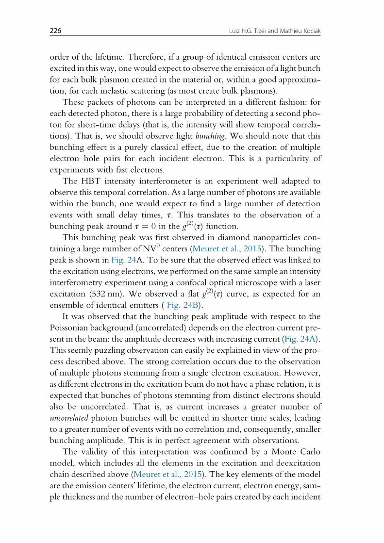
order of the lifetime. Therefore, if a group of identical emission centers are
excited in this way, onewould expect to observe the emission of a light bunch
for each bulk plasmon created in the material or, within a good approxima-
tion, for each inelastic scattering (as most create bulk plasmons).
These packets of photons can be interpreted in a different fashion: for
each detected photon, there is a large probability of detecting a second pho-
ton for short-time delays (that is, the intensity will show temporal correla-
tions). That is, we should observe light bunching. We should note that this
bunching effect is a purely classical effect, due to the creation of multiple
electron–hole pairs for each incident electron. This is a particularity of
experiments with fast electrons.
The HBT intensity interferometer is an experiment well adapted to
observe this temporal correlation. As a large number of photons are available
within the bunch, one would expect to find a large number of detection
events with small delay times, τ. This translates to the observation of a
bunching peak around τ ¼ 0 in the g(2)(τ) function.This bunching peak was first observed in diamond nanoparticles con-
taining a large number of NV0 centers (Meuret et al., 2015). The bunching
peak is shown in Fig. 24A. To be sure that the observed effect was linked to
the excitation using electrons, we performed on the same sample an intensity
interferometry experiment using a confocal optical microscope with a laser
excitation (532 nm). We observed a flat g(2)(τ) curve, as expected for an
ensemble of identical emitters ( Fig. 24B).
It was observed that the bunching peak amplitude with respect to the
Poissonian background (uncorrelated) depends on the electron current pre-
sent in the beam: the amplitude decreases with increasing current (Fig. 24A).
This seemly puzzling observation can easily be explained in view of the pro-
cess described above. The strong correlation occurs due to the observation
of multiple photons stemming from a single electron excitation. However,
as different electrons in the excitation beam do not have a phase relation, it is
expected that bunches of photons stemming from distinct electrons should
also be uncorrelated. That is, as current increases a greater number of
uncorrelated photon bunches will be emitted in shorter time scales, leading
to a greater number of events with no correlation and, consequently, smaller
bunching amplitude. This is in perfect agreement with observations.
The validity of this interpretation was confirmed by a Monte Carlo
model, which includes all the elements in the excitation and deexcitation
chain described above (Meuret et al., 2015). The key elements of the model
are the emission centers’ lifetime, the electron current, electron energy, sam-
ple thickness and the number of electron–hole pairs created by each incident
226 Luiz H.G. Tizei and Mathieu Kociak
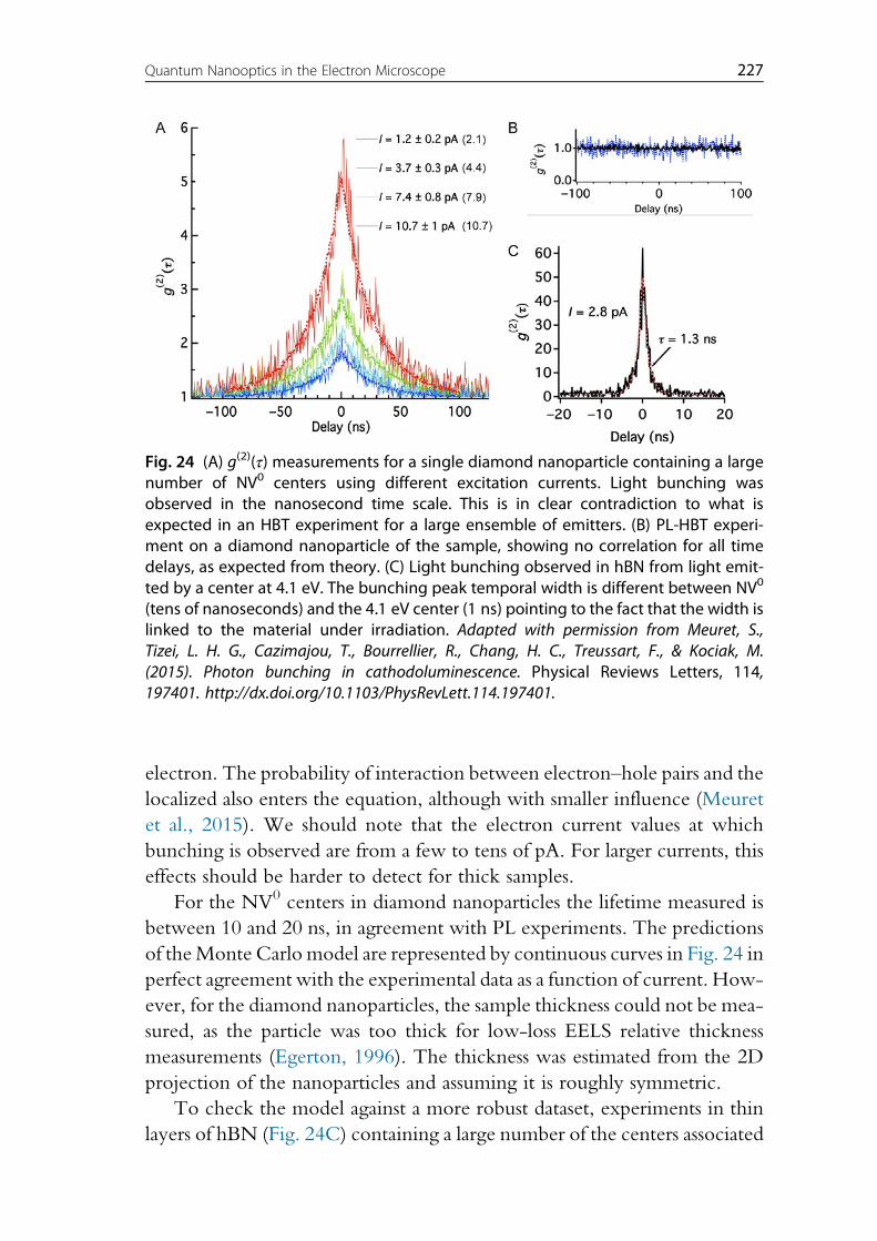
electron. The probability of interaction between electron–hole pairs and thelocalized also enters the equation, although with smaller influence (Meuret
et al., 2015). We should note that the electron current values at which
bunching is observed are from a few to tens of pA. For larger currents, this
effects should be harder to detect for thick samples.
For the NV0 centers in diamond nanoparticles the lifetime measured is
between 10 and 20 ns, in agreement with PL experiments. The predictions
of theMonte Carlo model are represented by continuous curves in Fig. 24 in
perfect agreement with the experimental data as a function of current. How-
ever, for the diamond nanoparticles, the sample thickness could not be mea-
sured, as the particle was too thick for low-loss EELS relative thickness
measurements (Egerton, 1996). The thickness was estimated from the 2D
projection of the nanoparticles and assuming it is roughly symmetric.
To check the model against a more robust dataset, experiments in thin
layers of hBN (Fig. 24C) containing a large number of the centers associated
Fig. 24 (A) g(2)(τ) measurements for a single diamond nanoparticle containing a largenumber of NV0 centers using different excitation currents. Light bunching wasobserved in the nanosecond time scale. This is in clear contradiction to what isexpected in an HBT experiment for a large ensemble of emitters. (B) PL-HBT experi-ment on a diamond nanoparticle of the sample, showing no correlation for all timedelays, as expected from theory. (C) Light bunching observed in hBN from light emit-ted by a center at 4.1 eV. The bunching peak temporal width is different between NV0
(tens of nanoseconds) and the 4.1 eV center (1 ns) pointing to the fact that the width islinked to the material under irradiation. Adapted with permission from Meuret, S.,Tizei, L. H. G., Cazimajou, T., Bourrellier, R., Chang, H. C., Treussart, F., & Kociak, M.(2015). Photon bunching in cathodoluminescence. Physical Reviews Letters, 114,197401. http://dx.doi.org/10.1103/PhysRevLett.114.197401.
227Quantum Nanooptics in the Electron Microscope
with the single-photon source previously described have been performed.
The thickness of the layers was measured using low-loss EELS. Using this
information and the previously described measured quantities, the expected
g(2)(τ) can be calculated, which are in agreement with the measured curves.
These two experiments and the associated mode give support to the
interpretation provided for the observation of bunching in light emitted
from materials excited by fast electrons.
7. LIFETIME MEASUREMENTS AT THE NANOMETERSCALE
An interesting aspect of the light bunching effect described in the pre-
vious section is that if only one type of emitter is excited, its associated life-
time can be measured with high spatial resolution. This is true, because the
decay of the bunching peak at zero time delay can be approximated by an
exponential decay (Meuret et al., 2016, 2015). This can already be seen from
the proposed model and from a comparison between the bunching peaks in
NV0 experiments with literature time-resolved PL (TR-PL) experiments
(Liaugaudas, Davies, Suhling, Khan, & Evans, 2012). We should note that
time-resolved CL experiments also allow lifetime measurements (Merano
et al., 2005). However, a direct comparison between CL and PL is necessary.
Experiments in GaN quantum disks in AlN nanowires comparing these
techniques will be described in the next section.
7.1 GaN Quantum Disks: PL vs CLTo demonstrate the equivalence of CL bunching measurements and TR-PL
to measure lifetimes a series of experiments in AlN nanowires containing
single GaN quantum disks has been performed. The reason to use individual
QDisks is that TR-CL do not provide sufficient spatial resolution to distin-
guish multiple quantum disks inside the same nanowire. These experiments
have been performed using the HBT interferometer described in
Section 2.2.2 for CL experiments and a confocal microscope also with an
HBT interferometer for spatially resolved TR-PL experiments. For the fully
optical experiment the spatial resolution was of the order of 1 μm.
To allow experiments in transmission in the electron microscope and in
a confocal optical microscope, the nanowires were dispersed on Si chips
containing 100 & 100 μm2 holes covered by a 15 nm thick Si3N4 film.
228 Luiz H.G. Tizei and Mathieu Kociak
In principle, the experiments should have been performed in the same nano-
wires, starting with the CL experiments to prevent any electron
beam-induced damage. However, during TR-PL experiments, it has been
realized that the sample would drift by large distances when nanowires on
the thin membrane were excited by the laser beam. This drift was probably
a result of thermal dilatation induced by sample heating.
As a result experiments were performed on two sets of nanowires, both
on the same Si3N4 grid. The lifetime measurements plotted against the
quantum disks emission energy for both techniques are shown in Fig. 25.
As one can see, the data points disperse around a line—due to the QCSE,
showing that both datasets agree statistically. This demonstrates that light
bunching in CL experiments measures the same quantity as TR-PL.
In the next section we will show how the bunching effect can be used to
measure lifetimes with nanometer spatial resolution.
7.2 GaN Quantum Disks: Spatial ResolutionThe lifetime of objects separated by large distances (greater than at least
1 μm) can be measured by all-optical techniques, such as TR-PL. However,
for objects more closely packed, techniques with greater spatial resolution.
One solution is the use of time-resolved cathodoluminescence (TR-CL),
Fig. 25 Lifetime measurements for single GaN QDisks in AlN nanowires using TR-PL(orange diamonds) and bunching in CL (purple circles). The dependence of lifetime withemission energy is the expected one. The statistical agreement betweenmeasurementsshows that bunching in CL indeed measures lifetimes. Adapted with permission fromMeuret, S., Tizei, L. H. G., Auzelle, T., Songmuang, R., Daudin, B., Gayral, B., & Kociak, M.(2016). Lifetime measurements well below the optical diffraction limit. ACS Photonics,3(7), 1157–1163. http://dx.doi.org/10.1021/acsphotonics.6b00212.
229Quantum Nanooptics in the Electron Microscope
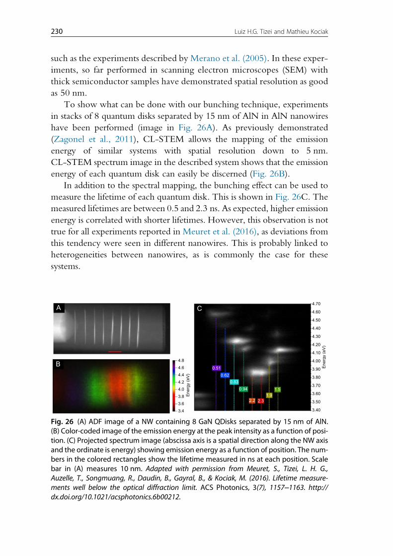
such as the experiments described by Merano et al. (2005). In these exper-
iments, so far performed in scanning electron microscopes (SEM) with
thick semiconductor samples have demonstrated spatial resolution as good
as 50 nm.
To show what can be done with our bunching technique, experiments
in stacks of 8 quantum disks separated by 15 nm of AlN in AlN nanowires
have been performed (image in Fig. 26A). As previously demonstrated
(Zagonel et al., 2011), CL-STEM allows the mapping of the emission
energy of similar systems with spatial resolution down to 5 nm.
CL-STEM spectrum image in the described system shows that the emission
energy of each quantum disk can easily be discerned (Fig. 26B).
In addition to the spectral mapping, the bunching effect can be used to
measure the lifetime of each quantum disk. This is shown in Fig. 26C. The
measured lifetimes are between 0.5 and 2.3 ns. As expected, higher emission
energy is correlated with shorter lifetimes. However, this observation is not
true for all experiments reported in Meuret et al. (2016), as deviations from
this tendency were seen in different nanowires. This is probably linked to
heterogeneities between nanowires, as is commonly the case for these
systems.
4.8
A
B
C4.70
4.60
4.50
4.40
4.30
4.20
4.10
4.00
3.90
3.80
3.70
3.60
3.50
3.40
1.51.9
2.32.2
0.94
0.83
0.62
0.514.6
4.4
4.2
4.0
Ene
rgy
(eV
)
Ene
rgy
(eV
)
3.8
3.6
3.4
Fig. 26 (A) ADF image of a NW containing 8 GaN QDisks separated by 15 nm of AlN.(B) Color-coded image of the emission energy at the peak intensity as a function of posi-tion. (C) Projected spectrum image (abscissa axis is a spatial direction along the NW axisand the ordinate is energy) showing emission energy as a function of position. The num-bers in the colored rectangles show the lifetime measured in ns at each position. Scalebar in (A) measures 10 nm. Adapted with permission from Meuret, S., Tizei, L. H. G.,Auzelle, T., Songmuang, R., Daudin, B., Gayral, B., & Kociak, M. (2016). Lifetime measure-ments well below the optical diffraction limit. ACS Photonics, 3(7), 1157–1163. http://dx.doi.org/10.1021/acsphotonics.6b00212.
230 Luiz H.G. Tizei and Mathieu Kociak
8. PERSPECTIVES
The developments described in this text concern the use of the high
resolution of a free-electron beam in conjunction with the statistical and
quantum properties of light to explore new physics at reduced dimensions.
This is a small contribution in a very active field aimed at the active control
of electron beams (possibly in conjunction with a light beam) to probe new
physical effects. The vast range of new developments, which have large fun-
damental interest by themselves, might be efficiently coupled to experiments
such as those described here to dive deeper in quantum nanooptics.
For example, pulsed guns technology, should they be applied to SEM (Fu
et al., 2014; Grundmann, Christen, Bimberg, Fischer-Colbrie, & Hull, 1989;
Merano et al., 2005) or to TEM (Barwick, Flannigan, & Zewail, 2009) are
progressing quickly, with typical pulses times duration ranging from
sub-picoseconds to nanoseconds. There is, therefore, room for applying
the power of PL techniques relying on time resolution to CL (Meuret
et al., 2017). In addition, it has recently been demonstrated that quantumopti-
cal experiments with the free-electron beam of a TEM could be performed (Feist
et al., 2015). In other words, it is possible to evidence the quantum nature of
the free-electron beam through the creation of quantum superpositions of
free-electron states. Combining the full quantum properties of the incoming
electron, the material of interest and the electromagnetic field is a totally new
and exciting field of investigation. Finally, the wave behavior of the
free-electron beam is at the basis of many imaging techniques in EM (high
resolution, holography and all their derivatives). However, only very recently
it has been possible to manipulate the phase of the free electrons with the flex-
ibility that is ordinary in optical physics. This has first been demonstrated to
form exotic forms of waves such as vortex electron beams (Verbeeck, Tian, &
Schattschneider, 2010). Phase-shaped beams can be now created with theo-
retically any symmetry. Symmetry engineering has been proved to be
extremely efficient to study surface plasmons symmetry (Guzzinati et al.,
2016) in the visible range. We can guess that such symmetry engineering
would be quite useful to the study of quantum nanooptical systems.
ACKNOWLEDGMENTSThe authors would like to express gratitude to all colleagues for fundamental contributionswhich were key to the developments described here and discussions over the years that
greatly helped building the concepts discussed in this text. Specially, we would like to
231Quantum Nanooptics in the Electron Microscope
thank Sophie Meuret for the great collaboration over the years as well as Francois Treussartfor his great insights into diamond photo-physics and the continual collaboration. We wouldlike to thanks also Romain Bourrelier, Alberto Zobelli, Anna Tararan, Marcel Tenc!e,Jean-Denis Blazit, Bruno Daudin, Bruno Gayral, No!emie Bonnet, and Henrikas Svidrasfor their contributions and collaboration.
REFERENCESBarjon, J., Tillocher, T., Habka, N., Brinza, O., Achard, J., Issaoui, R.,…Bergonzo, P.
(2011). Boron acceptor concentration in diamond from excitonic recombination inten-sities. Physical Review B, 83(7), 073201.
Barwick, B., Flannigan, D. J., & Zewail, A. H. (2009). Photon-induced near-field electronmicroscopy. Nature, 462(7275), 902–906. http://dx.doi.org/10.1038/nature08662.
Beveratos, A. (2002). R!ealisation exp!erimental d’une source de photons uniques par fluorescence decentres color!es dans le diamant. Application à la cryptographie quantique. (PhD thesis).Universit!e Paris XI.
Beveratos, A., Brouri, R., Poizat, J., & Grangier, P. (2001). Bunching and anti bunchingfrom single NV color centers in diamond. In P. Tombesi & O. Hirota (Eds.), Quantumcommunication, computing, and measurement 3. New York: Springer.
Bourrellier, R., Meuret, S., Tararan, A., St!ephan, O., Kociak, M., Tizei, L. H. G., &Zobelli, A. (2016). Bright UV single photon emission at point defects in h-BN. NanoLetters, 16(7), 4317–4321. (PMID: 27299915). http://dx.doi.org/10.1021/acs.nanolett.6b01368.
Burton, N., Steeds, J., Meaden, G., Shreter, Y., & Butler, J. (1995). Strain and microstructurevariation in grains of CVD diamond film. Diamond and Related Materials, 4(10),1222–1234. http://dx.doi.org/10.1016/0925-9635(95)00300-2.
Das, P., Chini, T. K., & Pond, J. (2012). Probing higher order surface plasmon modes onindividual truncated tetrahedral gold nanoparticle using cathodoluminescence imagingand spectroscopy combined with FDTD simulations. Journal of Physical Chemistry C,116(29), 15610–15619. http://dx.doi.org/10.1021/jp3047533.
Doherty, M.W., Manson, N. B., Delaney, P., Jelezko, F., Wrachtrup, J., & Hollenberg, L. C.(2013). The nitrogen-vacancy colour centre in diamond. Physics Reports, 528(1), 1–45.http://www.sciencedirect.com/science/article/pii/S0370157313000562. http://dx.doi.org/10.1016/j.physrep.2013.02.001.
Drouin, D., Couture, A. R., Joly, D., Tastet, X., Aimez, V., & Gauvin, R. (2007). CASINOV2.42: A fast and easy-to-use modeling tool for scanning electron microscopy andmicroanalysis users. Scanning, 29(3), 92–101.
Edwards, P. R., & Martin, R. W. (2011). Cathodoluminescence nano-characterization ofsemiconductors. Semiconductor Science and Technology, 26(6), 064005.
Egerton, R. (1996). EELS in the electron microscope. Berlin: Springer.Feist, A., Echternkamp, K. E., Schauss, J., Yalunin, S. V., Schaefer, S., & Ropers, C. (2015).
Quantum coherent optical phase modulation in an ultrafast transmission electron micro-scope. Nature, 521(7551), 200–203. http://dx.doi.org/10.1038/nature14463.
Fox, M. (2006). Quantum optics: An introduction. Oxford: Oxford University Press.Fox, M. (2010). In Optical properties of solids (Vol. 3). Oxford: Oxford University Press.Fu, X., Jacopin, G., Shahmohammadi, M., Liu, R., Benameur,M., Ganiere, J.-D.,…Yu, D.
(2014). Exciton drift in semiconductors under uniform strain gradients: Application tobent ZnO microwires. ACS Nano, 8(4), 3412–3420. http://dx.doi.org/10.1021/nn4062353.
Gruber, A., Dr€abenstedt, A., Tietz, C., Fleury, L., Wrachtrup, J., & von Borczyskowski, C.(1997). Scanning confocal optical microscopy andmagnetic resonance on single defect cen-ters. Science, 276(5321), 2012–2014. http://dx.doi.org/10.1126/science.276.5321.2012.
232 Luiz H.G. Tizei and Mathieu Kociak
Grundmann, M., Christen, J., Bimberg, D., Fischer-Colbrie, A., & Hull, R. (1989). Misfitdislocations in pseudomorphic In0.23Ga0.77As/GaAs quantum wells: Influence on life-time and diffusion of excess excitons. Journal of Applied Physics, 66(5), 2214.
Guzzinati, G., B!ech!e, A., Lourenco-Martins, H., Martin, J., Kociak, M., & Verbeeck, J.(2016). Probing the symmetry and phase of localised surface plasmon resonances with modified elec-tron probes. (arXiv preprint arXiv:1608.07449).
Hanbury, B. R., & Twiss, R. Q. (1956). Correlation between photons in two coherentbeams of light. Nature, 178, 1046.
Holmes, M. J., Choi, K., Kako, S., Arita, M., & Arakawa, Y. (2014). Room-temperaturetriggered single photon emission from a III-nitride site-controlled nanowire quantumdot. Nano Letters, 14(2), 982–986. http://dx.doi.org/10.1021/nl404400d.
Jelezko, F., &Wrachtrup, J. (2006). Single defect centres in diamond: A review. Physica StatusSolidi A: Applications and Material Science, 203(13), 3207–3225. http://dx.doi.org/10.1002/pssa.200671403.
Kako, S., Santor, C., Hoshino, K., G€otzinger, S., Yamamoto, Y., & Arakawa, Y. (2006).A gallium nitride single-photon source operating at 200 K.Nature Materials, 5, 887–892.
Kalliakos, S., Bretagnon, T., Lefebvre, P., Taliercio, T., Gil, B., Grandjean, N.,…Massies, J.(2004). Photoluminescence energy and linewidth in GaN/AlN stackings of quantum dotplanes. Journal of Applied Physics, 96(1), 180–185. http://dx.doi.org/10.1063/1.1753085.
Katzir, A., Suss, J. T., Zunger, A., & Halperin, A. (1975). Point defects in hexagonal boronnitride. I. EPR, thermoluminescence, and thermally-stimulated-current measurements.Physical Review B, 11, 2370–2377. http://dx.doi.org/10.1103/PhysRevB.11.2370.
Kimble, H. J., Dagenais, M., & Mandel, L. (1977). Photon antibunching in resonance fluo-rescence. Physical Reviews Letters, 39, 691–695.
Klein, C. A. (1968). Bandgap dependence and related features of radiation ionization energiesin semiconductors. Journal of Applied Physics, 39(4), 2029–2038.
Kociak, M., St!ephan, O., Walls, M., & Colliex, C. (2011). Spatially resolved EELS: Thespectrum-imaging technique and its applications. New York: Springer, 163 (chapter 4).
Kociak, M., & Zagonel, L. F. (2017). Cathodoluminescence in the scanning transmissionelectron microscope. Ultramicroscopy, 174, 50–69.
Koperski, M., Nogajewski, K., Arora, A., Cherkez, V., Mallet, P., Veuillen, J. Y.,…Potemski, M. (2015). Single photon emitters in exfoliatedWSe2 structures.Nature Nano-technology, 10, 503–506.
Lamb, W. E. (1995). Anti-photon. Applied Physics B, 60(2), 77–84.Lefebvre, J., Homma, Y., & Finnie, P. (2003). Bright band gap photoluminescence from
unprocessed single-walled carbon nanotubes. Physical Review Letters, 90(21), 217401.Lefebvre, P., & Gayral, B. (2008). Optical properties of GaN/AlN quantum dots. Comptes
Rendus Physique, 9(8), 816–829. http://dx.doi.org/10.1016/j.crhy.2008.10.008.Liaugaudas, G., Davies, G., Suhling, K., Khan, R. U. A., & Evans, D. J. F. (2012). Lumi-
nescence lifetimes of neutral nitrogen-vacancy centres in synthetic diamond containingnitrogen. Journal of Physics: Condensed Matter, 24(43), 435503. http://stacks.iop.org/0953-8984/24/i¼43/a¼435503.
Losquin, A., & Lummen, T. T. (2017). Electron microscopy methods for space-, energy-,and time-resolved plasmonics. Frontiers of Physics, 12(1), 127301.
Losquin, A., Zagonel, L. F., Myroshnychenko, V., Rodrıguez-Gonzalez, B., Tenc!e, M.,Scarabelli, L.,…Kociak, M. (2015). Unveiling nanometer scale extinction and scatteringphenomena through combined electron energy loss spectroscopy and catho-doluminescence measurements. Nano Letters, 15(2), 1229–1237 (PMID: 25603194).
Loudon, R. (2000). The quantum theory of light. Oxford: Oxford University Press.Mahfoud, Z., Dijksman, A. T., Javaux, C., Bassoul, P., Baudrion, A.-L., Plain, J.,…
Kociak, M. (2013). Cathodoluminescence in a scanning transmission electron micro-scope: A nanometer-scale counterpart of photoluminescence for the study of II–VI
233Quantum Nanooptics in the Electron Microscope
quantum dots. Journal of Physical Chemistry Letters, 4, 4090–4094. http://www.stem.lps.u-psud.fr/sites/default/files/Mahfoud2013_7.pdf. http://dx.doi.org/10.1021/jz402233x.
Merano, M., Sonderegger, S., Crottini, A., Collin, S., Renucci, P., Pelucchi, E.,…Ganiere1, J.-D. (2005). Probing carrier dynamics in nanostructures by picosecond cat-hodoluminescence. Nature, 438, 479–482.
Meuret, S., et al. (2017). (in preparation).Meuret, S., Tizei, L. H. G., Auzelle, T., Songmuang, R., Daudin, B., Gayral, B., &
Kociak, M. (2016). Lifetime measurements well below the optical diffraction limit.ACS Photonics, 3(7), 1157–1163. http://dx.doi.org/10.1021/acsphotonics.6b00212.
Meuret, S., Tizei, L. H. G., Cazimajou, T., Bourrellier, R., Chang, H. C., Treussart, F., &Kociak, M. (2015). Photon bunching in cathodoluminescence. Physical Reviews Letters,114, 197401. http://dx.doi.org/10.1103/PhysRevLett.114.197401.
Miller, D. A. B., Chemla, D. S., Damen, T. C., Gossard, A. C., Wiegmann, W.,Wood, T. H., & Burrus, C. A. (1984). Band-edge electroabsorption in quantum wellstructures—The quantum-confined stark-effect. Physical Review Letters, 53(22),2173–2176.
Moreau, E., Robert, I., Gerard, J. M., Abram, I., Manin, L., & Thierry-Vieg, V. (2001).Single-mode solid-state single photon source based on isolated quantum dots in pillarmicrocavities. Applied Physics Letters, 79, 2865–2867.
Museur, L., Feldbach, E., & Kanaev, A. (2008). Defect-related photoluminescence of hex-agonal boron nitride. Physical Review B, 78, 155204. http://dx.doi.org/10.1103/PhysRevB.78.155204.
Peter, Y., & Cardona, M. (2010). Fundamentals of semiconductors: Physics and materials properties.Berlin: Springer Science & Business Media.
Robins, L. H., Cook, L. P., Farabaugh, E. N., & Feldman, A. (1989). Cathodoluminescenceof defects in diamond films and particles grown by hot-filament chemical-vapor depo-sition. Physical Review B, 39(18), 13367–13377. http://dx.doi.org/10.1103/PhysRevB.39.13367.
Sieber, B. (2016). Cathodoluminescence principes physiques et systes de d!ection. Techniques del’ing!enieur Analyses de surface et de mat!eriaux. http://www.techniques-ingenieur.fr/base-documentaire/mesures-analyses-th1/analyses-de-surface-et-de-materiaux-42383210/cathodoluminescence-p3792/(base documentaire: TIB383DUO. (ref. article: p3792)).
Taniguchi,T.,&Watanabe,K. (2007).Synthesisofhigh-purityboronnitride singlecrystalsunderhigh pressure by using Ba–BN solvent. Journal of Crystal Growth, 303(2), 525–529.http://www.sciencedirect.com/science/article/pii/S0022024807000486. http://dx.doi.org/10.1016/j.jcrysgro.2006.12.061.
Tanuma, S., Powell, C. J., & Penn, D. R. (2011). Calculations of electron inelastic mean freepaths. IX. Data for 41 elemental solids over the 50 eV to 30 keV range. Surface and Inter-face Analysis, 43(3), 689–713.
Tizei, L. H. G., & Kociak, M. (2012). Spectrally and spatially resolved cathodoluminescenceof nanodiamonds: Local variations of the NV(0) emission properties. Nanotechnology,23(17), 175702. http://www.ncbi.nlm.nih.gov/pubmed/22481219. http://dx.doi.org/10.1088/0957-4484/23/17/175702.
Tizei, L. H. G., & Kociak, M. (2013). Spatially resolved quantum nano-optics of single pho-tons using an electron microscope. Physical Review Letters, 110(15), 153604. http://dx.doi.org/10.1103/PhysRevLett.110.153604.
Tizei, L. H. G., Meuret, S., Nagarajan, S., Treussart, F., Fang, C.-Y., Chang, H.-C., &Kociak, M. (2013). Spatially and spectrally resolved cathodoluminescence with fast elec-trons: A tool for background subtraction in luminescence intensity second-order corre-lation measurements applied to subwavelength inhomogeneous diamond nanocrystals.
234 Luiz H.G. Tizei and Mathieu Kociak
Physica Status Solidi A: Applications and Material Science, 210(10), 2060–2065. http://dx.doi.org/10.1002/pssa.201300044.
Tran, T. T., Bray, K., Ford, M. J., Toth, M., & Aharonovich, I. (2016). Quantum emissionfrom hexagonal boron nitride monolayers. Nature Nanotechnology, 11, 37–41.
Verbeeck, J., Tian, H., & Schattschneider, P. (2010). Production and application of electronvortex beams. Nature, 467(7313), 301–304. http://dx.doi.org/10.1038/nature09366.
Vesseur, E. J. R., de Waele, R., Kuttge, M., & Polman, A. (2007). Direct observation ofplasmonic modes in Au nanowires using high-resolution cathodoluminescence spectros-copy. Nano Letters, 7(9), 2843–2846. http://dx.doi.org/10.1021/nl071480w.
Watanabe, K., Taniguchi, T., & Kanda, H. (2004). Direct-bandgap properties and evidencefor ultraviolet lasing of hexagonal boron nitride single crystal. Nature Materials, 3,404–409.
Yacobi, B., & Holt, D. (1990). Cathodoluminescence microscopy of inorganic solids. Berlin:Springer.
Yamamoto, N., Araya, K., & de Abajo, F. J. G. (2001). Photon emission from silver particlesinduced by a high-energy electron beam. Physical Review B, 6420(20), 205419.
Zagonel, L. F., Mazzucco, S., Tenc!e, M., March, K., Bernard, R., Laslier, B.,…Kociak, M.(2011). Nanometer scale spectral imaging of quantum emitters in nanowires and its cor-relation to their atomically resolved structure. Nano Letters, 11(2), 568–573.
Zagonel, L. F., Rigutti, L., Jacopin, G., Songmuang, R., & Kociak, M. (2012). Visualizinghighly localized luminescence in GaN/AlN heterostructures in nanowires.Nanotechnology, 23(45), 455205.
Zaitsev, A. (2001). Optical properties of diamond: A data handbook. Berlin: Springer. https://books.google.fr/books?id¼msU4jkdCEhIC.
Zobelli, A., Gloter, A., Ewels, C. P., Seifert, G., & Colliex, C. (2007). Electron knock-oncross section of carbon and boron nitride nanotubes. Physical Review B, 75, 245402.http://dx.doi.org/10.1103/PhysRevB.75.245402.
235Quantum Nanooptics in the Electron Microscope