Chapter 7 Metal-oxide-semiconductor (MOS) field-effect … Note L7_MOS.pdf · 2004-01-18 · Ch-7 1...
18
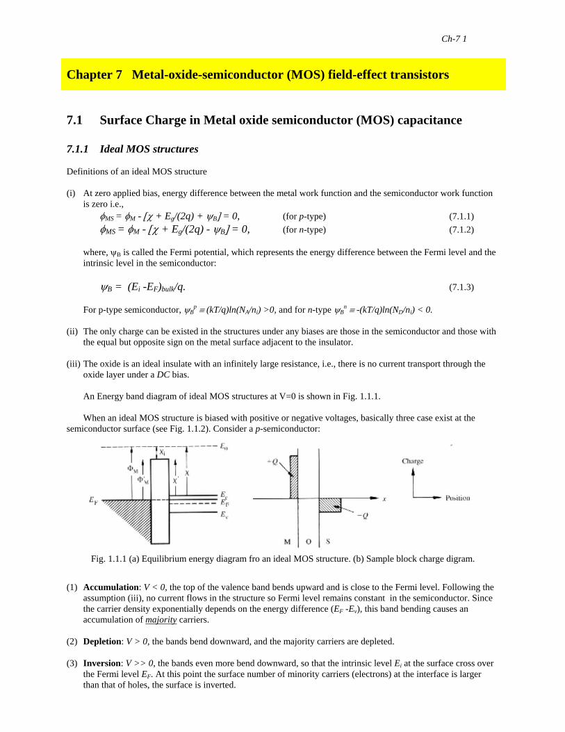
Ch-7 1 Chapter 7 Metal-oxide-semiconductor (MOS) field-effect transistors 7.1 Surface Charge in Metal oxide semiconductor (MOS) capacitance 7.1.1 Ideal MOS structures Definitions of an ideal MOS structure (i) At zero applied bias, energy difference between the metal work function and the semiconductor work function is zero i.e., φ MS = φ M - [χ + E g /(2q) + ψ B ] = 0, (for p-type) (7.1.1) φ MS = φ M - [χ + E g /(2q) - ψ B ] = 0, (for n-type) (7.1.2) where, ψ B is called the Fermi potential, which represents the energy difference between the Fermi level and the intrinsic level in the semiconductor: ψ B = (E i -E F ) bulk /q. (7.1.3) For p-type semiconductor, ψ B p ≡ (kT/q)ln(N A /n i ) >0, and for n-type ψ B n ≡ -(kT/q)ln(N D /n i ) < 0. (ii) The only charge can be existed in the structures under any biases are those in the semiconductor and those with the equal but opposite sign on the metal surface adjacent to the insulator. (iii) The oxide is an ideal insulate with an infinitely large resistance, i.e., there is no current transport through the oxide layer under a DC bias. An Energy band diagram of ideal MOS structures at V=0 is shown in Fig. 1.1.1. When an ideal MOS structure is biased with positive or negative voltages, basically three case exist at the semiconductor surface (see Fig. 1.1.2). Consider a p-semiconductor: Fig. 1.1.1 (a) Equilibrium energy diagram fro an ideal MOS structure. (b) Sample block charge digram. (1) Accumulation: V < 0, the top of the valence band bends upward and is close to the Fermi level. Following the assumption (iii), no current flows in the structure so Fermi level remains constant in the semiconductor. Since the carrier density exponentially depends on the energy difference (E F -E v ), this band bending causes an accumulation of majority carriers. (2) Depletion: V > 0, the bands bend downward, and the majority carriers are depleted. (3) Inversion: V >> 0, the bands even more bend downward, so that the intrinsic level E i at the surface cross over the Fermi level E F . At this point the surface number of minority carriers (electrons) at the interface is larger than that of holes, the surface is inverted.
Transcript of Chapter 7 Metal-oxide-semiconductor (MOS) field-effect … Note L7_MOS.pdf · 2004-01-18 · Ch-7 1...
Ch-7 1
Chapter 7 Metal-oxide-semiconductor (MOS) field-effect transistors 7.1 Surface Charge in Metal oxide semiconductor (MOS) capacitance 7.1.1 Ideal MOS structures Definitions of an ideal MOS structure (i) At zero applied bias, energy difference between the metal work function and the semiconductor work function
is zero i.e., φMS = φM - [χ + Eg/(2q) + ψB] = 0, (for p-type) (7.1.1) φMS = φM - [χ + Eg/(2q) - ψB] = 0, (for n-type) (7.1.2) where, ψB is called the Fermi potential, which represents the energy difference between the Fermi level and the intrinsic level in the semiconductor: ψB = (Ei -EF)bulk/q. (7.1.3) For p-type semiconductor, ψB
p ≡ (kT/q)ln(NA/ni) >0, and for n-type ψBn ≡ -(kT/q)ln(ND/ni) < 0.
(ii) The only charge can be existed in the structures under any biases are those in the semiconductor and those with
the equal but opposite sign on the metal surface adjacent to the insulator. (iii) The oxide is an ideal insulate with an infinitely large resistance, i.e., there is no current transport through the
oxide layer under a DC bias. An Energy band diagram of ideal MOS structures at V=0 is shown in Fig. 1.1.1. When an ideal MOS structure is biased with positive or negative voltages, basically three case exist at the semiconductor surface (see Fig. 1.1.2). Consider a p-semiconductor:
Fig. 1.1.1 (a) Equilibrium energy diagram fro an ideal MOS structure. (b) Sample block charge digram.
(1) Accumulation: V < 0, the top of the valence band bends upward and is close to the Fermi level. Following the assumption (iii), no current flows in the structure so Fermi level remains constant in the semiconductor. Since the carrier density exponentially depends on the energy difference (EF -Ev), this band bending causes an accumulation of majority carriers.
(2) Depletion: V > 0, the bands bend downward, and the majority carriers are depleted. (3) Inversion: V >> 0, the bands even more bend downward, so that the intrinsic level Ei at the surface cross over
the Fermi level EF. At this point the surface number of minority carriers (electrons) at the interface is larger than that of holes, the surface is inverted.
Ch-7 2
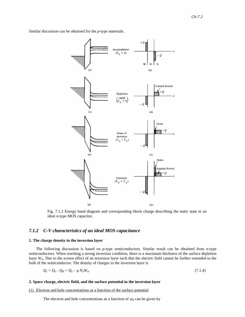
Similar discussion can be obtained for the p-type materials.
Fig. 7.1.2 Energy band diagram and corresponding block charge describing the static state in an ideal n-type MOS capacitor.
7.1.2 C-V characteristics of an ideal MOS capacitance 1. The charge density in the inversion layer
The following discussion is based on p-type semiconductors. Similar result can be obtained from n-type semiconductors. When reaching a strong inversion condition, there is a maximum thickness of the surface depletion layer Wm. Due to the screen effect of an inversion layer such that the electric field cannot be further extended to the bulk of the semiconductor. The density of charges in the inversion layer is
Qs = Qn - QB = Qn - q NAWm (7.1.4) 2. Space charge, electric field, and the surface potential in the inversion layer
(1) Electron and hole concentrations as a function of the surface potential The electron and hole concentrations as a function of ψB can be given by
Ch-7 3
pp = niexp[(Ei(x) - EF)/(kT)] = niexp[q(ψB - ψ(x))/(kT)] = pp0exp[-qψ(x)/(kT)], (7.1.5) np = niexp[( EF - Ei(x))/(kT)] = niexp[q(ψ(x)- ψB)/(kT)] = np0exp[qψ(x)/(kT)], (7.1.6) At the surface: ps = pp0exp[-qψs/(kT)], (7.1.7) np= np0exp exp[qψs/(kT)], (7.1.8) Discussion: Following Eqs. 7.1.7 and 7.1.8, the following regions of surface potential can be distinguished:
ψs < 0 Accumulation of holes (bands bend upward) ψs = 0 Flat band condition ψB > ψs > 0 Depletion of holes (bands bend downward) ψs = ψB Midgap with ns = ps = ni (intrinsic concentration) ψs > ψB Inversion (electron enhancement, bands bend downward) (2) Electric field and electrostatic potential at the surface The electric field and electrostatic potential as a function of distance can be obtained by using 1-D Poisson equation
ddx
x
s
2
2
ψ ρε
= −( )
, (7.1.9)
where, the total space charge density is given by ρ(x) = q(ND
+ - NA- + pp0 - np0). (7.1.10)
In the bulk of the semiconductor, far from the surface, charge neutrality must exist. Therefore, ρbulk = 0, (7.1.11) ND
+ - NA- = pp0 - np0, (7.1.12)
which yields the boundary conditions,
ψbulk = 0 (7.1.13) dψ/dx|bulk = 0 (7.1.14) In general, from Eqs. 7.1.7 and 7.1.8, for any value of ψ(x)we have
p n pqkT
nqkTp p p p− = − −0 0exp( ) exp( )
ψ ψ (7.1.15)
Eq. 7.1.9 can be rewritten as
ddx
qp
qkT
nqkTs
p p
2
2 0 0
ψε
ψ ψ= − − −
⎡⎣⎢
⎤⎦⎥
exp( ) exp( ) . (7.1.16)
Integrating Eq. 7.1.16 from the bulk toward the surface
∂ ψ∂
∂ ψ∂ ε
ψ ψψ
∂ ψ ∂ ψ
xd
xq
pqkT
nqkT
dx
sp p( ) exp( ) exp( )
/
0 0 00∫ ∫= − − −⎡⎣⎢
⎤⎦⎥
. (7.1.17)
Hence, the electric field
Ch-7 4
rE
xkT
qLF
qkT
npD
p
p
2 2 0
0
22
= − =⎡
⎣⎢⎢
⎤
⎦⎥⎥
( ) ( ) ( , )∂ ψ∂
ψ, (7.1.18)
where,
LkT
q pDs
p=
22
0
ε, (7.1.19)
is called the extrinsic Debye length of holes, and
FqkT
np
p
p( , )ψ 0
0= exp( ) (exp( )
/
− + −⎡⎣⎢
⎤⎦⎥+ − −
⎡⎣⎢
⎤⎦⎥
⎧⎨⎪
⎩⎪
⎫⎬⎪
⎭⎪qkT
qkT
np
qkT
qkT
p
p
ψ ψ ψ ψ1 10
0
1 2
≥ 0 (7.1.20)
Therefore,
Ex
kTqL
FqkT
npx
D
p
p= − = ±
∂ ψ∂
ψ2 0
0( , ) . (7.1.21)
Discussion: (i) Ex with positive sign means positive voltage is applied on the metal gate, the direction of
electric field is from the metal gate to the semiconductor. The surface potential bends downward.
(ii) Ex with negative sign means negative voltage is applied on the metal gate, the direction of electric field is from the semiconductor to the metal gate to. The surface potential bends upward.
(3) Space charge density at the surface region By Gauss’s law, the space charge per unit area required to produce the electric field at the surface is
Q E xkT
qLF
qkT
nps s s s
D
s p
p= − = = =ε ψ ψ
ψ( , ) ( ,0
2 0
0m ) . (7.1.22)
Discussion: (i) ψs < 0 and Qs < 0 correspond to the hole accumulation region, Qs ∝ exp[q|ψs |/(kT)] (ii) ψs = 0 and Qs = 0 correspond to the flat band; (iii) ψF > ψs > 0 and Qs < 0 correspond to the hole depletion, Qs ∝ (ψs )1/2
(iv) ψs >> ψF, i.e., the surface inversion, Qs ∝ exp[qψs /(2kT)]. Note that the strong surface inversion begins at the surface potential
ψs(inv) = 2ψB = (2kT/q)ln(NA/ni) (7.1.23) (4) Surface depletion layer width When ψs = 2ψB, the width of the surface depletion region reaches a maximum value. That is because when the bands are bent down far enough that ψs = 2ψB, the semiconductor is shielded from further penetration of the electric field by the inversion layer and even a small increase in band bending results in a very large increase in the charge density within the inversion layer. This situation can be approached to a one-side abrupt p-n junction, where, the charge density in the depletion region is given by ρ(x) = -qNA/W. The solution of Poisson’s equation is
ψ(x) = ψs(1 - x/W)2, (7.1.24)
where, ψs = qNAW2/(2εs). (7.1.25)
Ch-7 5
The maximum width of the surface depletion region under surface steady-state can be obtained from Eq. 7.1.23 and 7.1.24
Winv
qNkT N n
qNms s
A
s A
A= =
2 4ε ψ ε( ) ln( / )i . (7.1.26)
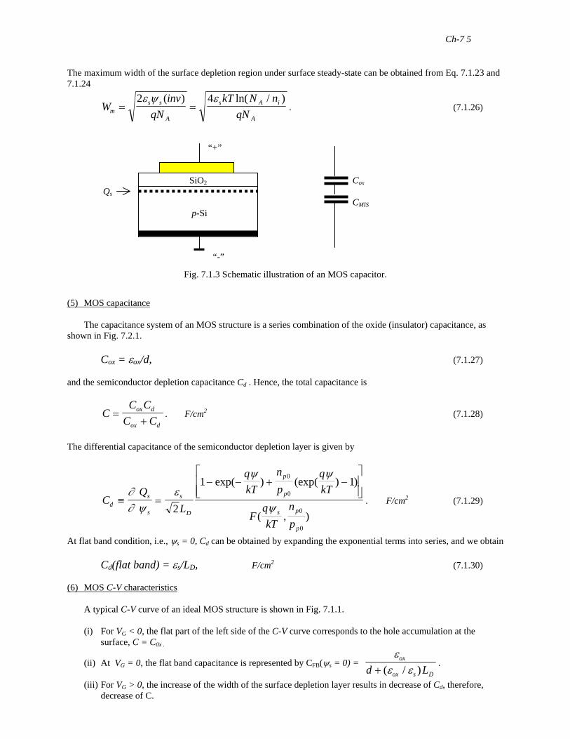
“+” SiO2 Cox Qs CMIS p-Si “-”
Fig. 7.1.3 Schematic illustration of an MOS capacitor. (5) MOS capacitance The capacitance system of an MOS structure is a series combination of the oxide (insulator) capacitance, as shown in Fig. 7.2.1. Cox = εox/d, (7.1.27) and the semiconductor depletion capacitance Cd . Hence, the total capacitance is
C . F/cmC C
C Cox d
ox d=
+2 (7.1.28)
The differential capacitance of the semiconductor depletion layer is given by
CQ
L
qkT
np
qkT
FqkT
np
ds
s
s
D
p
p
s p
p
≡ =
− − + −⎡
⎣⎢⎢
⎤
⎦⎥⎥∂
∂ ψε
ψ ψ
ψ2
1 10
0
0
0
exp( ) (exp( ) )
( , ). F/cm2 (7.1.29)
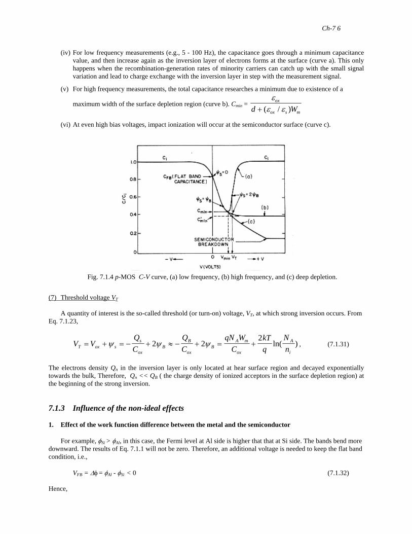
At flat band condition, i.e., ψs = 0, Cd can be obtained by expanding the exponential terms into series, and we obtain Cd(flat band) = εs/LD, F/cm2 (7.1.30) (6) MOS C-V characteristics A typical C-V curve of an ideal MOS structure is shown in Fig. 7.1.1. (i) For VG < 0, the flat part of the left side of the C-V curve corresponds to the hole accumulation at the surface, C = C0x .
(ii) At VG = 0, the flat band capacitance is represented by CFB(ψs = 0) = ε
ε εox
ox s Dd L+ ( / ).
(iii) For VG > 0, the increase of the width of the surface depletion layer results in decrease of Cd, therefore, decrease of C.
Ch-7 6
(iv) For low frequency measurements (e.g., 5 - 100 Hz), the capacitance goes through a minimum capacitance value, and then increase again as the inversion layer of electrons forms at the surface (curve a). This only happens when the recombination-generation rates of minority carriers can catch up with the small signal variation and lead to charge exchange with the inversion layer in step with the measurement signal.
(v) For high frequency measurements, the total capacitance researches a minimum due to existence of a
maximum width of the surface depletion region (curve b). Cmin = ε
ε εox
ox s md W+ ( / )
(vi) At even high bias voltages, impact ionization will occur at the semiconductor surface (curve c).
Fig. 7.1.4 p-MOS C-V curve, (a) low frequency, (b) high frequency, and (c) deep depletion.
(7) Threshold voltage VT A quantity of interest is the so-called threshold (or turn-on) voltage, VT, at which strong inversion occurs. From Eq. 7.1.23,
V VQC
QC
qN WC
kTq
NnT ox s
s
oxB
B
oxB
A m
ox
A
i= + = − + ≈ − + = +ψ ψ ψ2 2
2ln( ) , (7.1.31)
The electrons density Qn in the inversion layer is only located at hear surface region and decayed exponentially towards the bulk, Therefore, Qn << QB ( the charge density of ionized acceptors in the surface depletion region) at the beginning of the strong inversion. 7.1.3 Influence of the non-ideal effects 1. Effect of the work function difference between the metal and the semiconductor For example, φSi > φAl, in this case, the Fermi level at Al side is higher that that at Si side. The bands bend more downward. The results of Eq. 7.1.1 will not be zero. Therefore, an additional voltage is needed to keep the flat band condition, i.e., VFB = ∆φ = φAl - φSi < 0 (7.1.32) Hence,
Ch-7 7
VqN W
CkTq
Nn
VTA m
ox
A
iFB= + +
2ln( ) . (7.1.33)
2. Effects of the oxide charges and interface trapped charges Oxide charges include:
(i) The oxide fixed charge Qf, caused by excess Si (trivalent Si) or loss of an electron from excess oxygen centers (non-bridging oxygen) near the Si/SiO2 interface. It is 2-D in character.
(ii) The oxide trapped charge Qot, associate with defects in SiO2. The oxide traps are usually electrically neutral. But under an electric field, electrons can be drifted towards the metal side, and remain inmobile positively charge center in the oxide layer.
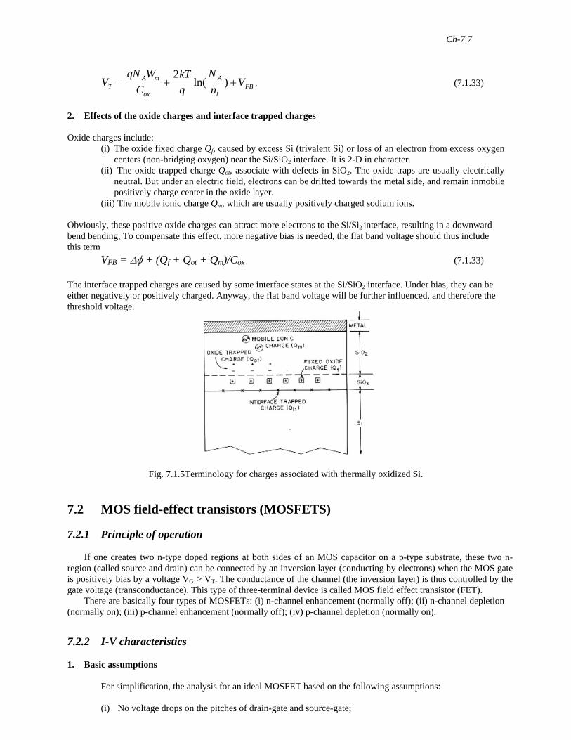
(iii) The mobile ionic charge Qm, which are usually positively charged sodium ions. Obviously, these positive oxide charges can attract more electrons to the Si/Si2 interface, resulting in a downward bend bending, To compensate this effect, more negative bias is needed, the flat band voltage should thus include this term VFB = ∆φ + (Qf + Qot + Qm)/Cox (7.1.33) The interface trapped charges are caused by some interface states at the Si/SiO2 interface. Under bias, they can be either negatively or positively charged. Anyway, the flat band voltage will be further influenced, and therefore the threshold voltage.
Fig. 7.1.5Terminology for charges associated with thermally oxidized Si. 7.2 MOS field-effect transistors (MOSFETS) 7.2.1 Principle of operation If one creates two n-type doped regions at both sides of an MOS capacitor on a p-type substrate, these two n-region (called source and drain) can be connected by an inversion layer (conducting by electrons) when the MOS gate is positively bias by a voltage VG > VT. The conductance of the channel (the inversion layer) is thus controlled by the gate voltage (transconductance). This type of three-terminal device is called MOS field effect transistor (FET). There are basically four types of MOSFETs: (i) n-channel enhancement (normally off); (ii) n-channel depletion (normally on); (iii) p-channel enhancement (normally off); (iv) p-channel depletion (normally on). 7.2.2 I-V characteristics 1. Basic assumptions For simplification, the analysis for an ideal MOSFET based on the following assumptions: (i) No voltage drops on the pitches of drain-gate and source-gate;
Ch-7 8
(ii) The carrier mobility in the inversion layer in constant (constant mobility mold); (iii) The current component in the channel in a drift current;
(iv) The reverse saturation current between the channel and the substrate is zero ; (v) The perpendicular component of the electric field (Ey) to keep the electric charge density in the
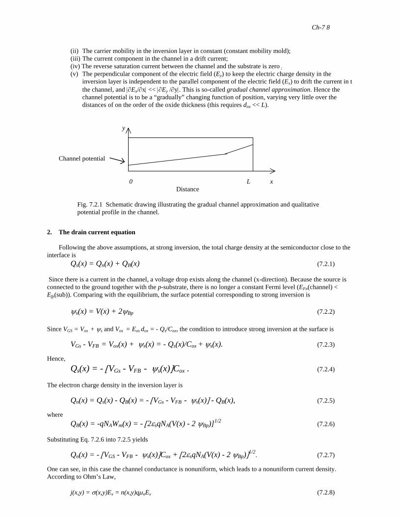
inversion layer is independent to the parallel component of the electric field (Ex) to drift the current in t the channel, and |∂Ex/∂x| << |∂Ey /∂y|. This is so-called gradual channel approximation. Hence the channel potential is to be a “gradually” changing function of position, varying very little over the distances of on the order of the oxide thickness (this requires dox << L).
y Channel potential
0 L x Distance
Fig. 7.2.1 Schematic drawing illustrating the gradual channel approximation and qualitative potential profile in the channel.
2. The drain current equation Following the above assumptions, at strong inversion, the total charge density at the semiconductor close to the interface is Qs(x) = Qn(x) + QB(x) (7.2.1) Since there is a current in the channel, a voltage drop exists along the channel (x-direction). Because the source is connected to the ground together with the p-substrate, there is no longer a constant Fermi level (EFn(channel) < Efp(sub)). Comparing with the equilibrium, the surface potential corresponding to strong inversion is ψs(x) = V(x) + 2ψBp (7.2.2) Since VGS = Vox + ψs and Vox = Eox dox = - Qs/Cox, the condition to introduce strong inversion at the surface is
VGs - VFB = Vox(x) + ψs(x) = - Qs(x)/Cox + ψs(x). (7.2.3) Hence, Qs(x) = - [VGs - VFB - ψs(x)]Cox . (7.2.4) The electron charge density in the inversion layer is
Qn(x) = Qs(x) - QB(x) = - [VGs - VFB - ψs(x)] - QB(x), (7.2.5) where QB(x) = -qNAWm(x) = - [2εsqNA(V(x) - 2 ψBp)]1/2 (7.2.6) Substituting Eq. 7.2.6 into 7.2.5 yields
Qn(x) = - [VGS - VFB - ψs(x)]Cox + [2εsqNA(V(x) - 2 ψBp)]1/2. (7.2.7) One can see, in this case the channel conductance is nonuniform, which leads to a nonuniform current density. According to Ohm’s Law, j(x,y) = σ(x,y)Ex = n(x,y)qµnEx (7.2.8)
Ch-7 9
Following the gradual channel approximation, Ex is only a function of position x, Ex = -dV/dx , and also the constant mobility model, one can integrate the Eq 7.2.8 over the cross section area of the channel, which yields the total channel current
ID(x) = ZµnQn(dV/dx) (7.2.9) Integrating the above equation from drain to source
[ ] [ ]{ }I dx Z V V V x C qN V x dVD n GS FB Bp ox s A Bp
VL DS= − − − − −∫∫ µ ψ ε( ) ( )2 2 2
00ψ ,
(7.2.10) we obtain
[ ]IZ C
LV V
VV
qNC
VDn ox
GS FBDS
Bp DSs A
oxDS Bp Bp= − − −
⎡⎣⎢
⎤⎦⎥
− + −⎧⎨⎪
⎩⎪
⎫⎬⎪
⎭⎪
µψ
εψ ψ
22
23
22 23 2 2 3( ) ( )/ /
(7.2.11) The above derivation is based on a uniform channel with good conductance between drain and source, therefore, it describes the non-saturated I-V of the output characteristics.
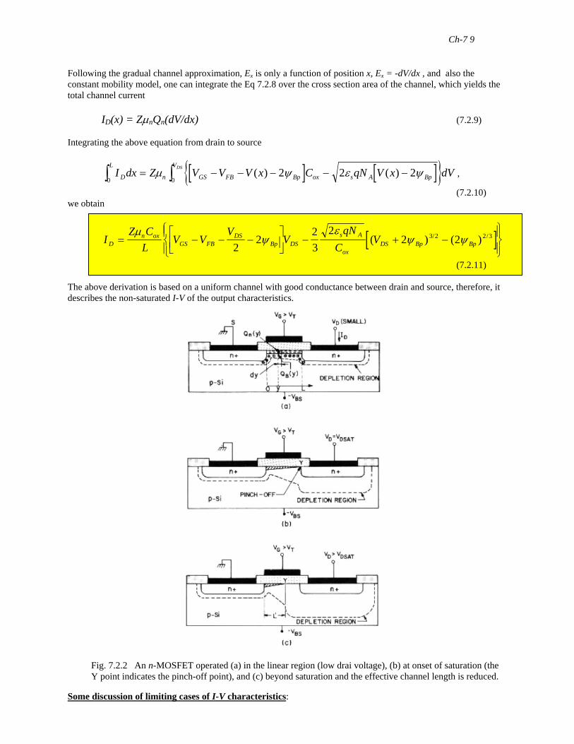
Fig. 7.2.2 An n-MOSFET operated (a) in the linear region (low drai voltage), (b) at onset of saturation (the Y point indicates the pinch-off point), and (c) beyond saturation and the effective channel length is reduced.
Some discussion of limiting cases of I-V characteristics:
Ch-7 10
(1) Linear region: If VDS < ψBp, we can use the following approximation, (VDS + 2 ψBp)3/2 ≈ ( 2 ψBp)3/2 [1 + 3/2 + VDS/(2 ψBp)], (7.2.12) and substitute it into Eq. 7.2.11. We find
IZ C
LV V
qN
CV
VD
n oxGS FB Bp
s A Bp
oxDS
DS≈ − − −⎡
⎣⎢⎢
⎤
⎦⎥⎥
−⎧⎨⎪
⎩⎪
⎫⎬⎪
⎭⎪
µψ
ε ψ2
2 2
2
2( ). (7.2.13)
As we have known, the threshold voltage for an n-MOS is
VqN
CVT
s A Bp
oxBp FB= +
2 22
ε ψψ
( )+ . (7.2.14)
Substituting Eq. 7.14 into 7.1.3, we obtain an express for ID under a very small VDS.
[ ]IZ C
LV V V
VD
n oxGS T DS
DS≈ − −⎧⎨⎩
⎫⎬⎭
µ 2
2. (7.2.15)
If VDS << (VGS - VT), we find
[ ]IZ C
LV V VD
n oxGS T DS≈ −
µ. (7.2.16)
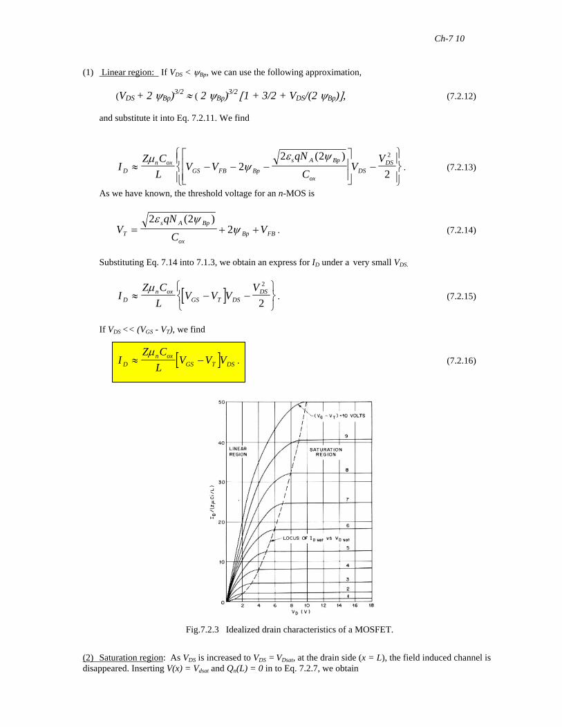
Fig.7.2.3 Idealized drain characteristics of a MOSFET.
(2) Saturation region: As VDS is increased to VDS = VDsat, at the drain side (x = L), the field induced channel is disappeared. Inserting V(x) = Vdsat and Qn(L) = 0 in to Eq. 7.2.7, we obtain
Ch-7 11
V V V KV V
KDsat GS FB BpGS FB= − − + − +−⎡
⎣⎢
⎤
⎦⎥2 1 1
222ψ
( ), (7.2.17)
where, K = (εsqNA)1/2/Cox. Substituting Eq. 7.1.7 into 7.2.11, we find an expression for the drain saturation current
[ ]IZ C
LV V
VV K VDsat
n oxGS FB
DsatBp Dsat Dsat Bp Bp= − − −
⎡⎣⎢
⎤⎦⎥
− + −⎧⎨⎩
⎫⎬⎭
µψ ψ
22
23
2 2 23 2 2 3( ) (/ /ψ ) .
(7.2.18) If the substrate doping is low, and the oxide layer is thin, K2 << 1, we have the following approximation
1 12
22− +−⎡
⎣⎢ . (7.2.19)
⎤
⎦⎥ ≈ − −
( )( )
V VK
K V VGS FBGS FB
Eq. 7.2.17 can be re-written as
Vdsat = VGS - VT’ (7.2.20) where,
VT’ = VFB + 2ψBp + K [2(VGS - VFB)]1/2, (7.2.21) And under such a condition, the drain saturation current can be presented by
IZ C
LV V
Z CL
VDsatn ox
GS Tn ox
Dsat≈ − =µ µ
( )' 2 2 . (7.2.22)
3. Channel conductance The most important small signal parameter of MOSFETs is transconductance, gm. (1) In the linear saturation regime, gm can be obtained by differentiating E. 7.2.16, with respect to the gate voltage.
gI
VZL
C VmD
GSV const n ox DSDS
≡ ==
∂∂
µ . (VDS < VGS - VT) (7.2.23)
(2) In the saturation regime, gm can be obtained by differentiating Eq. 7.2.22,
∂∂
µIV
ZL
C V VDsat
GSV const n ox GS TDS =
= −( ) . (VDS > VGS - VT) (7.2.24)
4. Operation frequency limits For MOSFETs, the cut-off frequency, fT is limited by carrier transit time, τtr, in the channel.
τυ µ µtr
eff n x n DS
L LE
LV
= = =2
. (7.2.25)
Hence,
Ch-7 12
f Ttr
=1
2π τ. (7.2.26)
Since gm ∼ Coxυeff/L, τtr = Ctotal/gm. Hence, we find
fg
C C CTm
GS M p=
+ +2π ( ), (7.2.27)
where, CGS = CoxZ(L + ∆LDS) (∆LDS: overlap between the gate and the source) CM = CGD(1 + gmRL) is called the miller capacitance. CM is any parasitic capacitance. Eq. 7.2.27 presents the importance of the device dimension to the device speed scale. If the channel length is very short, the carrier transport in the channel will be limited by the carrier velocity saturation, fT should thus be expressed as
fLT
sat=υπ2
. (7.2.28)
As has been discussed in the chapter 5, the unilateral power gain (U), which exists when the output-input feedback in the transistor is canceled by another feedback network with both the input and output pots conjugately matched, is regardless of the stability of the amplifier, and variant under lossless reciprocal embedding. It is thus a better figure to describe how transistor can be used for microwave and millimeter-wave applications,
Uff
≈⎛⎝⎜
⎞⎠⎟max
2
. (7.2.29)
Hence,
ff
R R R r f R C
T
G i S ds T G GD
max
( ) /=
+ + +⎡
⎣⎢
⎤
⎦⎥2 2π
. (7.2.30)
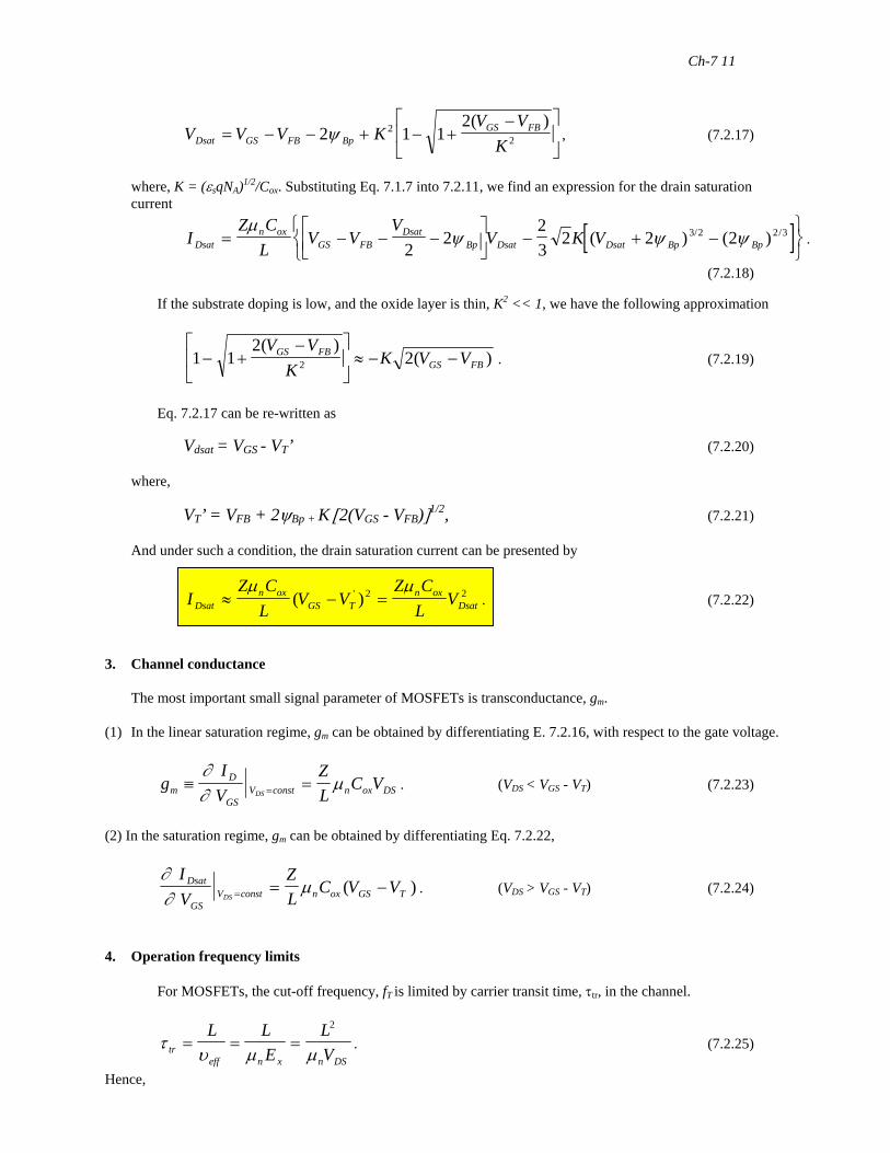
The value of fmax of a FET may be higher or lower than its fT, upon the various series resistances and CGD. The small signal equivalent circuit of a MOSFET is given in Fig. 7.2.4
Fig. 7.2.4 Equivalent circuit of a MOSFET
Ch-7 13
7.2.3 Limitations and perspectives of MOSFETS The above section, the basic theory of MOSFET operation was described and equations that frequently used in the circuit design were derived. This theory contains a number of approximations that limits its accuracy. It also failed to account for several important physical effects occurring in MOSFETs. In this section, we will discuss these important limitations of MOSFETs, in particular, of short channel MOSFETs. 1. Subthreshold current The theory for the drain current that we have discussed approximates the channel conductance by assuming that the channel does not conductive unless the gate voltage exceeds the threshold voltage. Therefore, it fails to predict the subthreshold current arising from the (weak) inversion charge that exists at gate voltage below the conventional threshold voltage. The subthreshold region is particularly important for low-voltage, low power applications. In weak inversion, the drain current is dominated by diffusion and is derived in the same way as the collector current in a BJT with homogeneous base doping. Considering the n-MOSFET as an n-p-n BJT
I qA Ddndx
qA Dn n L
LD eff n eff n= − =−( ) ( )0
, (7.2.31)
where, Aeff ≈ Zdc is the effective cross section of current flow, dc ≈ kT/[qEy(0)], and n(0) = np0 exp[qV(y)/(kT)], (7.2.32)
n(L) = np0 exp[q(V(y)-VDS)/(kT)]. (7.2.33) Here, V(y) is the electric potential that is given by
V(y) ≈ ψs - Eyy, (7.2.34) and Ey = |QB|/εs = (2qψsNA/εs)1/2 (7.2.35) Substituting Eqs. 7.2.32 and 7.2.33 into 7.2.31 gives
I
ZL
KTq
nN
kTq
qkT
qVkT
LDsat
s ni
A s
s D
Dp
=−
⎡⎣⎢
⎤⎦⎥
ε µψ
ψ( )( ) ( ) exp( ) exp( )/2 1 2 1
2
S
. (7.2.36)
The surface potential can be expressed as a function of the gate voltage,
VGS = Vox + ψs + VFB . (7.2.37) where,
Vox = Ey(0)doxεs/εox. (7.2.38)
Using Eq. 7.2.33, 7.35, and 7.3.36, we find ψs = VGS - VFB + as
2 - as[ as2 + 2(VGS -VFB)]1/2 (7.2.39)
where as = (qNAεs)1/2dox/εox. (7.2.40)
Ch-7 14
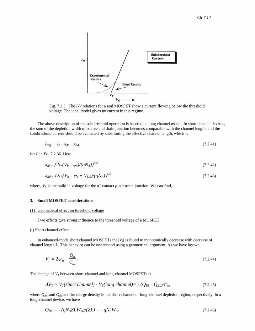
Fig. 7.2.5 The I-V relations for a real MOSFET show a current flowing below the threshold voltage. The ideal model gives no current in this regime.
The above description of the subthreshold operation is based on a long channel model. In short channel devices, the sum of the depletion width of source and drain junction becomes comparable with the channel length, and the subthreshold current should be evaluated by substituting the effective channel length, which is Leff = L - xds - xdd, (7.2.41) for L in Eq. 7.2.36. Here xds = [2εs(Vb - ψs)/(qNA)]1/2 (7.2.42) xdd = [2εs(Vb - ψs + VDS)/(qNA)]1/2 (7.2.43) where, Vb is the build in voltage for the n+ contact p-substrate junction. We can find, 3. Small MOSFET considerations (1) Geometrical effect on threshold voltage Two effects give strong influence to the threshold voltage of a MOSFET. (i) Short channel effect In enhanced-mode short channel MOSFETs the |VT| is found to monotonically decrease with decrease of channel length L. This behavior can be understood using a geometrical argument. As we have known,
VQCT B
B
ox= −2ψ . (7.2.44)
The change of VT between short-channel and long-channel MOSFETs is ∆VT = VT(short channel) - VT(long channel)= - (QBS - QBL)/Cox, (7.2.45) where QBS and QBL are the charge density in the short-channel or long-channel depletion region, respectively. In a long-channel device, we have QBL = - (qNAZLWm)/(ZL) = - qNAWm. (7.2.46)
Ch-7 15
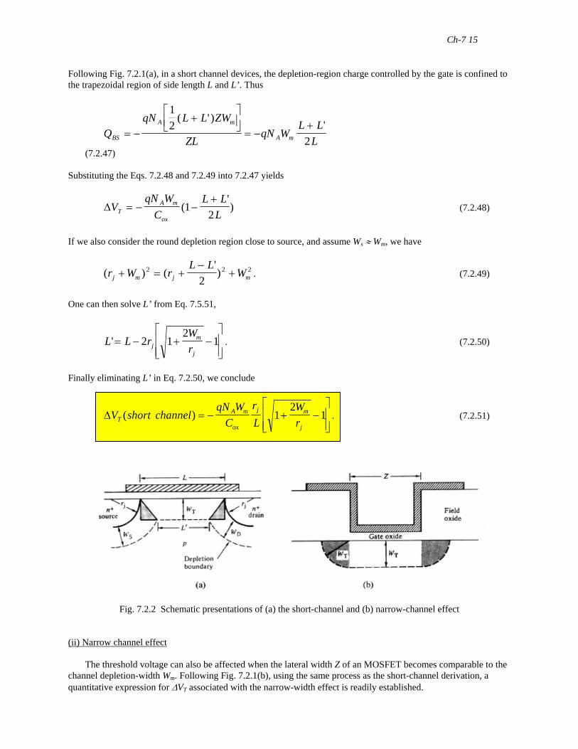
Following Fig. 7.2.1(a), in a short channel devices, the depletion-region charge controlled by the gate is confined to the trapezoidal region of side length L and L’. Thus
QqN L L ZW
ZLqN W
L LLBS
A m
A m= −+
⎡⎣⎢
⎤⎦⎥ = −
+12
2
( ' ) '
(7.2.47) Substituting the Eqs. 7.2.48 and 7.2.49 into 7.2.47 yields
∆VqN W
CL L
LTA m
ox= − −
+(
')1
2 (7.2.48)
If we also consider the round depletion region close to source, and assume Ws ≈ Wm, we have
( ) (')r W r
L LWj m j+ = +
−+2
2 m2 2 . (7.2.49)
One can then solve L’ from Eq. 7.5.51,
L L rWrj
m
j'= − + −
⎡
⎣⎢⎢
⎤
⎦⎥⎥
2 12
1 . (7.2.50)
Finally eliminating L’ in Eq. 7.2.50, we conclude
∆V short channelqN W
CrL
WrT
A m
ox
j m
j( ) = − + −
⎡
⎣⎢⎢
⎤
⎦⎥⎥
12
1 . (7.2.51)
Fig. 7.2.2 Schematic presentations of (a) the short-channel and (b) narrow-channel effect (ii) Narrow channel effect The threshold voltage can also be affected when the lateral width Z of an MOSFET becomes comparable to the channel depletion-width Wm. Following Fig. 7.2.1(b), using the same process as the short-channel derivation, a quantitative expression for ∆VT associated with the narrow-width effect is readily established.
Ch-7 16
Q narrow widthqN ZLW W L
ZLqN W
WZBS
A m m
A mm( ) (= −
+⎡⎣⎢
⎤⎦⎥ = − +
ππ2
12
2
) . (7.2.52)
Replacing QBS in Eq. 7.2.52 with Eq. 7.2.59, one concludes,
∆V narrow channelqN W
CWZT
A m
ox
m( ) =π2
(7.2.53)
The above discussion showed that parameters such as the threshold voltage, etc., for short-channel MOSFETs depend not only on the device length but also (for narrow devices) on the device width because of the fringing fields that increase the threshold voltage. (2) Hot carriers As has been discussed before, electrons can gain energy from the electric field. At a very high field, which is a case for short-channel MOSFETs, electrons can be very hot. Several effects can be introduced by hot electrons.
(i) Oxide charging: Oxide charging, or charge injection and trapping in the oxide is a phenomenon that occurs in all MOSFETs, which in turn results in significant changes in VT and gm. Since the electric field in a short channel MOSFET is high, free carrier passing through the high-field region near the drain can easily gain sufficient energy, this effect is thus stronger. (ii) Channel velocity saturation At high electric fields, the increase of the carrier mobility as a function of the field is getting slow and is no longer linearly proportional to the strength of the field. At very high electric fields, the carrier transport velocity becomes independent of the field, which is called the velocity saturation. In case of a short channel MOSFET, the VDS across the gate length gives rise to a very high electric field. If we ground the source, the electric field at the drain side is
E(L) = Vs-d/L (7.2.54) The expressions of the drain saturation voltage and drain saturation current should be modified by
Vdsat = VGT + Vs-d - (VGT2
+ Vs-d 2)1/2 (7.2.55)
where, VGT = VGS -VT, and
IDsat = β Vs-d 2 [1 + (VGT/Vs-d)2]1/2 - β Vs-d
2, (7.2.56) where, β = µn(Z/L)Cox. Discussion: Two extreme cases:
(i) Vs-d = υsL/µn >> VGT, IDsat = β(VGT)2/2 which is the same expression for long channel devices.
(ii) Vs-d = υsL/µn << VGT, IDsat = βVGT Vs-d and Vdsat → Vs-d << VGT - Vs-d. This means that the drain saturation current is 2Vs-d/VGT times smaller than the value predicted by the constant mobility model.
Ch-7 17
(iii) Velocity overshot/Ballistic transport:
In all discussion, we still assume that the channel length, L, is much greater than the mean scattering distance, λ, of electrons during transport through the channel. When even smaller-dimensional structures could be built with L ≤ λ, however, a large percentage of the electrons would travel from the source to drain without experiencing a single electron scattering event. The envisioned projectile-like motion of the carriers is refereed to as Ballistic transport. It is expected to observed such a phenomenon for the device with the line feature less than 0.1 µm (for Si). Practically speaking, ballistic transport is of interest because it could lead to super-fast devices. With reduced scattering, the average velocity of carriers transversing the channel can exceed υsat. This is referred to as velocity overshot. Average velocities up to 35% larger than the saturation velocity have been observed in an L = 0.12 µm MOSFET (Assaderaghi, 1993).
(3) breakdown When the device dimension becomes very small and the electric field is high, the junction breakdown may play an important role in determining the current-voltage characteristics and carrier distributions in the devices. Basically three breakdowns are discussed
(i) the avalanche breakdown near the drain; (ii) the punchthrough across the channel; (iii) the irreversible breakdown of thin oxide layer when the applied electric field on the gate exceeds the
dielectric strength of the SiO2 ( 7x10⁶ Vcm-1). (4) Injection into oxide For a very short-channel MOSFET, in order to keep charge control mode the gate oxide has to be very thin, e.g., 0.1 µm MOS technology requires the use of ultra thin gate oxide with the thickness lees than 30 Å (the technology has allowed to produce 15 Å thick thermal oxide for the gate purpose.) As the oxide becomes thinner, the gate leakage current, because of increasing direct quantum -mechanic tunneling, becomes significant. For example, for a 25 Å thick film, the current density with a 1 V supply is 0.1 A/cm2. (5) Dopant fluctuation The random fluctuation of number of dopant atoms in the channel of a MOSFET would be a fundamental limitation of MOSFET minimization. As MOSFET scaling approaches the sub-0.1 µm regime, the number of dopants is of the order of hundreds in the depletion region, and less that 100 in the inversion layer, for minimum-geometry devices. As a result, the detailed microscopic dopant distribution in the MOSFET channel will give non-negligible influence on device electric performance.

Ch-7 18
4. Scale MOSs to small size The advantages of building ICs with higher and higher component densities have provided continued impetus for designing MOSFETs with even smaller dimensions. It, however, only surface dimensions are reduced while other circuit and device parameters remain unchanged, many MOSFET properties are degraded. To make a balance, some design parameters need to scaled down by the same factor by which the dimensions are reduced. This is called scaling rules. A commonly accepted rule is Constant field scaling.
Table 7.2.1: Scaling Rules for Constant -Field Scaling
Scaling Factor Surface dimension 1/K Vertical dimension, dox, xj 1/K Impurity concentrations K Current, voltage 1/K Current density K Capacitance (per area) K Transconductance 1 Circuit delay time 1/K Power dissipation 1/K2
Power density 1 Power-delay product 1/K3