channel 600 V, 0.55 Ω typ., 7.5 A MDmesh™ M2 D(2) = 250 µA 2 3 4 V R DS(on) Static drain-source...
12
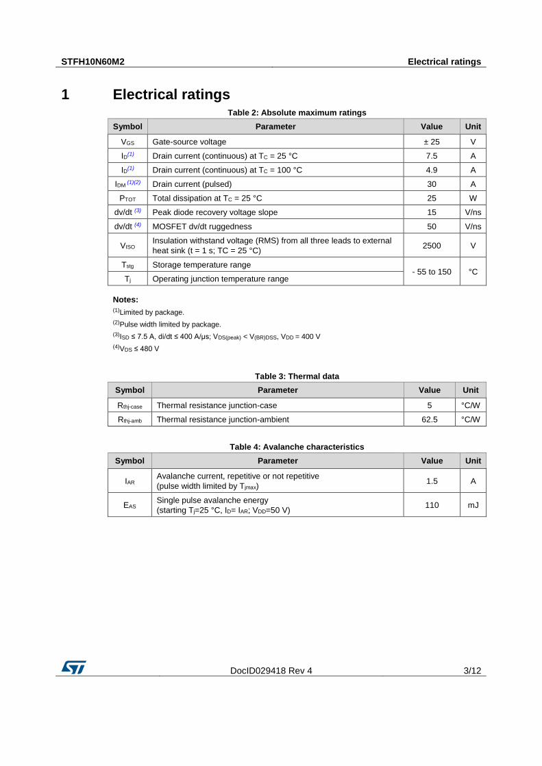
May 2017 DocID029418 Rev 4 1/12 This is information on a product in full production. www.st.com STFH10N60M2 N-channel 600 V, 0.55 Ω typ., 7.5 A MDmesh™ M2 Power MOSFET in a TO-220FP wide creepage package Datasheet - production data Figure 1: Internal schematic diagram Features Order code VDS @ TJmax RDS(on) max ID STFH10N60M2 650 V 0.60 Ω 7.5 A Extremely low gate charge Excellent output capacitance (COSS) profile 100% avalanche tested Zener-protected Wide distance of 4.25 mm between the pins Applications Switching applications LLC converters, resonant converters Description This device is an N-channel Power MOSFET developed using MDmesh™ M2 technology. Thanks to its strip layout and an improved vertical structure, the device exhibits low on-resistance and optimized switching characteristics, rendering it suitable for the most demanding high efficiency converters. The TO-220FP wide creepage package provides increased surface insulation for Power MOSFETs to prevent failure due to arcing, which can occur in polluted environments. Table 1: Device summary Order code Marking Package Packing STFH10N60M2 10N60M2 TO-220FP wide creepage Tube AM15572v1_no_tab D(2) G(1) S(3)
Transcript of channel 600 V, 0.55 Ω typ., 7.5 A MDmesh™ M2 D(2) = 250 µA 2 3 4 V R DS(on) Static drain-source...
May 2017 DocID029418 Rev 4 1/12
This is information on a product in full production. www.st.com
STFH10N60M2
N-channel 600 V, 0.55 Ω typ., 7.5 A MDmesh™ M2 Power MOSFET in a TO-220FP wide creepage package
Datasheet - production data
Figure 1: Internal schematic diagram
Features
Order code VDS @ TJmax RDS(on) max ID
STFH10N60M2 650 V 0.60 Ω 7.5 A
Extremely low gate charge
Excellent output capacitance (COSS) profile
100% avalanche tested
Zener-protected
Wide distance of 4.25 mm between the pins
Applications Switching applications
LLC converters, resonant converters
Description This device is an N-channel Power MOSFET developed using MDmesh™ M2 technology. Thanks to its strip layout and an improved vertical structure, the device exhibits low on-resistance and optimized switching characteristics, rendering it suitable for the most demanding high efficiency converters.
The TO-220FP wide creepage package provides increased surface insulation for Power MOSFETs to prevent failure due to arcing, which can occur in polluted environments.
Table 1: Device summary
Order code Marking Package Packing
STFH10N60M2 10N60M2 TO-220FP wide creepage Tube
AM15572v1_no_tab
D(2)
G(1)
S(3)
Contents STFH10N60M2
2/12 DocID029418 Rev 4
Contents
1 Electrical ratings ............................................................................. 3
2 Electrical characteristics ................................................................ 4
2.1 Electrical characteristics (curves) ...................................................... 6
3 Test circuits ..................................................................................... 8
4 Package information ....................................................................... 9
4.1 TO-220FP wide creepage package information ................................ 9
5 Revision history ............................................................................ 11
STFH10N60M2 Electrical ratings
DocID029418 Rev 4 3/12
1 Electrical ratings Table 2: Absolute maximum ratings
Symbol Parameter Value Unit
VGS Gate-source voltage ± 25 V
ID(1) Drain current (continuous) at TC = 25 °C 7.5 A
ID(1) Drain current (continuous) at TC = 100 °C 4.9 A
IDM (1)(2) Drain current (pulsed) 30 A
PTOT Total dissipation at TC = 25 °C 25 W
dv/dt (3) Peak diode recovery voltage slope 15 V/ns
dv/dt (4) MOSFET dv/dt ruggedness 50 V/ns
VISO Insulation withstand voltage (RMS) from all three leads to external
heat sink (t = 1 s; TC = 25 °C) 2500 V
Tstg Storage temperature range - 55 to 150 °C
Tj Operating junction temperature range
Notes:
(1)Limited by package. (2)Pulse width limited by package. (3)ISD ≤ 7.5 A, di/dt ≤ 400 A/µs; VDS(peak) < V(BR)DSS, VDD = 400 V (4)VDS ≤ 480 V
Table 3: Thermal data
Symbol Parameter Value Unit
Rthj-case Thermal resistance junction-case 5 °C/W
Rthj-amb Thermal resistance junction-ambient 62.5 °C/W
Table 4: Avalanche characteristics
Symbol Parameter Value Unit
IAR Avalanche current, repetitive or not repetitive
(pulse width limited by Tjmax) 1.5 A
EAS Single pulse avalanche energy
(starting Tj=25 °C, ID= IAR; VDD=50 V) 110 mJ
Electrical characteristics STFH10N60M2
4/12 DocID029418 Rev 4
2 Electrical characteristics
(TC = 25 °C unless otherwise specified)
Table 5: On /off states
Symbol Parameter Test conditions Min. Typ. Max. Unit
V(BR)DSS Drain-source breakdown
voltage VGS = 0 V, ID = 1 mA 600
V
IDSS Zero gate voltage drain
current
VGS = 0 V, VDS = 600 V
1 µA
VGS = 0 V, VDS = 600 V,
TC=125 °C (1) 100 µA
IGSS Gate-body leakage current VDS = 0 V, VGS = ±25 V
±10 µA
VGS(th) Gate threshold voltage VDS = VGS, ID = 250 µA 2 3 4 V
RDS(on) Static drain-source on-
resistance VGS = 10 V, ID = 3 A
0.55 0.60 Ω
Notes:
(1)Defined by design, not subject to production test.
Table 6: Dynamic
Symbol Parameter Test conditions Min. Typ. Max. Unit
Ciss Input capacitance
VDS = 100 V, f = 1 MHz,
VGS = 0 V
- 400 - pF
Coss Output capacitance - 22 - pF
Crss Reverse transfer capacitance
- 0.84 - pF
Coss
eq.(1)
Equivalent output
capacitance VDS= 0 to 480 V, VGS= 0 V - 83 - pF
RG Intrinsic gate resistance f = 1 MHz, ID=0 A - 6.4 - Ω
Qg Total gate charge VDD = 480 V, ID = 7.5 A,
VGS = 0 to 10 V
(see Figure 15: "Test circuit for
gate charge behavior")
- 13.5 - nC
Qgs Gate-source charge - 2.1 - nC
Qgd Gate-drain charge - 7.2 - nC
Notes:
(1)Coss eq. is defined as a constant equivalent capacitance giving the same charging time as Coss when VDS
increases from 0 to 80% VDSS
STFH10N60M2 Electrical characteristics
DocID029418 Rev 4 5/12
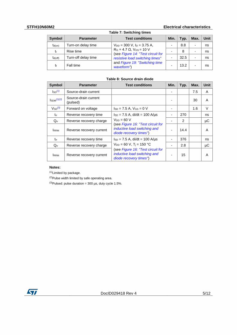
Table 7: Switching times
Symbol Parameter Test conditions Min. Typ. Max. Unit
td(on) Turn-on delay time VDD = 300 V, ID = 3.75 A,
RG = 4.7 Ω, VGS = 10 V
(see Figure 14: "Test circuit for
resistive load switching times"
and Figure 19: "Switching time
waveform")
- 8.8 - ns
tr Rise time - 8 - ns
td(off) Turn-off delay time - 32.5 - ns
tf Fall time - 13.2 - ns
Table 8: Source drain diode
Symbol Parameter Test conditions Min. Typ. Max. Unit
ISD(1) Source-drain current
-
7.5 A
ISDM(1)(2)
Source-drain current
(pulsed) -
30 A
VSD(3) Forward on voltage ISD = 7.5 A, VGS = 0 V -
1.6 V
trr Reverse recovery time ISD = 7.5 A, di/dt = 100 A/µs
VDD = 60 V
(see Figure 16: "Test circuit for
inductive load switching and
diode recovery times")
- 270
ns
Qrr Reverse recovery charge - 2
µC
IRRM Reverse recovery current - 14.4
A
trr Reverse recovery time ISD = 7.5 A, di/dt = 100 A/µs
VDD = 60 V, Tj = 150 °C
(see Figure 16: "Test circuit for
inductive load switching and
diode recovery times")
- 376
ns
Qrr Reverse recovery charge - 2.8
µC
IRRM Reverse recovery current - 15
A
Notes:
(1)Limited by package. (2)Pulse width limited by safe operating area. (3)Pulsed: pulse duration = 300 µs, duty cycle 1.5%.
Electrical characteristics STFH10N60M2
6/12 DocID029418 Rev 4
2.1 Electrical characteristics (curves)
Figure 2: Safe operating area
Figure 3: Thermal impedance
Figure 4: Output characteristics
Figure 5: Transfer characteristics
Figure 6: Gate charge vs gate-source voltage
Figure 7: Static drain-source on-resistance
VGS
6
4
2
00 Qg(nC)
(V)
2
8
10
VDD=480V
300
200
100
0
400
VDS
4
500
VDS
(V)
ID=7.5A
6 8 10 12
12
STFH10N60M2 Electrical characteristics
DocID029418 Rev 4 7/12
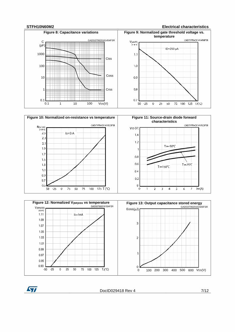
Figure 8: Capacitance variations
Figure 9: Normalized gate threshold voltage vs. temperature
Figure 10: Normalized on-resistance vs temperature
Figure 11: Source-drain diode forward characteristics
Figure 12: Normalized V(BR)DSS vs temperature
Figure 13: Output capacitance stored energy
C
10
1
0.10.1 10 VDS(V)
(pF)
1 100
Ciss
Coss
Crss
100
1000
GADG070620161454FSR
ID=250 µA
ID=3 A
Eoss
0 VDS(V)
(µJ)
200100 5000
1
2
3
300 400 600
GADG070620161505FSR
Test circuits STFH10N60M2
8/12 DocID029418 Rev 4
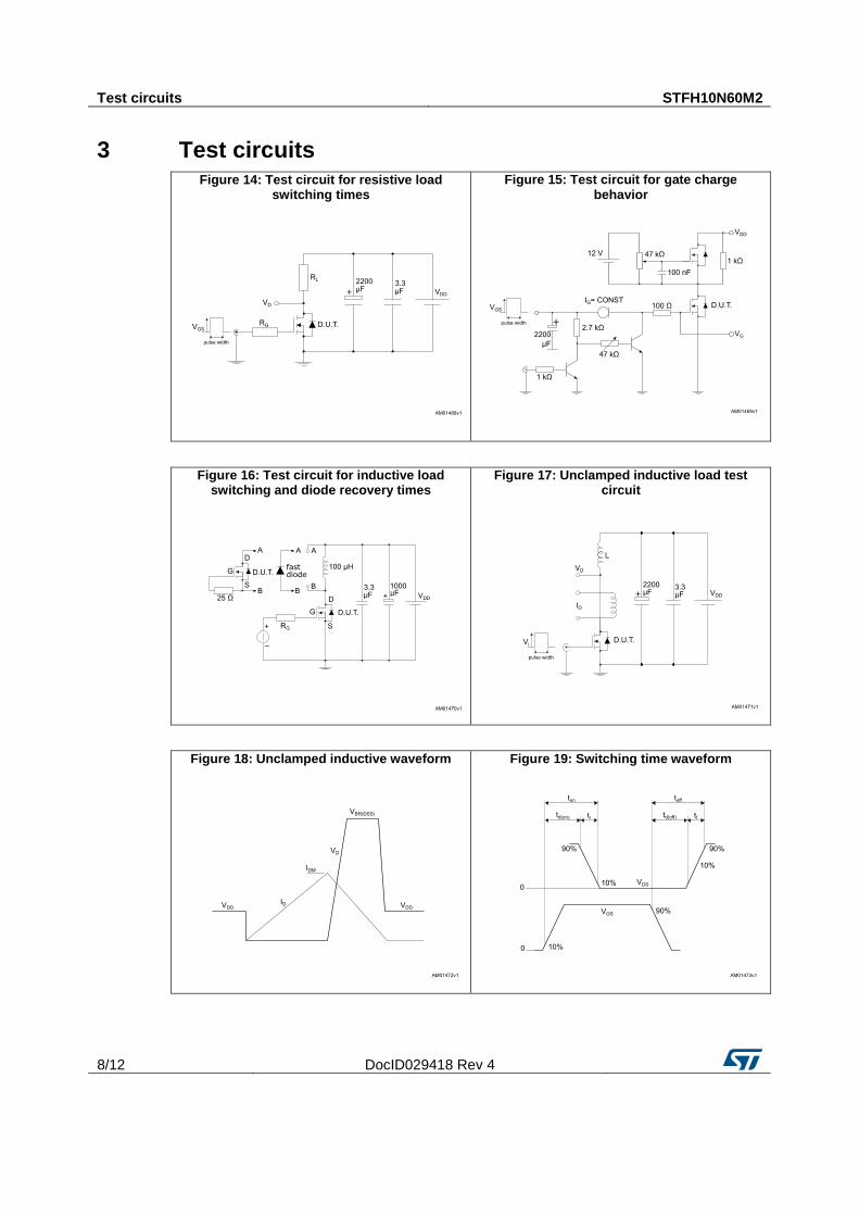
3 Test circuits Figure 14: Test circuit for resistive load
switching times
Figure 15: Test circuit for gate charge behavior
Figure 16: Test circuit for inductive load switching and diode recovery times
Figure 17: Unclamped inductive load test circuit
Figure 18: Unclamped inductive waveform
Figure 19: Switching time waveform
STFH10N60M2 Package information
DocID029418 Rev 4 9/12
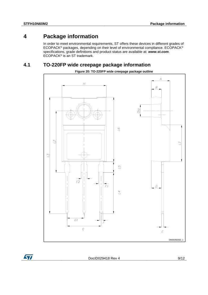
4 Package information
In order to meet environmental requirements, ST offers these devices in different grades of ECOPACK® packages, depending on their level of environmental compliance. ECOPACK® specifications, grade definitions and product status are available at: www.st.com. ECOPACK® is an ST trademark.
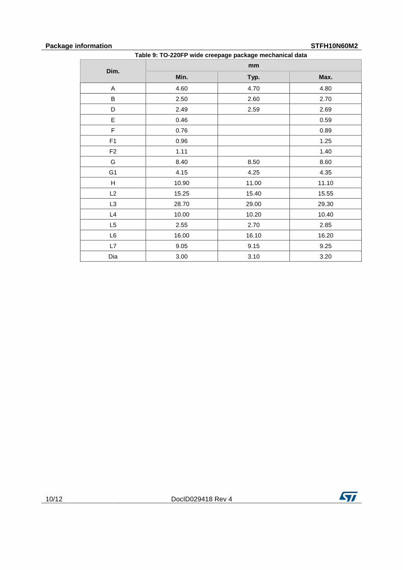
4.1 TO-220FP wide creepage package information
Figure 20: TO-220FP wide creepage package outline
DM00260252_1
Package information STFH10N60M2
10/12 DocID029418 Rev 4
Table 9: TO-220FP wide creepage package mechanical data
Dim. mm
Min. Typ. Max.
A 4.60 4.70 4.80
B 2.50 2.60 2.70
D 2.49 2.59 2.69
E 0.46
0.59
F 0.76
0.89
F1 0.96
1.25
F2 1.11
1.40
G 8.40 8.50 8.60
G1 4.15 4.25 4.35
H 10.90 11.00 11.10
L2 15.25 15.40 15.55
L3 28.70 29.00 29.30
L4 10.00 10.20 10.40
L5 2.55 2.70 2.85
L6 16.00 16.10 16.20
L7 9.05 9.15 9.25
Dia 3.00 3.10 3.20
STFH10N60M2 Revision history
DocID029418 Rev 4 11/12
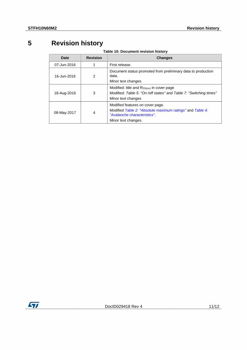
5 Revision history Table 10: Document revision history
Date Revision Changes
07-Jun-2016 1 First release.
16-Jun-2016 2
Document status promoted from preliminary data to production
data.
Minor text changes.
18-Aug-2016 3
Modified: title and RDS(on) in cover page
Modified: Table 5: "On /off states" and Table 7: "Switching times"
Minor text changes
08-May-2017 4
Modified features on cover page.
Modified Table 2: "Absolute maximum ratings" and Table 4:
"Avalanche characteristics".
Minor text changes.
STFH10N60M2
12/12 DocID029418 Rev 4
IMPORTANT NOTICE – PLEASE READ CAREFULLY
STMicroelectronics NV and its subsidiaries (“ST”) reserve the right to make changes, corrections, enhancements, modifications, and improvements to ST products and/or to this document at any time without notice. Purchasers should obtain the latest relevant information on ST products before placing orders. ST products are sold pursuant to ST’s terms and conditions of sale in place at the time of order acknowledgement.
Purchasers are solely responsible for the choice, selection, and use of ST products and ST assumes no liability for application assistance or the design of Purchasers’ products.
No license, express or implied, to any intellectual property right is granted by ST herein.
Resale of ST products with provisions different from the information set forth herein shall void any warranty granted by ST for such product.
ST and the ST logo are trademarks of ST. All other product or service names are the property of their respective owners.
Information in this document supersedes and replaces information previously supplied in any prior versions of this document.
© 2017 STMicroelectronics – All rights reserved


![LABORATÓRIO DE SISTEMAS MECATRÔNICOS E ROBÓTICA ] - LAB.pdf · Resistores - 1,0 Ω - 100k Ω 1,2 Ω - 120k Ω 1,5 Ω - 150k Ω 1,8 Ω- 180k Ω 2,2 Ω– 220k Ω 2,7 Ω– 270k](https://static.fdocument.org/doc/165x107/5c245c1a09d3f224508c4b48/laboratorio-de-sistemas-mecatronicos-e-robotica-labpdf-resistores-.jpg)