Ch120a Fall 2008 Lecture - California Institute of...
15
MATERIALS AND PROCESS SIMULATION CENTER, CALIFORNIA INSTITUTE OF TECHNOLOGY,PASADENA, CA 91125 Ch120a Fall 2008 Lecture
Transcript of Ch120a Fall 2008 Lecture - California Institute of...
MATERIALS AND PROCESS SIMULATIONCENTER,CALIFORNIA INSTITUTE OFTECHNOLOGY, PASADENA, CA 91125
Ch120a Fall 2008 Lecture
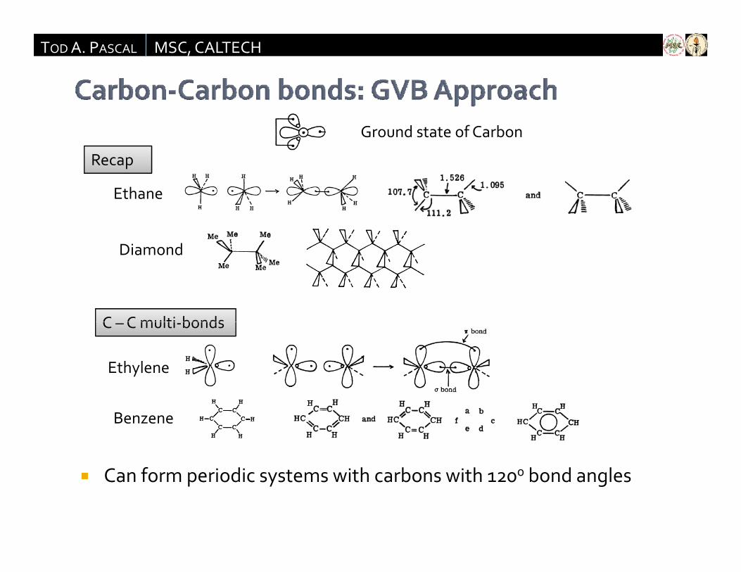
TODA. PASCAL MSC, CALTECH
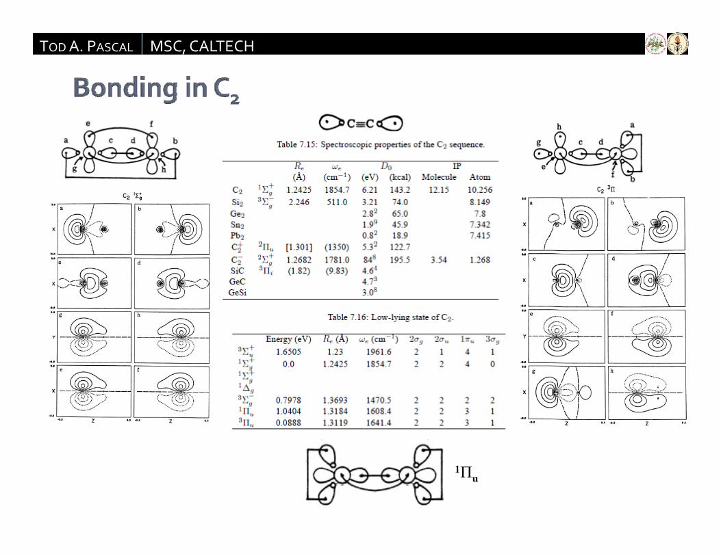
Recap
Ground state of Carbon
Ethane
DiamondDiamond
C C multi bondsC –C multi‐bonds
Ethylene
Benzene
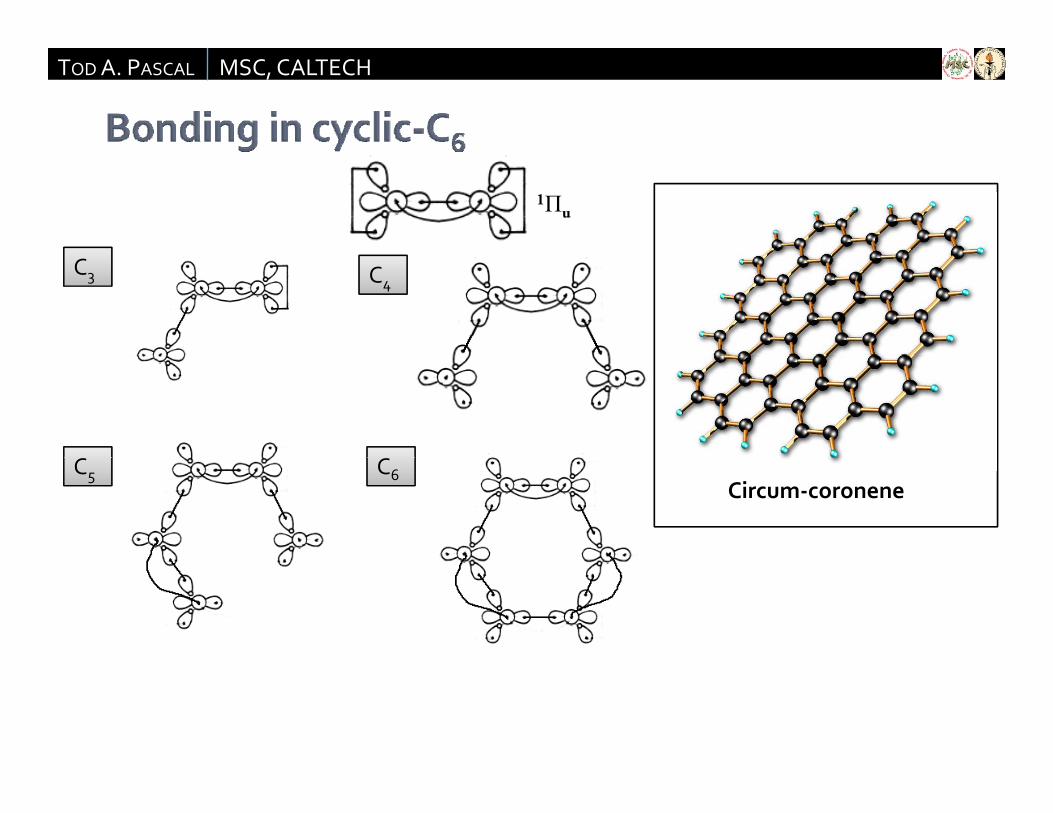
Can form periodic systems with carbons with 1200 bond angles
TODA. PASCAL MSC, CALTECH
1Πu
TODA. PASCAL MSC, CALTECH
1Πu
C3 C4
C5 C6Circum‐coronene
TODA. PASCAL MSC, CALTECH
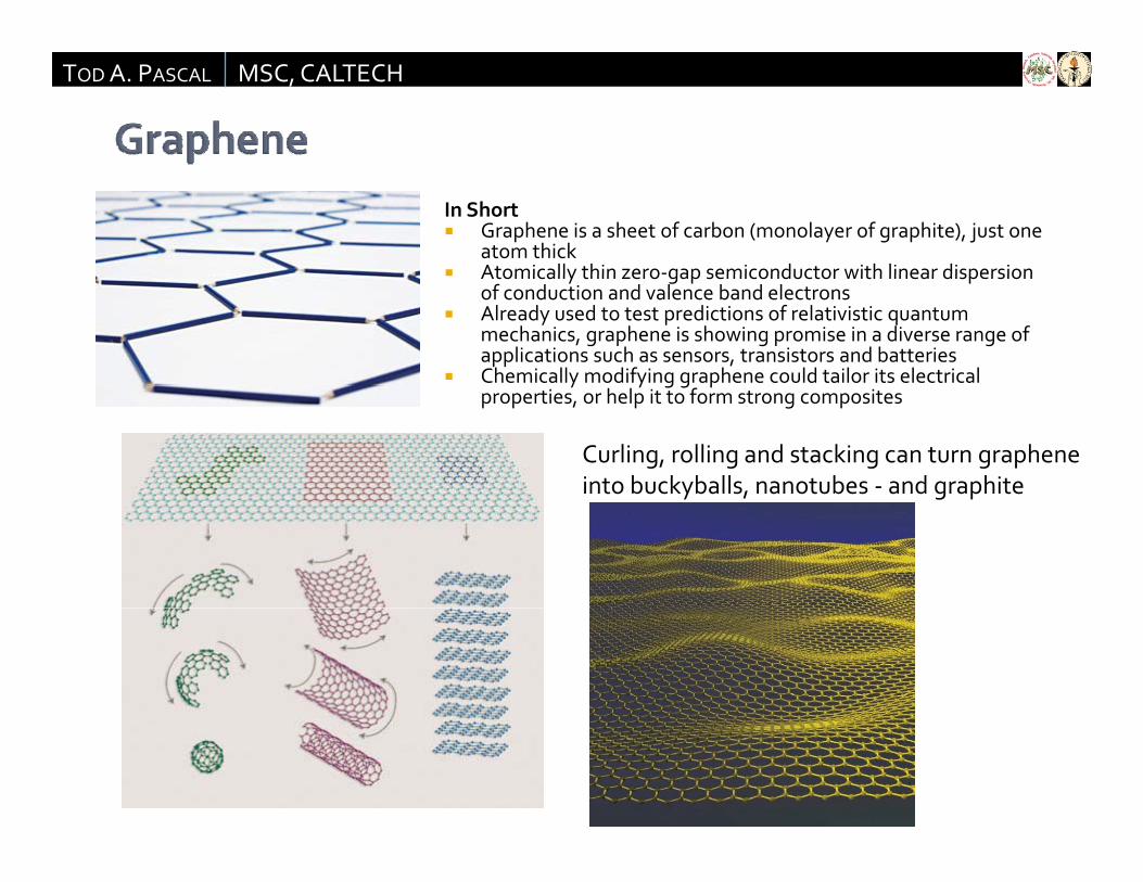
In Short Graphene is a sheet of carbon (monolayer of graphite), just one
atom thick Atomically thin zero‐gap semiconductor with linear dispersion Atomically thin zero gap semiconductor with linear dispersion
of conduction and valence band electrons Already used to test predictions of relativistic quantum
mechanics, graphene is showing promise in a diverse range of applications such as sensors, transistors and batteries
Chemically modifying graphene could tailor its electrical y y g g pproperties, or help it to form strong composites
Curling, rolling and stacking can turn grapheneinto buckyballs, nanotubes ‐ and graphitey , g p
TODA. PASCAL MSC, CALTECH
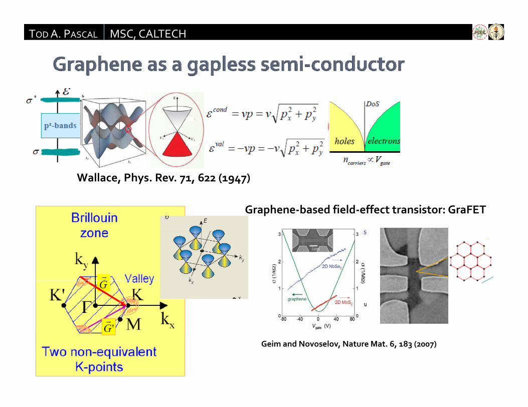
Wallace Phys Rev 71 622 (1947)Wallace, Phys. Rev. 71, 622 (1947)
Graphene‐based field‐effect transistor: GraFET
Geim and Novoselov, Nature Mat. 6, 183 (2007)
TODA. PASCAL MSC, CALTECH
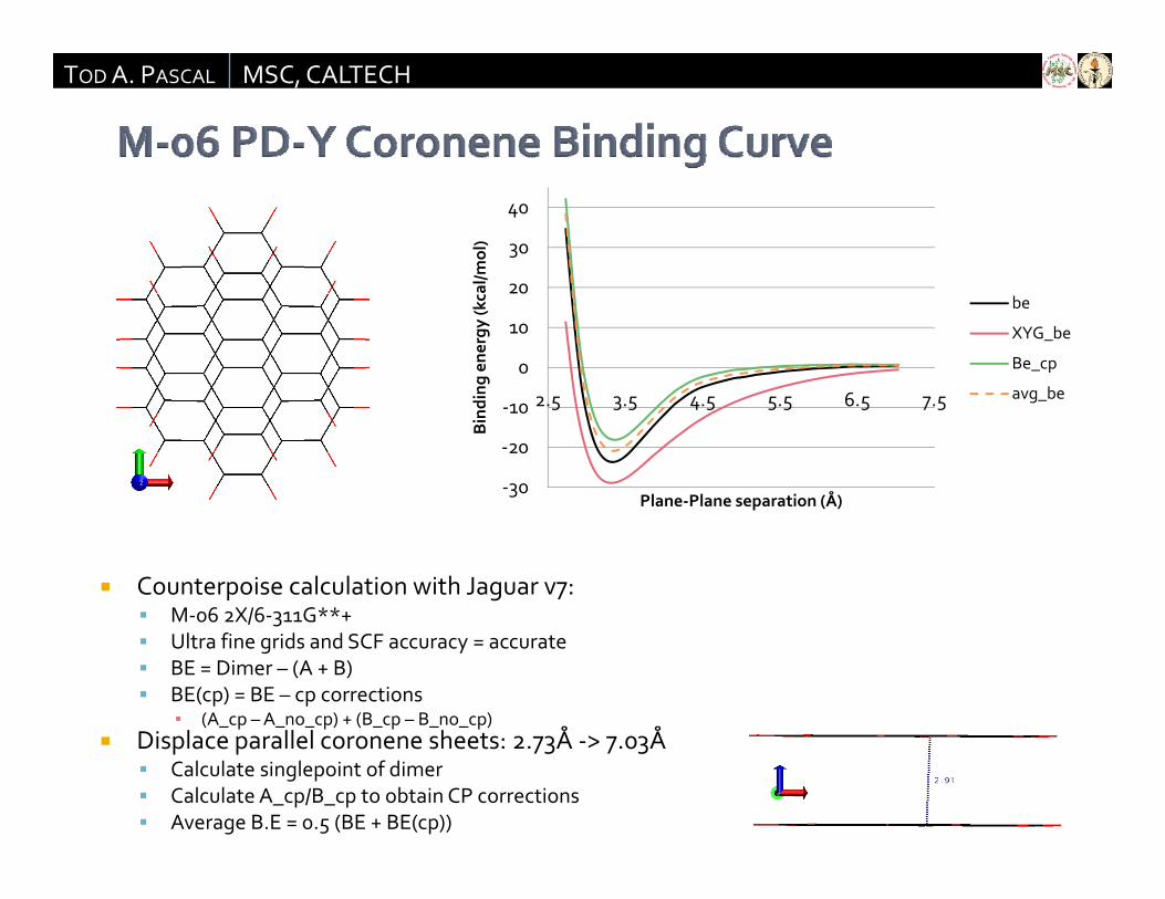
30
40
/mol)
0
10
20
6ng ene
rgy (kca
l/
be
XYG_be
Be_cp
avg be
‐30
‐20
‐10 2.5 3.5 4.5 5.5 6.5 7.5
Bindin
Plane‐Plane separation (Å)
avg_be
Counterpoise calculation with Jaguar v7: M‐06 2X/6‐311G**+
a e a e sepa at o ( )
M 06 2X/6 311G + Ultra fine grids and SCF accuracy = accurate BE = Dimer – (A + B) BE(cp) = BE – cp corrections
▪ (A_cp –A_no_cp) + (B_cp – B_no_cp)Di l ll l h t Å Å Displace parallel coronene sheets: 2.73Å ‐> 7.03Å Calculate singlepoint of dimer Calculate A_cp/B_cp to obtain CP corrections Average B.E = 0.5 (BE + BE(cp))
TODA. PASCAL MSC, CALTECH
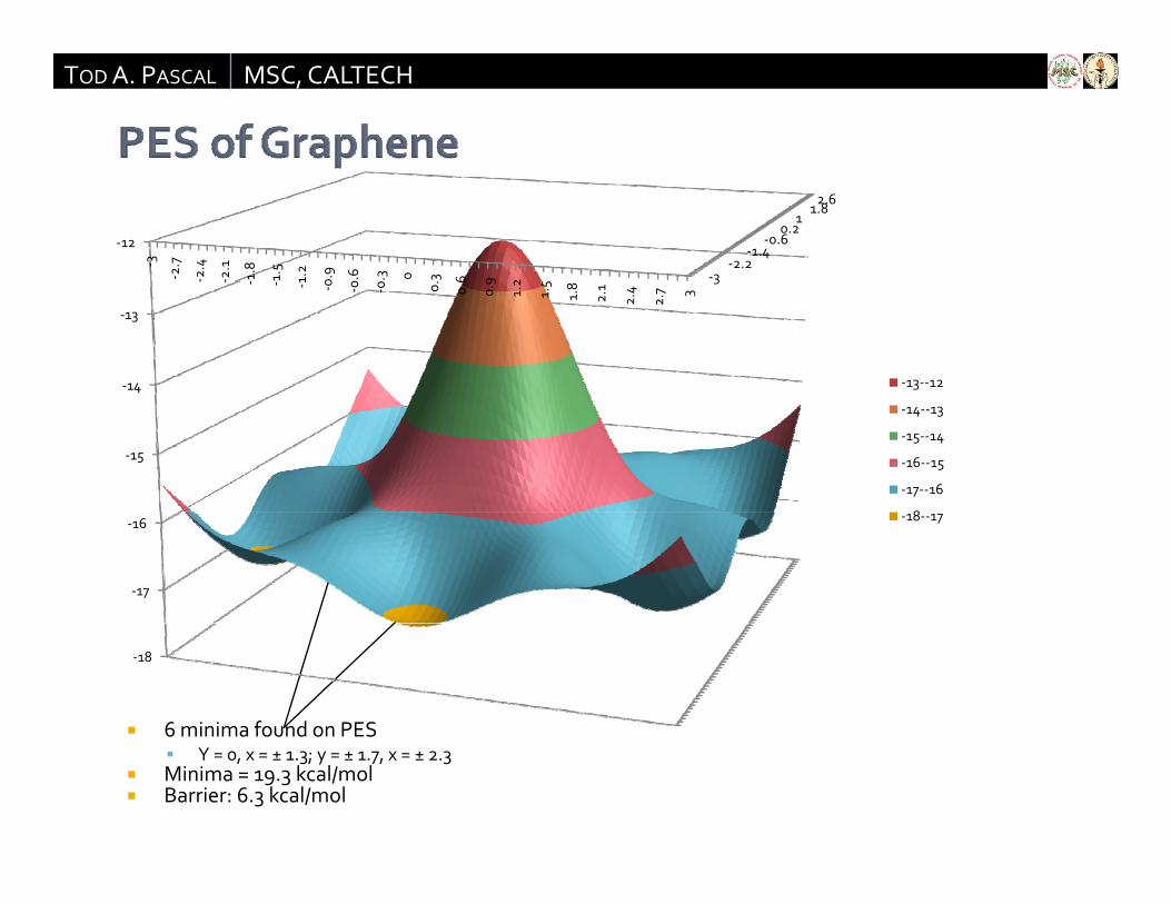
‐3‐2.2‐1.4‐0.6
0.21
1.82.6
‐12
‐3
‐2.7
‐2.4
‐2.1
‐1.8 1.5
1.2
0.9
0.6 .3 0 3 6 9 2 3
‐14
‐13
‐ ‐ ‐ ‐ ‐ 1 ‐0 ‐0 ‐0 0. 0.6
0.9
1.2
1.5
1.8
2.1
2.4
2.7 3
‐13‐‐12
‐15
‐14‐‐13
‐15‐‐14
‐16‐‐15
‐17‐‐16
‐17
‐16 ‐18‐‐17
6 minima found on PES
‐18
Y = 0, x = ± 1.3; y = ± 1.7, x = ± 2.3 Minima = 19.3 kcal/mol Barrier: 6.3 kcal/mol
TODA. PASCAL MSC, CALTECH
TODA. PASCAL MSC, CALTECH
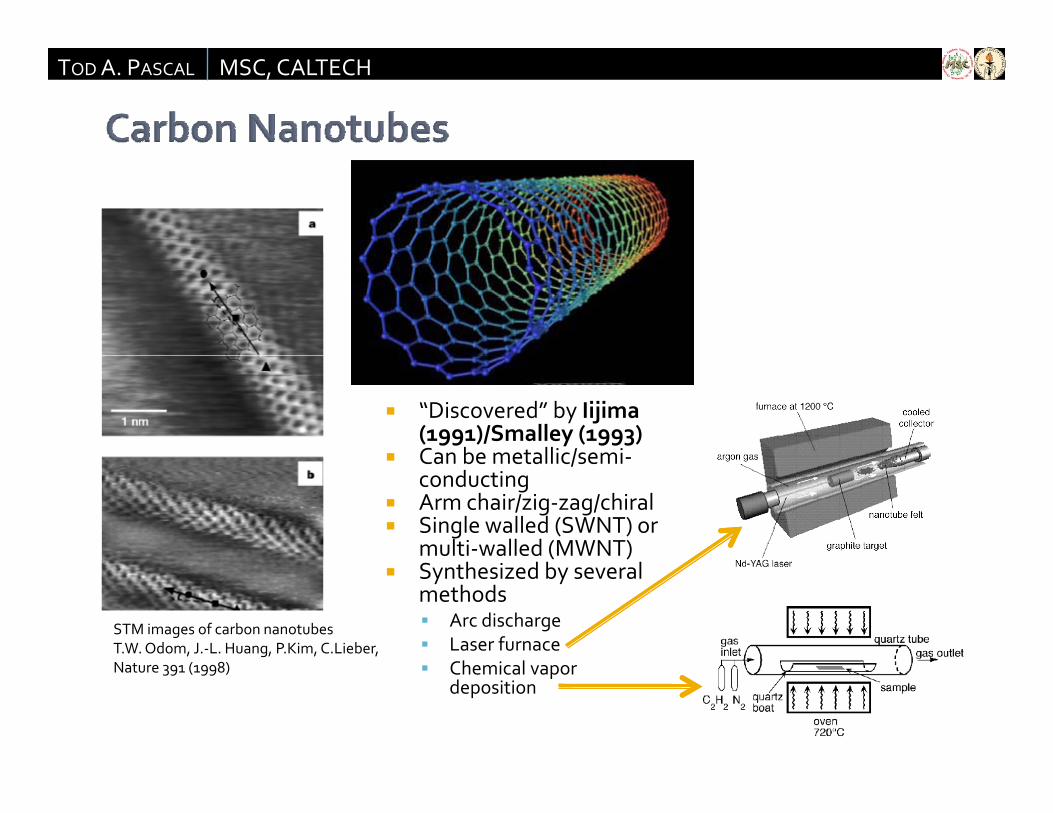
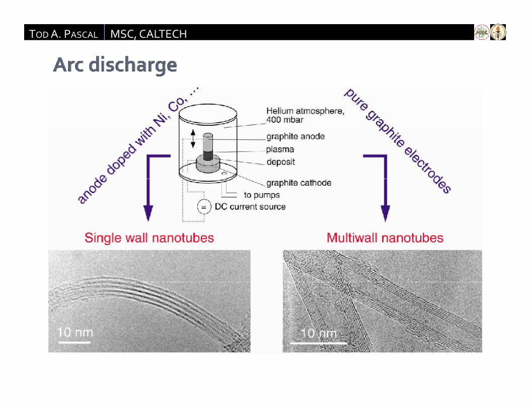
“Discovered” by Iijima(1991)/Smalley (1993)
Can be metallic/semi‐ Can be metallic/semi‐conducting
Arm chair/zig‐zag/chiral Single walled (SWNT) or
multi‐walled (MWNT) Synthesized by several
methods Arc discharge Laser furnace
Ch i l
STM images of carbon nanotubesT.W. Odom, J.‐L. Huang, P.Kim, C.Lieber, N t ( 8) Chemical vapor
depositionNature 391 (1998)
TODA. PASCAL MSC, CALTECH
TODA. PASCAL MSC, CALTECH
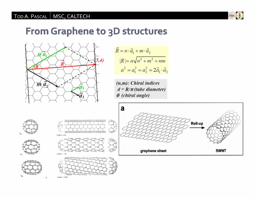
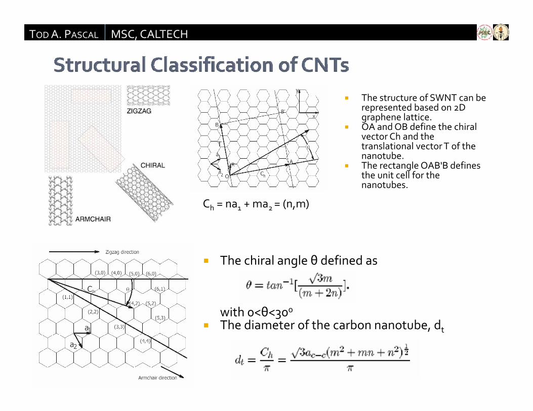
The structure of SWNT can be represented based on 2D graphene lattice.
OA and OB define the chiral OA and OB define the chiral vector Ch and the translational vector T of the nanotube.
The rectangle OAB'B defines the unit cell for the
Ch = na1 + ma2 = (n,m)
nanotubes.
The chiral angle θ defined as
with 0<θ<300
The diameter of the carbon nanotube, dt
TODA. PASCAL MSC, CALTECH
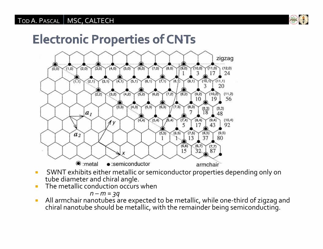
SWNT exhibits either metallic or semiconductor properties depending only on SWNT exhibits either metallic or semiconductor properties depending only on tube diameter and chiral angle.
The metallic conduction occurs whenn – m = 3q
All armchair nanotubes are expected to be metallic, while one‐third of zigzag and p , g gchiral nanotube should be metallic, with the remainder being semiconducting.
TODA. PASCAL MSC, CALTECH
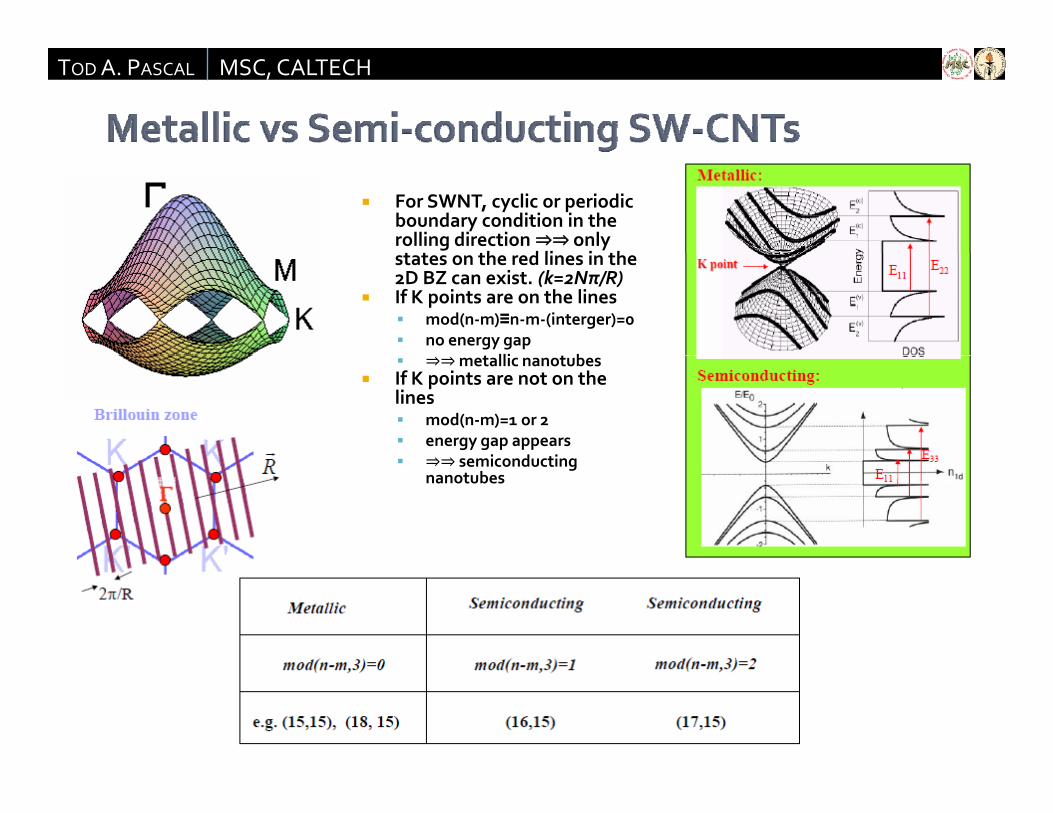
For SWNT, cyclic or periodic boundary condition in the rolling direction only t t th d li i th states on the red lines in the 2D BZ can exist. (k=2Nπ/R)
If K points are on the lines mod(n‐m)≡n‐m‐(interger)=0 no energy gap
lli b metallic nanotubes If K points are not on the
lines mod(n‐m)=1 or 2 energy gap appears
i d ti semiconducting nanotubes
TODA. PASCAL MSC, CALTECH
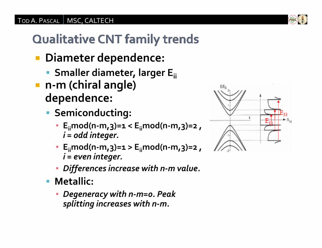
Diameter dependence: Smaller diameter, larger Eii, g ii
n‐m (chiral angle) dependence: Semiconducting:▪ Eiimod(n‐m,3)=1 < Eiimod(n‐m,3)=2 , i = odd integer.g
▪ Eiimod(n‐m,3)=1 > Eiimod(n‐m,3)=2 , i = even integer.
▪ Differences increase with n‐m value.Differences increase with n m value.
Metallic:▪ Degeneracy with n‐m=0. Peak splitting increases with n msplitting increases with n‐m.