CD4051B-Q1, CD4052B-Q1, CD4053B-Q1 CMOS … · cd4051b-q1, cd4052b-q1, cd4053b-q1 cmos analog...
24
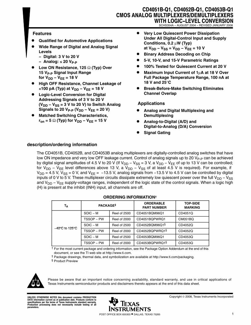
CD4051B-Q1, CD4052B-Q1, CD4053B-Q1 CMOS ANALOG MULTIPLEXERS/DEMULTIPLEXERS WITH LOGIC-LEVEL CONVERSION SCHS354A - AUGUST 2004 - REVISED JANUARY 2008 1 POST OFFICE BOX 655303 • DALLAS, TEXAS 75265 Features D Qualified for Automotive Applications D Wide Range of Digital and Analog Signal Levels - Digital: 3 V to 20 V - Analog: 3 20 V P-P D Low ON Resistance, 125 Ω (Typ) Over 15 V P-P Signal Input Range for V DD - V EE = 18 V D High OFF Resistance, Channel Leakage of +100 pA (Typ) at V DD - V EE = 18 V D Logic-Level Conversion for Digital Addressing Signals of 3 V to 20 V (V DD - V SS = 3 V to 20 V) to Switch Analog Signals to 20 V P-P (V DD - V EE = 20 V) D Matched Switching Characteristics, r on = 5 Ω (Typ) for V DD - V EE = 15 V D Very Low Quiescent Power Dissipation Under All Digital-Control Input and Supply Conditions, 0.2 µW (Typ) at V DD - V SS = V DD - V EE = 10 V D Binary Address Decoding on Chip D 5-V, 10-V, and 15-V Parametric Ratings D 100% Tested for Quiescent Current at 20 V D Maximum Input Current of 1µA at 18 V Over Full Package Temperature Range, 100 nA at 18 V and 25°C D Break-Before-Make Switching Eliminates Channel Overlap Applications D Analog and Digital Multiplexing and Demultiplexing D Analog-to-Digital (A/D) and Digital-to-Analog (D/A) Conversion D Signal Gating description/ordering information The CD4051B, CD4052B, and CD4053B analog multiplexers are digitally-controlled analog switches that have low ON impedance and very low OFF leakage current. Control of analog signals up to 20 V P-P can be achieved by digital signal amplitudes of 4.5 V to 20 V (If V DD - V SS = 3 V, a V DD - V EE of up to 13 V can be controlled; for V DD - V EE level differences above 13 V, a V DD - V SS of at least 4.5 V is required). For example, if V DD = 4.5 V, V SS = 0 V, and V EE = -13.5 V, analog signals from -13.5 V to 4.5 V can be controlled by digital inputs of 0 V to 5 V. These multiplexer circuits dissipate extremely low quiescent power over the full V DD - V SS and V DD - V EE supply-voltage ranges, independent of the logic state of the control signals. When a logic high (H) is present at the inhibit (INH) input, all channels are off. ORDERING INFORMATION † T A PACKAGE ‡ ORDERABLE PART NUMBER TOP-SIDE MARKING SOIC - M Reel of 2500 CD4051BQM96Q1 CD4051Q TSSOP - PW Reel of 2000 CD4051BQPWRQ1 CM051BQ 40°C to 125°C SOIC - M Reel of 2500 CD4052BQM96Q1 § CD4052Q -40°C to 125°C TSSOP - PW Reel of 2000 CD4052BQPWRQ1 § CD4052Q SOIC - M Reel of 2500 CD4053BQM96Q1 CD4053Q TSSOP - PW Reel of 2000 CD4053BQPWRQ1 § CD4053Q † For the most current package and ordering information, see the Package Option Addendum at the end of this document, or see the TI web site at http://www.ti.com. ‡ Package drawings, thermal data, and symbolization are available at http://www.ti.com/packaging. § Product Preview Copyright 2008, Texas Instruments Incorporated UNLESS OTHERWISE NOTED this document contains PRODUCTION DATA information current as of publication date. Products conform to specifications per the terms of Texas Instruments standard warranty. Production processing does not necessarily include testing of all parameters. Please be aware that an important notice concerning availability, standard warranty, and use in critical applications of Texas Instruments semiconductor products and disclaimers thereto appears at the end of this data sheet.
Transcript of CD4051B-Q1, CD4052B-Q1, CD4053B-Q1 CMOS … · cd4051b-q1, cd4052b-q1, cd4053b-q1 cmos analog...
CD4051B-Q1, CD4052B-Q1, CD4053B-Q1CMOS ANALOG MULTIPLEXERS/DEMULTIPLEXERS
WITH LOGIC−LEVEL CONVERSIONSCHS354A − AUGUST 2004 − REVISED JANUARY 2008
1POST OFFICE BOX 655303 • DALLAS, TEXAS 75265
Features
Qualified for Automotive Applications
Wide Range of Digital and Analog SignalLevels− Digital: 3 V to 20 V− Analog: 20 VP-P
Low ON Resistance, 125 Ω (Typ) Over 15 VP-P Signal Input Range for VDD − VEE = 18 V
High OFF Resistance, Channel Leakage of100 pA (Typ) at VDD − VEE = 18 V
Logic-Level Conversion for DigitalAddressing Signals of 3 V to 20 V (VDD − VSS = 3 V to 20 V) to Switch AnalogSignals to 20 VP-P (VDD − VEE = 20 V)
Matched Switching Characteristics, ron = 5 Ω (Typ) for VDD − VEE = 15 V
Very Low Quiescent Power DissipationUnder All Digital-Control Input and SupplyConditions, 0.2 µW (Typ) at VDD − VSS = VDD − VEE = 10 V
Binary Address Decoding on Chip
5-V, 10-V, and 15-V Parametric Ratings
100% Tested for Quiescent Current at 20 V
Maximum Input Current of 1µA at 18 V OverFull Package Temperature Range, 100 nA at18 V and 25°C
Break-Before-Make Switching EliminatesChannel Overlap
Applications
Analog and Digital Multiplexing andDemultiplexing
Analog-to-Digital (A/D) andDigital-to-Analog (D/A) Conversion
Signal Gating
description/ordering information
The CD4051B, CD4052B, and CD4053B analog multiplexers are digitally-controlled analog switches that havelow ON impedance and very low OFF leakage current. Control of analog signals up to 20 VP-P can be achievedby digital signal amplitudes of 4.5 V to 20 V (If VDD − VSS = 3 V, a VDD − VEE of up to 13 V can be controlled;for VDD − VEE level differences above 13 V, a VDD − VSS of at least 4.5 V is required). For example, if VDD = 4.5 V, VSS = 0 V, and VEE = −13.5 V, analog signals from −13.5 V to 4.5 V can be controlled by digitalinputs of 0 V to 5 V. These multiplexer circuits dissipate extremely low quiescent power over the full VDD − VSSand VDD − VEE supply-voltage ranges, independent of the logic state of the control signals. When a logic high(H) is present at the inhibit (INH) input, all channels are off.
ORDERING INFORMATION†
TA PACKAGE‡ ORDERABLEPART NUMBER
TOP-SIDEMARKING
SOIC − M Reel of 2500 CD4051BQM96Q1 CD4051Q
TSSOP − PW Reel of 2000 CD4051BQPWRQ1 CM051BQ
40°C to 125°CSOIC − M Reel of 2500 CD4052BQM96Q1§ CD4052Q
−40°C to 125°CTSSOP − PW Reel of 2000 CD4052BQPWRQ1§ CD4052Q
SOIC − M Reel of 2500 CD4053BQM96Q1 CD4053Q
TSSOP − PW Reel of 2000 CD4053BQPWRQ1§ CD4053Q
† For the most current package and ordering information, see the Package Option Addendum at the end of thisdocument, or see the TI web site at http://www.ti.com.
‡ Package drawings, thermal data, and symbolization are available at http://www.ti.com/packaging.§ Product Preview
Copyright 2008, Texas Instruments IncorporatedUNLESS OTHERWISE NOTED this document contains PRODUCTIONDATA information current as of publication date. Products conform tospecifications per the terms of Texas Instruments standard warranty.Production processing does not necessarily include testing of allparameters.
Please be aware that an important notice concerning availability, standard warranty, and use in critical applications ofTexas Instruments semiconductor products and disclaimers thereto appears at the end of this data sheet.
CD4051B-Q1, CD4052B-Q1, CD4053B-Q1CMOS ANALOG MULTIPLEXERS/DEMULTIPLEXERSWITH LOGIC−LEVEL CONVERSIONSCHS354A − AUGUST 2004 − REVISED JANUARY 2008
2 POST OFFICE BOX 655303 • DALLAS, TEXAS 75265
description/ordering information (continued)
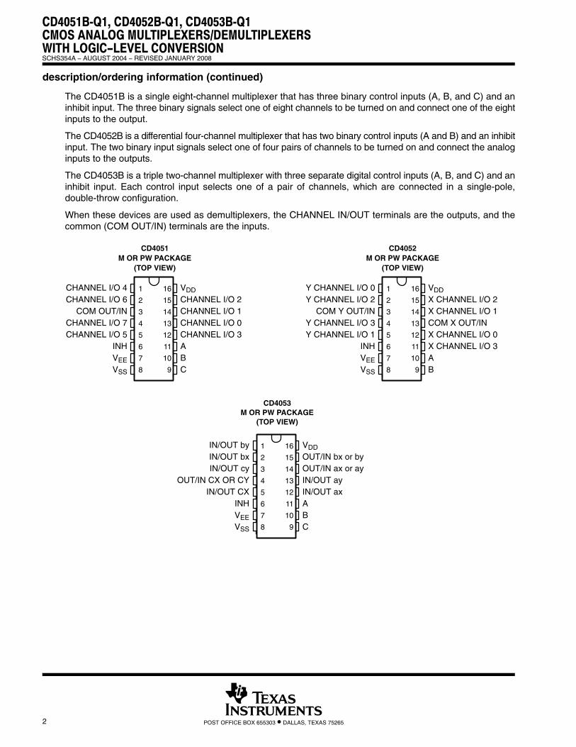
The CD4051B is a single eight-channel multiplexer that has three binary control inputs (A, B, and C) and aninhibit input. The three binary signals select one of eight channels to be turned on and connect one of the eightinputs to the output.
The CD4052B is a differential four-channel multiplexer that has two binary control inputs (A and B) and an inhibitinput. The two binary input signals select one of four pairs of channels to be turned on and connect the analoginputs to the outputs.
The CD4053B is a triple two-channel multiplexer with three separate digital control inputs (A, B, and C) and aninhibit input. Each control input selects one of a pair of channels, which are connected in a single-pole,double-throw configuration.
When these devices are used as demultiplexers, the CHANNEL IN/OUT terminals are the outputs, and thecommon (COM OUT/IN) terminals are the inputs.
CD4053M OR PW PACKAGE
(TOP VIEW)
1
2
3
4
5
6
7
8
16
15
14
13
12
11
10
9
IN/OUT byIN/OUT bxIN/OUT cy
OUT/IN CX OR CYIN/OUT CX
INHVEE
VSS
VDD
OUT/IN bx or byOUT/IN ax or ayIN/OUT ayIN/OUT axABC
CD4051M OR PW PACKAGE
(TOP VIEW)
1
2
3
4
5
6
7
8
16
15
14
13
12
11
10
9
CHANNEL I/O 4CHANNEL I/O 6
COM OUT/INCHANNEL I/O 7CHANNEL I/O 5
INHVEE
VSS
VDD
CHANNEL I/O 2CHANNEL I/O 1CHANNEL I/O 0CHANNEL I/O 3ABC
CD4052M OR PW PACKAGE
(TOP VIEW)
1
2
3
4
5
6
7
8
16
15
14
13
12
11
10
9
Y CHANNEL I/O 0Y CHANNEL I/O 2
COM Y OUT/INY CHANNEL I/O 3Y CHANNEL I/O 1
INHVEE
VSS
VDD
X CHANNEL I/O 2X CHANNEL I/O 1COM X OUT/INX CHANNEL I/O 0X CHANNEL I/O 3AB
CD4051B-Q1, CD4052B-Q1, CD4053B-Q1CMOS ANALOG MULTIPLEXERS/DEMULTIPLEXERS
WITH LOGIC−LEVEL CONVERSIONSCHS354A − AUGUST 2004 − REVISED JANUARY 2008
3POST OFFICE BOX 655303 • DALLAS, TEXAS 75265
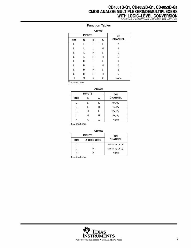
Function Tables
CD4051
INPUTS ONINH C B A
ONCHANNEL
L L L L 0
L L L H 1
L L H L 2
L L H H 3
L H L L 4
L H L H 5
L H H L 6
L H H H 7
H X X X None
X = don’t care
CD4052
INPUTS ONINH B A
ONCHANNEL
L L L 0x, 0y
L L H 1x, 2y
L H L 2x, 2y
L H H 3x, 3y
H X X None
X = don’t care
CD4053
INPUTS ONINH A OR B OR C
ONCHANNEL
L L ax or bx or cx
L H ay or by or cy
H X None
X = don’t care
CD4051B-Q1, CD4052B-Q1, CD4053B-Q1CMOS ANALOG MULTIPLEXERS/DEMULTIPLEXERSWITH LOGIC−LEVEL CONVERSIONSCHS354A − AUGUST 2004 − REVISED JANUARY 2008
4 POST OFFICE BOX 655303 • DALLAS, TEXAS 75265
logic diagram (positive logic)
† All inputs are protected by CMOS protection network.
11
10
9
6
A
B
C
INH
134 2 5 1 12 15 14
TG
TG
TG
TG
TG
TG
TG
TG
3 COMOUT/IN
01234567
8 7
16
CHANNEL I/O
†
†
†
†
CD4051B
Logic-LevelConversion
Binaryto
1-of-8Decoder
WithInhibit
VDD
VSS VEE
† All inputs are protected by CMOS protection network.
CD4052B
1211 15 14
0123
3210
X CHANNEL I/O
Y CHANNEL I/O
13
3
78
16
6
9
10A
B
INH
TG
TG
TG
TG
TG
TG
TG
TG
4251
Binaryto
1-of-4Decoder
WithInhibit
†
†
†
COM XOUT/IN
Logic-LevelConversion
VDD
VSS VEE
COM YOUT/IN

CD4051B-Q1, CD4052B-Q1, CD4053B-Q1CMOS ANALOG MULTIPLEXERS/DEMULTIPLEXERS
WITH LOGIC−LEVEL CONVERSIONSCHS354A − AUGUST 2004 − REVISED JANUARY 2008
5POST OFFICE BOX 655303 • DALLAS, TEXAS 75265
logic diagrams (positive logic) (continued)
11
10
9
6
A†
B†
C†
INH†
123 5 1 2 13
TG
TG
TG
TG
TG
TG
4
axaybxbycxcy
8 7
16IN/OUT
15
14
VDD
† All inputs are protected by standard CMOS protection network.
CD4053B
Logic-LevelConversion
VDD
VSS VEE
Binary to1-of-2
DecodersWith
Inhibit
COM OUT/INac or ay
COM OUT/INbc or by
COM OUT/INxc or xy
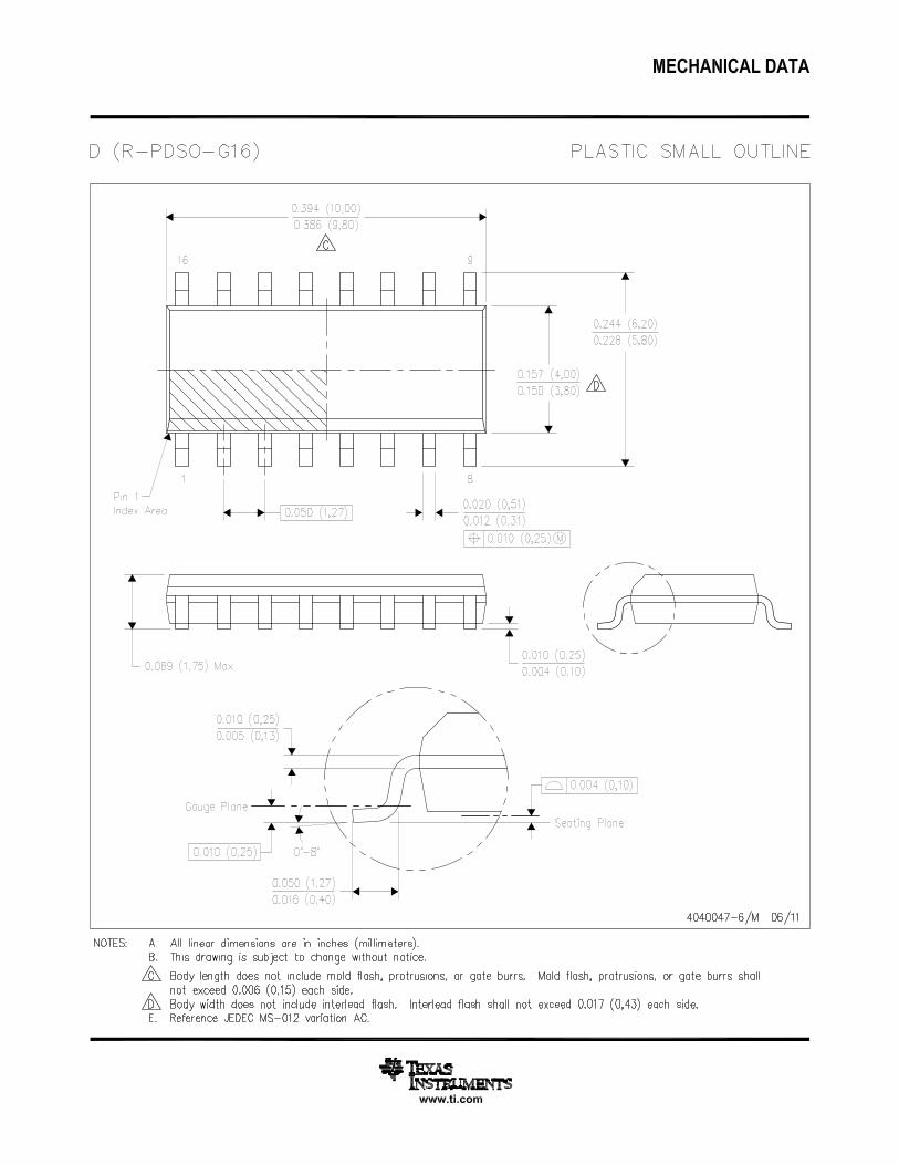
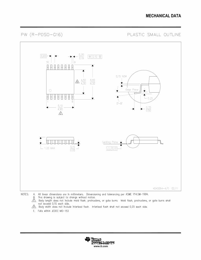
absolute maximum ratings over operating free-air temperature (unless otherwise noted)‡
Supply voltage range, V+ to V− (voltages referenced to VSS terminal) −0.5 to 20 V. . . . . . . . . . . . . . . . . . . . . . DC input voltage range −0.5 V to VDD + 0.5 V. . . . . . . . . . . . . . . . . . . . . . . . . . . . . . . . . . . . . . . . . . . . . . . . . . . . . . DC input current, any one input ±10 mA. . . . . . . . . . . . . . . . . . . . . . . . . . . . . . . . . . . . . . . . . . . . . . . . . . . . . . . . . . . Package thermal impedance, θJA (see Note 1): M package 73°C/W. . . . . . . . . . . . . . . . . . . . . . . . . . . . . . . . . .
PW package 108°C/W. . . . . . . . . . . . . . . . . . . . . . . . . . . . . . . . Maximum junction temperature, TJ 150°C. . . . . . . . . . . . . . . . . . . . . . . . . . . . . . . . . . . . . . . . . . . . . . . . . . . . . . . . . Lead temperature (during soldering):
At distance 1/16 ± 1/32 inch (1,59 ± 0,79 mm) from case for 10 s max 265°C. . . . . . . . . . . . . . . . . . . . . . . Storage temperature range, Tstg −65°C to 150°C. . . . . . . . . . . . . . . . . . . . . . . . . . . . . . . . . . . . . . . . . . . . . . . . . . .
‡ Stresses beyond those listed under “absolute maximum ratings” may cause permanent damage to the device. These are stress ratings only, andfunctional operation of the device at these or any other conditions beyond those indicated under “recommended operating conditions” is notimplied. Exposure to absolute-maximum-rated conditions for extended periods may affect device reliability.
NOTE 1: The package thermal impedance is calculated in accordance with JESD 51-7.
CD4051B-Q1, CD4052B-Q1, CD4053B-Q1CMOS ANALOG MULTIPLEXERS/DEMULTIPLEXERSWITH LOGIC−LEVEL CONVERSIONSCHS354A − AUGUST 2004 − REVISED JANUARY 2008
6 POST OFFICE BOX 655303 • DALLAS, TEXAS 75265
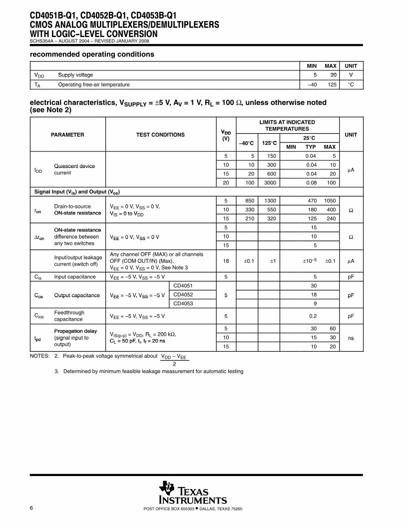
recommended operating conditions
MIN MAX UNIT
V Supply voltage 5 20 VVDD Supply voltage 5 20 V
TA Operating free-air temperature −40 125 °C
electrical characteristics, VSUPPLY = ±5 V, AV = 1 V, RL = 100 Ω, unless otherwise noted (see Note 2)
PARAMETER TEST CONDITIONS VDD
LIMITS AT INDICATEDTEMPERATURES
UNITPARAMETER TEST CONDITIONS VDD(V)
40°C 125°C25°C UNIT
(V)−40°C 125°C
MIN TYP MAX
5 5 150 0.04 5
IQuiescent device 10 10 300 0.04 10
AIDDQuiescent devicecurrent 15 20 600 0.04 20
µA
20 100 3000 0.08 100
Signal Input (Vis) and Output (Vos)
D i t V 0 V V 0 V5 850 1300 470 1050
ronDrain-to-sourceON-state resistance
VEE = 0 V, VSS = 0 V,VIS = 0 to VDD
10 330 550 180 400 Ωron ON-state resistance VIS = 0 to VDD15 210 320 125 240
Ω
ON-state resistance 5 15
∆ron
ON-state resistancedifference between VEE = 0 V, VSS = 0 V 10 10 Ω∆ron difference betweenany two switches
VEE 0 V, VSS 0 V
15 5
Ω
Input/output leakagecurrent (switch off)
Any channel OFF (MAX) or all channelsOFF (COM OUT/IN) (Max), VEE = 0 V, VSS = 0 V, See Note 3
18 ±0.1 ±1 ±10−5 ±0.1 µA
Cis Input capacitance VEE = −5 V, VSS = −5 V 5 5 pF
CD4051 30
Cos Output capacitance VEE = −5 V, VSS = −5 V CD4052 5 18 pFCos Output capacitance VEE 5 V, VSS 5 V
CD4053
5
9
pF
CiosFeedthroughcapacitance
VEE = −5 V, VSS = −5 V 5 0.2 pF
Propagation delayV V R 200 kΩ
5 30 60
tpd
Propagation delay(signal input to
VIS(p-p) = VDD, RL = 200 kΩ, CL = 50 pF tr tf = 20 ns
10 15 30 nstpd (signal input tooutput)
CL = 50 pF, tr, tf = 20 ns15 10 20
ns
NOTES: 2. Peak-to-peak voltage symmetrical about VDD − VEE
23. Determined by minimum feasible leakage measurement for automatic testing
CD4051B-Q1, CD4052B-Q1, CD4053B-Q1CMOS ANALOG MULTIPLEXERS/DEMULTIPLEXERS
WITH LOGIC−LEVEL CONVERSIONSCHS354A − AUGUST 2004 − REVISED JANUARY 2008
7POST OFFICE BOX 655303 • DALLAS, TEXAS 75265
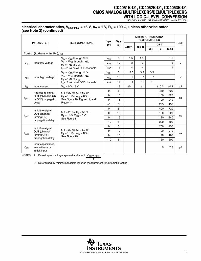
electrical characteristics, VSUPPLY = ±5 V, AV = 1 V, RL = 100 Ω, unless otherwise noted (see Note 2) (continued)
PARAMETER TEST CONDITIONS VEE VDD
LIMITS AT INDICATEDTEMPERATURES
UNITPARAMETER TEST CONDITIONS VEE(V)
VDD(V)
40°C 125°C25°C UNIT
(V) (V)−40°C 125°C
MIN TYP MAX
Control (Address or Inhibit), VC
VIL = VDD through 1kΩ, VSS 5 1.5 1.5 1.5
VIL Input low voltage
IL DD g ,VIH = VDD through 1kΩ,RL = 1kΩ to VSS
VSS 10 3 3 3 VIL p gRL = 1kΩ to VSS, Iis < 2 µA on all OFF channels VSS 15 4 4 4
VIL = VDD through 1kΩ, VSS 5 3.5 3.5 3.5
VIH Input high voltage
IL DD g ,VIH = VDD through 1kΩ,RL = 1kΩ to VSS
VSS 10 7 7 7 VIH p g gRL = 1kΩ to VSS, Iis < 2 µA on all OFF channels VSS 15 11 11 11
IIN Input current VIN = 0 V, 18 V 18 ±0.1 ±1 ±10−5 ±0.1 µA
Address-to-signal t tf = 20 ns CL = 50 pF0 5 450 720
t
Address-to-signalOUT (channels ON
tr, tf = 20 ns, CL = 50 pF,RL = 10 kΩ, VSS = 0 V, 0 10 160 320
nstpd1OUT (channels ONor OFF) propagationd l
RL = 10 kΩ, VSS = 0 V,See Figure 10, Figure 11, andFi 14
0 15 120 240ns) p p g
delayg g
Figure 14−5 5 225 450
Inhibit-to-signal0 5 400 720
t
Inhibit-to-signalOUT (channel
tr, tf = 20 ns, CL = 50 pF,R 1 kΩ V 0 V
0 10 160 320nstpd2
OUT (channelturning ON)
ti d l
RL = 1 kΩ, VSS = 0 V,See Figure 11 0 15 120 240
nsg )propagation delay
See Figure 11−10 5 200 400
Inhibit-to-signal0 5 200 450
t
Inhibit-to-signalOUT (channel
tr, tf = 20 ns, CL = 50 pF,R 10 kΩ V 0 V
0 10 90 210nstpd3
OUT (channelturning OFF)
ti d l
RL = 10 kΩ, VSS = 0 V,See Figure 15 0 15 70 160
nsg )propagation delay
See Figure 15−10 5 130 300
CIN
Input capacitance,any address orinhibit input
5 7.5 pF
NOTES: 2: Peak-to-peak voltage symmetrical about VDD − VEE
23: Determined by minimum feasible leakage measurement for automatic testing
CD4051B-Q1, CD4052B-Q1, CD4053B-Q1CMOS ANALOG MULTIPLEXERS/DEMULTIPLEXERSWITH LOGIC−LEVEL CONVERSIONSCHS354A − AUGUST 2004 − REVISED JANUARY 2008
8 POST OFFICE BOX 655303 • DALLAS, TEXAS 75265
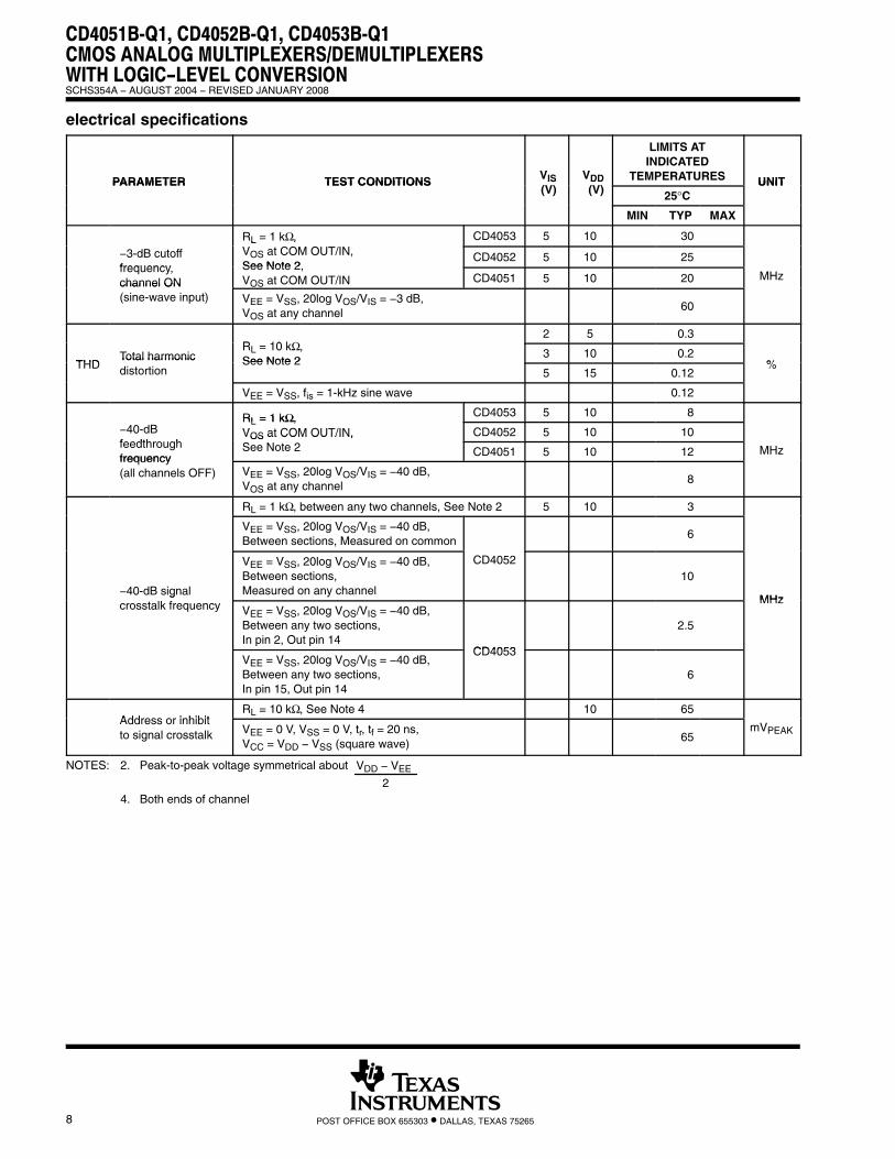
electrical specifications
PARAMETER TEST CONDITIONS VIS(V)
VDD(V)
LIMITS ATINDICATED
TEMPERATURES UNITPARAMETER TEST CONDITIONS IS(V)
DD(V) 25°C
UNIT
MIN TYP MAX
RL = 1 kΩ, CD4053 5 10 30
−3-dB cutofffrequency
L ,VOS at COM OUT/IN, See Note 2
CD4052 5 10 25frequency,channel ON
See Note 2, VOS at COM OUT/IN CD4051 5 10 20 MHzchannel ON
(sine-wave input) VEE = VSS, 20log VOS/VIS = −3 dB,VOS at any channel
60
R 10 kΩ2 5 0.3
THDTotal harmonic
RL = 10 kΩ, See Note 2
3 10 0.2%THD
Total harmonicdistortion
See Note 25 15 0.12
%
VEE = VSS, fis = 1-kHz sine wave 0.12
RL = 1 kΩ, CD4053 5 10 8−40-dBf dth h
RL = 1 kΩ, VOS at COM OUT/IN, CD4052 5 10 10
feedthroughfrequency
VOS at COM OUT/IN, See Note 2 CD4051 5 10 12 MHz
frequency(all channels OFF) VEE = VSS, 20log VOS/VIS = −40 dB,
VOS at any channel8
RL = 1 kΩ, between any two channels, See Note 2 5 10 3
VEE = VSS, 20log VOS/VIS = −40 dB,Between sections, Measured on common
6
−40-dB signal
VEE = VSS, 20log VOS/VIS = −40 dB,Between sections,Measured on any channel
CD405210
MHzg
crosstalk frequency VEE = VSS, 20log VOS/VIS = −40 dB,Between any two sections,In pin 2, Out pin 14
CD4053
2.5
MHz
VEE = VSS, 20log VOS/VIS = −40 dB,Between any two sections,In pin 15, Out pin 14
CD4053
6
Address or inhibitRL = 10 kΩ, See Note 4 10 65
Address or inhibit to signal crosstalk VEE = 0 V, VSS = 0 V, tr, tf = 20 ns,
VCC = VDD − VSS (square wave)65
mVPEAK
NOTES: 2. Peak-to-peak voltage symmetrical about VDD − VEE
24. Both ends of channel
CD4051B-Q1, CD4052B-Q1, CD4053B-Q1CMOS ANALOG MULTIPLEXERS/DEMULTIPLEXERS
WITH LOGIC−LEVEL CONVERSIONSCHS354A − AUGUST 2004 − REVISED JANUARY 2008
9POST OFFICE BOX 655303 • DALLAS, TEXAS 75265
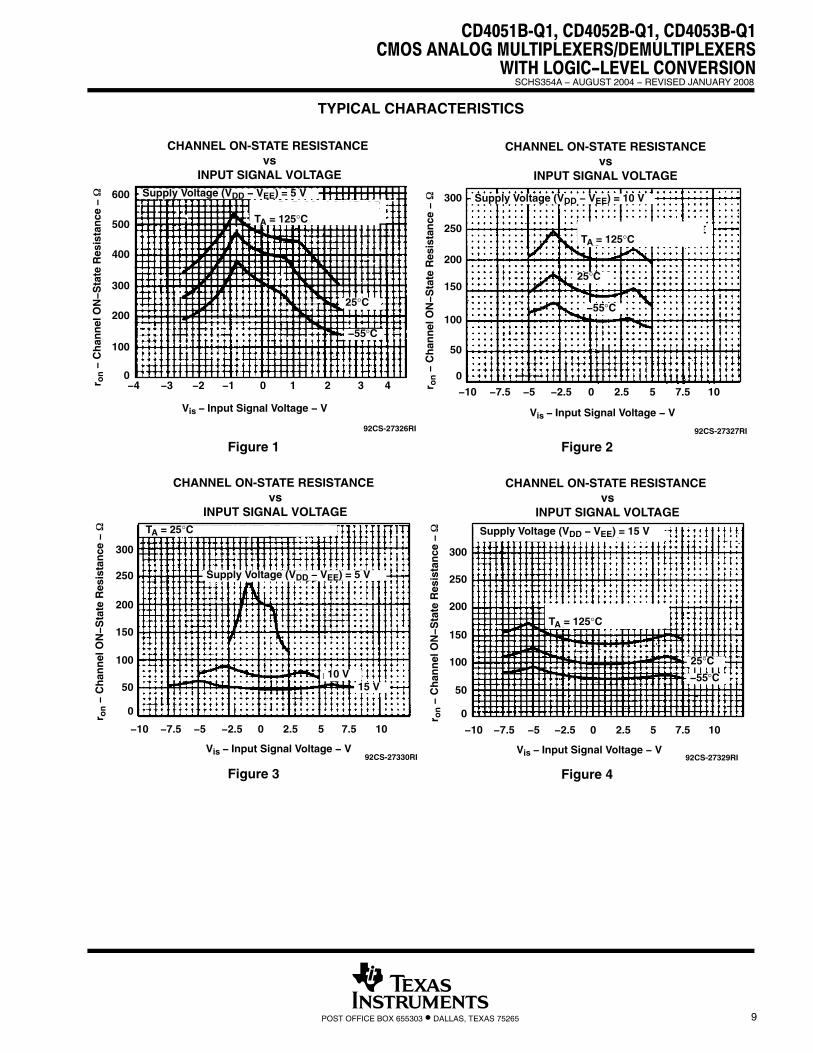
TYPICAL CHARACTERISTICS
Vis − Input Signal Voltage − V
600
500
400
300
200
100
0−4 −3 −2 −1 0 1 2 3 4
CHANNEL ON-STATE RESISTANCE vs
INPUT SIGNAL VOLTAGE
92CS-27326RI
Figure 1
TA = 125°C
25°C
−55°C
Supply Voltage (VDD − VEE) = 5 V
r on −
Ch
ann
el O
N−S
tate
Res
ista
nce
−
Figure 2
CHANNEL ON-STATE RESISTANCEvs
INPUT SIGNAL VOLTAGE
300
250
200
150
100
50
0
−10 −7.5 −5 −2.5 0 2.5 5 7.5 10
Supply Voltage (VDD − VEE) = 10 V
TA = 125°C
Vis − Input Signal Voltage − V
25°C
−55°C
92CS-27327RIr o
n −
Ch
ann
el O
N−S
tate
Res
ista
nce
−
Vis − Input Signal Voltage − V
Figure 3
CHANNEL ON-STATE RESISTANCE vs
INPUT SIGNAL VOLTAGE
300
250
200
150
100
50
0
−10 −7.5 −5 −2.5 0 2.5 5 7.5 10
Supply Voltage (VDD − VEE) = 5 V
TA = 25°C
10 V15 V
92CS-27330RI
r on −
Ch
ann
el O
N−S
tate
Res
ista
nce
−
Vis − Input Signal Voltage − V
CHANNEL ON-STATE RESISTANCE vs
INPUT SIGNAL VOLTAGE
Figure 4
300
250
200
150
100
50
0
−10 −7.5 −5 −2.5 0 2.5 5 7.5 10
Supply Voltage (VDD − VEE) = 15 V
TA = 125°C
25°C−55°C
92CS-27329RI
r on −
Ch
ann
el O
N−S
tate
Res
ista
nce
−
CD4051B-Q1, CD4052B-Q1, CD4053B-Q1CMOS ANALOG MULTIPLEXERS/DEMULTIPLEXERSWITH LOGIC−LEVEL CONVERSIONSCHS354A − AUGUST 2004 − REVISED JANUARY 2008
10 POST OFFICE BOX 655303 • DALLAS, TEXAS 75265
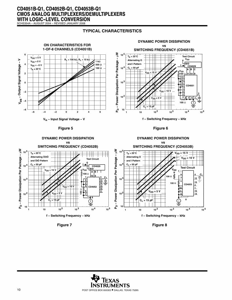
TYPICAL CHARACTERISTICS
Figure 5
ON CHARACTERISTICS FOR1-OF-8 CHANNELS (CD4051B)
Vis − Input Signal Voltage − V
Ou
tpu
t S
ign
al V
olt
age
− V
V
−o
s
−6 −4 −2 0 2 4 6−6
−4
−2
0
2
4
6VDD = 5 V
VSS = 0 V
VEE = −5 V
TA = 25C
RL = 100 k, RL = 10 k1 k500
100
Figure 6
f − Switching Frequency − kHz
DYNAMIC POWER DISSIPATIONvs
SWITCHING FREQUENCY (CD4051B)
10 510 410 310 10 2
10 2
10
10 3
10 4
10 5
1
Test Circuit
35
1011
678
1415
1
2
13
12
4 CL
CD4051
f
100 Ω
100 Ω
B/DCD4029A B C
9
Ι
TA = 25C
Alternating O
and I Pattern
CL = 50 pF
VDD = 10 V
VDD = 5 V
CL = 15 pF
VDD = 15 V
VDD
VDD
PD
− P
ow
er D
issi
pat
ion
Per
Pac
kag
e −
W
Figure 7
f − Switching Frequency − kHz
DYNAMIC POWER DISSIPATIONvs
SWITCHING FREQUENCY (CD4052B)
10 510 410 310 10 2
10 2
10
10 3
10 4
10 5
1
35
10
1167
8
1415
1
21312
4
CL
CD4052
f
100 Ω
100
Ω
B/DCD4029
A B
9
Ι
Test Circuit
PD
− P
ow
er D
issi
pat
ion
Per
Pac
kag
e −
W
TA = 25C
Alternating ÒOÓ
and ÒIÓ Pattern
CL = 50 pF
VDD = 10 V
VDD = 5 V
CL = 15 pF
VDD = 15 V VDD
Figure 8
f − Switching Frequency − kHz
DYNAMIC POWER DISSIPATIONvs
SWITCHING FREQUENCY (CD4053B)
10 510 410 310 10 2
10 2
10
10 3
10 4
10 5
1
VDD = 15 V
VDD = 10 V
VDD = 5 V
CL = 15 pF Ι
Test CircuitVDD
93
5
1011
67
8
14151213
12
4 CL
CD4053
f
100
100
PD
− P
ow
er D
issi
pat
ion
Per
Pac
kag
e −
W
TA = 25C
Alternating O
and I Pattern
CL = 50 pF
CD4051B-Q1, CD4052B-Q1, CD4053B-Q1CMOS ANALOG MULTIPLEXERS/DEMULTIPLEXERS
WITH LOGIC−LEVEL CONVERSIONSCHS354A − AUGUST 2004 − REVISED JANUARY 2008
11POST OFFICE BOX 655303 • DALLAS, TEXAS 75265
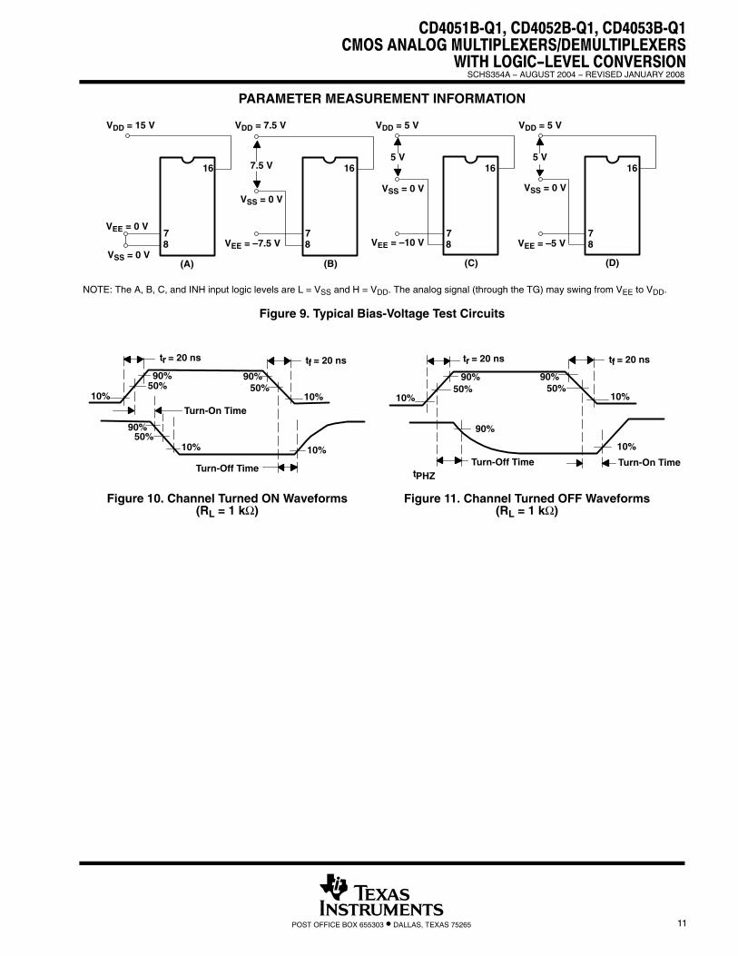
PARAMETER MEASUREMENT INFORMATION
NOTE: The A, B, C, and INH input logic levels are L = VSS and H = VDD. The analog signal (through the TG) may swing from VEE to VDD.
78
(B) (C) (D)(A)
1616 1616
78
78
78
5 V 5 V
VSS = 0 V
VSS = 0 VVSS = 0 VVSS = 0 V
VEE = –5 VVEE = –10 VVEE = –7.5 V
VEE = 0 V
VDD = 15 V VDD = 7.5 V VDD = 5 V VDD = 5 V
7.5 V
Figure 9. Typical Bias-Voltage Test Circuits
Figure 10. Channel Turned ON Waveforms(RL = 1 kΩ)
tf = 20 ns
10%
10%
90%50%
10%50%
90%
10%50%90%
tr = 20 ns
Turn-Off Time
Turn-On Time
Figure 11. Channel Turned OFF Waveforms(RL = 1 kΩ)
tf = 20 ns
10%
90%50%
10%50%
90%
10%
90%
tr = 20 ns
Turn-Off Time Turn-On TimetPHZ
CD4051B-Q1, CD4052B-Q1, CD4053B-Q1CMOS ANALOG MULTIPLEXERS/DEMULTIPLEXERSWITH LOGIC−LEVEL CONVERSIONSCHS354A − AUGUST 2004 − REVISED JANUARY 2008
12 POST OFFICE BOX 655303 • DALLAS, TEXAS 75265
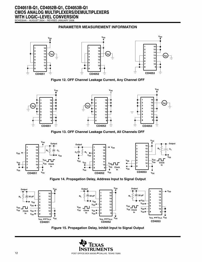
PARAMETER MEASUREMENT INFORMATION
1234567
8
16151413121110
9
CD4051
VDD
IDD
CD4052
12345678
16151413121110
9
CD4052
VDD
IDD
12345678
16151413121110
9
CD4053
VDD
IDD
Figure 12. OFF Channel Leakage Current, Any Channel OFF
12345678
16151413121110
9
CD4051
VDD
IDD
12345678
16151413121110
9
CD4052
VDD
IDD
12345678
16151413121110
9
CD4053
VDD
IDD
Figure 13. OFF Channel Leakage Current, All Channels OFF
VSS
RL
CD4051
ClockIn
Output
1234567
8
16151413121110
9
VDD
VDD
VEE
VSS
VDD
VSS
VEE
CL
VDD
CL
CD4052
ClockIn
Output12345678
16151413121110
9
VDD
VSS
VEE
VDD
VSS
VSS
VEE
RL
VDD
VDDVEE
VEE
VSS
VSS
VSS
CD4053
ClockIn
RL CL
Output12345678
161514131211109
Figure 14. Propagation Delay, Address Input to Signal Output
VSS
VEE
tPHL and tPLH
VSS
VDD
VSS
Output
CD4051
12345678
16151413121110
9Clock
In
50 pF
VDD
VEE
VDD
RL
VSS
VDD
VEEVSS
tPHL and tPLH
CD4052
12345678
16151413121110
9
Output
ClockIn
50 pFRL
VEE
VSS
VDD
VDD
VDD
VEE
VSS
VEE
tPHL and tPLH
ClockIn
CD4053
12345678
16151413121110
9
VDD
VDD
Output
RL
VSS
VSS
50 pF
Figure 15. Propagation Delay, Inhibit Input to Signal Output
CD4051B-Q1, CD4052B-Q1, CD4053B-Q1CMOS ANALOG MULTIPLEXERS/DEMULTIPLEXERS
WITH LOGIC−LEVEL CONVERSIONSCHS354A − AUGUST 2004 − REVISED JANUARY 2008
13POST OFFICE BOX 655303 • DALLAS, TEXAS 75265
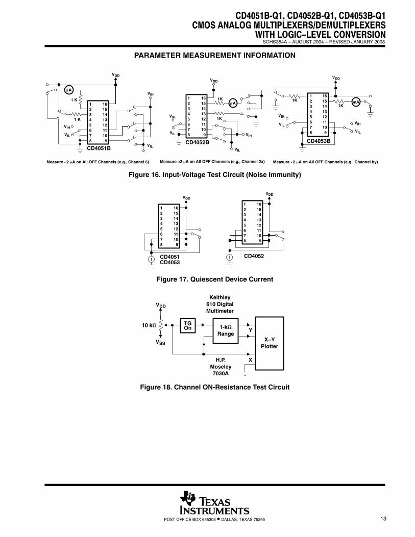
PARAMETER MEASUREMENT INFORMATION
VIL
CD4051B
µA
12345678 9
10111213141516
VIH
VIL
VIH
VDD
1 K
1 K
Measure 2 A on All OFF Channels (e.g., Channel 6)
VIL
VIH
1K
1K
µA
CD4052B
12345678 9
10111213141516
Measure 2 A on All OFF Channels (e.g., Channel 2x)
VDD
VIH
VIL
VIL
VIL
VIH
VIH
1K1K
VDD
CD4053B
12345678 9
10111213141516
Measure 2 A on All OFF Channels (e.g., Channel by)
mA
Figure 16. Input-Voltage Test Circuit (Noise Immunity)
CD4051CD4053
Ι
12345678 9
10111213141516
CD4052Ι
12345678 9
10111213141516
VDDVDD
Figure 17. Quiescent Device Current
X
YTGOn
Keithley610 DigitalMultimeter
H.P.Moseley7030A
X−YPlotter
1-kRange
VDD
VSS
10 k
Figure 18. Channel ON-Resistance Test Circuit
CD4051B-Q1, CD4052B-Q1, CD4053B-Q1CMOS ANALOG MULTIPLEXERS/DEMULTIPLEXERSWITH LOGIC−LEVEL CONVERSIONSCHS354A − AUGUST 2004 − REVISED JANUARY 2008
14 POST OFFICE BOX 655303 • DALLAS, TEXAS 75265
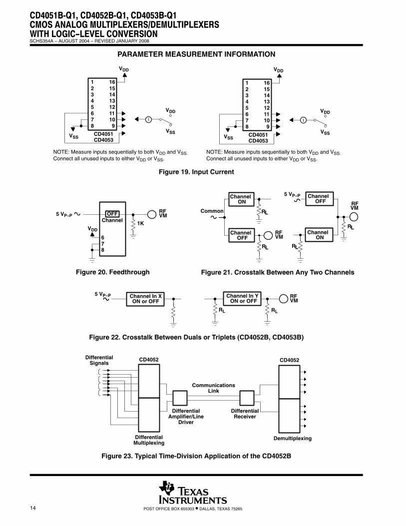
PARAMETER MEASUREMENT INFORMATION
NOTE: Measure inputs sequentially to both VDD and VSS. Connect all unused inputs to either VDD or VSS.
Ι
CD4053CD4051
12345678 9
10111213141516
VDD
VSS
VDD
VSS
NOTE: Measure inputs sequentially to both VDD and VSS. Connect all unused inputs to either VDD or VSS.
Ι
CD4053CD4051
12345678 9
10111213141516
VDD
VSS
VDD
VSS
Figure 19. Input Current
Figure 20. Feedthrough
RFVMOFF
Channel
678
1K
5 VP−P
VDD
Figure 21. Crosstalk Between Any Two Channels
RLCommon
ONChannel
RL
RFVM ON
ChannelRL
OFFChannel
RL
RFVM
OFFChannel
5 VP−P
5 VP−P RFVMON or OFF
Channel In Y
RLRL
ON or OFFChannel In X
Figure 22. Crosstalk Between Duals or Triplets (CD4052B, CD4053B)
.
Demultiplexing
CD4052 CD4052
DifferentialMultiplexing
CommunicationsLink
DifferentialReceiver
DifferentialAmplifier/Line
Driver
DifferentialSignals
Figure 23. Typical Time-Division Application of the CD4052B
CD4051B-Q1, CD4052B-Q1, CD4053B-Q1CMOS ANALOG MULTIPLEXERS/DEMULTIPLEXERS
WITH LOGIC−LEVEL CONVERSIONSCHS354A − AUGUST 2004 − REVISED JANUARY 2008
15POST OFFICE BOX 655303 • DALLAS, TEXAS 75265
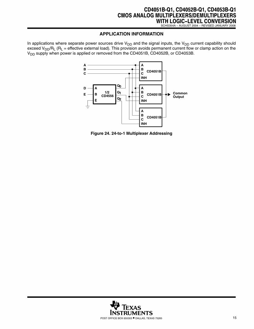
APPLICATION INFORMATION
In applications where separate power sources drive VDD and the signal inputs, the VDD current capability shouldexceed VDD/RL (RL = effective external load). This provision avoids permanent current flow or clamp action on theVDD supply when power is applied or removed from the CD4051B, CD4052B, or CD4053B.
A
B
E
1/2CD4556
ABC
CD4051B
INH
ABC CD4051B
INH
ABC
CD4051B
INH
ABC
D
E
Q0
Q1
Q2
CommonOutput
Figure 24. 24-to-1 Multiplexer Addressing
PACKAGE OPTION ADDENDUM
www.ti.com 28-Feb-2014
Addendum-Page 1
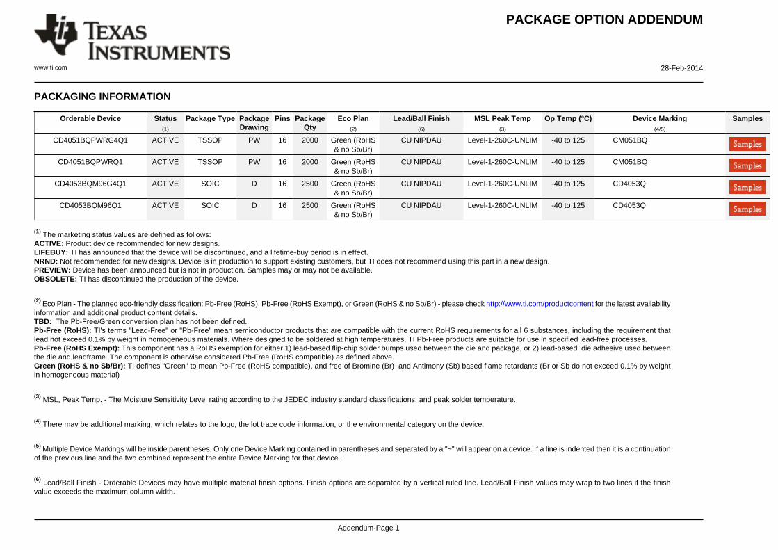
PACKAGING INFORMATION
Orderable Device Status(1)
Package Type PackageDrawing
Pins PackageQty
Eco Plan(2)
Lead/Ball Finish(6)
MSL Peak Temp(3)
Op Temp (°C) Device Marking(4/5)
Samples
CD4051BQPWRG4Q1 ACTIVE TSSOP PW 16 2000 Green (RoHS& no Sb/Br)
CU NIPDAU Level-1-260C-UNLIM -40 to 125 CM051BQ
CD4051BQPWRQ1 ACTIVE TSSOP PW 16 2000 Green (RoHS& no Sb/Br)
CU NIPDAU Level-1-260C-UNLIM -40 to 125 CM051BQ
CD4053BQM96G4Q1 ACTIVE SOIC D 16 2500 Green (RoHS& no Sb/Br)
CU NIPDAU Level-1-260C-UNLIM -40 to 125 CD4053Q
CD4053BQM96Q1 ACTIVE SOIC D 16 2500 Green (RoHS& no Sb/Br)
CU NIPDAU Level-1-260C-UNLIM -40 to 125 CD4053Q
(1) The marketing status values are defined as follows:ACTIVE: Product device recommended for new designs.LIFEBUY: TI has announced that the device will be discontinued, and a lifetime-buy period is in effect.NRND: Not recommended for new designs. Device is in production to support existing customers, but TI does not recommend using this part in a new design.PREVIEW: Device has been announced but is not in production. Samples may or may not be available.OBSOLETE: TI has discontinued the production of the device.
(2) Eco Plan - The planned eco-friendly classification: Pb-Free (RoHS), Pb-Free (RoHS Exempt), or Green (RoHS & no Sb/Br) - please check http://www.ti.com/productcontent for the latest availabilityinformation and additional product content details.TBD: The Pb-Free/Green conversion plan has not been defined.Pb-Free (RoHS): TI's terms "Lead-Free" or "Pb-Free" mean semiconductor products that are compatible with the current RoHS requirements for all 6 substances, including the requirement thatlead not exceed 0.1% by weight in homogeneous materials. Where designed to be soldered at high temperatures, TI Pb-Free products are suitable for use in specified lead-free processes.Pb-Free (RoHS Exempt): This component has a RoHS exemption for either 1) lead-based flip-chip solder bumps used between the die and package, or 2) lead-based die adhesive used betweenthe die and leadframe. The component is otherwise considered Pb-Free (RoHS compatible) as defined above.Green (RoHS & no Sb/Br): TI defines "Green" to mean Pb-Free (RoHS compatible), and free of Bromine (Br) and Antimony (Sb) based flame retardants (Br or Sb do not exceed 0.1% by weightin homogeneous material)
(3) MSL, Peak Temp. - The Moisture Sensitivity Level rating according to the JEDEC industry standard classifications, and peak solder temperature.
(4) There may be additional marking, which relates to the logo, the lot trace code information, or the environmental category on the device.
(5) Multiple Device Markings will be inside parentheses. Only one Device Marking contained in parentheses and separated by a "~" will appear on a device. If a line is indented then it is a continuationof the previous line and the two combined represent the entire Device Marking for that device.
(6) Lead/Ball Finish - Orderable Devices may have multiple material finish options. Finish options are separated by a vertical ruled line. Lead/Ball Finish values may wrap to two lines if the finishvalue exceeds the maximum column width.
PACKAGE OPTION ADDENDUM
www.ti.com 28-Feb-2014
Addendum-Page 2
Important Information and Disclaimer:The information provided on this page represents TI's knowledge and belief as of the date that it is provided. TI bases its knowledge and belief on informationprovided by third parties, and makes no representation or warranty as to the accuracy of such information. Efforts are underway to better integrate information from third parties. TI has taken andcontinues to take reasonable steps to provide representative and accurate information but may not have conducted destructive testing or chemical analysis on incoming materials and chemicals.TI and TI suppliers consider certain information to be proprietary, and thus CAS numbers and other limited information may not be available for release.
In no event shall TI's liability arising out of such information exceed the total purchase price of the TI part(s) at issue in this document sold by TI to Customer on an annual basis.
OTHER QUALIFIED VERSIONS OF CD4051B-Q1, CD4053B-Q1 :
• Catalog: CD4051B, CD4053B
• Military: CD4051B-MIL, CD4053B-MIL
NOTE: Qualified Version Definitions:
• Catalog - TI's standard catalog product
• Military - QML certified for Military and Defense Applications
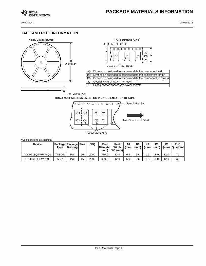
TAPE AND REEL INFORMATION
*All dimensions are nominal
Device PackageType
PackageDrawing
Pins SPQ ReelDiameter
(mm)
ReelWidth
W1 (mm)
A0(mm)
B0(mm)
K0(mm)
P1(mm)
W(mm)
Pin1Quadrant
CD4051BQPWRG4Q1 TSSOP PW 16 2000 330.0 12.4 6.9 5.6 1.6 8.0 12.0 Q1
CD4051BQPWRQ1 TSSOP PW 16 2000 330.0 12.4 6.9 5.6 1.6 8.0 12.0 Q1
PACKAGE MATERIALS INFORMATION
www.ti.com 14-Mar-2013
Pack Materials-Page 1
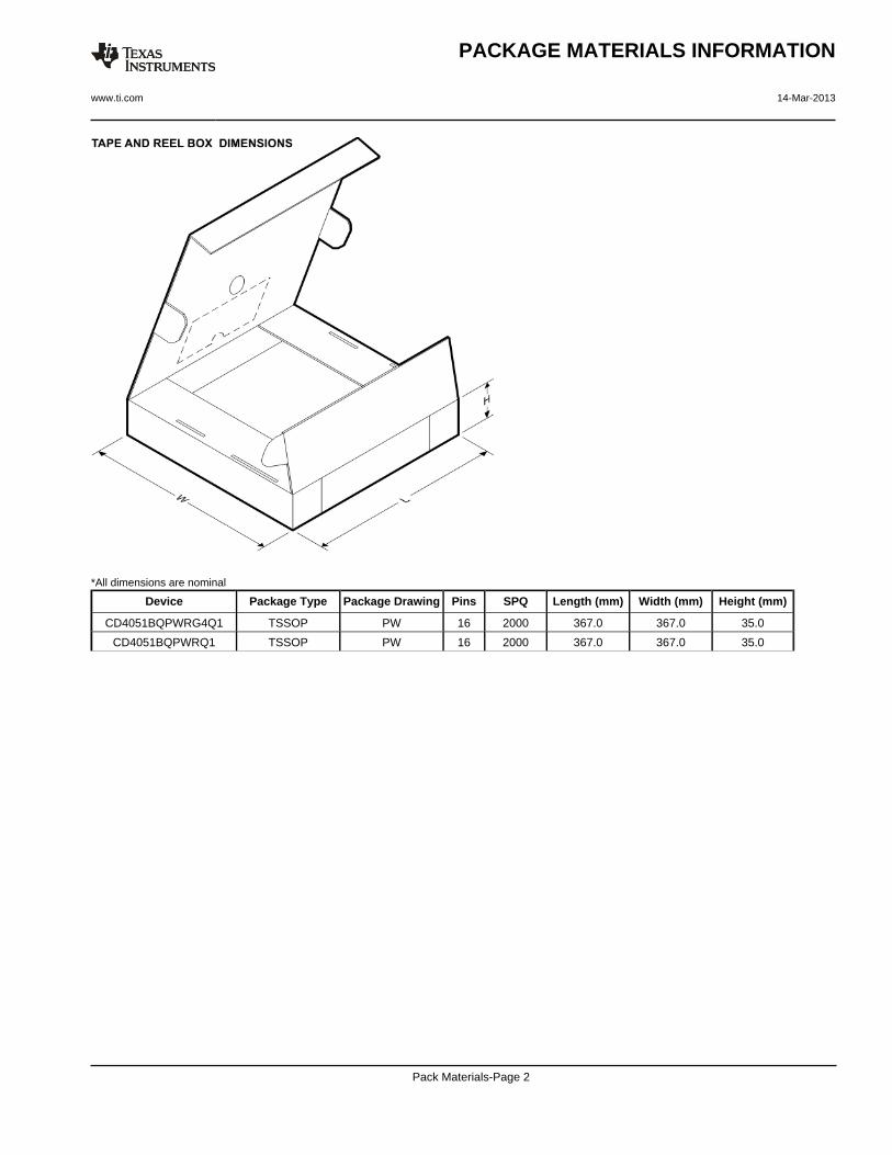
*All dimensions are nominal
Device Package Type Package Drawing Pins SPQ Length (mm) Width (mm) Height (mm)
CD4051BQPWRG4Q1 TSSOP PW 16 2000 367.0 367.0 35.0
CD4051BQPWRQ1 TSSOP PW 16 2000 367.0 367.0 35.0
PACKAGE MATERIALS INFORMATION
www.ti.com 14-Mar-2013
Pack Materials-Page 2
IMPORTANT NOTICE
Texas Instruments Incorporated and its subsidiaries (TI) reserve the right to make corrections, enhancements, improvements and otherchanges to its semiconductor products and services per JESD46, latest issue, and to discontinue any product or service per JESD48, latestissue. Buyers should obtain the latest relevant information before placing orders and should verify that such information is current andcomplete. All semiconductor products (also referred to herein as “components”) are sold subject to TI’s terms and conditions of salesupplied at the time of order acknowledgment.TI warrants performance of its components to the specifications applicable at the time of sale, in accordance with the warranty in TI’s termsand conditions of sale of semiconductor products. Testing and other quality control techniques are used to the extent TI deems necessaryto support this warranty. Except where mandated by applicable law, testing of all parameters of each component is not necessarilyperformed.TI assumes no liability for applications assistance or the design of Buyers’ products. Buyers are responsible for their products andapplications using TI components. To minimize the risks associated with Buyers’ products and applications, Buyers should provideadequate design and operating safeguards.TI does not warrant or represent that any license, either express or implied, is granted under any patent right, copyright, mask work right, orother intellectual property right relating to any combination, machine, or process in which TI components or services are used. Informationpublished by TI regarding third-party products or services does not constitute a license to use such products or services or a warranty orendorsement thereof. Use of such information may require a license from a third party under the patents or other intellectual property of thethird party, or a license from TI under the patents or other intellectual property of TI.Reproduction of significant portions of TI information in TI data books or data sheets is permissible only if reproduction is without alterationand is accompanied by all associated warranties, conditions, limitations, and notices. TI is not responsible or liable for such altereddocumentation. Information of third parties may be subject to additional restrictions.Resale of TI components or services with statements different from or beyond the parameters stated by TI for that component or servicevoids all express and any implied warranties for the associated TI component or service and is an unfair and deceptive business practice.TI is not responsible or liable for any such statements.Buyer acknowledges and agrees that it is solely responsible for compliance with all legal, regulatory and safety-related requirementsconcerning its products, and any use of TI components in its applications, notwithstanding any applications-related information or supportthat may be provided by TI. Buyer represents and agrees that it has all the necessary expertise to create and implement safeguards whichanticipate dangerous consequences of failures, monitor failures and their consequences, lessen the likelihood of failures that might causeharm and take appropriate remedial actions. Buyer will fully indemnify TI and its representatives against any damages arising out of the useof any TI components in safety-critical applications.In some cases, TI components may be promoted specifically to facilitate safety-related applications. With such components, TI’s goal is tohelp enable customers to design and create their own end-product solutions that meet applicable functional safety standards andrequirements. Nonetheless, such components are subject to these terms.No TI components are authorized for use in FDA Class III (or similar life-critical medical equipment) unless authorized officers of the partieshave executed a special agreement specifically governing such use.Only those TI components which TI has specifically designated as military grade or “enhanced plastic” are designed and intended for use inmilitary/aerospace applications or environments. Buyer acknowledges and agrees that any military or aerospace use of TI componentswhich have not been so designated is solely at the Buyer's risk, and that Buyer is solely responsible for compliance with all legal andregulatory requirements in connection with such use.TI has specifically designated certain components as meeting ISO/TS16949 requirements, mainly for automotive use. In any case of use ofnon-designated products, TI will not be responsible for any failure to meet ISO/TS16949.
Products ApplicationsAudio www.ti.com/audio Automotive and Transportation www.ti.com/automotiveAmplifiers amplifier.ti.com Communications and Telecom www.ti.com/communicationsData Converters dataconverter.ti.com Computers and Peripherals www.ti.com/computersDLP® Products www.dlp.com Consumer Electronics www.ti.com/consumer-appsDSP dsp.ti.com Energy and Lighting www.ti.com/energyClocks and Timers www.ti.com/clocks Industrial www.ti.com/industrialInterface interface.ti.com Medical www.ti.com/medicalLogic logic.ti.com Security www.ti.com/securityPower Mgmt power.ti.com Space, Avionics and Defense www.ti.com/space-avionics-defenseMicrocontrollers microcontroller.ti.com Video and Imaging www.ti.com/videoRFID www.ti-rfid.comOMAP Applications Processors www.ti.com/omap TI E2E Community e2e.ti.comWireless Connectivity www.ti.com/wirelessconnectivity
Mailing Address: Texas Instruments, Post Office Box 655303, Dallas, Texas 75265Copyright © 2016, Texas Instruments Incorporated