C . , I N C T O R D U MPC821 O N Applications Development...
198
Motorola Semiconductor Israel Ltd. MOTOROLA MOTOROLA COMMUNICATIONS & ADVANCED CONSUMER TECHNOLOGY GROUP SIX SIGMA 6 σ MPC821 ISSUE 1.4b - Rev B Release, 8/15/97 Applications Development System (ADS) Users Manual Revision B ARCHIVED BY FREESCALE SEMICONDUCTOR, INC.
Transcript of C . , I N C T O R D U MPC821 O N Applications Development...
Motorola Semiconductor Israel Ltd.
MOTOROLA
MOTOROLA
COMMUNICATIONS & ADVANCED
CONSUMER TECHNOLOGY GROUP
SIX SIGMA
6
σ
MPC821
ISSUE 1.4b - Rev B Release, 8/15/97
Applications DevelopmentSystem (ADS)UserÕs Manual
Revision BARCHIVED BY FREESCALE SEMICONDUCTOR, IN
C.
MPC821ADS User’s Manual (Revision B)
i
Release 1.4b
Table of Contents
Section 1General Information ........................................................................................................... ...... 1
Introduction ..................................................................................................................... 1Abbreviation List .............................................................................................................. 1Related Documentation ................................................................................................... 1Specifications .................................................................................................................. 2MPC821ADS Features .................................................................................................... 3Revision A to Revision B Changes ................................................................................. 5Revision Pilot to Revision A Changes ............................................................................. 5Revision ENG to Revision Pilot Changes ....................................................................... 5
Section 2Hardware Preparation and Installation .................................................................................. 8
Introduction ..................................................................................................................... 8Unpacking Instructions .................................................................................................... 8Hardware Preparation ..................................................................................................... 8
ADI Port Address Selection ................................................................................ 10Clock Source Selection ...................................................................................... 10Power-On Reset Source Selection ..................................................................... 12VDDL Source Selection ...................................................................................... 12Keep Alive Power Source Selection ................................................................... 13
Installation Instructions .................................................................................................. 13Host Controlled Operation .................................................................................. 14Debug Port Controller For Target System .......................................................... 14Stand Alone Operation ....................................................................................... 16+5V Power Supply Connection .......................................................................... 16P8: +12V Power Supply Connection .................................................................. 17ADI Installation ................................................................................................... 17Host computer to MPC821ADS Connection ...................................................... 17Terminal to MPC821ADS RS-232 Connection ................................................... 18Memory Installation ............................................................................................ 18
Section 3Operating Instructions ......................................................................................................... .. 20
Introduction ................................................................................................................... 20Controls and Indicators ................................................................................................. 20
SOFT RESET Switch SW1 ................................................................................ 20ABORT Switch SW2 ........................................................................................... 20HARD RESET - Switches SW1 & SW2 .............................................................. 20DS2 - Software Options Switch .......................................................................... 20J4 Power Bridge ................................................................................................. 21GND Bridges ...................................................................................................... 21RUN Indicator - LD1 ........................................................................................... 21FLASH ON - LD2 ................................................................................................ 21
ARCHIVED BY FREESCALE SEMICONDUCTOR, INC.
MPC821ADS User’s Manual (Revision B)
ii
Release 1.4b
DRAM ON - LD3 ................................................................................................. 21ETH ON - LD4 .................................................................................................... 21Ethernet RX Indicator - LD5 ............................................................................... 21Ethernet TX Indicator - LD6 ................................................................................ 21Ethernet JABB Indicator - LD7 ........................................................................... 21IRD ON - LD8 ..................................................................................................... 22Ethernet CLSN Indicator LD9 ............................................................................. 22Ethernet PLR Indicator - LD10 ........................................................................... 22Ethernet LIL Indicator - LD11 ............................................................................. 22RS232 Port 1 ON - LD12 .................................................................................... 22PCMCIA ON - LD13 ........................................................................................... 22RS232 Port 2 ON - LD14 .................................................................................... 225V Indicator - LD15 ............................................................................................ 223.3V Indicator - LD16 ......................................................................................... 22
Memory Map ................................................................................................................. 23Programming The MPC821 Registers .......................................................................... 24
Memory Controller Registers Programming ....................................................... 24
Section 4Functional Description ........................................................................................................ .. 37
MPC821 ........................................................................................................................ 37Reset & Reset - Configuration ...................................................................................... 37
Keep Alive Power-On Reset ............................................................................... 37Main Power - On Reset ...................................................................................... 37Manual Soft Reset .............................................................................................. 38Manual Hard Reset ............................................................................................ 38MPC821 Internal Sources .................................................................................. 38Reset Configuration ............................................................................................ 38
Local Interrupter ............................................................................................................ 39Clock Generator ............................................................................................................ 40
SPLL Support ..................................................................................................... 40Buffering ........................................................................................................................ 40Chip-Select Generator .................................................................................................. 40DRAM ............................................................................................................................ 41
DRAM 16 Bit Operation ...................................................................................... 42DRAM Performance Figures .............................................................................. 42Refresh Control .................................................................................................. 43Variable Bus-Width Control ................................................................................ 44
Flash Memory ............................................................................................................... 46Ethernet Port ................................................................................................................. 47Infra - Red Port .............................................................................................................. 47RS232 Ports .................................................................................................................. 48
RS-232 Port 1 or 2 Signal Description ............................................................... 48PCMCIA Port ................................................................................................................. 48
PCMCIA Power Control ...................................................................................... 49LCD Port ....................................................................................................................... 49
ARCHIVED BY FREESCALE SEMICONDUCTOR, INC.
MPC821ADS User’s Manual (Revision B)
iii
Release 1.4b
Board Control & Status Register - BCSR ...................................................................... 51BCSR Disable Protection Logic .......................................................................... 51BCSR0 - Hard Reset Configuration Register ..................................................... 52BCSR1 - Board Control Register ........................................................................ 53BCSR2 - Board Status Register - 1 .................................................................... 55BCSR3 - Auxiliary Control / Status Register ...................................................... 58
Debug Port Controller ................................................................................................... 59MPC821ADS As Debug Port Controller For Target System .............................. 60Debug Port Control / Status Register ................................................................. 62Standard MPCXXX Debug Port Connector Pin Description ............................... 63
Power ............................................................................................................................ 645V Bus ................................................................................................................ 663.3V Bus ............................................................................................................. 662V Bus ................................................................................................................ 6612V Bus .............................................................................................................. 66Keep Alive Power ............................................................................................... 66
Section 5Support Information ........................................................................................................... ... 67
Interconnect Signals ...................................................................................................... 67P1 ADI - Port Connector ..................................................................................... 68P2 - Ethernet Port Connector ............................................................................. 69P3 - RS232 Ports’ Connectors ........................................................................... 69PCMCIA Port Connector .................................................................................... 70P5 - External Debug Port Controller Input Interconnect. ..................................... 73P6, P9, P10 & P12 Expansion and Logic Analyzer Connectors ........................ 74P7 - 5V Power Connector ................................................................................... 95P8 - 12V Power Connector ................................................................................. 95P11 - LCD Connector ......................................................................................... 95P13 - QUADS Compatible Communication Connector ...................................... 96
MPC821ADS Part List ................................................................................................. 101
Appendix AProgrammable Logic Equations ......................................................................................... 107
U7 - Debug Port Controller .......................................................................................... 108U10 - Auxiliary Board Control ...................................................................................... 134U11 - Board Control & Status Register ....................................................................... 151
Appendix BADI I/F .................................................................................................................................... 183
ADI Port Signal Description ......................................................................................... 184
ARCHIVED BY FREESCALE SEMICONDUCTOR, INC.
MPC821ADS User’s Manual (Revision B)
iv
Release 1.4b
Appendix CADI Installation .............................................................................................................. ....... 185
Introduction ................................................................................................................. 185IBM-PC/XT/AT to MPC821ADS Interface ................................................................... 185
ADI Installation in IBM-PC/XT/AT ..................................................................... 185SUN-4 to MPC821ADS Interface ................................................................................ 188
ADI Installation in the SUN-4 ............................................................................ 188Revision B Schematics ................................................................................................ 190
Figures
Figure 1-1 MPC821ADS Block Diagram .................................................................................... 4Figure 2-1 MPC821ADS Top Side Part Location diagram ........................................................ 9Figure 2-2 Configuration Dip-Switch - DS1 ............................................................................. 10Figure 2-3 U17 Power Sources ................................................................................................ 11Figure 2-4 Power-On Reset Source Selection ......................................................................... 12Figure 2-5 VDDL Source Selection .......................................................................................... 12Figure 2-6 Keep Alive Power Source Selection ....................................................................... 13Figure 2-7 Host Controlled Operation Scheme ........................................................................ 14Figure 2-8 Debug Port Controller For Target System Operation Scheme ............................... 15Figure 2-9 Stand Alone Configuration ...................................................................................... 16Figure 2-10 P7: +5V Power Connector .................................................................................... 16Figure 2-11 P8: +12V Power Connector .................................................................................. 17Figure 2-12 P1 - ADI Port Connector ....................................................................................... 17Figure 2-13 P3 - RS-232 Serial Port Connector ...................................................................... 18Figure 2-14 Memory SIMM Installation .................................................................................... 19
Figure 3-1 DS2 - Description ................................................................................................... 20
Figure 4-1 Refresh Scheme...................................................................................................... 43Figure 4-2 DRAM Address Lines’ Switching ............................................................................ 45Figure 4-3 Flash Memory SIMM Architecture .......................................................................... 46Figure 4-4 RS-232 Serial Port 1 or 2 Connector ...................................................................... 48Figure 4-5 PCMCIA Port Configuration .................................................................................... 50Figure 4-6 Debug Port Controller Block Diagram .................................................................... 60Figure 4-7 Standard Debug Port Connector ............................................................................ 63Figure 4-8 MPC821ADS Power Scheme ................................................................................. 65
Figure 5-1 Expansion Connector Assembly.............................................................................. 75
ARCHIVED BY FREESCALE SEMICONDUCTOR, INC.
MPC821ADS User’s Manual (Revision B)
v
Release 1.4b
Figure B-1 ADI Port Connector .............................................................................................. 183
Figure C-1 Physical Location of jumper JG1 and JG2 on Original ADI ................................. 186Figure C-2 JG1 Configuration Options ................................................................................... 186Figure C-3 Physical Location of jumper JG1 and JG2 ........................................................... 187Figure C-4 JG2 Configuration Options ................................................................................... 188Figure C-5 ADI board for SBus .............................................................................................. 189
Tables
Table 1-1 MPC821ADS Specifications ...................................................................................... 2
Table 2-1 ADI Address Selection ............................................................................................. 10
Table 3-1 MPC821ADS Main Memory Map.............................................................................. 23Table 3-2 SIU Register Programming ...................................................................................... 24Table 3-3 Memory Controller Initializations For 50Mhz ........................................................... 25Table 3-4 UPMA Initializations for 60nsec DRAMs @ 50MHz ................................................ 27Table 3-5 UPMA Initializations for 70nsec DRAMs @ 50MHz ................................................ 28Table 3-6 UPMA Initializations for 60nsec EDO DRAMs @ 50MHz ........................................ 29Table 3-7 UPMA Initializations for 70nsec EDO DRAMs @ 50MHz ........................................ 30Table 3-8 Memory Controller Initializations For 25Mhz ........................................................... 30Table 3-9 UPMA Initializations for 60nsec DRAMs @ 25MHz ................................................ 33Table 3-10 UPMA Initializations for 70nsec DRAMs @ 25MHz .............................................. 34Table 3-11 UPMA Initializations for 60nsec EDO DRAMs @ 25MHz ...................................... 35Table 3-12 UPMA Initializations for 70nsec EDO DRAMs @ 25MHz ...................................... 36
Table 4-1 Regular DRAM Performance Figures ....................................................................... 42Table 4-2 EDO DRAM Performance Figures ........................................................................... 43Table 4-3 DRAM Address Connections ................................................................................... 45Table 4-4 Flash Memory Performance Figures ....................................................................... 47Table 4-5 BCSR0 Description .................................................................................................. 52Table 4-6 BCSR1 Description .................................................................................................. 53Table 4-7 PCCVPP(0:1) Assignment ....................................................................................... 54Table 4-8 BCSR2 Description .................................................................................................. 55Table 4-9 Flash Presence Detect (4:1) Encoding .................................................................... 56Table 4-10 DRAM Presence Detect (2:1) Encoding ................................................................ 56Table 4-11 DRAM Presence Detect (4:3) Encoding ................................................................ 56Table 4-12 EXTOOLI(0:3) Assignment .................................................................................... 57Table 4-13 BCSR3 Description ................................................................................................ 58Table 4-14 MPC821ADS Revision Number Conversion Table ................................................ 59Table 4-15 FLASH Presence Detect (7:5) Encoding ............................................................... 59Table 4-16 Debug Port Control / Status Register .................................................................... 62Table 4-17 DSCK Frequency Select ........................................................................................ 63Table 4-18 Off-board Application Maximum Current Consumption ......................................... 65
ARCHIVED BY FREESCALE SEMICONDUCTOR, INC.
MPC821ADS User’s Manual (Revision B)
vi
Release 1.4b
Table 5-1 P1 - ADI Port Interconnect Signals ........................................................................... 68Table 5-2 P2 - Ethernet Port Interconnect Signals .................................................................. 69Table 5-3 PA3 or PB3 - Interconnect Signals .......................................................................... 69Table 5-4 P4 - PCMCIA Connector Interconnect Signals ........................................................ 70Table 5-5 P5 - Interconnect Signals ......................................................................................... 73Table 5-6 P6 - Interconnect Signals ......................................................................................... 75Table 5-7 P9 - Interconnect Signals ......................................................................................... 80Table 5-8 P10 - Interconnect Signals ....................................................................................... 86Table 5-9 P12 - Interconnect Signals ....................................................................................... 91Table 5-10 P7 - Interconnect Signals ....................................................................................... 95Table 5-11 P8 - Interconnect Signals ....................................................................................... 95Table 5-12 P11 - Interconnect Signals ..................................................................................... 95Table 5-13 P13 - Interconnect Signals ..................................................................................... 96Table 5-14 MPC821ADS Part List ......................................................................................... 101
ARCHIVED BY FREESCALE SEMICONDUCTOR, INC.

MPC821ADS User’s Manual (Revision B)
1
Release 1.4b
General Information
1 - General Information
1•1 Introduction
This document is an operation guide for the MPC821ADS board. It contains operational, functional andgeneral information about the ADS. The MPC821ADS is meant to serve as a platform for s/w and h/w de-velopment around the MPC821. Using its on-board resources and its associated debugger, a developer isable to load his code, run it, set breakpoints, display memory and registers and connect his own proprietaryh/w via the expansion connectors, to be incorporated to a desired system with the pda.
This board could also be used as a demonstration tool, i.e., application s/w may be burned
A
into its flashmemory and ran in exhibitions etc‘.
1•2 Abbreviation List
• PDA - Personal Digital Assistant, the MPC821
• UPM - User Programmable Machine
• GPCM - General Purpose Chip-select Machine
• GPL - General Purpose Line (associated with the UPM)
• I/R - Infra-Red
• MPC821ADS - the MPC821ADS, the subject of this document.
• BSCR - Board Control & Status Register.
• ZIF - Zero Input Force
• BGA - Ball Grid Array
1•3 Related Documentation
• MPC821 User’s Manual.
• MC68160 Data Sheet.
• ADI Board Specification.
A. Either on or off-board.
ARCHIVED BY FREESCALE SEMICONDUCTOR, INC.
MPC821ADS User’s Manual (Revision B)
2
Release 1.4b
General Information
1•4 Specifications
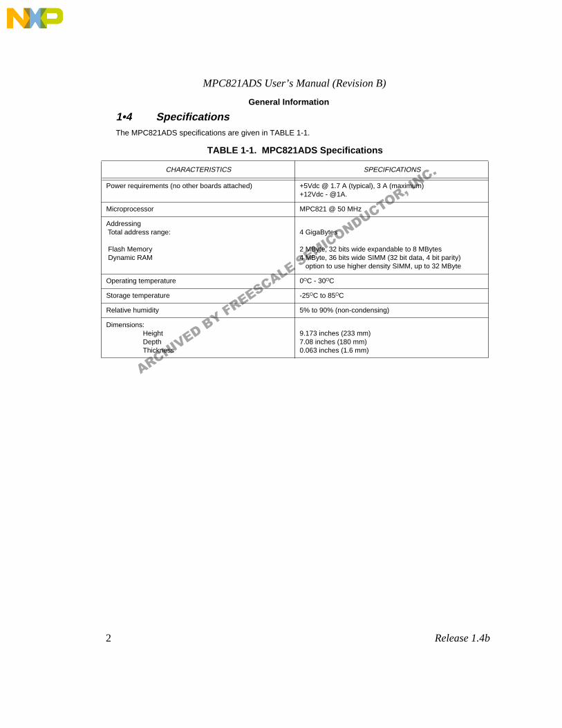
The MPC821ADS specifications are given in TABLE 1-1.
TABLE 1-1. MPC821ADS Specifications
CHARACTERISTICS SPECIFICATIONS
Power requirements (no other boards attached) +5Vdc @ 1.7 A (typical), 3 A (maximum)+12Vdc - @1A.
Microprocessor MPC821 @ 50 MHz
Addressing Total address range: Flash Memory Dynamic RAM
4 GigaBytes
2 MByte, 32 bits wide expandable to 8 MBytes4 MByte, 36 bits wide SIMM (32 bit data, 4 bit parity) option to use higher density SIMM, up to 32 MByte
Operating temperature 0
O
C - 30
O
C
Storage temperature -25
O
C to 85
O
C
Relative humidity 5% to 90% (non-condensing)
Dimensions: Height Depth Thickness
9.173 inches (233 mm)7.08 inches (180 mm)0.063 inches (1.6 mm)
ARCHIVED BY FREESCALE SEMICONDUCTOR, INC.

MPC821ADS User’s Manual (Revision B)
3
Release 1.4b
General Information
1•5 MPC821ADS Features
MPC821, running up to 50 MHz, mounted on ZIF BGA socket.
4 MBytes of 60-nsec EDO DRAM, support is given to various types of DRAM varying from4MByte configured as 1M X 32, upto 32MByte configured as 8M X 32.
Automatic Dram SIMM identification.
2 MByte Flash SIMM. Support for upto 8 MByte.
Automatic Flash SIMM identification.
Memory Disable Option for all local memory map slaves.
Board Control & Status Register - BCSR, Controlling Board’s Operation.
Programmable Hard-Reset Configuration via BCSR.
T.P. Ethernet port via MC68160 - EEST on SCC1 with Standby Mode.
Infra-Red Transceiver on SCC2 with Shutdown Option.
5V-only PCMCIA Socket With Full Buffering, Power Control and Port Disable Option. Com-plies with PCMCIA 2.1+ Standard.
Module Enable Indications.
RS232 port on SMC1 with Low-Power Option.
RS232 port on SMC2 with Low-Power Option.
On - Board Debug Port Controller with ADI I/F.
MPC821ADS Serving as Debug Station for Target System option.
Debug Clock Frequency Control - support for 10 / 5 / 2.5 / 1.25 MHz debug clock, SW pro-grammable.
LCD Display Connector.
Optional Hard-Reset Configuration Burned in Flash
A
.
All MPC821 Pins Available At Expansion & Logic Analyzer Connectors.
External Tools’ Identification Capability, via BCSR.
Soft / Hard Reset Push - Button
ABORT Push - Button
Single
B
5V Supply.
Reverse / Over Voltage Protection for Power Inputs.
A. Available only if supported also on-chip.B. Unless a 12V supply is required for a PCMCIA card.
ARCHIVED BY FREESCALE SEMICONDUCTOR, INC.
MPC821ADS User’s Manual (Revision B)
4
Release 1.4b
General Information
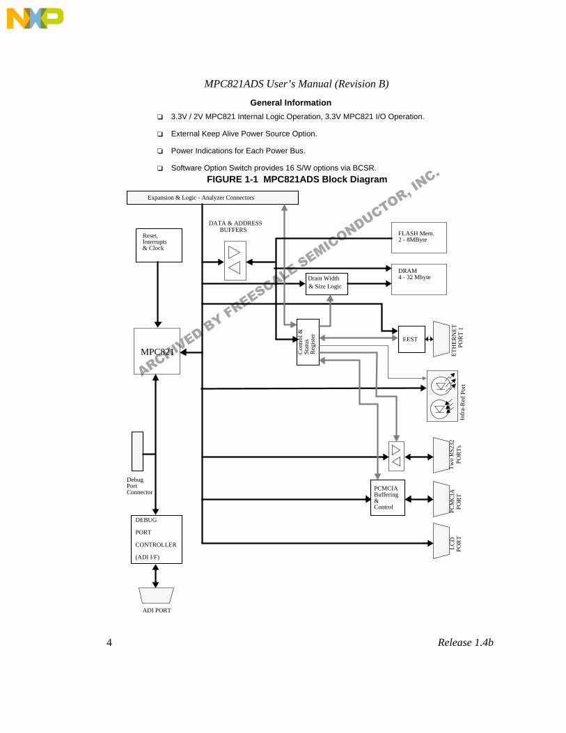
3.3V / 2V MPC821 Internal Logic Operation, 3.3V MPC821 I/O Operation.
External Keep Alive Power Source Option.
Power Indications for Each Power Bus.
Software Option Switch provides 16 S/W options via BCSR.
FIGURE 1-1 MPC821ADS Block Diagram
FLASH Mem.2 - 8MByte
DRAM4 - 32 Mbyte
EEST
DATA & ADDRESSBUFFERS
ET
HE
RN
ET
P
OR
T 1
Infr
a-R
ed P
ort
Tw
o R
S23
2 P
OR
Ts
PC
MC
IA
PO
RT
DEBUG
PORT
CONTROLLER
(ADI I/F)
Expansion & Logic - Analyzer Connectors
LCD
P
OR
T
MPC821
Reset,Interrupts& Clock
Con
trol
&
Sta
tus
Reg
iste
r
Dram Width& Size Logic
PCMCIABuffering&Control
DebugPortConnector
ADI PORT
ARCHIVED BY FREESCALE SEMICONDUCTOR, INC.

MPC821ADS User’s Manual (Revision B)
5
Release 1.4b
General Information
1•6 Revision A to Revision B Changes
1) Added restraining resistors over Dram SIMM address lines and Flash SIMM strobe lines. Exist-ing restraining resistors, over dram strobe lines, which were glued-in with revision A, are intro-duced into the PCB.
2) Fixed support for SM732A1000A and SM732A2000 by Smart.
3) Added 2’nd RS232 port over SMC2, with its own dedicated Enable bit in BCSR1.
4) RS232 connector is replaced with a stacked connector block, to support both RS232 ports.
5) Added 4 pull-up resistors over the MSB of each Byte of Dram data lines. This allows for normal FPM / EDO discrimination.
6) Additional support for external tools: DS1/4 state replaces GND in P9(D20), BRS_EN2~ replac-es GND in P12(B22) and N.C. in P13(C6). Since ready made tools for previous revisions might have connected these signals to GND, both are protected with series resistors.
7) Revision field in BCSR3 was changed to’0011’.
1•7 Revision Pilot to Revision A Changes
1) DS2 which on PILOT revision was connected on SP2 with blue wires, is now integrated into the PCB, located nearby SP2.
2) UA38 which on revision PILOT was glued and connected with blue-wires, is now integrated into the PCB. Gate allocation within UA38, is different from revision PILOT, to provide better PCB routing.
3) Revision code in BCSR is changed to 2.
4) Added optional RA21 (0 ohm) and CA7 (0.01
µ
F) for 10-Base-T interface network.
5) Some SMD pads were enlarged to assist manufacturing.
1•8 Revision ENG to Revision PILOT Changes
1) Added support for ads to function as debug station:
• Added independent 20MHz clock generator for debug port controller
• Added MUX (U38) so that internal logic is clocked by the above generator
• Removed pervious debug clock logic, derived from CLKOUT of the MPC821.
• Added signal named CHINS~ (CHip-In-Socket, active-low) which is connected to oneof the MPC821's GND pins (isolated from GND layer). This signal controls the abovemux and the indication LEDs illumination.
• Added pull-up resistors on the Chip-Select lines, to avoid possible data-bus contentionwhen MPC821 is off-socket.
• DRAMEN~ becomes active-low to allow buffer manipulation supporting LEDs dark-ness when MPC821 off-socket. Signal RUN becomes active-high from the same rea-son.
(Sh. 1, 7, 8, 9, 11, 14)
2) Signals EXTM(1:4) changed to BADDR(28:30),AS~ correspondingly, to support future external master support. (Sh. 1, 11, 13)
3) MODCK0 renamed to MODCK2, to comply with MPC821’s spec convention. (Sh 1, 3, 13)
4) Signal BCLOS~, which was optional for data buffers’ enable logic, is found redundant and re-moved from ADS logic. Renamed to GPL4A~. (Sh 1, 2, 3, 12)
ARCHIVED BY FREESCALE SEMICONDUCTOR, INC.

MPC821ADS User’s Manual (Revision B)
6
Release 1.4b
General Information
5) Added 3 Flash memory Presence Detect lines - F_PD(5:7) to BCSR (U11/65:67) (ENG - U10) to support varying flash memory delays. (Sh 3, 4, 11)
6) Added support for SMART flash simms:
• 12V VPP connected to SIMM
• BA10 connected also to the SIMM, to support 1M X 8 devices
(Sh. 4)
7) BCSR power on reset logic was changed to support board’s power-up recovery when keep-alive power remained active. (Sh. 3, 9)
8) Power-on reset logic changes:
• KA power-on reset is not driven by U10 (ENG - U9) but directly to the MPC821.
• Added AC14 (U23) powered by KAPWR to support this. (AC14’s s-t is required formach connection due to slow rise time of PORST~)
• D3 and R12 powered from KAPWR from the same reason.
• Added option for PON reset by main 3.3V bus. (J1)
(Sh. 3, 9)
9) BA9 and BA10 are connected to U10 (ENG - U9) instead of BA11 and BA12, for flash bank se-lection. Bug correction. (Sh. 3)
10) Renewed support for 32Khz crystal:
• CLK4IN is gated (UA38), so when working with 32768 Hz crystal, CLK4IN is drivenconstantly to '0'. This, to avoid clock jitter with this mode of operation.
• Parallel resistor increased to 20M
Ω
.
(Sh. 7)
11) PLL’s XFC capacitors were changed to react for formula change. Lower MF range capacitor is changed to 5nF to cover 1:5 to 1:10 MF range, while higher MF range capacitor was changed to 0.68uF to cover 1:458
A
to 1:1220
B
MF range
(Sh. 7)
12) PCMCIA power controller is changed to LTC1315 (by Linear Technologies):
• PCCVPPG~ signal and indication are removed, not supported by this device
• VPP selection code is changed.
• DRAMEN no longer controls power to the dram.
• Old 12V voltage pump remains as contingency for possible unavailability of the device,although the device switching outputs drive 12V. R55, R56 & R59 are therefore not as-sembled.
(Sh. 3, 9)
A. Lowest MF allowed with 32768 Hz crystal, due to 15MHz minimal PLL frequency.B. Highest MF allowed with 32768 Hz crystal, considering 40MHz rated MPC821.
ARCHIVED BY FREESCALE SEMICONDUCTOR, INC.

MPC821ADS User’s Manual (Revision B)
7
Release 1.4b
General Information
13) Added ADS board revision tag in BCSR.
14) Added signals RS_EN~ and ETHEN~ to P13 - Quads Compatible connector, for tool designer benefit. (Sh. 16)
15) Added 4-switches dip-switch - DS2, connected over EXTOLI(0:3) lines, to provide s/w option se-lection capability.
ARCHIVED BY FREESCALE SEMICONDUCTOR, INC.
MPC821ADS User’s Manual (Revision B)
8
Release 1.4b
Hardware Preparation and Installation
2 - Hardware Preparation and Installation
2•1 INTRODUCTION
This chapter provides unpacking instructions, hardware preparation, and installation instructions for theMPC821ADS.
2•2 UNPACKING INSTRUCTIONS
NOTE
If the shipping carton is damaged upon receipt, request carrier’s agent to be present during unpacking and in-spection of equipment.
Unpack equipment from shipping carton. Refer to packing list and verify that all items are present. Savepacking material for storing and reshipping of equipment.
CAUTION
AVOID TOUCHING AREAS OF INTEGRATED CIRCUIT-RY; STATIC DISCHARGE CAN DAMAGE CIRCUITS.
2•3 HARDWARE PREPARATION
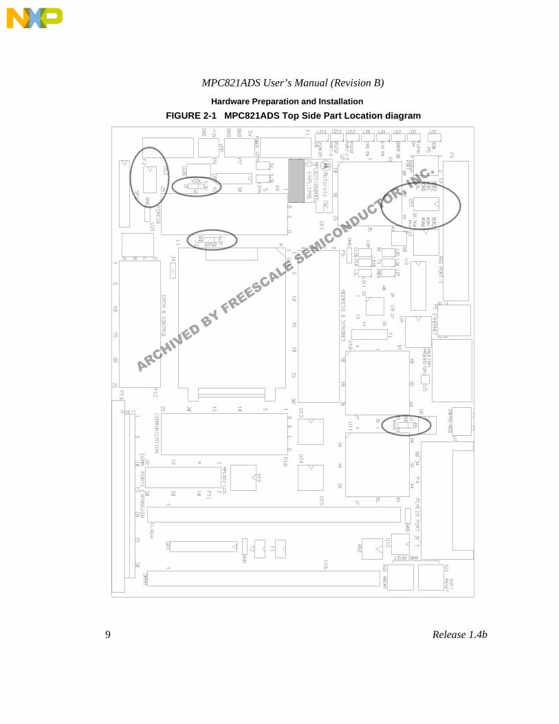
To select the desired configuration and ensure proper operation of the MPC821ADS board, changes of theDip-Switch settings may be required before installation. The location of the switches, LEDs, Dip-Switches,and connectors is illustrated in FIGURE 2-1. The board has been factory tested and is shipped with Dip-Switch settings as described in the following paragraphs. Parameters can be changed for the followingconditions:
• ADI port address
• MPC821 Clock Source
• Power-On Reset Source.
• MPC821 Keep Alive Power Source
• MPC821 Internal Logic Supply Source
ARCHIVED BY FREESCALE SEMICONDUCTOR, INC.
MPC821ADS User’s Manual (Revision B)
9
Release 1.4b
Hardware Preparation and Installation
FIGURE 2-1 MPC821ADS Top Side Part Location diagram
ARCHIVED BY FREESCALE SEMICONDUCTOR, INC.
MPC821ADS User’s Manual (Revision B)
10
Release 1.4b
Hardware Preparation and Installation
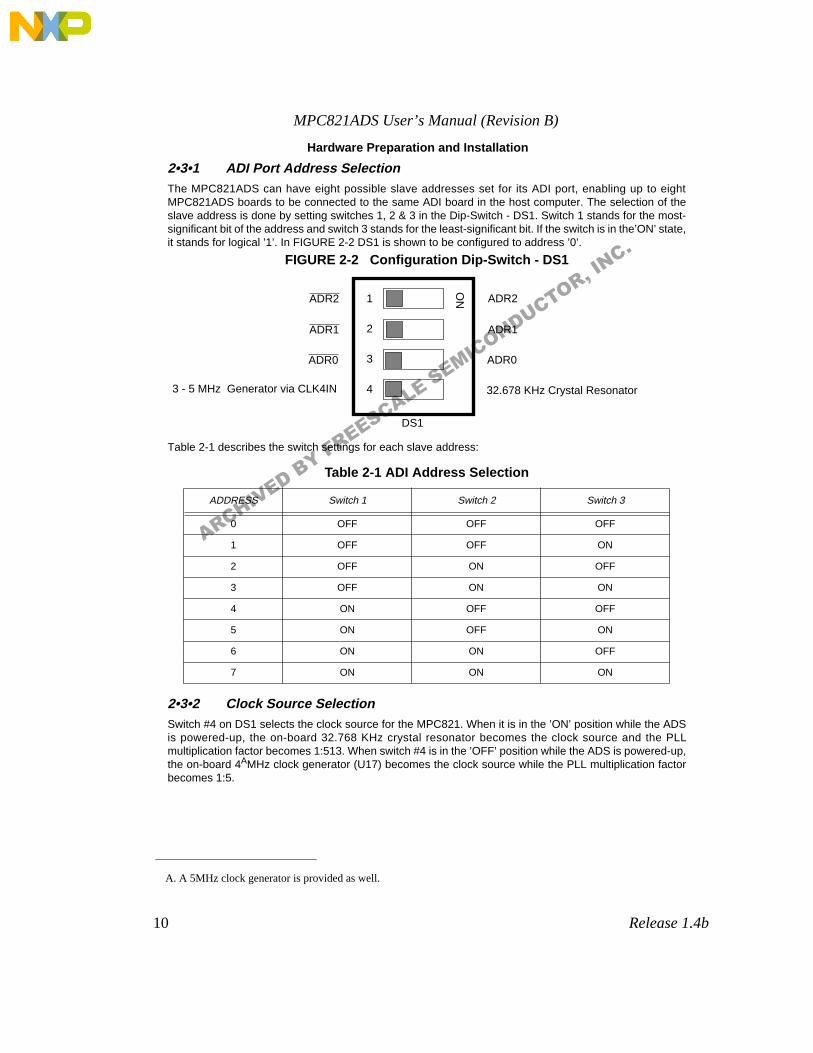
2•3•1 ADI Port Address Selection
The MPC821ADS can have eight possible slave addresses set for its ADI port, enabling up to eightMPC821ADS boards to be connected to the same ADI board in the host computer. The selection of theslave address is done by setting switches 1, 2 & 3 in the Dip-Switch - DS1. Switch 1 stands for the most-significant bit of the address and switch 3 stands for the least-significant bit. If the switch is in the’ON’ state,it stands for logical ’1’. In FIGURE 2-2 DS1 is shown to be configured to address ’0’.
FIGURE 2-2 Configuration Dip-Switch - DS1
Table 2-1 describes the switch settings for each slave address:
2•3•2 Clock Source Selection
Switch #4 on DS1 selects the clock source for the MPC821. When it is in the ’ON’ position while the ADSis powered-up, the on-board 32.768 KHz crystal resonator becomes the clock source and the PLLmultiplication factor becomes 1:513. When switch #4 is in the ’OFF’ position while the ADS is powered-up,the on-board 4
A
MHz clock generator (U17) becomes the clock source while the PLL multiplication factorbecomes 1:5.
A. A 5MHz clock generator is provided as well.
Table 2-1 ADI Address Selection
ADDRESS Switch 1 Switch 2 Switch 3
0 OFF OFF OFF
1 OFF OFF ON
2 OFF ON OFF
3 OFF ON ON
4 ON OFF OFF
5 ON OFF ON
6 ON ON OFF
7 ON ON ON
DS1
ON1
2
3
4
ADR2
ADR1
ADR0
ADR2
ADR1
ADR0
32.678 KHz Crystal Resonator3 - 5 MHz Generator via CLK4IN
ARCHIVED BY FREESCALE SEMICONDUCTOR, INC.
MPC821ADS User’s Manual (Revision B)
11
Release 1.4b
Hardware Preparation and Installation
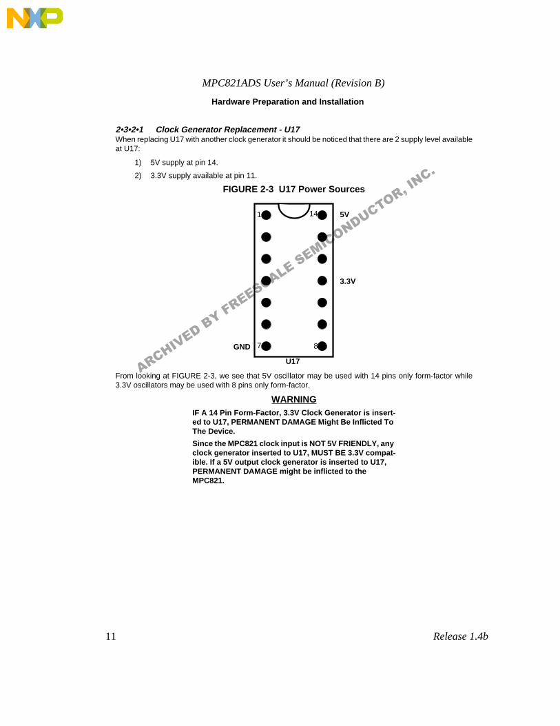
2•3•2•1 Clock Generator Replacement - U17
When replacing U17 with another clock generator it should be noticed that there are 2 supply level availableat U17:
1) 5V supply at pin 14.
2) 3.3V supply available at pin 11.
FIGURE 2-3 U17 Power Sources
From looking at FIGURE 2-3, we see that 5V oscillator may be used with 14 pins only form-factor while3.3V oscillators may be used with 8 pins only form-factor.
WARNING
IF A 14 Pin Form-Factor, 3.3V Clock Generator is insert-ed to U17, PERMANENT DAMAGE Might Be Inflicted To The Device.
Since the MPC821 clock input is NOT 5V FRIENDLY, any clock generator inserted to U17, MUST BE 3.3V compat-ible. If a 5V output clock generator is inserted to U17, PERMANENT DAMAGE might be inflicted to the MPC821.
GND
3.3V
5V1
7 8
14
U17ARCHIVED BY FREESCALE SEMICONDUCTOR, IN
C.
MPC821ADS User’s Manual (Revision B)
12
Release 1.4b
Hardware Preparation and Installation
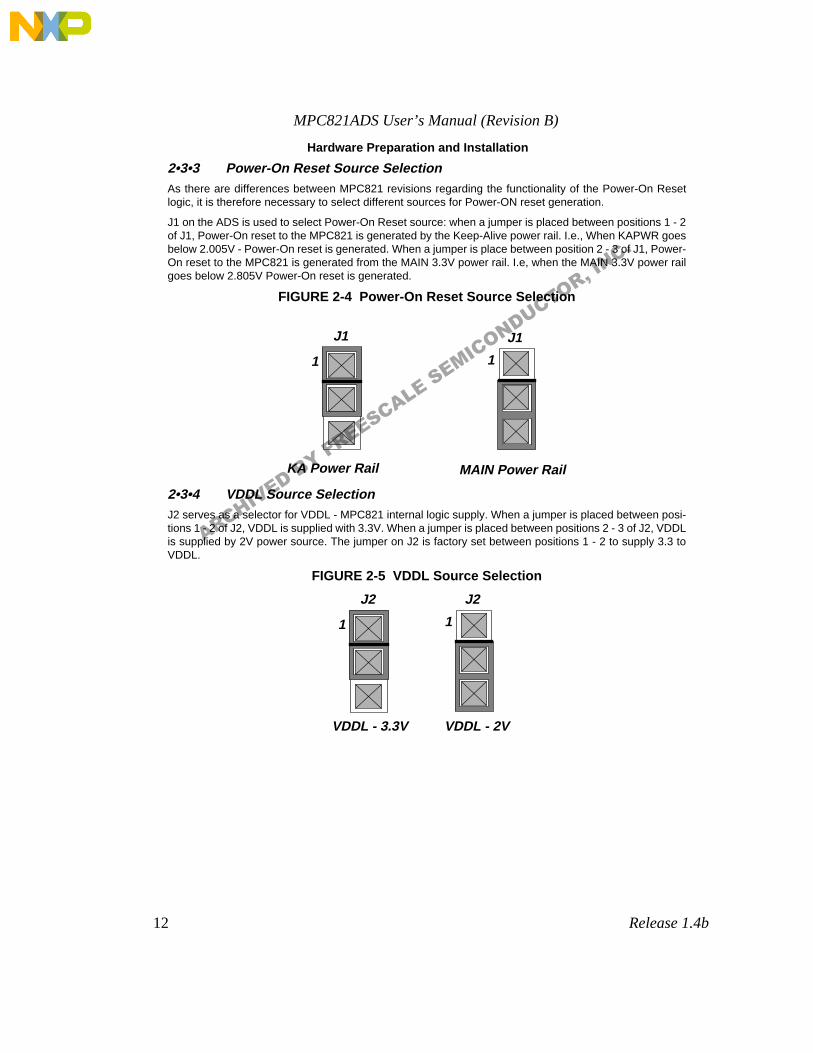
2•3•3 Power-On Reset Source Selection
As there are differences between MPC821 revisions regarding the functionality of the Power-On Resetlogic, it is therefore necessary to select different sources for Power-ON reset generation.
J1 on the ADS is used to select Power-On Reset source: when a jumper is placed between positions 1 - 2of J1, Power-On reset to the MPC821 is generated by the Keep-Alive power rail. I.e., When KAPWR goesbelow 2.005V - Power-On reset is generated. When a jumper is place between position 2 - 3 of J1, Power-On reset to the MPC821 is generated from the MAIN 3.3V power rail. I.e, when the MAIN 3.3V power railgoes below 2.805V Power-On reset is generated.
FIGURE 2-4 Power-On Reset Source Selection
2•3•4 VDDL Source Selection
J2 serves as a selector for VDDL - MPC821 internal logic supply. When a jumper is placed between posi-tions 1 - 2 of J2, VDDL is supplied with 3.3V. When a jumper is placed between positions 2 - 3 of J2, VDDLis supplied by 2V power source. The jumper on J2 is factory set between positions 1 - 2 to supply 3.3 toVDDL.
FIGURE 2-5 VDDL Source Selection
1 1
J1 J1
KA Power Rail MAIN Power Rail
1 1
VDDL - 3.3V VDDL - 2V
J2 J2
ARCHIVED BY FREESCALE SEMICONDUCTOR, INC.
MPC821ADS User’s Manual (Revision B)
13
Release 1.4b
Hardware Preparation and Installation
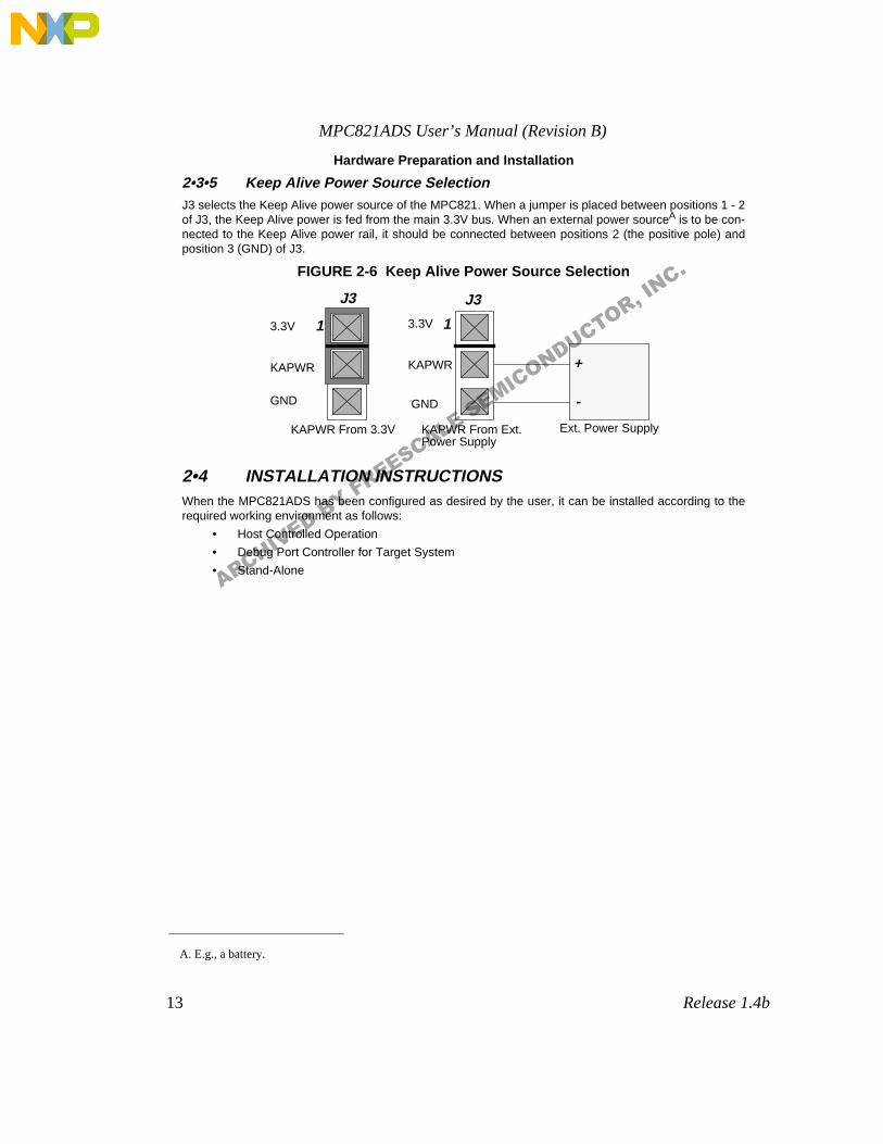
2•3•5 Keep Alive Power Source Selection
J3 selects the Keep Alive power source of the MPC821. When a jumper is placed between positions 1 - 2of J3, the Keep Alive power is fed from the main 3.3V bus. When an external power source
A
is to be con-nected to the Keep Alive power rail, it should be connected between positions 2 (the positive pole) andposition 3 (GND) of J3.
FIGURE 2-6 Keep Alive Power Source Selection
2•4 INSTALLATION INSTRUCTIONS
When the MPC821ADS has been configured as desired by the user, it can be installed according to therequired working environment as follows:
• Host Controlled Operation
• Debug Port Controller for Target System
• Stand-Alone
A. E.g., a battery.
1 1
J3 J3
+
-
Ext. Power Supply
3.3V
KAPWR
GND
3.3V
KAPWR
GND
KAPWR From 3.3V KAPWR From Ext.Power Supply
ARCHIVED BY FREESCALE SEMICONDUCTOR, INC.
MPC821ADS User’s Manual (Revision B)
14
Release 1.4b
Hardware Preparation and Installation
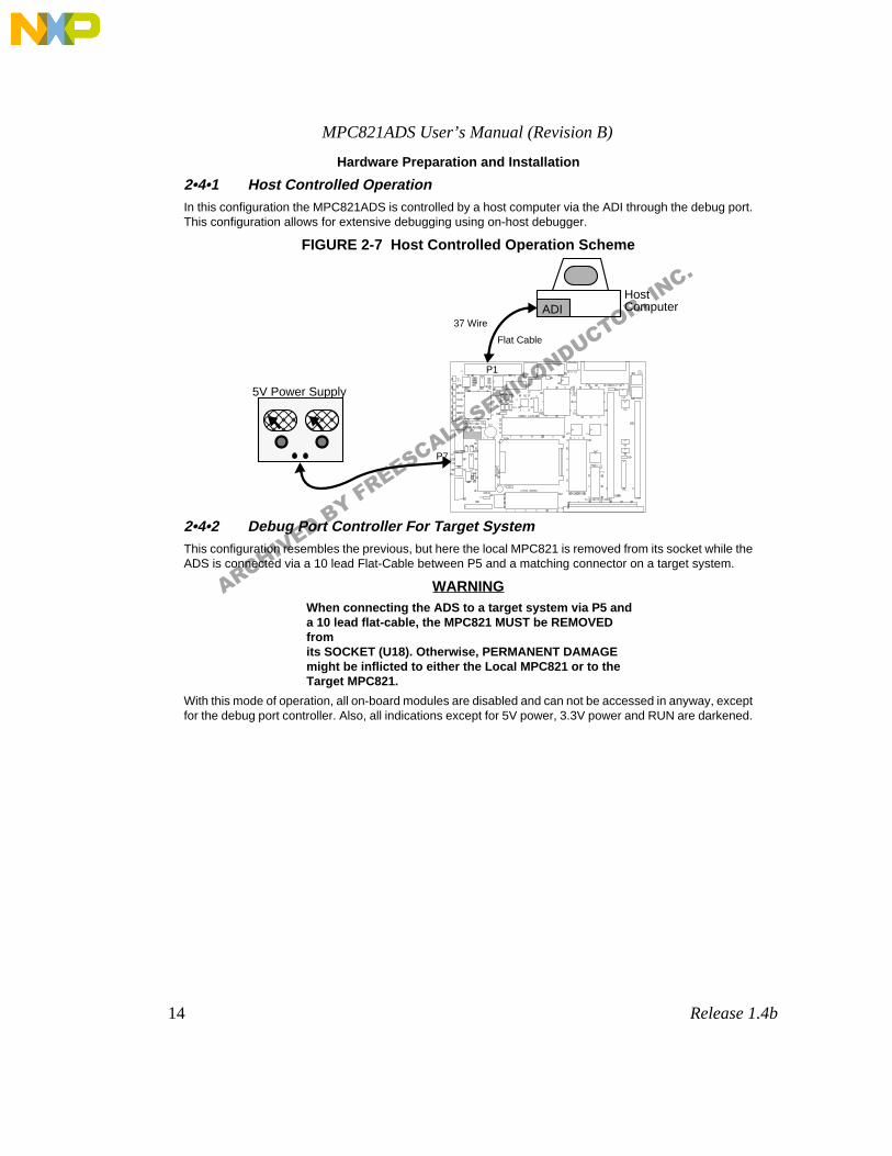
2•4•1 Host Controlled Operation
In this configuration the MPC821ADS is controlled by a host computer via the ADI through the debug port.This configuration allows for extensive debugging using on-host debugger.
FIGURE 2-7 Host Controlled Operation Scheme
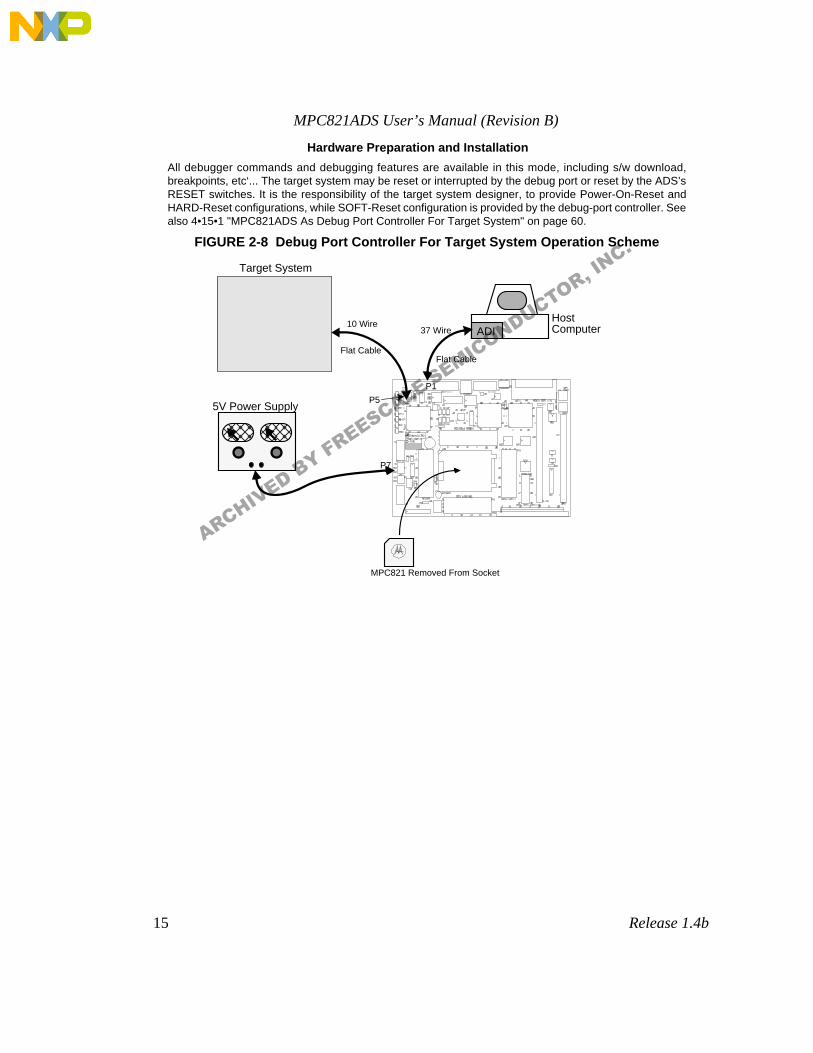
2•4•2 Debug Port Controller For Target System
This configuration resembles the previous, but here the local MPC821 is removed from its socket while theADS is connected via a 10 lead Flat-Cable between P5 and a matching connector on a target system.
WARNING
When connecting the ADS to a target system via P5 and a 10 lead flat-cable, the MPC821 MUST be REMOVED from its SOCKET (U18). Otherwise, PERMANENT DAMAGE might be inflicted to either the Local MPC821 or to the Target MPC821.
With this mode of operation, all on-board modules are disabled and can not be accessed in anyway, exceptfor the debug port controller. Also, all indications except for 5V power, 3.3V power and RUN are darkened.
Host Computer
5V Power Supply
ADI37 Wire
Flat Cable
P1
P7
ARCHIVED BY FREESCALE SEMICONDUCTOR, INC.
MPC821ADS User’s Manual (Revision B)
15
Release 1.4b
Hardware Preparation and Installation
All debugger commands and debugging features are available in this mode, including s/w download,breakpoints, etc‘... The target system may be reset or interrupted by the debug port or reset by the ADS’sRESET switches. It is the responsibility of the target system designer, to provide Power-On-Reset andHARD-Reset configurations, while SOFT-Reset configuration is provided by the debug-port controller. Seealso 4•15•1 "MPC821ADS As Debug Port Controller For Target System" on page 60.
FIGURE 2-8 Debug Port Controller For Target System Operation Scheme
Host Computer
5V Power Supply
ADI37 Wire
Flat Cable
P1
P7
Target System
10 Wire
Flat Cable
MPC821 Removed From Socket
P5
ARCHIVED BY FREESCALE SEMICONDUCTOR, INC.
MPC821ADS User’s Manual (Revision B)
16 Release 1.4b
Hardware Preparation and Installation
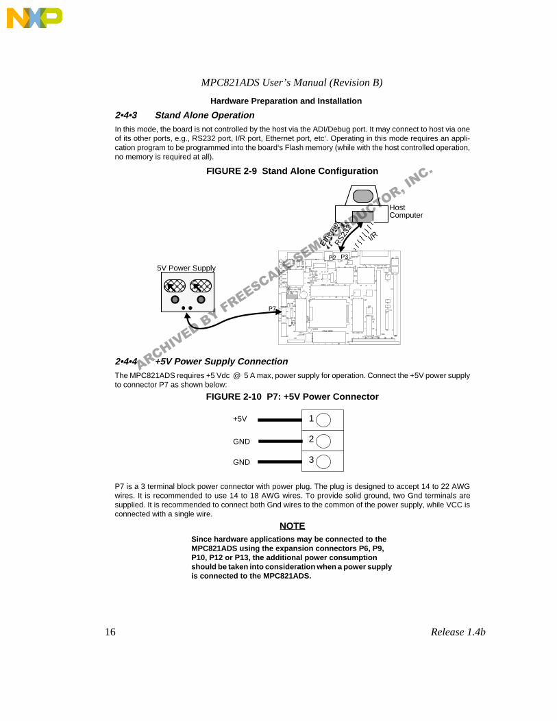
2•4•3 Stand Alone OperationIn this mode, the board is not controlled by the host via the ADI/Debug port. It may connect to host via oneof its other ports, e.g., RS232 port, I/R port, Ethernet port, etc‘. Operating in this mode requires an appli-cation program to be programmed into the board‘s Flash memory (while with the host controlled operation,no memory is required at all).
FIGURE 2-9 Stand Alone Configuration
2•4•4 +5V Power Supply ConnectionThe MPC821ADS requires +5 Vdc @ 5 A max, power supply for operation. Connect the +5V power supplyto connector P7 as shown below:
FIGURE 2-10 P7: +5V Power Connector
P7 is a 3 terminal block power connector with power plug. The plug is designed to accept 14 to 22 AWGwires. It is recommended to use 14 to 18 AWG wires. To provide solid ground, two Gnd terminals aresupplied. It is recommended to connect both Gnd wires to the common of the power supply, while VCC isconnected with a single wire.
NOTESince hardware applications may be connected to the MPC821ADS using the expansion connectors P6, P9, P10, P12 or P13, the additional power consumption should be taken into consideration when a power supply is connected to the MPC821ADS.
Host Computer
5V Power Supply
RS2
32
Ethe
rnet
I/R
P3P2
P7
+5V
GND
GND
1
2
3
ARCHIVED BY FREESCALE SEMICONDUCTOR, INC.
MPC821ADS User’s Manual (Revision B)
17 Release 1.4b
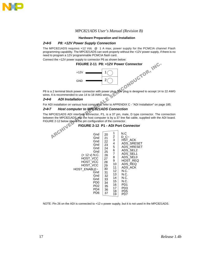
Hardware Preparation and Installation
2•4•5 P8: +12V Power Supply ConnectionThe MPC821ADS requires +12 Vdc @ 1 A max, power supply for the PCMCIA channel Flashprogramming capability. The MPC821ADS can work properly without the +12V power supply, if there is noneed to program a 12V programmable PCMCIA flash card.
Connect the +12V power supply to connector P6 as shown below:
FIGURE 2-11 P8: +12V Power Connector
P8 is a 2 terminal block power connector with power plug. The plug is designed to accept 14 to 22 AWGwires. It is recommended to use 14 to 18 AWG wires.
2•4•6 ADI InstallationFor ADI installation on various host computers, refer to APPENDIX C - "ADI Installation" on page 185.
2•4•7 Host computer to MPC821ADS ConnectionThe MPC821ADS ADI interface connector, P1, is a 37 pin, male, D type connector. The connectionbetween the MPC821ADS and the host computer is by a 37 line flat cable, supplied with the ADI board.FIGURE 2-12 below shows the pin configuration of the connector.
FIGURE 2-12 P1 - ADI Port Connector
NOTE: Pin 26 on the ADI is connected to +12 v power supply, but it is not used in the MPC821ADS.
+12V
GND
1
2
Gnd 20 N.C12Gnd 21
Gnd 22Gnd 23Gnd 24Gnd 25
(+ 12 v) N.C. 26
HST_ACK3ADS_SRESET4
HOST_VCC
ADS_HRESETADS_SEL2ADS_SEL1ADS_SEL0
567827
HOST_VCCHOST_VCC
GndGnd
HOST_ENABLE~
HOST_REQADS_REQADS_ACKN.C.N.C.N.C.
91011121314
2829303132
Gnd 33PD0 34PD2PD4PD6
N.C.PD1PD3PD5PD7
1516171819
353637
D_C~ARCHIVED BY FREESCALE SEMICONDUCTOR, INC.
MPC821ADS User’s Manual (Revision B)
18 Release 1.4b
Hardware Preparation and Installation
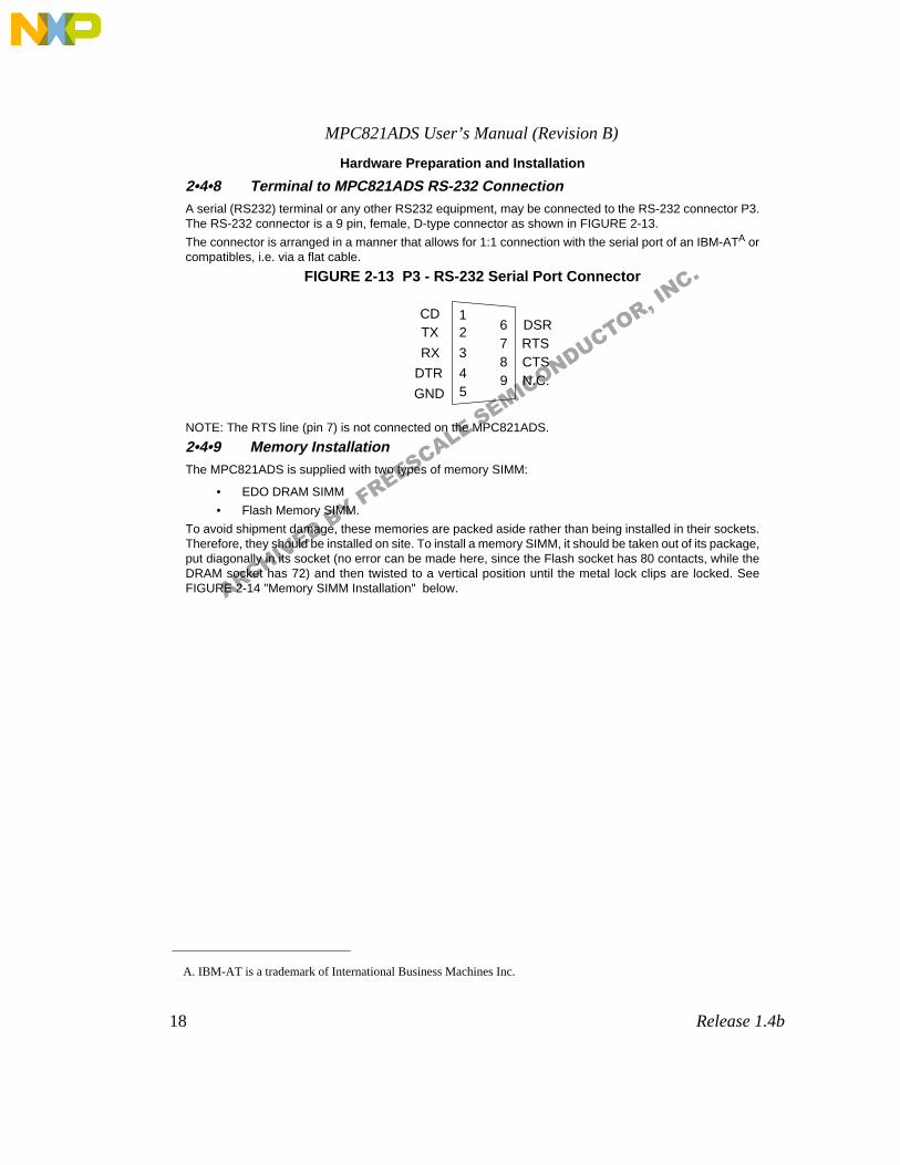
2•4•8 Terminal to MPC821ADS RS-232 ConnectionA serial (RS232) terminal or any other RS232 equipment, may be connected to the RS-232 connector P3.The RS-232 connector is a 9 pin, female, D-type connector as shown in FIGURE 2-13.
The connector is arranged in a manner that allows for 1:1 connection with the serial port of an IBM-ATA orcompatibles, i.e. via a flat cable.
FIGURE 2-13 P3 - RS-232 Serial Port Connector
NOTE: The RTS line (pin 7) is not connected on the MPC821ADS.
2•4•9 Memory InstallationThe MPC821ADS is supplied with two types of memory SIMM:
• EDO DRAM SIMM
• Flash Memory SIMM.
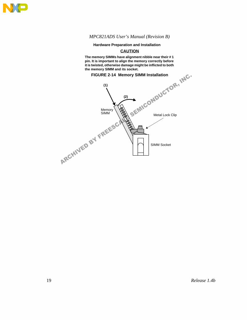
To avoid shipment damage, these memories are packed aside rather than being installed in their sockets.Therefore, they should be installed on site. To install a memory SIMM, it should be taken out of its package,put diagonally in its socket (no error can be made here, since the Flash socket has 80 contacts, while theDRAM socket has 72) and then twisted to a vertical position until the metal lock clips are locked. SeeFIGURE 2-14 "Memory SIMM Installation" below.
A. IBM-AT is a trademark of International Business Machines Inc.
1TX 2
RX 3RTS
4CTS
5
DSR6
GND
7
CD
89 N.C.DTR
ARCHIVED BY FREESCALE SEMICONDUCTOR, INC.
MPC821ADS User’s Manual (Revision B)
19 Release 1.4b
Hardware Preparation and Installation
CAUTIONThe memory SIMMs have alignment nibble near their # 1 pin. It is important to align the memory correctly before it is twisted, otherwise damage might be inflicted to both the memory SIMM and its socket.
FIGURE 2-14 Memory SIMM Installation
(1)
(2)
SIMM Socket
Memory SIMM Metal Lock Clip
ARCHIVED BY FREESCALE SEMICONDUCTOR, INC.
MPC821ADS User’s Manual (Revision B)
20 Release 1.4b
OPERATING INSTRUCTIONS
3 - OPERATING INSTRUCTIONS
3•1 INTRODUCTIONThis chapter provides necessary information to use the MPC821ADS in host-controlled and stand-aloneconfigurations. This includes controls and indicators, memory map details, and software initialization of theboard.
3•2 CONTROLS AND INDICATORSThe MPC821ADS has the following switches and indicators.
3•2•1 SOFT RESET Switch SW1The SOFT RESET switch SW1 performs Soft reset to the MPC821 internal modules, maintainingMPC821’s configuration (clocks & chip-selects) and dram contents. The switch signal is debounced, andit is not possible to disable it by software. At the end of the Soft Reset Sequence, the Soft ResetConfiguration is sampled and becomes valid.
3•2•2 ABORT Switch SW2The ABORT switch is normally used to abort program execution, this by issuing a level 0 interrupt to theMPC821. If the ADS is in stand alone modeA, it is the responsibility of the user to provide means of handlingthe interrupt, since there is no resident debugger with the MPC821ADS. The ABORT switch signal isdebounced, and can not be disabled by software.
3•2•3 HARD RESET - Switches SW1 & SW2When BOTH switches - SW1 and SW2 are depressed simultaneously, HARD reset is generated to theMPC821. When the MPC821 is HARD reset, all its configuration is lost, including data stored in the DRAMand the MPC821 has to be re-initialized. At the end of the Hard Reset sequence, the Hard ResetConfiguration stored in BCSR0 becomes valid.
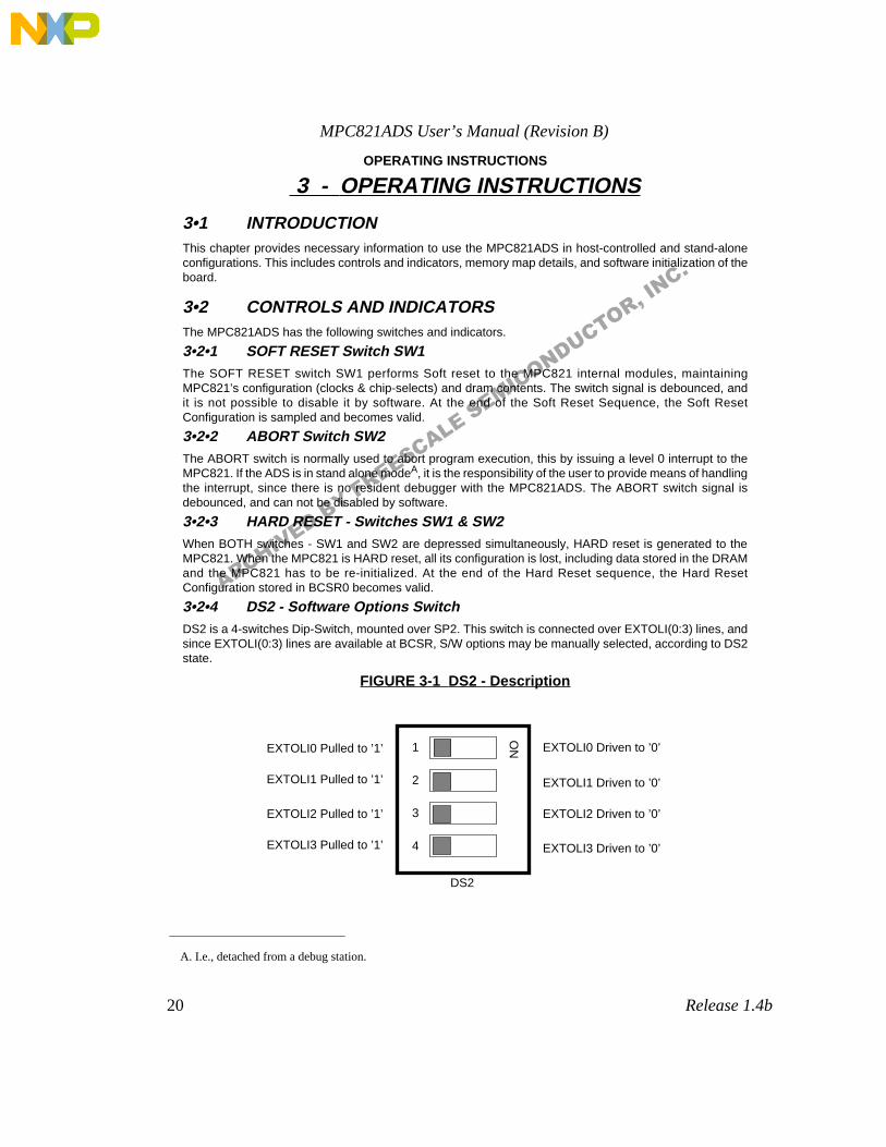
3•2•4 DS2 - Software Options SwitchDS2 is a 4-switches Dip-Switch, mounted over SP2. This switch is connected over EXTOLI(0:3) lines, andsince EXTOLI(0:3) lines are available at BCSR, S/W options may be manually selected, according to DS2state.
FIGURE 3-1 DS2 - Description
A. I.e., detached from a debug station.
DS2
ON1
2
3
4
EXTOLI0 Driven to ’0’
EXTOLI1 Driven to ’0’
EXTOLI2 Driven to ’0’
EXTOLI3 Driven to ’0’
EXTOLI0 Pulled to ’1’
EXTOLI1 Pulled to ’1’
EXTOLI2 Pulled to ’1’
EXTOLI3 Pulled to ’1’
ARCHIVED BY FREESCALE SEMICONDUCTOR, INC.
MPC821ADS User’s Manual (Revision B)
21 Release 1.4b
OPERATING INSTRUCTIONS
3•2•5 J4 Power BridgeJ4 is a soldered jumper, which is in series with the 3.3V power bus. This jumper may be removedA if currentmeasurements on the 3.3V bus are to be held.
WarningThere are also GND bridges on board, which physically resemble J4. Do not mistake J4 to be a GND jumper, oth-erwise, permanent damage might be inflicted to the MPC821ADS.
3•2•6 GND BridgesThere are 4 GND bridges on the MPC821ADS. They are meant to assist general measurements and logic-analyzer connection.
WarningWhen connecting to a GND bridge, use only INSULATED GND clips. Failure in doing so, might result in perma-nent damage to the MPC821ADS.
3•2•7 RUN Indicator - LD1When the green RUN led - LD1 is lit, it indicates that the MPC821 is not in debug mode, i.e., VFLS0 &VFLS1 == 0. It is important to remember, that if the VFLS(0:1) pins are programmed for alternative userather than function as VFLS lines, this indication is meaningless.
3•2•8 FLASH ON - LD2When the yellow FLASH ON led is lit, it indicates that the FLASH module is enabled in the BCSR1 register.I.e., any access done to the CS0~ address space will hit the flash memory. When it is dark, the flash isdisabled and CS0~ may be used off-board via the expansion connectors.
3•2•9 DRAM ON - LD3When the yellow DRAM ON led is lit, it indicates the DRAM is enabled in BCSR1. Therefore, any accessmade to CS1~ (or CS2~) will hit on the DRAM. When it is dark, it indicates that either the DRAM is disabledin BCSR1, enabling the use of CS1~ and CS2~ off-board via the expansion connectors.
3•2•10 ETH ON - LD4When the yellow ETH ON led is lit, it indicates that the ethernet port transceiver - the MC68160 EEST,connected to SCC1 is active. When it is dark, it indicates that the EEST is in power down mode, enablingthe use of SCC1 pins off-board via the expansion connectors.
3•2•11 Ethernet RX Indicator - LD5The green Ethernet Receive LED indicator blinks whenever the EEST is receiving data from one of theEthernet port.
3•2•12 Ethernet TX Indicator - LD6The green Ethernet Receive LED indicator blinks whenever the EEST is transmitting data via the Ethernetport.
3•2•13 Ethernet JABB Indicator - LD7The red Ethernet TP Jabber LED indicator - JABB, lights whenever a jabber condition is detected on theTP ethernet port.
A. By a skilled technician only.
ARCHIVED BY FREESCALE SEMICONDUCTOR, INC.
MPC821ADS User’s Manual (Revision B)
22 Release 1.4b
OPERATING INSTRUCTIONS
3•2•14 IRD ON - LD8When the yellow IRD ON led is lit, it indicates that the Infra-Red transceiver - the TFDS3000, connected toSCC2, is active and enables communication via that medium. When it is dark, the I/R transceiver is inshutdown mode, enabling the use of SCC2 pins off-board via the expansion connectors.
3•2•15 Ethernet CLSN Indicator LD9The red Ethernet Collision LED indicator CLSN, blinks whenever a collision condition is detected on theethernet port, i.e., simultaneous receive and transmit.
3•2•16 Ethernet PLR Indicator - LD10The red Ethernet TP Polarity LED indicator - PLR, lights whenever the wires connected to the receiver inputof the ethernet port are reversed. The LED is lit by the EEST, and remains on while the EEST hasautomatically corrected for the reversed wires.
3•2•17 Ethernet LIL Indicator - LD11The yellow Ethernet Twisted Pair Link Integrity LED indicator - LIL, lights to indicate good link integrity onthe TP port. The LED is off when the link integrity fails.
3•2•18 RS232 Port 1 ON - LD12When the yellow RS232 ON led is lit, it designates that the RS232 transceiver connected to SMC1, is activeand communication via that medium (through PA3) is allowed. When dark, it designates that thetransceiver is in shutdown mode, so SMC1 pins may be used off-board via the expansion connectors.
3•2•19 PCMCIA ON - LD13When the yellow PCMCIA ON led is lit, it indicates the following:
1) Address & strobe buffers are driven towards the PCMCIA card
2) Data buffers may be driven to / from the PCMCIA card depending on the CE1A~ and CE2A~ signals and transfer direction.
3) Card status lines are driven towards the MPC821 from the PCMCIA card.
When it is dark, it indicates that all the above buffers are tri-stated and the pins associated with PCMCIAchannel A, may be used off-board via the expansion connectors.
3•2•20 RS232 Port 2 ON - LD14When the yellow RS232 Port 2 ON led is lit, it designates that the RS232 transceiver connected to SMC2,is active and communication via that medium (through PB3) is allowed. When dark, it designates that thetransceiver is in shutdown mode, so SMC2 pins may be used off-board via the expansion connectors.
3•2•21 5V Indicator - LD15The yellow 5V led, indicates the presence of the +5V supply at P7.
3•2•22 3.3V Indicator - LD16The yellow 3.3V led indicates that the 3.3V power bus is powered
ARCHIVED BY FREESCALE SEMICONDUCTOR, INC.
MPC821ADS User’s Manual (Revision B)
23 Release 1.4b
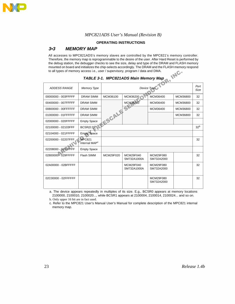
OPERATING INSTRUCTIONS
3•3 MEMORY MAPAll accesses to MPC821ADS’s memory slaves are controlled by the MPC821’s memory controller.Therefore, the memory map is reprogrammable to the desire of the user. After Hard Reset is performed bythe debug station, the debugger checks to see the size, delay and type of the DRAM and FLASH memorymounted on board and initializes the chip-selects accordingly. The DRAM and the FLASH memory respondto all types of memory access i.e., user / supervisory, program / data and DMA.
a. The device appears repeatedly in multiples of its size. E.g., BCSR0 appears at memory locations2100000, 2100010, 2100020..., while BCSR1 appears at 2100004, 2100014, 2100024... and so on.
b. Only upper 16 bit are in fact used.c. Refer to the MPC821 User’s Manual User’s Manual for complete description of the MPC821 internal
memory map.
TABLE 3-1. MPC821ADS Main Memory Map
ADDESS RANGE Memory Type Device TypePort Size
00000000 - 003FFFFF DRAM SIMM MCM36100 MCM36200 MCM36400 MCM36800 32
00400000 - 007FFFFF DRAM SIMM MCM36200 MCM36400 MCM36800 32
00800000 - 00FFFFFF DRAM SIMM MCM36400 MCM36800 32
01000000 - 01FFFFFF DRAM SIMM MCM36800 32
02000000 - 020FFFFF Empty Space
02100000 - 02103FFF BCSR(0:3)a 32b
02104000 - 021FFFFF Empty Space
02200000 - 02207FFF MPC821Internal MAPc
32
02208000 - 027FFFFF Empty Space
02800000 - 029FFFFF Flash SIMM MCM29F020 MCM29F040SM732A1000A
MCM29F080SM732A2000
32
02A00000 - 02BFFFFF MCM29F040SM732A1000A
MCM29F080SM732A2000
32
02C00000 - 02FFFFFF MCM29F080SM732A2000
32
ARCHIVED BY FREESCALE SEMICONDUCTOR, INC.
MPC821ADS User’s Manual (Revision B)
24 Release 1.4b
OPERATING INSTRUCTIONS
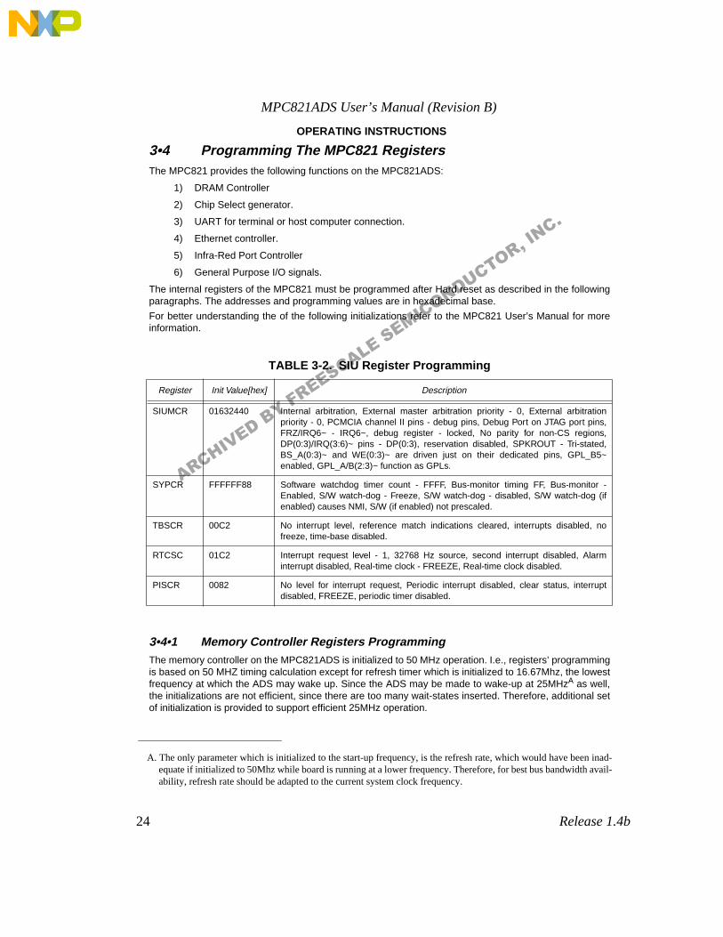
3•4 Programming The MPC821 RegistersThe MPC821 provides the following functions on the MPC821ADS:
1) DRAM Controller
2) Chip Select generator.
3) UART for terminal or host computer connection.
4) Ethernet controller.
5) Infra-Red Port Controller
6) General Purpose I/O signals.
The internal registers of the MPC821 must be programmed after Hard reset as described in the followingparagraphs. The addresses and programming values are in hexadecimal base.
For better understanding the of the following initializations refer to the MPC821 User’s Manual for moreinformation.
3•4•1 Memory Controller Registers ProgrammingThe memory controller on the MPC821ADS is initialized to 50 MHz operation. I.e., registers’ programmingis based on 50 MHZ timing calculation except for refresh timer which is initialized to 16.67Mhz, the lowestfrequency at which the ADS may wake up. Since the ADS may be made to wake-up at 25MHzA as well,the initializations are not efficient, since there are too many wait-states inserted. Therefore, additional setof initialization is provided to support efficient 25MHz operation.
A. The only parameter which is initialized to the start-up frequency, is the refresh rate, which would have been inad-equate if initialized to 50Mhz while board is running at a lower frequency. Therefore, for best bus bandwidth avail-ability, refresh rate should be adapted to the current system clock frequency.
TABLE 3-2. SIU Register Programming
Register Init Value[hex] Description
SIUMCR 01632440 Internal arbitration, External master arbitration priority - 0, External arbitrationpriority - 0, PCMCIA channel II pins - debug pins, Debug Port on JTAG port pins,FRZ/IRQ6~ - IRQ6~, debug register - locked, No parity for non-CS regions,DP(0:3)/IRQ(3:6)~ pins - DP(0:3), reservation disabled, SPKROUT - Tri-stated,BS_A(0:3)~ and WE(0:3)~ are driven just on their dedicated pins, GPL_B5~enabled, GPL_A/B(2:3)~ function as GPLs.
SYPCR FFFFFF88 Software watchdog timer count - FFFF, Bus-monitor timing FF, Bus-monitor -Enabled, S/W watch-dog - Freeze, S/W watch-dog - disabled, S/W watch-dog (ifenabled) causes NMI, S/W (if enabled) not prescaled.
TBSCR 00C2 No interrupt level, reference match indications cleared, interrupts disabled, nofreeze, time-base disabled.
RTCSC 01C2 Interrupt request level - 1, 32768 Hz source, second interrupt disabled, Alarminterrupt disabled, Real-time clock - FREEZE, Real-time clock disabled.
PISCR 0082 No level for interrupt request, Periodic interrupt disabled, clear status, interruptdisabled, FREEZE, periodic timer disabled.
ARCHIVED BY FREESCALE SEMICONDUCTOR, INC.
MPC821ADS User’s Manual (Revision B)
25 Release 1.4b
OPERATING INSTRUCTIONS
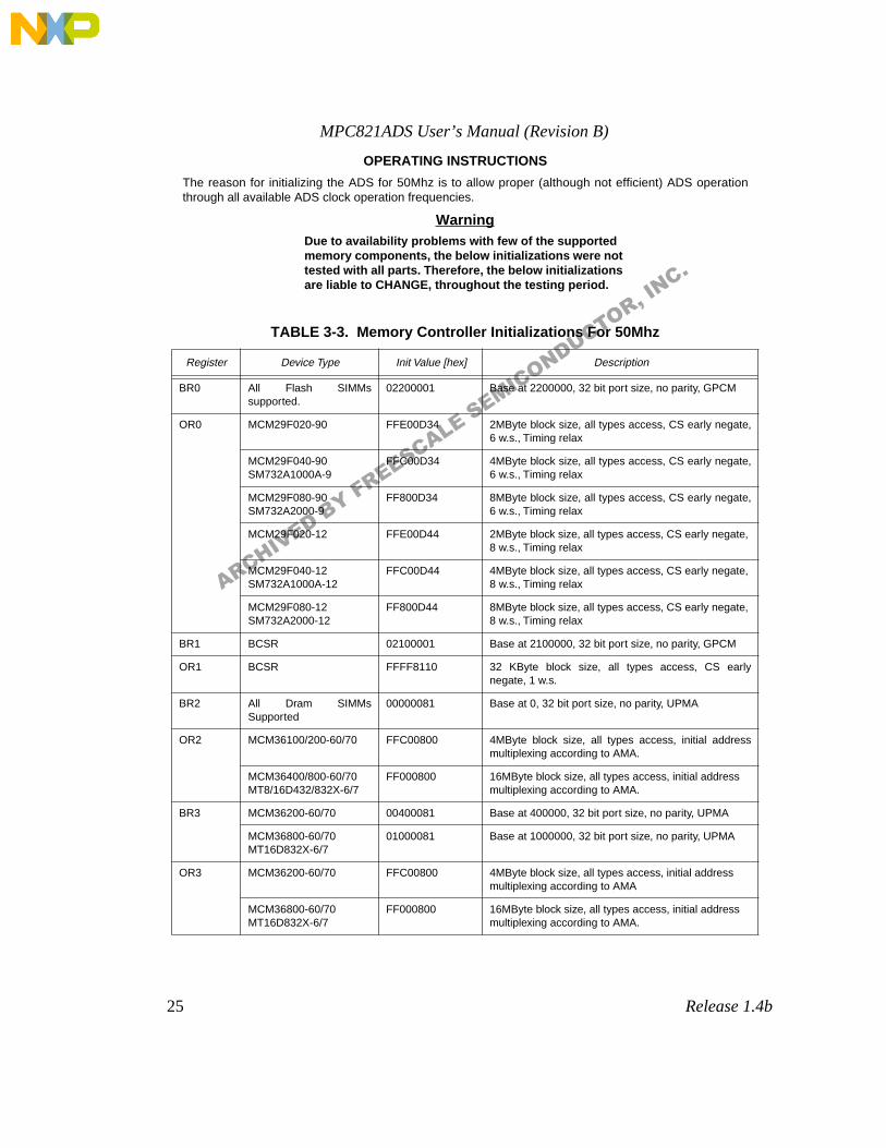
The reason for initializing the ADS for 50Mhz is to allow proper (although not efficient) ADS operationthrough all available ADS clock operation frequencies.
WarningDue to availability problems with few of the supported memory components, the below initializations were not tested with all parts. Therefore, the below initializations are liable to CHANGE, throughout the testing period.
TABLE 3-3. Memory Controller Initializations For 50Mhz
Register Device Type Init Value [hex] Description
BR0 All Flash SIMMssupported.
02200001 Base at 2200000, 32 bit port size, no parity, GPCM
OR0 MCM29F020-90 FFE00D34 2MByte block size, all types access, CS early negate,6 w.s., Timing relax
MCM29F040-90SM732A1000A-9
FFC00D34 4MByte block size, all types access, CS early negate,6 w.s., Timing relax
MCM29F080-90SM732A2000-9
FF800D34 8MByte block size, all types access, CS early negate,6 w.s., Timing relax
MCM29F020-12 FFE00D44 2MByte block size, all types access, CS early negate, 8 w.s., Timing relax
MCM29F040-12SM732A1000A-12
FFC00D44 4MByte block size, all types access, CS early negate, 8 w.s., Timing relax
MCM29F080-12SM732A2000-12
FF800D44 8MByte block size, all types access, CS early negate, 8 w.s., Timing relax
BR1 BCSR 02100001 Base at 2100000, 32 bit port size, no parity, GPCM
OR1 BCSR FFFF8110 32 KByte block size, all types access, CS earlynegate, 1 w.s.
BR2 All Dram SIMMsSupported
00000081 Base at 0, 32 bit port size, no parity, UPMA
OR2 MCM36100/200-60/70 FFC00800 4MByte block size, all types access, initial addressmultiplexing according to AMA.
MCM36400/800-60/70MT8/16D432/832X-6/7
FF000800 16MByte block size, all types access, initial address multiplexing according to AMA.
BR3 MCM36200-60/70 00400081 Base at 400000, 32 bit port size, no parity, UPMA
MCM36800-60/70MT16D832X-6/7
01000081 Base at 1000000, 32 bit port size, no parity, UPMA
OR3 MCM36200-60/70 FFC00800 4MByte block size, all types access, initial address multiplexing according to AMA
MCM36800-60/70MT16D832X-6/7
FF000800 16MByte block size, all types access, initial address multiplexing according to AMA.
ARCHIVED BY FREESCALE SEMICONDUCTOR, INC.
MPC821ADS User’s Manual (Revision B)
26 Release 1.4b
OPERATING INSTRUCTIONS
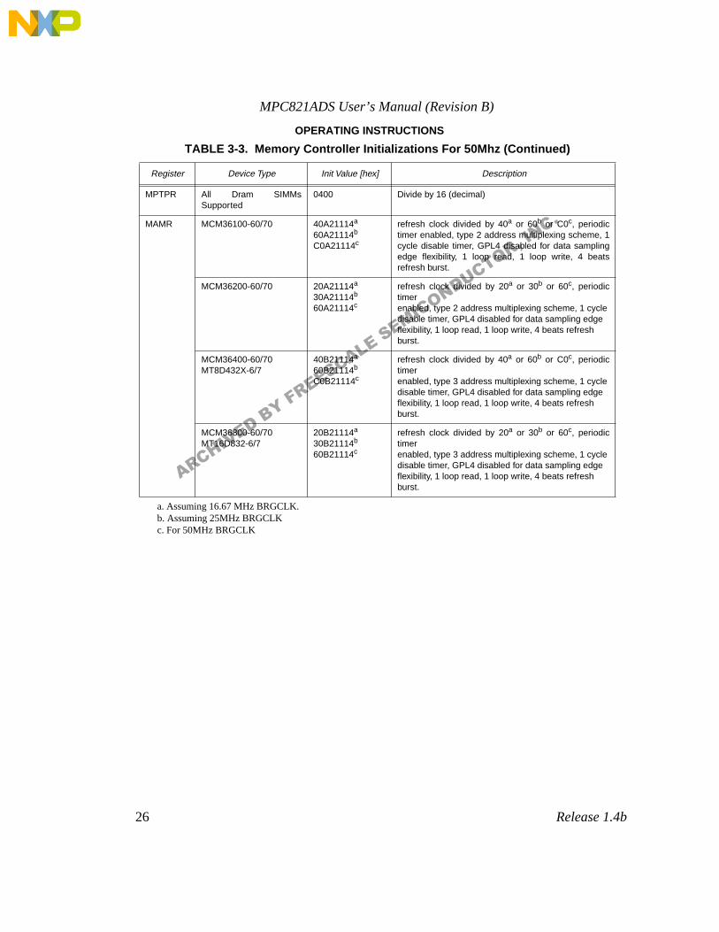
a. Assuming 16.67 MHz BRGCLK.b. Assuming 25MHz BRGCLKc. For 50MHz BRGCLK
MPTPR All Dram SIMMsSupported
0400 Divide by 16 (decimal)
MAMR MCM36100-60/70 40A21114a
60A21114b
C0A21114c
refresh clock divided by 40a or 60b or C0c, periodictimer enabled, type 2 address multiplexing scheme, 1cycle disable timer, GPL4 disabled for data samplingedge flexibility, 1 loop read, 1 loop write, 4 beatsrefresh burst.
MCM36200-60/70 20A21114a
30A21114b
60A21114c
refresh clock divided by 20a or 30b or 60c, periodictimer enabled, type 2 address multiplexing scheme, 1 cycle disable timer, GPL4 disabled for data sampling edge flexibility, 1 loop read, 1 loop write, 4 beats refresh burst.
MCM36400-60/70MT8D432X-6/7
40B21114a
60B21114b
C0B21114c
refresh clock divided by 40a or 60b or C0c, periodictimer enabled, type 3 address multiplexing scheme, 1 cycle disable timer, GPL4 disabled for data sampling edge flexibility, 1 loop read, 1 loop write, 4 beats refresh burst.
MCM36800-60/70MT16D832-6/7
20B21114a
30B21114b
60B21114c
refresh clock divided by 20a or 30b or 60c, periodictimer enabled, type 3 address multiplexing scheme, 1 cycle disable timer, GPL4 disabled for data sampling edge flexibility, 1 loop read, 1 loop write, 4 beats refresh burst.
TABLE 3-3. Memory Controller Initializations For 50Mhz (Continued)
Register Device Type Init Value [hex] Description
ARCHIVED BY FREESCALE SEMICONDUCTOR, INC.
MPC821ADS User’s Manual (Revision B)
27 Release 1.4b
OPERATING INSTRUCTIONS
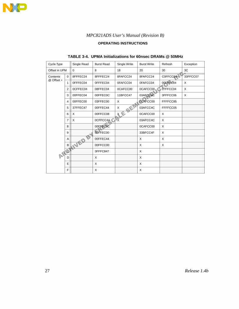
TABLE 3-4. UPMA Initializations for 60nsec DRAMs @ 50MHz
Cycle Type Single Read Burst Read Single Write Burst Write Refresh Exception
Offset in UPM 0 8 18 20 30 3C
Contents @ Offset +
0 8FFFEC24 8FFFEC24 8FAFCC24 8FAFCC24 C0FFCC84 33FFCC07
1 0FFFEC04 0FFFEC04 0FAFCC04 0FAFCC04 00FFCC04 X
2 0CFFEC04 08FFEC04 0CAFCC00 0CAFCC00 07FFCC04 X
3 00FFEC04 00FFEC0C 11BFCC47 03AFCC4C 3FFFCC06 X
4 00FFEC00 03FFEC00 X 0CAFCC00 FFFFCC85
5 37FFEC47 00FFEC44 X 03AFCC4C FFFFCC05
6 X 00FFCC08 X 0CAFCC00 X
7 X 0CFFCC44 X 03AFCC4C X
8 00FFEC0C 0CAFCC00 X
9 03FFEC00 33BFCC4F X
A 00FFEC44 X X
B 00FFCC00 X X
C 3FFFC847 X
D X X
E X X
F X X
ARCHIVED BY FREESCALE SEMICONDUCTOR, INC.
MPC821ADS User’s Manual (Revision B)
28 Release 1.4b
OPERATING INSTRUCTIONS
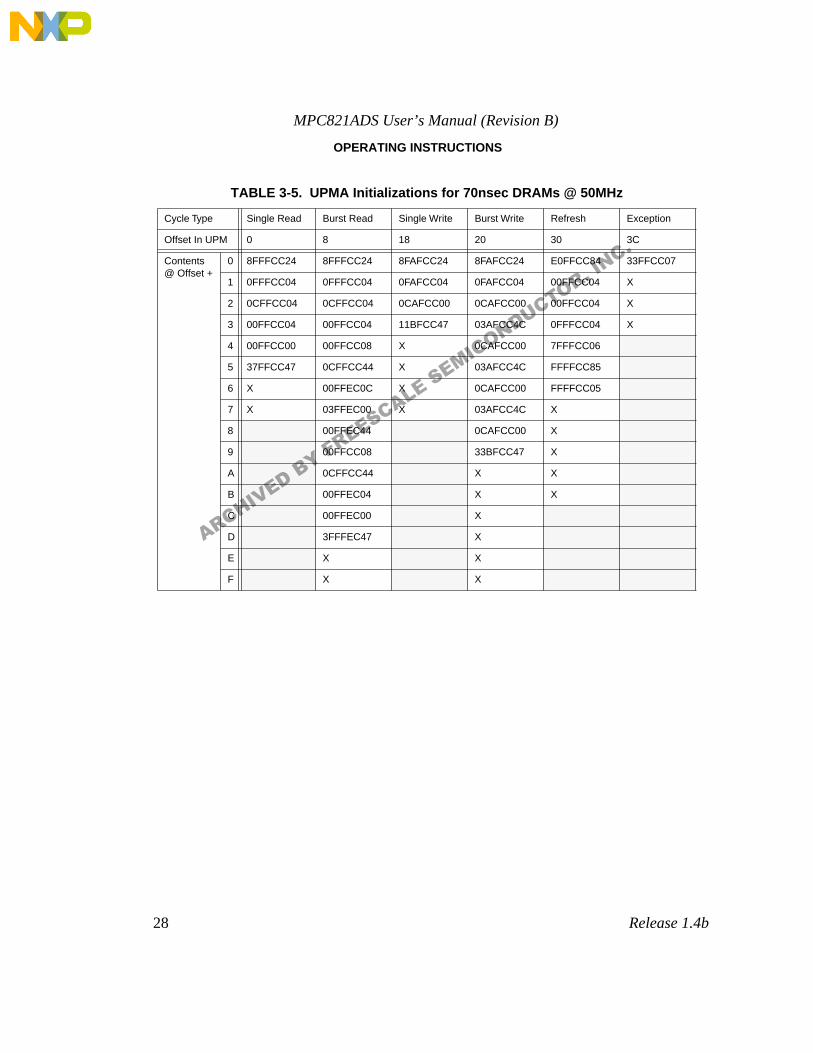
TABLE 3-5. UPMA Initializations for 70nsec DRAMs @ 50MHz
Cycle Type Single Read Burst Read Single Write Burst Write Refresh Exception
Offset In UPM 0 8 18 20 30 3C
Contents @ Offset +
0 8FFFCC24 8FFFCC24 8FAFCC24 8FAFCC24 E0FFCC84 33FFCC07
1 0FFFCC04 0FFFCC04 0FAFCC04 0FAFCC04 00FFCC04 X
2 0CFFCC04 0CFFCC04 0CAFCC00 0CAFCC00 00FFCC04 X
3 00FFCC04 00FFCC04 11BFCC47 03AFCC4C 0FFFCC04 X
4 00FFCC00 00FFCC08 X 0CAFCC00 7FFFCC06
5 37FFCC47 0CFFCC44 X 03AFCC4C FFFFCC85
6 X 00FFEC0C X 0CAFCC00 FFFFCC05
7 X 03FFEC00 X 03AFCC4C X
8 00FFEC44 0CAFCC00 X
9 00FFCC08 33BFCC47 X
A 0CFFCC44 X X
B 00FFEC04 X X
C 00FFEC00 X
D 3FFFEC47 X
E X X
F X X
ARCHIVED BY FREESCALE SEMICONDUCTOR, INC.

MPC821ADS User’s Manual (Revision B)
29 Release 1.4b
OPERATING INSTRUCTIONS
TABLE 3-6. UPMA Initializations for 60nsec EDO DRAMs @ 50MHz
Cycle Type Single Read Burst Read Single Write Burst Write Refresh Exception
Offset in UPM 0 8 18 20 30 3C
Contents @ Offset +
0 8FFBEC24 8FFFEC24 8FFFCC24 8FFFCC24 C0FFCC84 33FFCC07
1 0FF3EC04 0FFBEC04 0FEFCC04 0FEFCC04 00FFCC04 X
2 0CF3EC04 0CF3EC04 0CAFCC00 0CAFCC00 07FFCC04 X
3 00F3EC04 00F3EC0C 11BFCC47 03AFCC4C 3FFFCC06 X
4 00F3EC00 0CF3EC00 X 0CAFCC00 FFFFCC85
5 37F7EC47 00F3EC4C X 03AFCC4C FFFFCC05
6 X 0CF3EC00 X 0CAFCC00 X
7 X 00F3EC4C X 03AFCC4C X
8 0CF3EC00 0CAFCC00 X
9 00F3EC44 33BFCC4F X
A 03F3EC00 X X
B 3FF7EC47 X X
C X X
D X X
E X X
F X X
ARCHIVED BY FREESCALE SEMICONDUCTOR, INC.

MPC821ADS User’s Manual (Revision B)
30 Release 1.4b
OPERATING INSTRUCTIONS
TABLE 3-7. UPMA Initializations for 70nsec EDO DRAMs @ 50MHz
Cycle Type Single Read Burst Read Single Write Burst Write Refresh Exception
Offset In UPM 0 8 18 20 30 3C
Contents @ Offset +
0 8FFBCC24 8FFFCC24 8FFFCC24 8FFFCC24 E0FFCC84 33FFCC07
1 0FF3CC04 0FFBCC04 0FEFCC04 0FEFCC04 00FFCC04 X
2 0CF3CC04 0CF3CC04 0CAFCC00 0CAFCC00 00FFCC04 X
3 00F3CC04 00F3CC0C 11BFCC47 03AFCC4C 0FFFCC04 X
4 00F3CC00 03F3CC00 X 0CAFCC00 7FFFCC04
5 37F7CC47 00F3CC44 X 03AFCC4C FFFFCC86
6 X 00F3EC0C X 0CAFCC00 FFFFCC05
7 X 0CF3EC00 X 03AFCC4C X
8 00F3EC4C 0CAFCC00 X
9 03F3EC00 33BFCC47 X
A 00F3EC44 X X
B 00F3CC00 X X
C 33F7CC47 X
D X X
E X X
F X X
ARCHIVED BY FREESCALE SEMICONDUCTOR, INC.
MPC821ADS User’s Manual (Revision B)
31 Release 1.4b
OPERATING INSTRUCTIONS
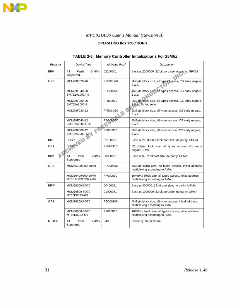
TABLE 3-8. Memory Controller Initializations For 25Mhz
Register Device Type Init Value [hex] Description
BR0 All Flash SIMMssupported.
02200001 Base at 2200000, 32 bit port size, no parity, GPCM
OR0 MCM29F020-90 FFE00D20 2MByte block size, all types access, CS early negate,2 w.s.
MCM29F040-90SM732A1000A-9
FFC00D20 4MByte block size, all types access, CS early negate,2 w.s.
MCM29F080-90SM732A2000-9
FF800920 8MByte block size, all types access, CS early negate,2 w.s., Timing relax
MCM29F020-12 FFE00D30 2MByte block size, all types access, CS early negate, 3 w.s.
MCM29F040-12SM732A1000A-12
FFC00D30 4MByte block size, all types access, CS early negate, 3 w.s.
MCM29F080-12SM732A2000-12
FF800930 8MByte block size, all types access, CS early negate, 3 w.s.
BR1 BCSR 02100001 Base at 2100000, 32 bit port size, no parity, GPCM
OR1 BCSR FFFF8110 32 KByte block size, all types access, CS earlynegate, 1 w.s.
BR2 All Dram SIMMsSupported
00000081 Base at 0, 32 bit port size, no parity, UPMA
OR2 MCM36100/200-60/70 FFC00800 4MByte block size, all types access, initial addressmultiplexing according to AMA.
MCM36400/800-60/70MT8/16D432/832X-6/7
FF000800 16MByte block size, all types access, initial address multiplexing according to AMA.
BR3a MCM36200-60/70 00400081 Base at 400000, 32 bit port size, no parity, UPMA
MCM36800-60/70MT16D832X-6/7
01000081 Base at 1000000, 32 bit port size, no parity, UPMA
OR3 MCM36200-60/70 FFC00800 4MByte block size, all types access, initial address multiplexing according to AMA
MCM36800-60/70MT16D832X-6/7
FF000800 16MByte block size, all types access, initial address multiplexing according to AMA.
MPTPR All Dram SIMMsSupported
0400 Divide by 16 (decimal)
ARCHIVED BY FREESCALE SEMICONDUCTOR, INC.
MPC821ADS User’s Manual (Revision B)
32 Release 1.4b
OPERATING INSTRUCTIONS
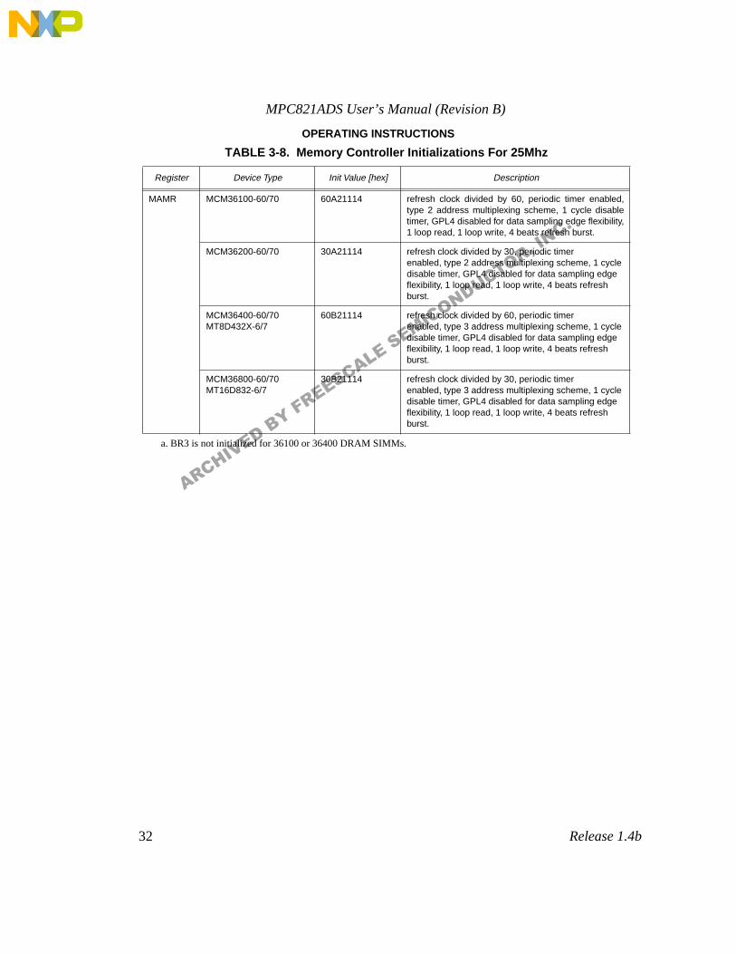
a. BR3 is not initialized for 36100 or 36400 DRAM SIMMs.
MAMR MCM36100-60/70 60A21114 refresh clock divided by 60, periodic timer enabled,type 2 address multiplexing scheme, 1 cycle disabletimer, GPL4 disabled for data sampling edge flexibility,1 loop read, 1 loop write, 4 beats refresh burst.
MCM36200-60/70 30A21114 refresh clock divided by 30, periodic timer enabled, type 2 address multiplexing scheme, 1 cycle disable timer, GPL4 disabled for data sampling edge flexibility, 1 loop read, 1 loop write, 4 beats refresh burst.
MCM36400-60/70MT8D432X-6/7
60B21114 refresh clock divided by 60, periodic timer enabled, type 3 address multiplexing scheme, 1 cycle disable timer, GPL4 disabled for data sampling edge flexibility, 1 loop read, 1 loop write, 4 beats refresh burst.
MCM36800-60/70MT16D832-6/7
30B21114 refresh clock divided by 30, periodic timer enabled, type 3 address multiplexing scheme, 1 cycle disable timer, GPL4 disabled for data sampling edge flexibility, 1 loop read, 1 loop write, 4 beats refresh burst.
TABLE 3-8. Memory Controller Initializations For 25Mhz
Register Device Type Init Value [hex] Description
ARCHIVED BY FREESCALE SEMICONDUCTOR, INC.
MPC821ADS User’s Manual (Revision B)
33 Release 1.4b
OPERATING INSTRUCTIONS
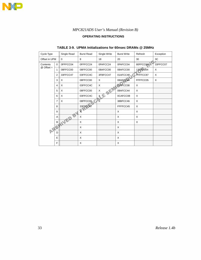
TABLE 3-9. UPMA Initializations for 60nsec DRAMs @ 25MHz
Cycle Type Single Read Burst Read Single Write Burst Write Refresh Exception
Offset in UPM 0 8 18 20 30 3C
Contents @ Offset +
0 0FFFCC04 0FFFCC24 0FAFCC24 0FAFCC04 80FFCC84 33FFCC07
1 08FFCC00 08FFCC00 08AFCC00 08AFCC00 13FFCC04 X
2 33FFCC47 03FFCC4C 3FBFCC47 01AFCC48 FFFFCC87 X
3 X 08FFCC00 X 08AFCC44 FFFFCC05 X
4 X 03FFCC4C X 0FAFCC08 X
5 X 08FFCC00 X 08AFCC44 X
6 X 03FFCC4C X 0CAFCC08 X
7 X 08FFCC00 X 38BFCC46 X
8 33FFCC47 FFFFCC45 X
9 X X X
A X X X
B X X X
C X X
D X X
E X X
F X X
ARCHIVED BY FREESCALE SEMICONDUCTOR, INC.
MPC821ADS User’s Manual (Revision B)
34 Release 1.4b
OPERATING INSTRUCTIONS
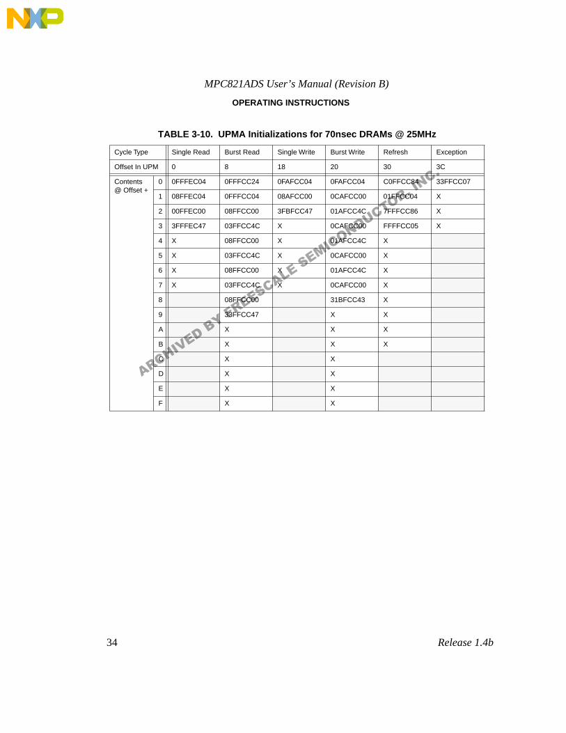
TABLE 3-10. UPMA Initializations for 70nsec DRAMs @ 25MHz
Cycle Type Single Read Burst Read Single Write Burst Write Refresh Exception
Offset In UPM 0 8 18 20 30 3C
Contents @ Offset +
0 0FFFEC04 0FFFCC24 0FAFCC04 0FAFCC04 C0FFCC84 33FFCC07
1 08FFEC04 0FFFCC04 08AFCC00 0CAFCC00 01FFCC04 X
2 00FFEC00 08FFCC00 3FBFCC47 01AFCC4C 7FFFCC86 X
3 3FFFEC47 03FFCC4C X 0CAFCC00 FFFFCC05 X
4 X 08FFCC00 X 01AFCC4C X
5 X 03FFCC4C X 0CAFCC00 X
6 X 08FFCC00 X 01AFCC4C X
7 X 03FFCC4C X 0CAFCC00 X
8 08FFCC00 31BFCC43 X
9 33FFCC47 X X
A X X X
B X X X
C X X
D X X
E X X
F X X
ARCHIVED BY FREESCALE SEMICONDUCTOR, INC.
MPC821ADS User’s Manual (Revision B)
35 Release 1.4b
OPERATING INSTRUCTIONS
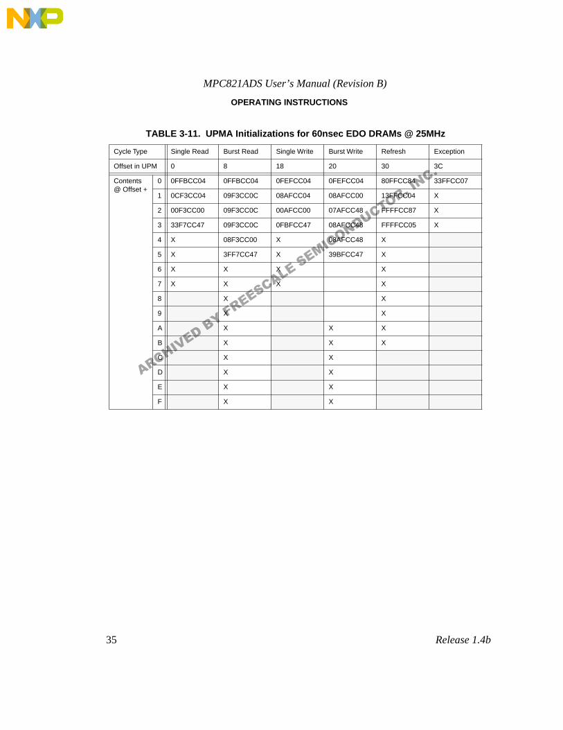
TABLE 3-11. UPMA Initializations for 60nsec EDO DRAMs @ 25MHz
Cycle Type Single Read Burst Read Single Write Burst Write Refresh Exception
Offset in UPM 0 8 18 20 30 3C
Contents @ Offset +
0 0FFBCC04 0FFBCC04 0FEFCC04 0FEFCC04 80FFCC84 33FFCC07
1 0CF3CC04 09F3CC0C 08AFCC04 08AFCC00 13FFCC04 X
2 00F3CC00 09F3CC0C 00AFCC00 07AFCC48 FFFFCC87 X
3 33F7CC47 09F3CC0C 0FBFCC47 08AFCC48 FFFFCC05 X
4 X 08F3CC00 X 08AFCC48 X
5 X 3FF7CC47 X 39BFCC47 X
6 X X X X
7 X X X X
8 X X
9 X X
A X X X
B X X X
C X X
D X X
E X X
F X X
ARCHIVED BY FREESCALE SEMICONDUCTOR, INC.

MPC821ADS User’s Manual (Revision B)
36 Release 1.4b
OPERATING INSTRUCTIONS
TABLE 3-12. UPMA Initializations for 70nsec EDO DRAMs @ 25MHz
Cycle Type Single Read Burst Read Single Write Burst Write Refresh Exception
Offset In UPM 0 8 18 20 30 3C
Contents@ Offset +
0 0FFBCC04 0FFBEC04 0FEFCC04 0FEFCC04 C0FFCC84 33FFCC07
1 0CF3CC04 08F3EC04 08AFCC04 08AFCC00 01FFCC04 X
2 00F3CC00 03F3EC48 00AFCC00 07AFCC4C 7FFFCC86 X
3 33F7CC47 08F3CC00 0FBFCC47 08AFCC00 FFFFCC05 X
4 X 0FF3CC4C X 07AFCC4C X
5 X 08F3CC00 X 08AFCC00 X
6 X 0FF3CC4C X 07AFCC4C X
7 X 08F3CC00 X 08AFCC00 X
8 3FF7CC47 37BFCC47 X
9 X X X
A X X X
B X X X
C X X
D X X
E X X
F X X
ARCHIVED BY FREESCALE SEMICONDUCTOR, INC.

MPC821ADS User’s Manual (Revision B)
37 Release 1.4b
Functional Description
4 - Functional DescriptionIn this chapter the various modules combining the MPC821ADS are described to their design details.
4•1 MPC821The MPC821 runs @ frequencies from 15A - 50 MHz and is buffered from the rest of the board’s logic - thisto allow for external hardware development via dedicated expansion connectors. P6, P9, P10 & P12.
4•2 Reset & Reset - ConfigurationThere are several reset sources on the MPC821ADS:
1) Keep Alive Power-On Reset
2) Main Power On Reset
3) Manual Soft-Reset
4) Manual Hard-Reset
5) Debug Port Soft-Reset
6) Debug Port Hard-Reset
7) MPC821 Internal Sources.
4•2•1 Keep Alive Power-On ResetThe Keep Alive Power - On Reset on the MPC821ADS is generated by a dedicated voltage detector madeby Seiko the S-8051HN-CD-X with detection voltage range of 1.795 to 2.005V. This voltage detector is con-nected to the Keep Alive power input of the MPC821 and during keep alive power-on or when there is avoltage drop of that input into the above range and J1 is set accordingly (see 2•3•3 "Power-On ResetSource Selection" on page 12), Power-On Reset is generated, i.e., PORESET* input of the MPC821 isasserted for a period of approximately 4 sec.
When PORESET* is asserted to the MPC821, the Power-On reset configuration is made available toMPC821. See 4•2•6•1 "Power - On Reset Configuration" on page 38.
4•2•2 Main Power - On ResetThe Main power on reset generates HARD reset and optionally PON reset, when the MAIN 3.3V bus ispowered-on or there is a drop of voltage level over this bus. The reset is generated by a dedicated voltagedetector made by Seiko the S-8052ANY-NH-X with detection voltage range of 2.595 to 2.805V. Whenregular power-on reset conditions exist, the HRESET* signal of the MPC821 is asserted for a period of ap-proximately 4 sec. In addition, if J1 is set accordingly (see 2•3•3 "Power-On Reset Source Selection" onpage 12), Power-On Reset is generated, i.e., PORESET* input of the MPC821 is asserted for a period ofapproximately 4 sec.
When HRESET signal is asserted, the HARD reset configuration is made available to the MPC821. See4•2•6•2 "Hard Reset Configuration" on page 38.
When PORESET* is asserted to the MPC821, the Power-On reset configuration is made available toMPC821. See 4•2•6•1 "Power - On Reset Configuration" on page 32.
A. The MPC821’s PLL minimal frequency is 15MHz. Below that, the Low-Power-Divider must be incorporated, dur-ing the operation of which, CLKOUT is no longer 50% duty-cycle, distorting UPM timing.
ARCHIVED BY FREESCALE SEMICONDUCTOR, INC.

MPC821ADS User’s Manual (Revision B)
38 Release 1.4b
Functional Description
4•2•3 Manual Soft ResetTo support resident application development and debuggers, a soft reset push-button is provided. De-pressing that button, asserts the SRESET* pin of the MPC821, generating a SOFT RESET sequence. Thisbutton is debounced to avoid spikes over the SRESET* line.
When SRESET* is signal is asserted, the SOFT reset configuration is made available to the MPC821. See4•2•6•3 "Soft Reset Configuration" on page 39.
4•2•4 Manual Hard ResetTo support resident application development, a hard reset push-button is providedA. When the soft resetpush-button is depressed in conjunction with the ABORT push-button, the HRESET* line is asserted, gen-erating a HARD RESET sequence. The button sharing is for economy and board space saving and doesnot effect in any way, functionality.
4•2•5 MPC821 Internal SourcesSince the HRESET* and SRESET* lines of the MPC821 are open-drain and the on-board reset logic drivesthese lines with open-drain gates, the correct operation of the internal reset sources of the MPC821 is fa-cilitated. As a rule, an internal reset source will assert HRESET* and / or SRESET* for a minimum time of512 system clocks. It is beyond the scope of this document to describe these sources, however Debug-Port Soft / Hard Resets which are part of the development support systemB, are regarded as such.
4•2•6 Reset ConfigurationDuring reset sequences to their kinds, the MPC821 device samples the state of some external pins to de-termine its operation modes and pin configuration. There are 3 kinds of reset levels to the MPC821, eachlevel having its own configuration sampled:
1) Power - On Reset configuration
2) Hard Reset configuration
3) Soft Reset Configuration.
4•2•6•1 Power - On Reset ConfigurationJust before PORESET* is negated by the external logic, the power-on reset configuration which includethe MODCK(1:2) pins is sampled. These pins determine the clock operation mode of the MPC821. Twoclock modes are supported within the MPC821ADS:
1) 1:5 PLL operation via on-board clock generator.
In this mode MODCK(1:2) are driven with ’11’ duringC power on reset.
2) 1:513 PLL operation via on-board clock generator.
In this mode MODCK(1:2) are driven with ’10’. during power-on reset.
4•2•6•2 Hard Reset ConfigurationDuring HARD reset sequence, when RSTCONF* pin is asserted, the data bus state is sampled to acquirethe MPC821’s hard reset configuration. The reset configuration word is driven by BCSR0 register, defaultsof which are set during power-on reset. The BCSR0 drives the half configuration word, i.e., data bitsD(0:15) in which the reserved bits are designated RSRVxx. If the hard-reset configuration is to bechangedD, BCSR0 may be written with new values, which become valid after HARD reset is applied to theADS.
A. It is not a dedicated button.B. And therefore mentioned.C. The MODCK lines are in fact driven longer - by HRESET~ line.D. With respect the ADS’s power-on defaults.
ARCHIVED BY FREESCALE SEMICONDUCTOR, INC.

MPC821ADS User’s Manual (Revision B)
39 Release 1.4b
Functional Description
On the MPC821ADS, the RSTCONF* line is always driven during HARD reset, i.e., no use is possible withthe MPC821’s internal HARD reset configuration defaults.
To allow user programmable, full-word hard reset configuration, i.e., D(0:31) lines being driven duringHARD reset, an option is provided for Flash memory driven hard reset configuration. I.e., the desired hard-reset configuration word is taken from the first word of the Flash memory. During hard-reset this worddrives the data bus to set the desired configuration. To support this option, CS0~ of the MPC821 shouldbe assertedA during HARD reset and the ADDRESS lines should be driven low. The selection of this optionis done via BCSR1. See TABLE 4-6. "BCSR1 Description" on page 53.
The system parameters to which BCSR0 defaults during power-on reset and are driven at hard-reset arelisted below:
1) Arbitration: internal arbitration is selected.
2) Interrupt Prefix: The internal default is interrupt prefix at 0xFFF00000. It is overridden to provide interrupt prefix at address 0, which is located within the DRAM.
3) Boot Disable: Boot is enabled.
4) Boot Port Size: 32 bit boot port size is selected.
5) Initial Internal Space Base: Immediately after HARD reset, the internal space is located at $FF000000.
6) Debug pins configuration: PCMCIA port B pins become debug support pinsB.
7) Debug port pins configuration. Debug port pins are on the JTAG port.
8) External Bus Division Factor: 1:1 internal to external clocks ratio is selected.
4•2•6•3 Soft Reset ConfigurationThe rising edge of SRESET* is used to configure the development port. Before the negation of SRESET*,DSCKC is sampled to determine for debug-mode enable / disable. After SRESET* is negated, if debugmode was enabled, DSCK is sampled again for debug-mode entry / non-entry.
DSDI is used to determine the debug port clock mode and is sampled after the negation of SRESET*.D
The Soft Reset configuration is provided by the debug-port controller U7 via the ADI I/F. When an ADIbundle is connected, i.e., a debug station is connected, debug mode is always enabled, while immediateentry is determined by the debug station. When a bundle is not connected to the ADI port, or disconnectedfrom the host computer, debug mode is disabled by means of pulling DSCK low via a pull-down resistor.
4•3 Local InterrupterThe only external interrupt applied to the MPC821 via its interrupt controller is the ABORT (NMI), which isgenerated by a push-button - SW2. When this button is depressed, the NMI input to the MPC821 isasserted (low). The purpose of this type of interrupt, is support the use of resident debuggers if any is madeavailable to the MPC821ADS. All other interrupts to the MPC821, are generated internally by theMPC821’s peripherals and by the debug port.
To support external (off-board) generation of an NMI, the IRQ0* line which drives the MPC821’s NMI, isdriven by an open-drain gate. This allows for external h/w to also drive this line. If an external h/w indeeddoes so, it is compulsory that IRQ0* is driven by an open-drain (or open-collector) gate.
A. May be supported on future revisions of the MPC821.B. I.e., AT, VF, VFLS...C. DSCK is configured at hard-reset to reside on the JTAG port.D. With parts from the MPC5XX family DSDI is sampled prior (3 system-clock cycles) to the negation of SRESET*,
to determine the part’s configuration source: internal (default) or external via data bus.
ARCHIVED BY FREESCALE SEMICONDUCTOR, INC.
MPC821ADS User’s Manual (Revision B)
40 Release 1.4b
Functional Description
4•4 Clock GeneratorThere are 2 ways to clock the MPC821 on the MPC821ADS:
1) 3 - 5MHz Clock generator connected to CLK4IN input. 1:5 PLL mode.
2) 32.768 KHz crystal resonator via EXTAL-XTAL pair of the MPC821, 1:513 initial PLL multiplica-tion factor.
The clock generator (1) above, is a 3.3V operated, or 5V operated with 3.3V compatible output.
The selection between the above modes is done using switch #4 of DS1. See 2•3•2 "Clock Source Selec-tion" on page 10. See also 4•2•6 "Reset Configuration" on page 38. DS1/4 has dual functionality: it is re-sponsible to the combination driven to the MODCK lines during power-on reset and to the connection ofthe appropriate capacitor between XFC and VDDSYN lines to match the PLL’s multiplication factor. When1:5 mode is selected, a capacitor of 5nF is connected, while when 1:513 mode is selected a 0.68µF capac-itor is connected parallel to it via a TMOS gate. The capacitors’ values are calculated to support a widerrange of multiplication factors as possible.
When mode (2) above is selected, the output of the clock generator is gated from CLK4IN and driven to ’0’constantly so that a jitter-free system clock is generated.
4•4•1 SPLL SupportSince the SPLL requires quiet supplies, GNDSYN and GNDSYN1have a dedicated ground plane connect-ed only in one point to the global ground plane of the ads. Bypassing capacitors pairs of 0.1µF and 0.01uFare connected as close as possible between VDDSYN and GNDSYN. VDDSYN is filtered from the digitalsupply using a LC filter with a double pole @ app. 500 hz to provide satisfactoryA attenuation of switchingregulators noise over PLL supply lines.
4•5 BufferingAs the MPC821ADS is meant to serve also as a hardware development platform, it is necessary to bufferthe MPC821 from the local bus, so the MPC821’s capacitive drive capability is not wasted internally andremains available for user’s off-board applications via the expansion connectors.
Since the total capacitive load over the address lines of all local memory slaves is significant, two parallelsets of buffers are provided for address - a dedicated group for the Flash memory and PCMCIA (U29, U33& U34) and a dedicated group for the DRAM (part of U30 and U32). Strobe lines are also buffered (U30,U35 & U37) while transceivers are provided for data (U39 - U42).
The data transceivers open only if there is an access to a validB board address or during Hard - Reset con-figurationC. That way data conflicts are avoided in case an off-board memory is read, provided that it is notmapped to an address valid on board. It is the users’ responsibility to avoid such errors.
4•6 Chip-Select GeneratorThe memory controller of the MPC821 is used as a chip-select generator to access on-boardD memories,saving board’s area reducing cost, power consumption and increasing flexibility. To enhance off-board ap-plication development, memory modules (including the BCSRx) may be disabled via BCSR1E in favor ofan external memory connected via the expansion connectors. That way, a CS line may be used off-boardvia the expansion connectors, while its associated local memory is disabled.
A. Approximately -45dB @ 5KHz.B. An address which is covered in a Chip-Select region and that CS region is enabled via BCSR1.C. To allow a configuration word stored in Flash memory become active.D. And off-board. See further.E. After the BCSR is removed from the local memory map, there is no way to access it but to remove and re-apply
power to the ADS.
ARCHIVED BY FREESCALE SEMICONDUCTOR, INC.

MPC821ADS User’s Manual (Revision B)
41 Release 1.4b
Functional Description
When a CS region is disabled via BCSR1, the local data transceivers are not open during access to thatregion, avoiding possibleA contention over data lines.
The MPC821’s chip-selects assignment to the various memories / registers on the MPC821ADS are asfollows:
1) CS0* - Flash memory
2) CS1* - BCSR
3) CS2* - DRAM Bank 1.
4) CS3* - DRAM Bank 2 (if exists).
5) CS(4:7)* - Unused, user available.
4•7 DRAMThe MPC821ADS is supplied with 4 MBytes of EDO DRAM, with access time of 60 nsec. Support is givento memory capacity from 4 MByte with no parity upto 32MByte with parity. Support is given to and only tothe following devices made by Motorola:
MCM36100AS60, MCM36100AS70, MCM36100ASG60, MCM36100ASG70 MCM36100ASH60,MCM36100ASH70, MCM36100ASHG60, MCM36100ASHG70, MCM36200AS60, MCM36200AS70,MCM36200ASG60, MCM36200ASG70, MCM36400AS60, MCM36400AS70, MCM36400ASG60,MCM36400ASG70, MCM36400ASH60, MCM36800S60, MCM36800S70, MCM36800SG60,MCM36800SG70. MCM36100ASH70, MCM36100ASHG60, MCM36100ASHG70
Also supported, are 5V EDO memory SIMMs made by Micron: MT8D132M-6X (4 MByte), MT16D232M-6X (8 MByte), MT8D432M-6X (16Mbyte), MT16D832M-6X (32 MByte), MT8D432M-7X and MT16D832M-6X.
All dram configurations are supported via the Board Control & Status Register (BCSR), i.e., DRAM size(4M to 32M) and delay (60 / 70 nsec) are read from BCSR2 and the associated registers (including theUPM) are programmed accordingly.
Dram timing control is performed by UPMA of the MPC821 via CS2 (and CS3 for 2-bank SIMM) region(s),i.e., RAS and CAS signals’ generation, during normalB access as well as during refresh cycles and the nec-essary address multiplexingC are performed using UPM1. CS2* and CS3* signals are buffered from theDRAM and each split to 2 to overcome the capacitive load over the dram SIMM RAS lines. The program-ming of UPM1 and other associated registers to perform that task is described in 3•4•1 "Memory ControllerRegisters Programming" on page 24.
The DRAM module may enabled / disabled at any time by writing the DRAMEN~ bit in BCSR1. See TABLE4-6. "BCSR1 Description" on page 53.
A. During read cycles.B. Normal i.e.: Single Read, Single Write, Burst Read & Burst Write.C. Taking into account support for narrower bus widths.
ARCHIVED BY FREESCALE SEMICONDUCTOR, INC.
MPC821ADS User’s Manual (Revision B)
42 Release 1.4b
Functional Description
4•7•1 DRAM 16 Bit OperationTo enhance evaluation capabilities, support is given to 16-bit and 32-bit data bus width. That way users can tailor dram configuration, to get best fit to their application requirements. When the DRAM is in 16 bit mode, half of it is not used, i.e., memory portion that is connected to data lines D(16:31) is not used at all.
To configure the DRAM for 16 bit data bus width operation, the following steps should be taken:
1) Set the Dram_Half_Word bit in BCSR1 to Half-Word. See TABLE 4-6. "BCSR1 Description" on page 53
2) The Port Size bits of BR2~ (and of BR3~ for a 2-bank DRAM simm) should be set to 16 bits.
3) The AM bits in OR2 register should be set to 1/2 of the nominal single-bank DRAM simm vol-ume or to 1/4 of the nominal dual-bank DRAM simm volume.
If a Dual-Bank DRAM simm is being used:
4) The Base-Address bits in BR3 register should be set to DRAM_BASE + 1/4 Nominal_Volume, that is, if a contiguous block of memory is desired.
5) The AM bits of OR3 register, should be set to 1/4 Nominal_Volume.
If the above is executed out of running code, than this code should not reside on the DRAM while execut-ing, otherwise, erratic behavior is likely to be demonstrated, resulting in a system crash.
4•7•2 DRAM Performance FiguresThe performance figures for the dram as reflected from the initializations given in 3•4•1 "Memory ControllerRegisters Programming" on page 24 are shown in TABLE 4-1. "Regular DRAM Performance Figures" onpage 42 and in TABLE 4-2. "EDO DRAM Performance Figures" on page 43.
a. Four-beat refresh burst.b. Not including arbitration overhead.
TABLE 4-1. Regular DRAM Performance Figures
Number of System Clock Cycles
System Clock Frequency [MHz] 50 25
DRAM Delay [nsec] 60 70 60 70
Single Read 6 6 3 4
Single Write 4 4 3 3
Burst Read 6,2,3,2 6,3,2,3 3,2,2,2 4,2,2,2
Burst Write 4,2,2,2 4,2,2,2 3,1,2,2 3,2,2,2
Refresh 21a b 25a b 13a b 13a b
ARCHIVED BY FREESCALE SEMICONDUCTOR, INC.
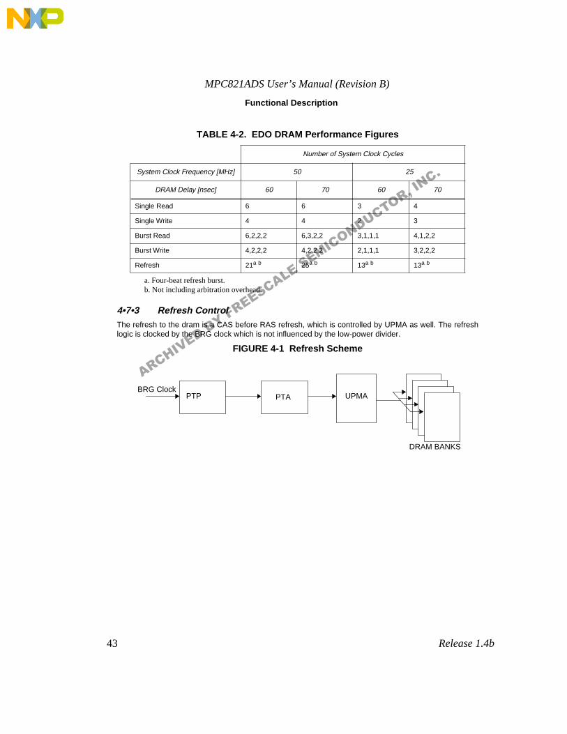
MPC821ADS User’s Manual (Revision B)
43 Release 1.4b
Functional Description
4•7•3 Refresh ControlThe refresh to the dram is a CAS before RAS refresh, which is controlled by UPMA as well. The refreshlogic is clocked by the BRG clock which is not influenced by the low-power divider.
FIGURE 4-1 Refresh Scheme
a. Four-beat refresh burst.b. Not including arbitration overhead.
TABLE 4-2. EDO DRAM Performance Figures
Number of System Clock Cycles
System Clock Frequency [MHz] 50 25
DRAM Delay [nsec] 60 70 60 70
Single Read 6 6 3 4
Single Write 4 4 2 3
Burst Read 6,2,2,2 6,3,2,2 3,1,1,1 4,1,2,2
Burst Write 4,2,2,2 4,2,2,2 2,1,1,1 3,2,2,2
Refresh 21a b 25a b 13a b 13a b
PTP PTA UPMA
DRAM BANKS
BRG Clock
ARCHIVED BY FREESCALE SEMICONDUCTOR, INC.

MPC821ADS User’s Manual (Revision B)
44 Release 1.4b
Functional Description
As seen in FIGURE 4-1 "Refresh Scheme" above, the BRG clock is twice divided: once by the PTP (Pe-riodic Timer Prescaler) and again by another prescaler - the PTA, dedicated for each UPM. If there aremore than one dram banks, than refresh cycles are performed for consecutive banks, therefore, refreshshould be made faster. The formula for calculation of the PTA is given below:
Where:
• PTA - Periodic Timer A filed in MAMR. The value of the 2’nd divider.
• Refresh_Period is the time (usually in msec) required to refresh a dram bank
• Number_Of_Beats_Per_Refresh_Cycle: using the UPM looping capability, it is possible toperform more than one refresh cycle per refresh burst (in fact upto 16).
• Number_Of_Rows_To_Refresh: the number of rows in a dram bank
• T_BRG: the cycle time of the BRG clock
• MPTPR: the value of the periodic timer prescaler (2 to 64)
• Number_Of_Banks: number of dram banks to refresh.
If we take for example a MCM36200 SIMM which has the following data:
• Refresh_Period == 16 msec
• Number_Of_Beats_Per_Refresh_Cycle: on the ADS it is 4.
• Number_Of_Rows_To_Refresh == 1024
• T_BRG == 40 nsec (1/2 system clock @ 50 Mhz)
• MPTPR arbitrarily chosen to be 8
• Number_Of_Banks == 2 for that SIMM
If we assign the figures to the PTA formula we get the value of PTA should be 97 decimal or 61 hex.
The programming of the appropriate registers and UPM’s memory, controlling this function, is shown in3•4•1 "Memory Controller Registers Programming" on page 24.
4•7•4 Variable Bus-Width ControlSince a port’s width determines its address connections, i.e., the number of address lines required for byte-selection varies (1 for 16-bit port and 2 for 32-bit port) according to the port’s width, it is necessary tochange address connections to a memory port if its width is to be changed. E.g.: if a certain memory isinitially configured as a 32-bit port, the list significant address line which is connected to that memory’s A0line should be the MPC821’s ADD29. Now, if that port is to be reconfigured as a 16-bit port, the LS addressline becomes ADD30.
If a linearA address scheme is to be maintained, all address lines connected to that memory are to beshifted one bit, this obviously involves extensive multiplexing (passive or active). If linear addressingscheme is not a must, than only minimal multiplexing is required to support variable port width.
A. Consequent addresses lead to adjacent memory cells
PTA = Refresh_Period X Number_Of_Beats_Per_Refresh_Cycle
Number_Of_Rows_To_Refresh X X MPTPR X Number_Of_BanksT_BRG
ARCHIVED BY FREESCALE SEMICONDUCTOR, INC.
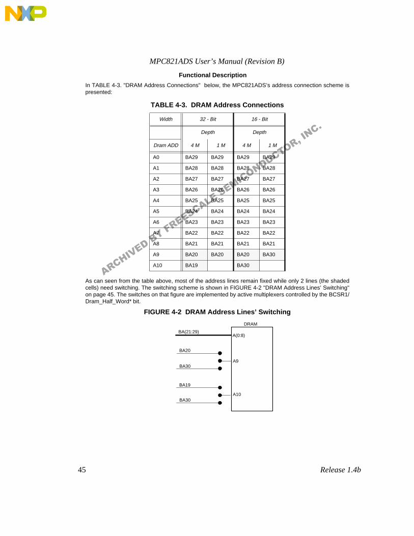
MPC821ADS User’s Manual (Revision B)
45 Release 1.4b
Functional Description
In TABLE 4-3. "DRAM Address Connections" below, the MPC821ADS’s address connection scheme ispresented:
As can seen from the table above, most of the address lines remain fixed while only 2 lines (the shadedcells) need switching. The switching scheme is shown in FIGURE 4-2 "DRAM Address Lines’ Switching"on page 45. The switches on that figure are implemented by active multiplexers controlled by the BCSR1/Dram_Half_Word* bit.
FIGURE 4-2 DRAM Address Lines’ Switching
TABLE 4-3. DRAM Address Connections
Width 32 - Bit 16 - Bit
Depth Depth
Dram ADD 4 M 1 M 4 M 1 M
A0 BA29 BA29 BA29 BA29
A1 BA28 BA28 BA28 BA28
A2 BA27 BA27 BA27 BA27
A3 BA26 BA26 BA26 BA26
A4 BA25 BA25 BA25 BA25
A5 BA24 BA24 BA24 BA24
A6 BA23 BA23 BA23 BA23
A7 BA22 BA22 BA22 BA22
A8 BA21 BA21 BA21 BA21
A9 BA20 BA20 BA20 BA30
A10 BA19 BA30
A(0:8)
A9
A10
BA(21:29)
BA20
BA30
BA19
BA30
DRAM
ARCHIVED BY FREESCALE SEMICONDUCTOR, INC.
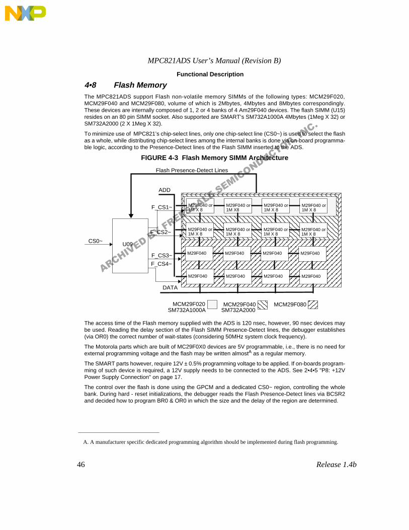
MPC821ADS User’s Manual (Revision B)
46 Release 1.4b
Functional Description
4•8 Flash MemoryThe MPC821ADS support Flash non-volatile memory SIMMs of the following types: MCM29F020,MCM29F040 and MCM29F080, volume of which is 2Mbytes, 4Mbytes and 8Mbytes correspondingly.These devices are internally composed of 1, 2 or 4 banks of 4 Am29F040 devices. The flash SIMM (U15)resides on an 80 pin SIMM socket. Also supported are SMART’s SM732A1000A 4Mbytes (1Meg X 32) orSM732A2000 (2 X 1Meg X 32).
To minimize use of MPC821’s chip-select lines, only one chip-select line (CS0~) is used to select the flashas a whole, while distributing chip-select lines among the internal banks is done via on-board programma-ble logic, according to the Presence-Detect lines of the Flash SIMM inserted to the ADS.
FIGURE 4-3 Flash Memory SIMM Architecture
The access time of the Flash memory supplied with the ADS is 120 nsec, however, 90 nsec devices maybe used. Reading the delay section of the Flash SIMM Presence-Detect lines, the debugger establishes(via OR0) the correct number of wait-states (considering 50MHz system clock frequency).
The Motorola parts which are built of MC29F0X0 devices are 5V programmable, i.e., there is no need forexternal programming voltage and the flash may be written almostA as a regular memory.
The SMART parts however, require 12V ± 0.5% programming voltage to be applied. If on-boards program-ming of such device is required, a 12V supply needs to be connected to the ADS. See 2•4•5 "P8: +12VPower Supply Connection" on page 17.
The control over the flash is done using the GPCM and a dedicated CS0~ region, controlling the wholebank. During hard - reset initializations, the debugger reads the Flash Presence-Detect lines via BCSR2and decided how to program BR0 & OR0 in which the size and the delay of the region are determined.
A. A manufacturer specific dedicated programming algorithm should be implemented during flash programming.
M29F040 or M29F040 or M29F040 or M29F040 or
M29F040 or M29F040 or M29F040 or M29F040 or
M29F040 M29F040 M29F040 M29F040
M29F040 M29F040 M29F040 M29F040
MCM29F020 MCM29F040 MCM29F080
ADD
DATA
F_CS1~
F_CS2~
F_CS3~
F_CS4~
Flash Presence-Detect Lines
CS0~ U09
1M X 8 1M X8 1M X 8 1M X 8
1M X 8 1M X 8 1M X 8 1M X 8
SM732A1000A SM732A2000
ARCHIVED BY FREESCALE SEMICONDUCTOR, INC.

MPC821ADS User’s Manual (Revision B)
47 Release 1.4b
Functional Description
The performance of the flash memory is shown in TABLE 4-4. "Flash Memory Performance Figures"below:
The programming of the associated registers is shown in 3•4•1 "Memory Controller Registers Program-ming" on page 24.
The Flash module may disabled / enabled at any time by writing ’1’ / ’0’ the FlashEn~ bit in BCSR1.
4•9 Ethernet PortAn Ethernet port with T.P. (10-Base-T) I/F is provided on the MPC821ADS. This port resides over SCC1ofthe MPC821. Use is done with Motorola’s MC68160 EEST (Enhanced Ethernet Serial Transceiver) tomediate between the SCC and the Ethernet medium.
To allow external use of SCC1, its pins appear at the expansion connectors and the ethernet transceivermay be Disabled / Enabled at any time by writing ’1’ / ’0’ to the EthEn~ bit in BCSR1.
The EEST is configured constantly to Twisted Pair I/F with automatic polarity correction enabled.
There are few control lines which control the EEST function and are driven by MPC821’s parallel I/O lines:
1) TPSQEL~ - Twisted Pair Signal Quality Error Test Enable. This active-low signal enables testing of the internal TP collision detect circuitry after each transmit to the TP media. It is connected to PC6A of the MPC821 and should be driven to ’1’ during normal operation.
2) TPFLDL~ - Twisted Pair Full Duplex Mode Select. This active low signal allows simultaneous transmit and receive over the twisted pair lines without indicated collision. This signal is connect-ed to PC5A of the MPC821 and should be driven to ’0’ during normal operation.
3) ETHLOOP - Diagnostic Loopback. This active high signal puts the EEST in diagnostic loopback mode, regardless of the I/F type it is configured to. This line is connected to PC4A of the MPC821 and should be driven to ’0’ during normal operation.
For additional information on the EEST refer to the "MC68160 Technical Data" document.
4•10 Infra - Red PortAn infra-red communication port is provided with the MPC821ADS - the Temic’s TFDS 3000 integratedtransceiver, which incorporates both the receiver and transmitter optical devices with the translating logic.This port resides on SCC2 of the MPC821. This device conforms to the IRDA standard, which is supportedby the MPC821 allowing for glueless connection between the TFDS3000 and the MPC821.
To allow SCC2’s off-board use, the infra-red transceiver may be disabled / enabled at any time, by writing’1’ / ’0’ to the IrdEn~ bit in BCSR1.
a. The figures in the table refer to the actual write access. The write operation continues internallyand the device has to be polled for completion.
A. After Hard reset this line wakes-up as Tri-state. For proper operation it should be initialized as Output.
TABLE 4-4. Flash Memory Performance Figures
Number of System Clock Cycles
System Clock Frequency [MHz] 50 25
Flash Delay [nsec] 90 120 90 120
Read / Writea Access [Clocks] 8 10 4 5
ARCHIVED BY FREESCALE SEMICONDUCTOR, INC.
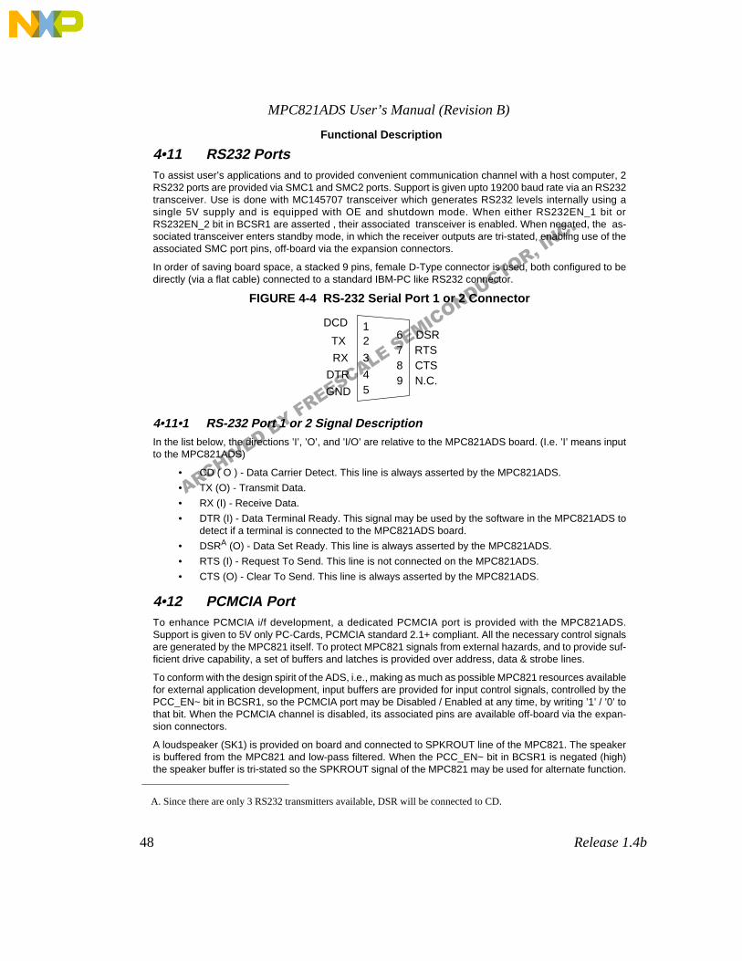
MPC821ADS User’s Manual (Revision B)
48 Release 1.4b
Functional Description
4•11 RS232 PortsTo assist user’s applications and to provided convenient communication channel with a host computer, 2RS232 ports are provided via SMC1 and SMC2 ports. Support is given upto 19200 baud rate via an RS232transceiver. Use is done with MC145707 transceiver which generates RS232 levels internally using asingle 5V supply and is equipped with OE and shutdown mode. When either RS232EN_1 bit orRS232EN_2 bit in BCSR1 are asserted , their associated transceiver is enabled. When negated, the as-sociated transceiver enters standby mode, in which the receiver outputs are tri-stated, enabling use of theassociated SMC port pins, off-board via the expansion connectors.
In order of saving board space, a stacked 9 pins, female D-Type connector is used, both configured to bedirectly (via a flat cable) connected to a standard IBM-PC like RS232 connector.
FIGURE 4-4 RS-232 Serial Port 1 or 2 Connector
4•11•1 RS-232 Port 1 or 2 Signal Description In the list below, the directions ’I’, ’O’, and ’I/O’ are relative to the MPC821ADS board. (I.e. ’I’ means inputto the MPC821ADS)
• CD ( O ) - Data Carrier Detect. This line is always asserted by the MPC821ADS.
• TX (O) - Transmit Data.
• RX (I) - Receive Data.
• DTR (I) - Data Terminal Ready. This signal may be used by the software in the MPC821ADS todetect if a terminal is connected to the MPC821ADS board.
• DSRA (O) - Data Set Ready. This line is always asserted by the MPC821ADS.
• RTS (I) - Request To Send. This line is not connected on the MPC821ADS.
• CTS (O) - Clear To Send. This line is always asserted by the MPC821ADS.
4•12 PCMCIA PortTo enhance PCMCIA i/f development, a dedicated PCMCIA port is provided with the MPC821ADS.Support is given to 5V only PC-Cards, PCMCIA standard 2.1+ compliant. All the necessary control signalsare generated by the MPC821 itself. To protect MPC821 signals from external hazards, and to provide suf-ficient drive capability, a set of buffers and latches is provided over address, data & strobe lines.
To conform with the design spirit of the ADS, i.e., making as much as possible MPC821 resources availablefor external application development, input buffers are provided for input control signals, controlled by thePCC_EN~ bit in BCSR1, so the PCMCIA port may be Disabled / Enabled at any time, by writing ’1’ / ’0’ tothat bit. When the PCMCIA channel is disabled, its associated pins are available off-board via the expan-sion connectors.
A loudspeaker (SK1) is provided on board and connected to SPKROUT line of the MPC821. The speakeris buffered from the MPC821 and low-pass filtered. When the PCC_EN~ bit in BCSR1 is negated (high)the speaker buffer is tri-stated so the SPKROUT signal of the MPC821 may be used for alternate function.
A. Since there are only 3 RS232 transmitters available, DSR will be connected to CD.
1
RX
2TX
3RTS
4CTS
5
DSR6
GND
7
DCD
89 N.C.DTR
ARCHIVED BY FREESCALE SEMICONDUCTOR, INC.
MPC821ADS User’s Manual (Revision B)
49 Release 1.4b
Functional Description
4•12•1 PCMCIA Power ControlTo support hot-insertionA the socket’s power is controlled via a dedicated PCMCIA power controller theLTC1315 made by LINEAR TECHNOLOGY. This device, controlled by BCSR1, switches 12V VPP for cardprogramming and controls gates of external MOSFET transistors, through which the PC Card VCC isswitched.
When a card is inserted and the channel is enabled via BCSR1, i.e., both of the CD(1:2)* (Card Detect)lines are asserted (low), the status of the voltage select lines VS(1:2)* should be read to determine the PCCard’s operation voltage level and then if the PC-Card is found to be 5V operated, the BCSR1 may bewritten to turn on power (5V only) to the PC Card’s VCC. If a 3.3V card is inserted, power should never beswitched-on.
When a card is being removed from the socket while the channel is enabled via BCSR1, the negation ofCD1~ and CD2~ is sensed by the MPC821 and power supply to the card may be cut.
WARNINGAny application S/W handling the PCMCIA channel must check the Voltage-Sense lines before Power is applied to the PC-Card. Otherwise if power is applied to a 3.3V-Only card, permanent damage might be inflicted to the PC-Card.
The LTC1315 may control power and VPP for 2 PC-Cards. Since there is only one PCMCIA socket on theADS, the power control lines for the 2’nd socket are used for optional 3.3V supply to the DRAM simm.When the DRMPD5 signal is connected to GND, the DRAM is powered with 3.3V VCC.
4•13 LCD PortSince the I/F to the LCD is glueless, the only support given by the MPC821ADS for LCD display connectionis a dedicated 30 pin header connector, from which a flat cable may be drawn to any kind of screen avail-able. All LCD (Port D) pins appear also at P10 and P13 which are the communication connectors.
It is important to remember that the levels issued by the MPC821 over the LCD lines are between 0 - 3.3V.Some screens have 5V CMOS compatible inputs for which 3.3V level leaves very small noise margin. Forthis kind of screen it is advised to use CMOS buffers with TTL compatible inputs, so that the screen getsits appropriate levels.
A. I.e., card insertion when the MPC821ADS is powered
ARCHIVED BY FREESCALE SEMICONDUCTOR, INC.
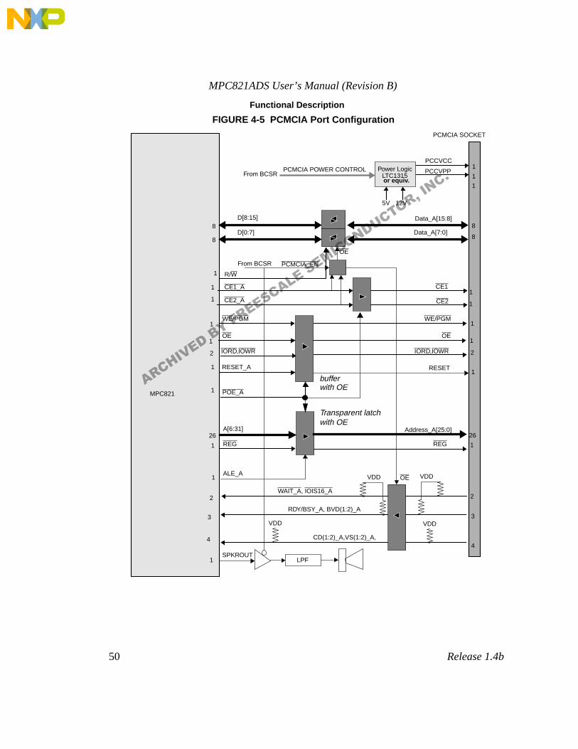
MPC821ADS User’s Manual (Revision B)
50 Release 1.4b
Functional Description
FIGURE 4-5 PCMCIA Port Configuration
5
D[8:15]
D[0:7]
CE2_A
CE1_A
ALE_A
Data_A[7:0]
Data_A[15:8]
R/W
RDY/BSY_A, BVD(1:2)_A
WE/PGM
Address_A[25:0]
CE1
CE2
12V
Power Logic
A[6:31]
8
8
1
1
26
1
1
1
PCCVCC
PCCVPP
5V
1
WE/PGM
REG 1REG
OE1
OE
IORD,IOWR 2IORD,IOWR
RESET_A
2
SPKROUT
1
1
26
3
1
1
1
2
2
8
8
1
1
3
1
or equiv.
WAIT_A, IOIS16_A
POE_A1
1
4
bufferwith OE
Transparent latch with OE
CD(1:2)_A,VS(1:2)_A,4
VDD
VDD
From BCSR
RESET1
VDD
VDD
PCMCIA_EN
MPC821
PCMCIA POWER CONTROL
PCMCIA SOCKET
OE
From BCSR
OE
LTC1315
LPF
ARCHIVED BY FREESCALE SEMICONDUCTOR, INC.

MPC821ADS User’s Manual (Revision B)
51 Release 1.4b
Functional Description
4•14 Board Control & Status Register - BCSRMost of the hardware options on the FADS are controlled or monitored by the BCSR, which is a 32A bitwide read / write register. The BCSR is accessed via the MPC821’s CS1 region and in fact includes 4 reg-isters: BCSR0 to BCSR3. Since the minimum block size for a CS region is 32KBytes, BCSR0 - BCSR3 aremultiply duplicated inside that region. See also 3•3 "MEMORY MAP" on page 23.
The following functions are controlled / monitored by the BCSR:
1) MPC821’s Hard Reset Configuration.
2) Flash Module Enable / Disable
3) Dram Module Enable / Disable
4) Dram port width - 32 bit / 16 bit.
5) Ethernet port Enable / Disable.
6) Infra-Red port Enable / Disable.
7) RS232 port 1 Enable / Disable.
8) RS232 port 2 Enable / Disable.
9) BCSR Enable / Disable.
10) Hard_Reset Configuration Source - BCSR0 / FlashB Memory
11) PCMCIA control which include:
• Channel Enable / Disable.
• PC Card VCC appliance.
• PC Card VPP appliance.
12) Dram Type / Size and Delay Identification.
13) Flash Size / Delay Identification.
14) External (off-board) tools identification or S/W option selection switch - DS2 status.
Since most of the MPC821ADS’s modules are controlled via the BCSR and since they may be disabled infavor of external hardware, the enable signals for these modules are presented at the expansion connec-tor, so that off- board hardware may be exclusive-or enabled with on-board modules.
4•14•1 BCSR Disable Protection LogicThe BCSR itself may be disabled in favor of off-board logic. To avoid accidental disable of the BCSR, anevent from which only power down recovers, a protection logic is provided:
The BCSR_EN~ bit resides on BCSR1. This bit wakes-up active (low) during power-up and may not bechangedC unless BCSR_EN_PROTECT~ bit in BCSR3 is written with ’1’ previously.
After the BCSR_EN_PROTECT~ is written with ’1’ to unprotect the BCSR_EN~ bit there is only one shotat disabling the BCSR, since, immediately after any write to BCSR1, BCSR_EN_PROTECT~ is re-activat-ed and BCSR_EN~ is re-protected and the disabling procedure has to be repeated if desired.
A. In fact only the upper 16 bits - D(0:15) are used, but the BCSR is mapped as a 32 bit wide register and should beaccessed as such.
B. Provided that support is provided also within the MPC821.C. It may be written but will not be influenced.
ARCHIVED BY FREESCALE SEMICONDUCTOR, INC.
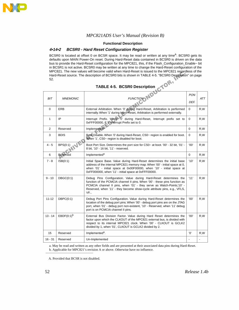
MPC821ADS User’s Manual (Revision B)
52 Release 1.4b
Functional Description
4•14•2 BCSR0 - Hard Reset Configuration RegisterBCSR0 is located at offset 0 on BCSR space. It may be read or written at any timeA. BCSR0 gets itsdefaults upon MAIN Power-On reset. During Hard-Reset data contained in BCSR0 is driven on the databus to provide the Hard-Reset configuration for the MPC821, this, if the Flash_Configuration_Enable~ bitin BCSR1 is not active. BCSR0 may be written at any time to change the Hard-Reset configuration of theMPC821. The new values will become valid when Hard-Reset is issued to the MPC821 regardless of theHard-Reset source. The description of BCSR0 bits is shown in TABLE 4-5. "BCSR0 Description" on page52.
A. Provided that BCSR is not disabled.
a. May be read and written as any other fields and are presented at their associated data pins during Hard-Reset.b. Applicable for MPC821’s revision A or above. Otherwise have no influence.
TABLE 4-5. BCSR0 Description
BIT MNEMONIC FUNCTIONPON
DEF.
ATT
0 ERB External Arbitration. When ’0’ during Hard-Reset, Arbitration is performedinternally. When ’1’ during Hard-Reset, Arbitration is performed externally.
0 R,W
1 IP Interrupt Prefix. When ’0’ during Hard-Reset, Interrupt prefix set to0xFFF00000, if ’1’ Interrupt Prefix set to 0.
0 R,W
2 Reserved Implementeda 0 R,W
3 BDIS Boot Disable. When ’0’ during Hard-Reset, CS0~ region is enabled for boot.When ’1’, CS0~ region is disabled for boot.
0 R,W
4 - 5 BPS(0:1) Boot Port Size. Determines the port size for CS0~ at boot. ’00’ - 32 bit, ’01’ -8 bit, ’10’ - 16 bit, ’11’ - reserved.
’00’ R,W
6 Reserved Implementeda 0 R,W
7 - 8 ISB(0:1) Initial Space Base. Value during Hard-Reset determines the initial baseaddress of the internal MPC821 memory map. When ’00’ - initial space at 0,when ’01’ - initial space at 0x00F00000, when ’10’ - initial space at0xFF000000, when ’11’ - initial space at 0xFFF00000.
’10’ R,W
9 - 10 DBGC(0:1) Debug Pins Configuration. Value during Hard-Reset determines thefunction of the PCMCIA channel II pins. When ’00’ - these pins function asPCMCIA channel II pins, when ’01’ - they serve as Watch-Points,’10’ -Reserved, when ’11’ - they become show-cycle attribute pins, e.g., VFLS,VF...
’11’ R,W
11-12 DBPC(0:1) Debug Port Pins Configuration. Value during Hard-Reset determines thelocation of the debug port pins. When ’00’ - debug port pins are on the JTAGport, when ’01’ - debug port non-existent, ’10’ - Reserved, when ’11’ debugport is on PCMCIA channel II pins.
’00’ R,W
13 - 14 EBDF(0:1)b External Bus Division Factor. Value during Hard Reset determines thefactor upon which the CLKOUT of the MPC821 external bus, is divided withrespect to its internal MPC821 clock. When ’00’ - CLKOUT is GCLK2divided by 1, when ’01’, CLKOUT is GCLK2 divided by 2.
’00’ R,W
15 Reserved Implementeda. ’0’ R,W
16 - 31 Reserved Un-Implemented - -
ARCHIVED BY FREESCALE SEMICONDUCTOR, INC.
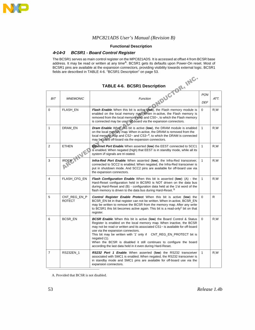
MPC821ADS User’s Manual (Revision B)
53 Release 1.4b
Functional Description
4•14•3 BCSR1 - Board Control RegisterThe BCSR1 serves as main control register on the MPC821ADS. It is accessed at offset 4 from BCSR baseaddress. It may be read or written at any timeA. BCSR1 gets its defaults upon Power-On reset. Most ofBCSR1 pins are available at the expansion connectors, providing visibility towards external logic. BCSR1fields are described in TABLE 4-6. "BCSR1 Description" on page 53.
A. Provided that BCSR is not disabled.
TABLE 4-6. BCSR1 Description
BIT MNEMONIC FunctionPON
DEF
ATT.
0 FLASH_EN Flash Enable . When this bit is active (low ), the Flash memory module isenabled on the local memory map. When in-active, the Flash memory isremoved from the local memory map and CS0~, to which the Flash memoryis connected may be used off-board via the expansion connectors.
0 R,W
1 DRAM_EN Dram Enable . When this bit is active (low ), the DRAM module is enabledon the local memory map. When in-active, the DRAM is removed from the local memory map and CS2~ and CS3~a, to which the DRAM is connectedmay be used off-board via the expansion connectors.
1 R,W
2 ETHEN Ethernet Port Enable . When asserted (low ) the EEST connected to SCC1is enabled. When negated (high) that EEST is in standby mode, while all itssystem i/f signals are tri-stated.
1 R,W
3 IRDEN Infra-Red Port Enable . When asserted (low ), the Infra-Red transceiver,connected to SCC2 is enabled. When negated, the Infra-Red transceiver isput in shutdown mode. And SCC2 pins are available for off-board use viathe expansion connectors.
1 R,W
4 FLASH_CFG_EN Flash Configuration Enable . When this bit is asserted (low ): (A) - theHard-Reset configuration held in BCSR0 is NOT driven on the data busduring Hard-Reset and (B) - configuration data held at the 1’st word of theflash memory is driven to the data bus during Hard-Reset. b
1 R,W
5 CNT_REG_EN_PROTECT
Control Register Enable Protect . When this bit is active (low ) theBCSR_EN bit in that register can not be written. When in-active, BCSR_ENmay be written to remove the BCSR from the memory map. After any writeto BCSR1 this bit becomes active again. This bit is a read-onlyc bit on thatregister.
0 R
6 BCSR_EN BCSR Enable . When this bit is active (low ) the Board Control & StatusRegister is enabled on the local memory map. When inactive, the BCSRmay not be read or written and its associated CS1~ is available for off-boarduse via the expansion connectors. This bit may be written with ’1’ only if CNT_REG_EN_PROTECT bit isnegated (1).When the BCSR is disabled it still continues to configure the boardaccording the last data held in it even during Hard-Reset.
0 R,W
7 RS232EN_1 RS232 Port 1 Enable . When asserted (low ) the RS232 transceiverassociated with SMC1 is enabled. When negated, the RS232 transceiver isin standby mode and SMC1 pins are available for off-board use via theexpansion connectors.
1 R,W
ARCHIVED BY FREESCALE SEMICONDUCTOR, INC.
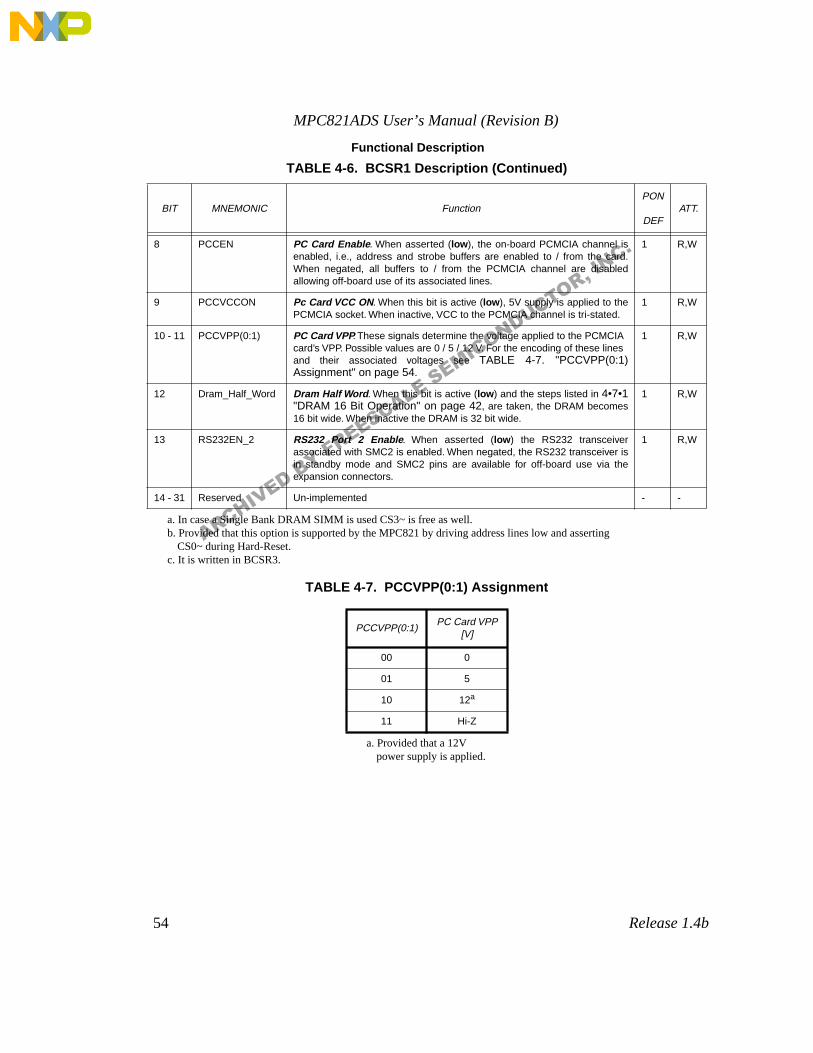
MPC821ADS User’s Manual (Revision B)
54 Release 1.4b
Functional Description
TABLE 4-7. PCCVPP(0:1) Assignment
a. In case a Single Bank DRAM SIMM is used CS3~ is free as well.b. Provided that this option is supported by the MPC821 by driving address lines low and asserting
CS0~ during Hard-Reset.c. It is written in BCSR3.
a. Provided that a 12V power supply is applied.
8 PCCEN PC Card Enable . When asserted (low ), the on-board PCMCIA channel isenabled, i.e., address and strobe buffers are enabled to / from the card.When negated, all buffers to / from the PCMCIA channel are disabledallowing off-board use of its associated lines.
1 R,W
9 PCCVCCON Pc Card VCC ON . When this bit is active (low ), 5V supply is applied to thePCMCIA socket. When inactive, VCC to the PCMCIA channel is tri-stated.
1 R,W
10 - 11 PCCVPP(0:1) PC Card VPP. These signals determine the voltage applied to the PCMCIA card’s VPP. Possible values are 0 / 5 / 12 V. For the encoding of these lines and their associated voltages see TABLE 4-7. "PCCVPP(0:1)Assignment" on page 54.
1 R,W
12 Dram_Half_Word Dram Half Word . When this bit is active (low ) and the steps listed in 4•7•1"DRAM 16 Bit Operation" on page 42, are taken, the DRAM becomes16 bit wide. When inactive the DRAM is 32 bit wide.
1 R,W
13 RS232EN_2 RS232 Port 2 Enable . When asserted (low ) the RS232 transceiverassociated with SMC2 is enabled. When negated, the RS232 transceiver isin standby mode and SMC2 pins are available for off-board use via theexpansion connectors.
1 R,W
14 - 31 Reserved Un-implemented - -
PCCVPP(0:1)PC Card VPP
[V]
00 0
01 5
10 12a
11 Hi-Z
TABLE 4-6. BCSR1 Description (Continued)
BIT MNEMONIC FunctionPON
DEF
ATT.
ARCHIVED BY FREESCALE SEMICONDUCTOR, INC.
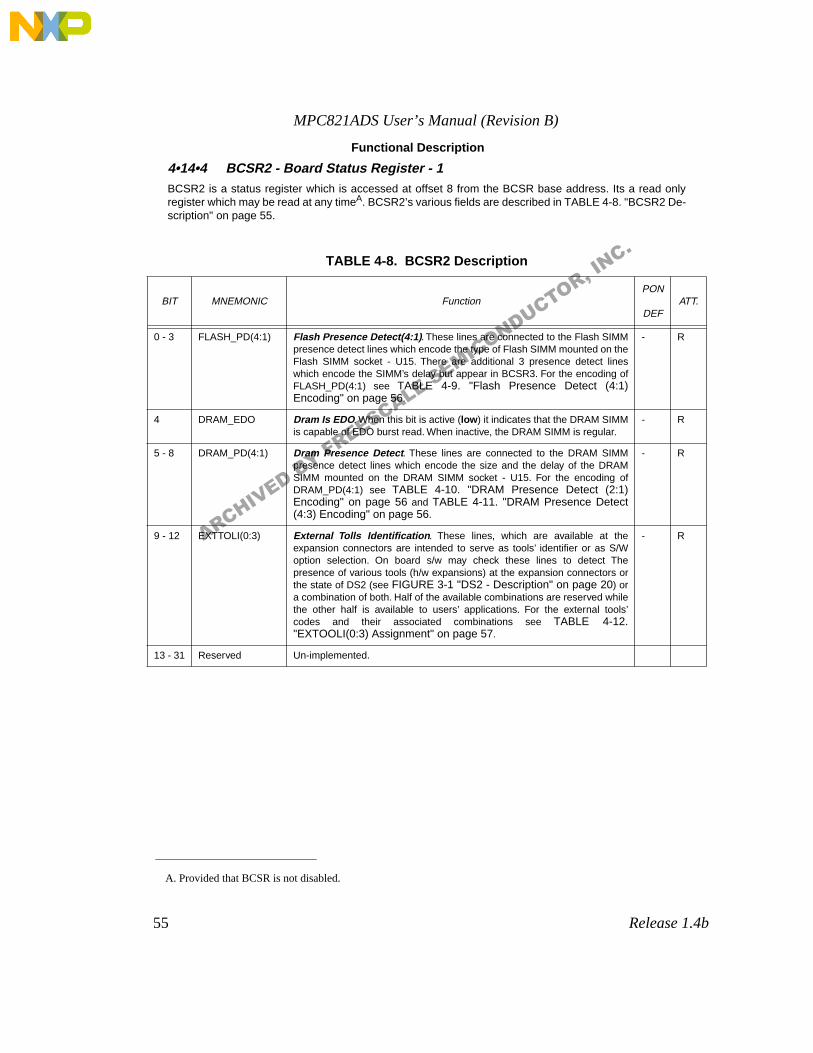
MPC821ADS User’s Manual (Revision B)
55 Release 1.4b
Functional Description
4•14•4 BCSR2 - Board Status Register - 1BCSR2 is a status register which is accessed at offset 8 from the BCSR base address. Its a read onlyregister which may be read at any timeA. BCSR2’s various fields are described in TABLE 4-8. "BCSR2 De-scription" on page 55.
A. Provided that BCSR is not disabled.
TABLE 4-8. BCSR2 Description
BIT MNEMONIC FunctionPON
DEF
ATT.
0 - 3 FLASH_PD(4:1) Flash Presence Detect(4:1) . These lines are connected to the Flash SIMMpresence detect lines which encode the type of Flash SIMM mounted on theFlash SIMM socket - U15. There are additional 3 presence detect lineswhich encode the SIMM’s delay but appear in BCSR3. For the encoding ofFLASH_PD(4:1) see TABLE 4-9. "Flash Presence Detect (4:1)Encoding" on page 56.
- R
4 DRAM_EDO Dram Is EDO . When this bit is active (low ) it indicates that the DRAM SIMMis capable of EDO burst read. When inactive, the DRAM SIMM is regular.
- R
5 - 8 DRAM_PD(4:1) Dram Presence Detect . These lines are connected to the DRAM SIMMpresence detect lines which encode the size and the delay of the DRAMSIMM mounted on the DRAM SIMM socket - U15. For the encoding ofDRAM_PD(4:1) see TABLE 4-10. "DRAM Presence Detect (2:1)Encoding" on page 56 and TABLE 4-11. "DRAM Presence Detect(4:3) Encoding" on page 56.
- R
9 - 12 EXTTOLI(0:3) External Tolls Identification . These lines, which are available at theexpansion connectors are intended to serve as tools’ identifier or as S/Woption selection. On board s/w may check these lines to detect Thepresence of various tools (h/w expansions) at the expansion connectors orthe state of DS2 (see FIGURE 3-1 "DS2 - Description" on page 20) ora combination of both. Half of the available combinations are reserved whilethe other half is available to users’ applications. For the external tools’codes and their associated combinations see TABLE 4-12."EXTOOLI(0:3) Assignment" on page 57.
- R
13 - 31 Reserved Un-implemented.
ARCHIVED BY FREESCALE SEMICONDUCTOR, INC.
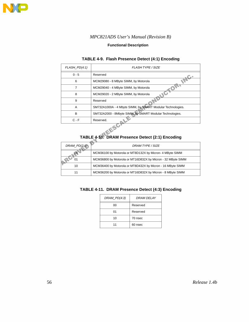
MPC821ADS User’s Manual (Revision B)
56 Release 1.4b
Functional Description
TABLE 4-9. Flash Presence Detect (4:1) Encoding
FLASH_PD(4:1) FLASH TYPE / SIZE
0 - 5 Reserved
6 MCM29080 - 8 MByte SIMM, by Motorola
7 MCM29040 - 4 MByte SIMM, by Motorola
8 MCM29020 - 2 MByte SIMM, by Motorola
9 Reserved
A SM732A1000A - 4 Mbyte SIMM, by SMART Modular Technologies.
B SM732A2000 - 8Mbyte SIMM, by SMART Modular Technologies.
C - F Reserved.
TABLE 4-10. DRAM Presence Detect (2:1) Encoding
DRAM_PD(2:1) DRAM TYPE / SIZE
00 MCM36100 by Motorola or MT8D132X by Micron- 4 MByte SIMM
01 MCM36800 by Motorola or MT16D832X by Micron - 32 MByte SIMM
10 MCM36400 by Motorola or MT8D432X by Micron - 16 MByte SIMM
11 MCM36200 by Motorola or MT16D832X by Micron - 8 MByte SIMM
TABLE 4-11. DRAM Presence Detect (4:3) Encoding
DRAM_PD(4:3) DRAM DELAY
00 Reserved
01 Reserved
10 70 nsec
11 60 nsec
ARCHIVED BY FREESCALE SEMICONDUCTOR, INC.
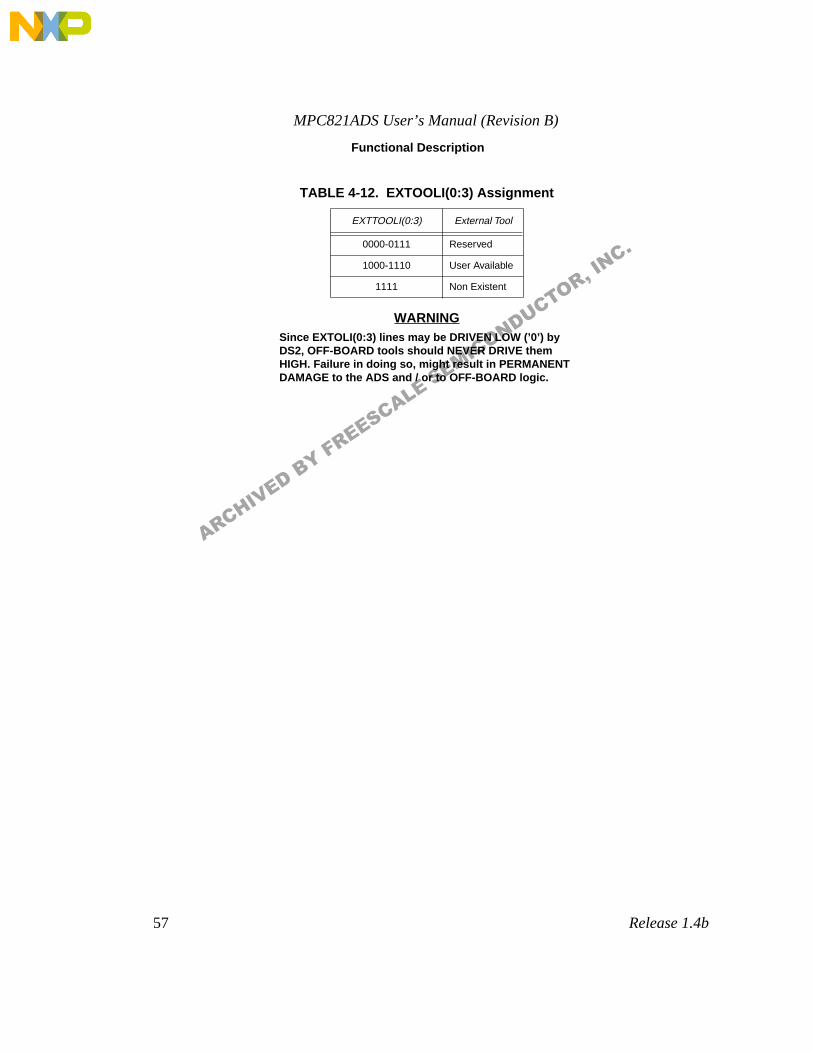
MPC821ADS User’s Manual (Revision B)
57 Release 1.4b
Functional Description
WARNINGSince EXTOLI(0:3) lines may be DRIVEN LOW (’0’) by DS2, OFF-BOARD tools should NEVER DRIVE them HIGH. Failure in doing so, might result in PERMANENT DAMAGE to the ADS and / or to OFF-BOARD logic.
TABLE 4-12. EXTOOLI(0:3) Assignment
EXTTOOLI(0:3) External Tool
0000-0111 Reserved
1000-1110 User Available
1111 Non Existent
ARCHIVED BY FREESCALE SEMICONDUCTOR, INC.
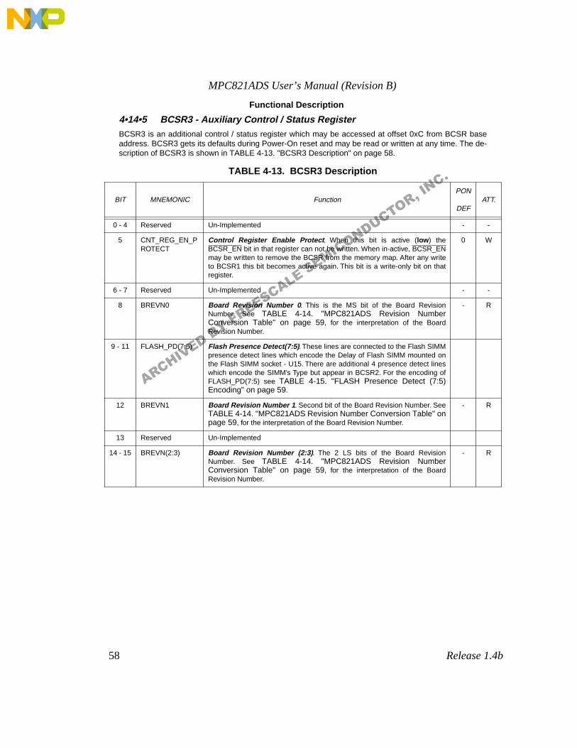
MPC821ADS User’s Manual (Revision B)
58 Release 1.4b
Functional Description
4•14•5 BCSR3 - Auxiliary Control / Status RegisterBCSR3 is an additional control / status register which may be accessed at offset 0xC from BCSR baseaddress. BCSR3 gets its defaults during Power-On reset and may be read or written at any time. The de-scription of BCSR3 is shown in TABLE 4-13. "BCSR3 Description" on page 58.
TABLE 4-13. BCSR3 Description
BIT MNEMONIC FunctionPON
DEF
ATT.
0 - 4 Reserved Un-Implemented - -
5 CNT_REG_EN_PROTECT
Control Register Enable Protect . When this bit is active (low ) theBCSR_EN bit in that register can not be written. When in-active, BCSR_ENmay be written to remove the BCSR from the memory map. After any writeto BCSR1 this bit becomes active again. This bit is a write-only bit on thatregister.
0 W
6 - 7 Reserved Un-Implemented - -
8 BREVN0 Board Revision Number 0 . This is the MS bit of the Board RevisionNumber. See TABLE 4-14. "MPC821ADS Revision NumberConversion Table" on page 59, for the interpretation of the BoardRevision Number.
- R
9 - 11 FLASH_PD(7:5) Flash Presence Detect(7:5) . These lines are connected to the Flash SIMMpresence detect lines which encode the Delay of Flash SIMM mounted onthe Flash SIMM socket - U15. There are additional 4 presence detect lineswhich encode the SIMM’s Type but appear in BCSR2. For the encoding ofFLASH_PD(7:5) see TABLE 4-15. "FLASH Presence Detect (7:5)Encoding" on page 59.
12 BREVN1 Board Revision Number 1 . Second bit of the Board Revision Number. SeeTABLE 4-14. "MPC821ADS Revision Number Conversion Table" onpage 59, for the interpretation of the Board Revision Number.
- R
13 Reserved Un-Implemented
14 - 15 BREVN(2:3) Board Revision Number (2:3) . The 2 LS bits of the Board RevisionNumber. See TABLE 4-14. "MPC821ADS Revision NumberConversion Table" on page 59, for the interpretation of the BoardRevision Number.
- R
ARCHIVED BY FREESCALE SEMICONDUCTOR, INC.
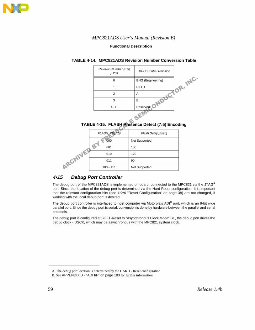
MPC821ADS User’s Manual (Revision B)
59 Release 1.4b
Functional Description
4•15 Debug Port ControllerThe debug port of the MPC821ADS is implemented on-board, connected to the MPC821 via the JTAGA
port. Since the location of the debug port is determined via the Hard-Reset configuration, It is importantthat the relevant configuration bits (see 4•2•6 "Reset Configuration" on page 38) are not changed, ifworking with the local debug port is desired.
The debug port controller is interfaced to host computer via Motorola’s ADIB port, which is an 8-bit wideparallel port. Since the debug port is serial, conversion is done by hardware between the parallel and serialprotocols.
The debug port is configured at SOFT-Reset to "Asynchronous Clock Mode" i.e., the debug port drives thedebug clock - DSCK, which may be asynchronous with the MPC821 system clock.
A. The debug port location is determined by the HARD - Reset configuration.B. See APPENDIX B - "ADI I/F" on page 183 for further information.
TABLE 4-14. MPC821ADS Revision Number Conversion Table
Revision Number (0:3) [Hex]
MPC821ADS Revision
0 ENG (Engineering)
1 PILOT
2 A
3 B
4 - F Reserved
TABLE 4-15. FLASH Presence Detect (7:5) Encoding
FLASH_PD(7:5) Flash Delay [nsec]
000 Not Supported
001 150
010 120
011 90
100 - 111 Not SupportedARCHIVED BY FREESCALE SEMICONDUCTOR, INC.
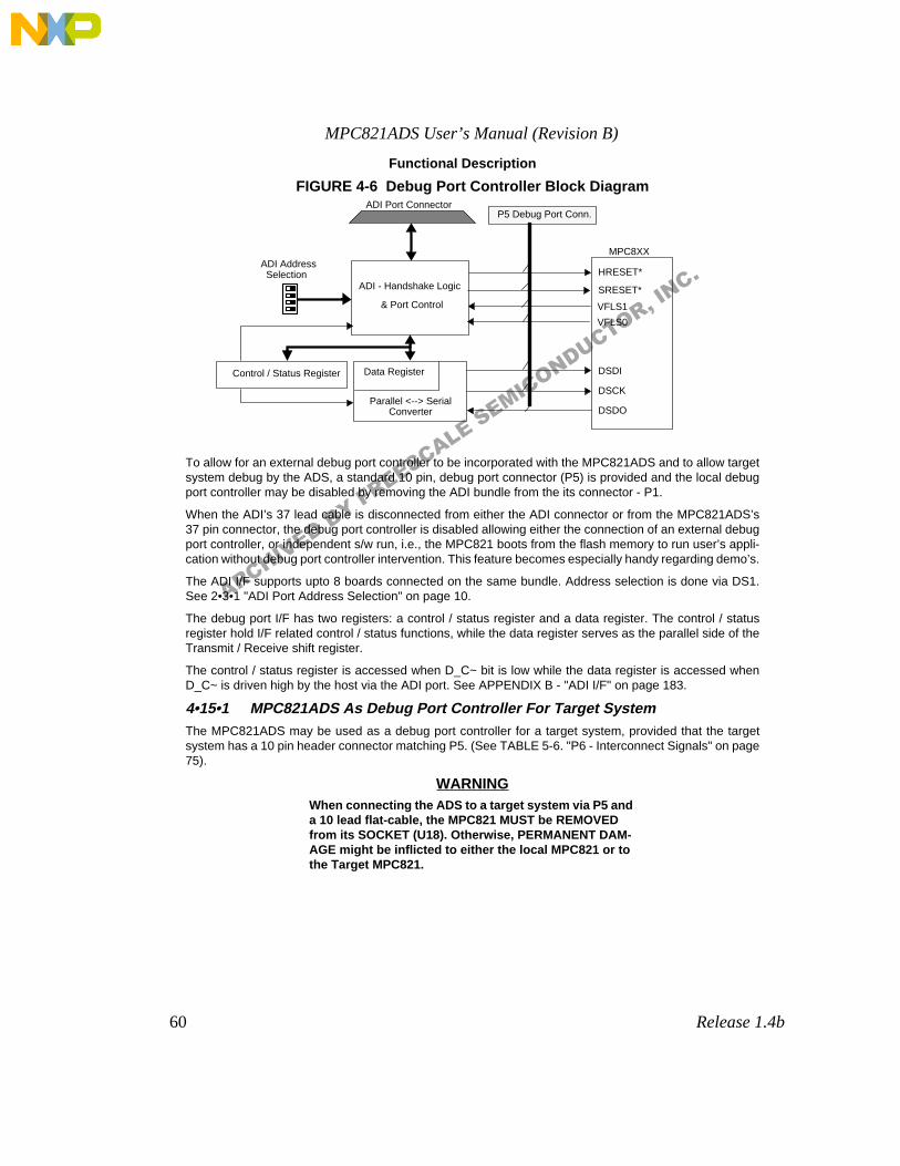
MPC821ADS User’s Manual (Revision B)
60 Release 1.4b
Functional Description
FIGURE 4-6 Debug Port Controller Block Diagram
To allow for an external debug port controller to be incorporated with the MPC821ADS and to allow targetsystem debug by the ADS, a standard 10 pin, debug port connector (P5) is provided and the local debugport controller may be disabled by removing the ADI bundle from the its connector - P1.
When the ADI’s 37 lead cable is disconnected from either the ADI connector or from the MPC821ADS’s37 pin connector, the debug port controller is disabled allowing either the connection of an external debugport controller, or independent s/w run, i.e., the MPC821 boots from the flash memory to run user’s appli-cation without debug port controller intervention. This feature becomes especially handy regarding demo’s.
The ADI I/F supports upto 8 boards connected on the same bundle. Address selection is done via DS1.See 2•3•1 "ADI Port Address Selection" on page 10.
The debug port I/F has two registers: a control / status register and a data register. The control / statusregister hold I/F related control / status functions, while the data register serves as the parallel side of theTransmit / Receive shift register.
The control / status register is accessed when D_C~ bit is low while the data register is accessed whenD_C~ is driven high by the host via the ADI port. See APPENDIX B - "ADI I/F" on page 183.
4•15•1 MPC821ADS As Debug Port Controller For Target SystemThe MPC821ADS may be used as a debug port controller for a target system, provided that the targetsystem has a 10 pin header connector matching P5. (See TABLE 5-6. "P6 - Interconnect Signals" on page75).
WARNINGWhen connecting the ADS to a target system via P5 and a 10 lead flat-cable, the MPC821 MUST be REMOVED from its SOCKET (U18). Otherwise, PERMANENT DAM-AGE might be inflicted to either the local MPC821 or to the Target MPC821.
ADI - Handshake Logic
DSDI
DSCK
DSDO
HRESET*
SRESET*
VFLS0
VFLS1& Port Control
Parallel <--> SerialConverter
ADI AddressSelection
MPC8XX
ADI Port Connector
Control / Status Register Data Register
P5 Debug Port Conn.
ARCHIVED BY FREESCALE SEMICONDUCTOR, INC.

MPC821ADS User’s Manual (Revision B)
61 Release 1.4b
Functional Description
In this mode of operation, the on-board debug port controller, is connected to the target system’s debug-port connector (see 4•15•1•1 "Debug Port Connection - Target System Requirements" below). SinceDSDO signal is driven by the MPC821, it is a must to remove the local MPC821 from its socket, to avoidcontention over this line.
When the local MPC821 is removed from its socket, all ADS’s modules are inaccessible, except for thedebug-port controller. All module-enable indications are darkened, regardless of their associated enablebits in the BCSR. Pull-up resistor are connected to Chip-Select lines, so they do not float when the MPC821is removed from its socket, avoiding possible contention over data-bus lines.
4•15•1•1 Debug Port Connection - Target System RequirementsIn order for a target system may be connected to the ADS, as a debug port controller, few measures needto be taken on the target system:
1) A 10-pin header connector should be made available, with electrical connections matching TA-BLE 5-6. "P6 - Interconnect Signals" on page 75.
2) Pull-down resistors, of app. 2KΩ should be connected over DSDIA and DSCKA signals. These resistors are to provide normalB operation, when a debug-port controller, is not connected to the target system
3) The debug-port should be enabled and routed to the desired pins. See the DBGC and DBPC fields within the HARD-RESET configuration word.
A. Remember that the location of DSDI and DSCK is determined by the HARD-Reset configuration.B. Normal - i.e., boot via CS0~.
ARCHIVED BY FREESCALE SEMICONDUCTOR, INC.
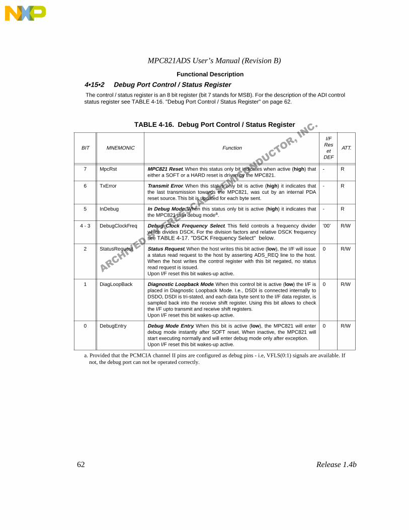
MPC821ADS User’s Manual (Revision B)
62 Release 1.4b
Functional Description
4•15•2 Debug Port Control / Status Register The control / status register is an 8 bit register (bit 7 stands for MSB). For the description of the ADI controlstatus register see TABLE 4-16. "Debug Port Control / Status Register" on page 62.
a. Provided that the PCMCIA channel II pins are configured as debug pins - i.e, VFLS(0:1) signals are available. Ifnot, the debug port can not be operated correctly.
TABLE 4-16. Debug Port Control / Status Register
BIT MNEMONIC Function
I/F Reset
DEF
ATT.
7 MpcRst MPC821 Reset. When this status only bit indicates when active (high ) thateither a SOFT or a HARD reset is driven by the MPC821.
- R
6 TxError Transmit Error . When this status only bit is active (high ) it indicates thatthe last transmission towards the MPC821, was cut by an internal PDAreset source. This bit is updated for each byte sent.
- R
5 InDebug In Debug Mode . When this status only bit is active (high ) it indicates thatthe MPC821 is in debug modea.
- R
4 - 3 DebugClockFreq Debug Clock Frequency Select . This field controls a frequency dividerwhich divides DSCK. For the division factors and relative DSCK frequencysee TABLE 4-17. "DSCK Frequency Select" below.
’00’ R/W
2 StatusRequest Status Request . When the host writes this bit active (low ), the I/F will issuea status read request to the host by asserting ADS_REQ line to the host.When the host writes the control register with this bit negated, no statusread request is issued.Upon I/F reset this bit wakes-up active.
0 R/W
1 DiagLoopBack Diagnostic Loopback Mode . When this control bit is active (low ) the I/F isplaced in Diagnostic Loopback Mode. I.e., DSDI is connected internally toDSDO, DSDI is tri-stated, and each data byte sent to the I/F data register, issampled back into the receive shift register. Using this bit allows to checkthe I/F upto transmit and receive shift registers.Upon I/F reset this bit wakes-up active.
0 R/W
0 DebugEntry Debug Mode Entry . When this bit is active (low ), the MPC821 will enterdebug mode instantly after SOFT reset. When inactive, the MPC821 willstart executing normally and will enter debug mode only after exception.Upon I/F reset this bit wakes-up active.
0 R/W
ARCHIVED BY FREESCALE SEMICONDUCTOR, INC.
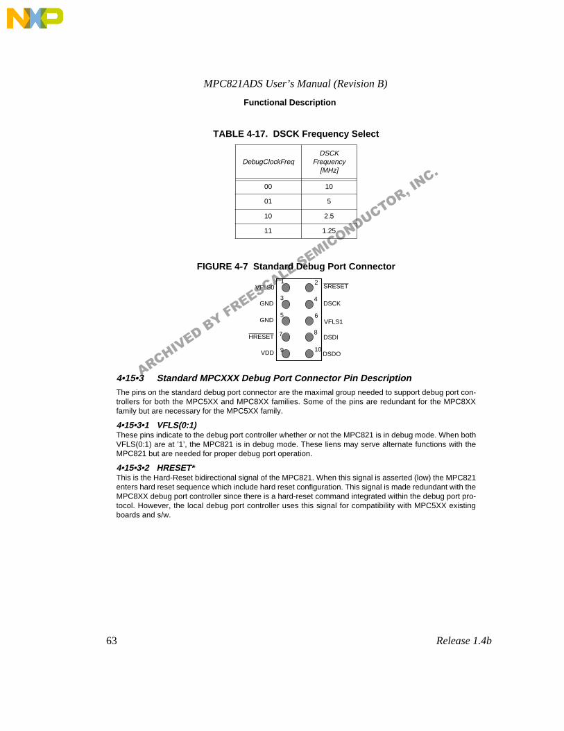
MPC821ADS User’s Manual (Revision B)
63 Release 1.4b
Functional Description
FIGURE 4-7 Standard Debug Port Connector
4•15•3 Standard MPCXXX Debug Port Connector Pin DescriptionThe pins on the standard debug port connector are the maximal group needed to support debug port con-trollers for both the MPC5XX and MPC8XX families. Some of the pins are redundant for the MPC8XXfamily but are necessary for the MPC5XX family.
4•15•3•1 VFLS(0:1) These pins indicate to the debug port controller whether or not the MPC821 is in debug mode. When bothVFLS(0:1) are at ’1’, the MPC821 is in debug mode. These liens may serve alternate functions with theMPC821 but are needed for proper debug port operation.
4•15•3•2 HRESET*This is the Hard-Reset bidirectional signal of the MPC821. When this signal is asserted (low) the MPC821enters hard reset sequence which include hard reset configuration. This signal is made redundant with theMPC8XX debug port controller since there is a hard-reset command integrated within the debug port pro-tocol. However, the local debug port controller uses this signal for compatibility with MPC5XX existingboards and s/w.
TABLE 4-17. DSCK Frequency Select
DebugClockFreqDSCK
Frequency [MHz]
00 10
01 5
10 2.5
11 1.25
1
3
5
7
9
2
4
6
8
10
VFLS0 SRESET
DSCK
VFLS1
DSDI
DSDO
GND
GND
HRESET
VDD
ARCHIVED BY FREESCALE SEMICONDUCTOR, INC.

MPC821ADS User’s Manual (Revision B)
64 Release 1.4b
Functional Description
4•15•3•3 SRESET* This is the Soft-Reset bidirectional signal of the MPC8XX. On the MPC5XX it is an output. The debug portconfiguration is sampled and determined on the rising-edgeA of SRESET* (for both processor families). Onthe MPC8XX it is a bidirectional signal which may be driven externally to generate soft reset sequence.This signal is in fact redundant regarding the MPC8XX debug port controller since there is a soft-resetcommand integrated within the debug port protocol. However, the local debug port controller uses thissignal for compatibility with MPC5XX existing boards and s/w.
4•15•3•4 DSDI - Debug-port Serial Data InVia the DSDI signal, the debug port controller sends its data to the MPC821. The DSDI serves also a roleduring soft-reset configuration. (See 4•2•6•3 "Soft Reset Configuration" on page 39).
4•15•3•5 DSCK - Debug-port Serial ClockDuring asynchronous clock mode, the serial data is clocked into the MPC821 accordingB to the DSCKclock. The DSCK serves also a role during soft-reset configuration. (See 4•2•6•3 "Soft Reset Configuration"on page 39).
4•15•3•6 DSDO - Debug-port Serial Data OutDSDO is clocked out by the MPC821 according to the debug port clock, in parallelC with the DSDI beingclocked in. The DSDO serves also as "READY" signal for the debug port controller to indicate that thedebug port is ready to receive controller’s command (or data).
4•16 PowerThere are 4 power buses with the MPC821:
1) I/O
2) Internal Logic
3) Keep Alive
4) PLL
and there are 4 power buses on the MPC821ADS:
1) 5V bus
2) 3.3V bus
3) 2.0V bus
4) 12V bus
A. In fact that configuration is divided into 2 parts, the first is sampled 3 system clock cycles prior to the rising edgeof SRESET* and the second is sampled 8 clocks after that edge.
B. I.e., DSDI must meat setup / hold time to / from rising edge of the DSCK.C. I.e., full-duplex communication.
ARCHIVED BY FREESCALE SEMICONDUCTOR, INC.
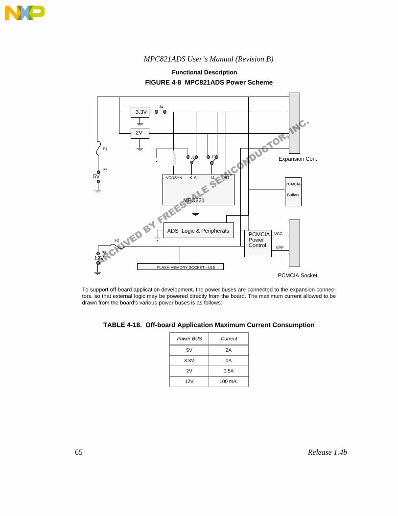
MPC821ADS User’s Manual (Revision B)
65 Release 1.4b
Functional Description
FIGURE 4-8 MPC821ADS Power Scheme
To support off-board application development, the power buses are connected to the expansion connec-tors, so that external logic may be powered directly from the board. The maximum current allowed to bedrawn from the board’s various power buses is as follows:
TABLE 4-18. Off-board Application Maximum Current Consumption
Power BUS Current
5V 2A
3.3V 0A
2V 0.5A
12V 100 mA.
3.3V
2V
5V
Expansion Con.
PCMCIA Socket
PCMCIAPowerControl
MPC821
I/O
12V
I.L.K.A.VDDSYN
VCC
VPP
PCMCIA
Buffers
ADS Logic & Peripherals
J4
J3 J2
F1
F2
P7
P8
FLASH MEMORY SOCKET - U15ARCHIVED BY FREESCALE SEMICONDUCTOR, IN
C.

MPC821ADS User’s Manual (Revision B)
66 Release 1.4b
Functional Description
To protect on board devices against supply spikes, decoupling capacitors (typically 0.1µF) are providedbetween the devices’ power leads and GND, located as close as possible to the power leads.
Special care is taken for PLL power leads, which has isolated "clean" ground and filtered VDD.
4•16•1 5V BusAll of the MPC821ADS peripherals reside on the 5V bus. Since the MPC821 is 5V friendly, it may operatewith 5V levels on its lines with no damage. The 5V bus is connected to an external power connector via afuse F1 of 5A fast-blow.
To protect against reverse-voltage or over-voltage being applied to the 5V inputs a set of high-currentdiodes and zener diode are connected between the 5V bus GND. When either over or reverse voltage isapplied to the MPC821ADS, the protection logic will blow the fuse, while limiting the momentary effects onboard.
4•16•2 3.3V BusThe MPC821 itself is powered by the 3.3A bus, which is produced from the 5V bus using a special low-voltage drop, linear voltage regulator made by Linear Technology, the LT1086 which is capable of drivingupto 1.5A. Since the local 3.3V current consumption might be around 1.5A, no power should be drawn fromthe 3.3V bus via the expansion connectors.
4•16•3 2V BusTo support evaluation of the MPC821 operating with two supply levels, i.e., internal logic is powered with2V and the I/O is powered with 3.3 - a dedicated 2V voltage regulator (LM317) is provided. That regulatoris also powered by the 5V bus.
The internal logic’s VDD may be switched between the 3.3V bus and the 2V bus, by means of a fabricatedjumper.
4•16•4 12V BusThe sole purpose of the 12V bus is to supply VPP (programming voltage) for the PCMCIA card and / or toa FLASH memory residing on U15. It is connected from a dedicated input connector - P8, via a fuse - F2(1A fast-blow) and protected from over / reverse voltage application by means of Zener diode and high-current diodes.
If the PCMCIA channel is not used or if a card which doesn’t require a 12V VPP is being used or the flashmemory available on-board does not require 12V for programming or both of them do not require program-ming, the 12V input to the MPC821ADS may be omitted.
4•16•5 Keep Alive PowerThe reason for the existence of the KAPWR bus is to allow current measurements over that bus and toallow the connection of an external power source to the KAPWR input of the MPC821. As seen in FIGURE4-8 "MPC821ADS Power Scheme" on page 65, it is possible to connect an external power source to theKAPWR rail. This can be done by removing the fabricated jumper from J3 and connected an external powersource between J3/2 and J3/3.
A. At full speed. When lower performance is needed the internal logic may be powered from the 2V bus.
ARCHIVED BY FREESCALE SEMICONDUCTOR, INC.

MPC821ADS User’s Manual (Revision B)
67
Release 1.4b
Support Information
5 - Support Information
In this chapter all information needed for support, maintenance and connectivity to the MPC821ADS is pro-vided.
5•1 Interconnect Signals
The MPC821ADS interconnects with external devices via the following set of connectors:
1) P1 - ADI Port connector
2) P2 - Ethernet port
3) PA3 - RS232 port 1
4) PB3 - RS232 port 2
5) P4 - PCMCIA port
6) P5 - External Debug port controller input
7) P6, P9, P10 & P12 - Expansion & Logic Analyzer connection
8) P7 - 5V Power In
9) P8 - 12V Power In
10) P11 - LCD port
11) P13 - Serial Expansion connector
ARCHIVED BY FREESCALE SEMICONDUCTOR, INC.
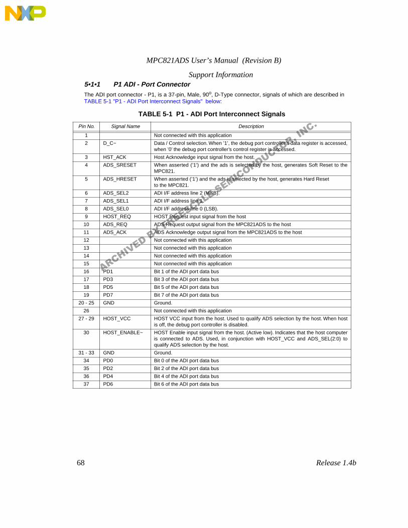
MPC821ADS User’s Manual (Revision B)
68
Release 1.4b
Support Information
5•1•1 P1 ADI - Port Connector
The ADI port connector - P1, is a 37-pin, Male, 90
o
, D-Type connector, signals of which are described inTABLE 5-1 "P1 - ADI Port Interconnect Signals" below:
TABLE 5-1 P1 - ADI Port Interconnect Signals
Pin No. Signal Name Description
1 Not connected with this application
2 D_C~ Data / Control selection. When ’1’, the debug port controller’s data register is accessed,when ’0’ the debug port controller’s control register is accessed.
3 HST_ACK Host Acknowledge input signal from the host.
4 ADS_SRESET When asserted (’1’) and the ads is selected by the host, generates Soft Reset to theMPC821.
5 ADS_HRESET When asserted (’1’) and the ads is selected by the host, generates Hard Reset to the MPC821.
6 ADS_SEL2 ADI I/F address line 2 (MSB).
7 ADS_SEL1 ADI I/F address line 1.
8 ADS_SEL0 ADI I/F address line 0 (LSB).
9 HOST_REQ HOST Request input signal from the host
10 ADS_REQ ADS Request output signal from the MPC821ADS to the host
11 ADS_ACK ADS Acknowledge output signal from the MPC821ADS to the host
12 Not connected with this application
13 Not connected with this application
14 Not connected with this application
15 Not connected with this application
16 PD1 Bit 1 of the ADI port data bus
17 PD3 Bit 3 of the ADI port data bus
18 PD5 Bit 5 of the ADI port data bus
19 PD7 Bit 7 of the ADI port data bus
20 - 25 GND Ground.
26 Not connected with this application
27 - 29 HOST_VCC HOST VCC input from the host. Used to qualify ADS selection by the host. When hostis off, the debug port controller is disabled.
30 HOST_ENABLE~ HOST Enable input signal from the host. (Active low). Indicates that the host computeris connected to ADS. Used, in conjunction with HOST_VCC and ADS_SEL(2:0) toqualify ADS selection by the host.
31 - 33 GND Ground.
34 PD0 Bit 0 of the ADI port data bus
35 PD2 Bit 2 of the ADI port data bus
36 PD4 Bit 4 of the ADI port data bus
37 PD6 Bit 6 of the ADI port data bus
ARCHIVED BY FREESCALE SEMICONDUCTOR, INC.
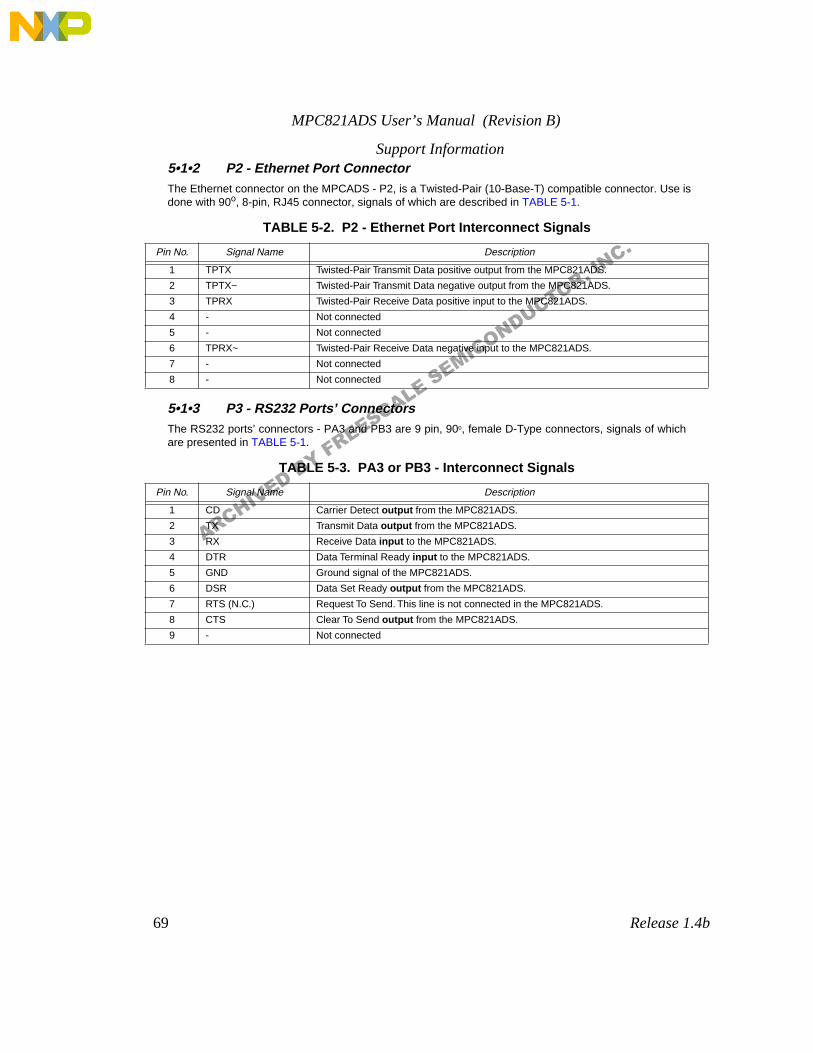
MPC821ADS User’s Manual (Revision B)
69
Release 1.4b
Support Information
5•1•2 P2 - Ethernet Port Connector
The Ethernet connector on the MPCADS - P2, is a Twisted-Pair (10-Base-T) compatible connector. Use is done with 90
o
, 8-pin, RJ45 connector, signals of which are described in TABLE 5-1.
5•1•3 P3 - RS232 Ports’ Connectors
The RS232 ports’ connectors - PA3 and PB3 are 9 pin, 90
o
, female D-Type connectors, signals of whichare presented in TABLE 5-1.
TABLE 5-2. P2 - Ethernet Port Interconnect Signals
Pin No. Signal Name Description
1 TPTX Twisted-Pair Transmit Data positive output from the MPC821ADS.
2 TPTX~ Twisted-Pair Transmit Data negative output from the MPC821ADS.
3 TPRX Twisted-Pair Receive Data positive input to the MPC821ADS.
4 - Not connected
5 - Not connected
6 TPRX~ Twisted-Pair Receive Data negative input to the MPC821ADS.
7 - Not connected
8 - Not connected
TABLE 5-3. PA3 or PB3 - Interconnect Signals
Pin No. Signal Name Description
1 CD Carrier Detect
output
from the MPC821ADS.
2 TX Transmit Data
output
from the MPC821ADS.
3 RX Receive Data
input
to the MPC821ADS.
4 DTR Data Terminal Ready
input
to the MPC821ADS.
5 GND Ground signal of the MPC821ADS.
6 DSR Data Set Ready
output
from the MPC821ADS.
7 RTS (N.C.) Request To Send. This line is not connected in the MPC821ADS.
8 CTS Clear To Send
output
from the MPC821ADS.
9 - Not connected
ARCHIVED BY FREESCALE SEMICONDUCTOR, INC.
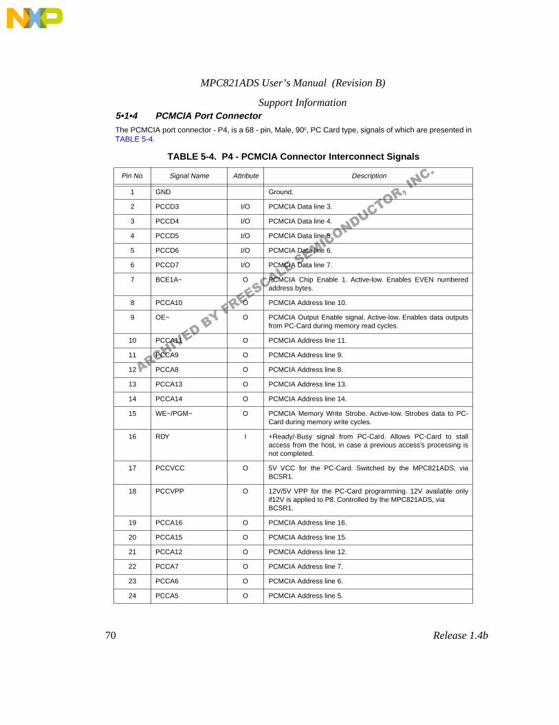
MPC821ADS User’s Manual (Revision B)
70
Release 1.4b
Support Information
5•1•4 PCMCIA Port Connector
The PCMCIA port connector - P4, is a 68 - pin, Male, 90
0
, PC Card type, signals of which are presented inTABLE 5-4.
TABLE 5-4. P4 - PCMCIA Connector Interconnect Signals
Pin No. Signal Name Attribute Description
1 GND Ground.
2 PCCD3 I/O PCMCIA Data line 3.
3 PCCD4 I/O PCMCIA Data line 4.
4 PCCD5 I/O PCMCIA Data line 5.
5 PCCD6 I/O PCMCIA Data line 6.
6 PCCD7 I/O PCMCIA Data line 7.
7 BCE1A~ O PCMCIA Chip Enable 1. Active-low. Enables EVEN numberedaddress bytes.
8 PCCA10 O PCMCIA Address line 10.
9 OE~ O PCMCIA Output Enable signal. Active-low. Enables data outputsfrom PC-Card during memory read cycles.
10 PCCA11 O PCMCIA Address line 11.
11 PCCA9 O PCMCIA Address line 9.
12 PCCA8 O PCMCIA Address line 8.
13 PCCA13 O PCMCIA Address line 13.
14 PCCA14 O PCMCIA Address line 14.
15 WE~/PGM~ O PCMCIA Memory Write Strobe. Active-low. Strobes data to PC-Card during memory write cycles.
16 RDY I +Ready/-Busy signal from PC-Card. Allows PC-Card to stallaccess from the host, in case a previous access’s processing isnot completed.
17 PCCVCC O 5V VCC for the PC-Card. Switched by the MPC821ADS, viaBCSR1.
18 PCCVPP O 12V/5V VPP for the PC-Card programming. 12V available onlyif12V is applied to P8. Controlled by the MPC821ADS, via BCSR1.
19 PCCA16 O PCMCIA Address line 16.
20 PCCA15 O PCMCIA Address line 15.
21 PCCA12 O PCMCIA Address line 12.
22 PCCA7 O PCMCIA Address line 7.
23 PCCA6 O PCMCIA Address line 6.
24 PCCA5 O PCMCIA Address line 5.
ARCHIVED BY FREESCALE SEMICONDUCTOR, INC.
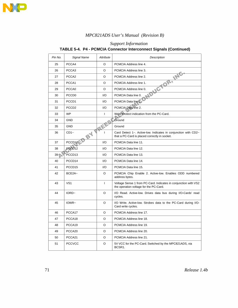
MPC821ADS User’s Manual (Revision B)
71
Release 1.4b
Support Information
25 PCCA4 O PCMCIA Address line 4.
26 PCCA3 O PCMCIA Address line 3.
27 PCCA2 O PCMCIA Address line 2.
28 PCCA1 O PCMCIA Address line 1.
29 PCCA0 O PCMCIA Address line 0.
30 PCCD0 I/O PCMCIA Data line 0.
31 PCCD1 I/O PCMCIA Data line 1.
32 PCCD2 I/O PCMCIA Data line 2.
33 WP I Write Protect indication from the PC-Card.
34 GND Ground
35 GND Ground
36 CD1~ I Card Detect 1~. Active-low. Indicates in conjunction with CD2~that a PC-Card is placed correctly in socket.
37 PCCD11 I/O PCMCIA Data line 11.
38 PCCD12 I/O PCMCIA Data line 12.
39 PCCD13 I/O PCMCIA Data line 13.
40 PCCD14 I/O PCMCIA Data line 14.
41 PCCD15 I/O PCMCIA Data line 15.
42 BCE2A~ O PCMCIA Chip Enable 2. Active-low. Enables ODD numberedaddress bytes.
43 VS1 I Voltage Sense 1 from PC-Card. Indicates in conjunction with VS2the operation voltage for the PC-Card.
44 IORD~ O I/O Read. Active-low. Drives data bus during I/O-Cards’ readcycles.
45 IOWR~ O I/O Write. Active-low. Strobes data to the PC-Card during I/O-Card write cycles.
46 PCCA17 O PCMCIA Address line 17.
47 PCCA18 O PCMCIA Address line 18.
48 PCCA19 O PCMCIA Address line 19.
49 PCCA20 O PCMCIA Address line 20.
50 PCCA21 O PCMCIA Address line 21.
51 PCCVCC O 5V VCC for the PC-Card. Switched by the MPC821ADS, via BCSR1.
TABLE 5-4. P4 - PCMCIA Connector Interconnect Signals (Continued)
Pin No. Signal Name Attribute Description
ARCHIVED BY FREESCALE SEMICONDUCTOR, INC.
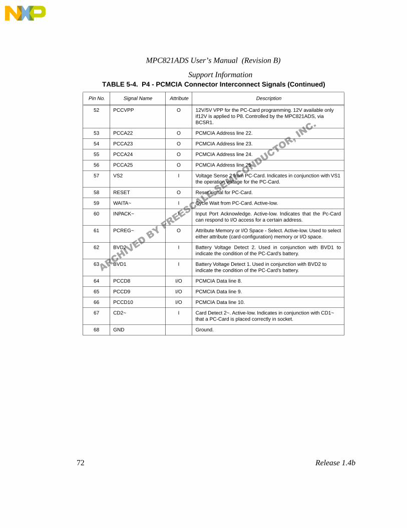
MPC821ADS User’s Manual (Revision B)
72
Release 1.4b
Support Information
52 PCCVPP O 12V/5V VPP for the PC-Card programming. 12V available only if12V is applied to P8. Controlled by the MPC821ADS, via BCSR1.
53 PCCA22 O PCMCIA Address line 22.
54 PCCA23 O PCMCIA Address line 23.
55 PCCA24 O PCMCIA Address line 24.
56 PCCA25 O PCMCIA Address line 25.
57 VS2 I Voltage Sense 2 from PC-Card. Indicates in conjunction with VS1 the operation voltage for the PC-Card.
58 RESET O Reset signal for PC-Card.
59 WAITA~ I Cycle Wait from PC-Card. Active-low.
60 INPACK~ I Input Port Acknowledge. Active-low. Indicates that the Pc-Cardcan respond to I/O access for a certain address.
61 PCREG~ O Attribute Memory or I/O Space - Select. Active-low. Used to selecteither attribute (card-configuration) memory or I/O space.
62 BVD2 I Battery Voltage Detect 2. Used in conjunction with BVD1 toindicate the condition of the PC-Card’s battery.
63 BVD1 I Battery Voltage Detect 1. Used in conjunction with BVD2 to indicate the condition of the PC-Card’s battery.
64 PCCD8 I/O PCMCIA Data line 8.
65 PCCD9 I/O PCMCIA Data line 9.
66 PCCD10 I/O PCMCIA Data line 10.
67 CD2~ I Card Detect 2~. Active-low. Indicates in conjunction with CD1~ that a PC-Card is placed correctly in socket.
68 GND Ground.
TABLE 5-4. P4 - PCMCIA Connector Interconnect Signals (Continued)
Pin No. Signal Name Attribute Description
ARCHIVED BY FREESCALE SEMICONDUCTOR, INC.
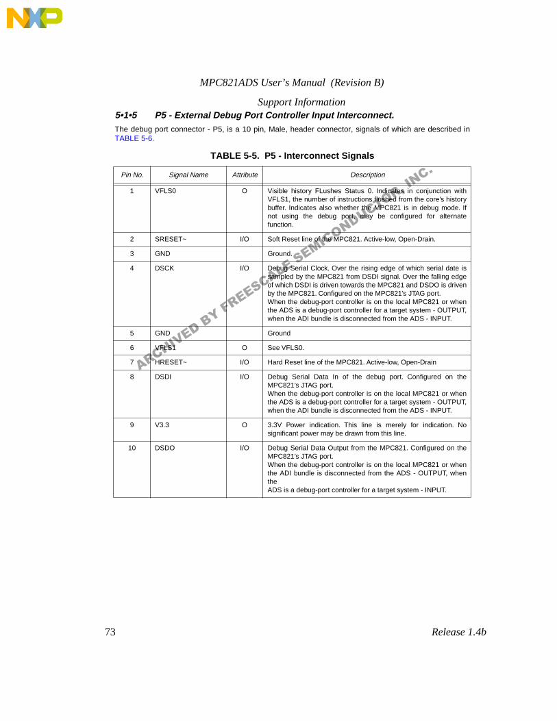
MPC821ADS User’s Manual (Revision B)
73
Release 1.4b
Support Information
5•1•5 P5 - External Debug Port Controller Input Interconnect.
The debug port connector - P5, is a 10 pin, Male, header connector, signals of which are described inTABLE 5-6.
TABLE 5-5. P5 - Interconnect Signals
Pin No. Signal Name Attribute Description
1 VFLS0 O Visible history FLushes Status 0. Indicates in conjunction withVFLS1, the number of instructions flushed from the core’s historybuffer. Indicates also whether the MPC821 is in debug mode. Ifnot using the debug port, may be configured for alternatefunction.
2 SRESET~ I/O Soft Reset line of the MPC821. Active-low, Open-Drain.
3 GND Ground.
4 DSCK I/O Debug Serial Clock. Over the rising edge of which serial date issampled by the MPC821 from DSDI signal. Over the falling edgeof which DSDI is driven towards the MPC821 and DSDO is drivenby the MPC821. Configured on the MPC821’s JTAG port.When the debug-port controller is on the local MPC821 or whenthe ADS is a debug-port controller for a target system - OUTPUT,when the ADI bundle is disconnected from the ADS - INPUT.
5 GND Ground
6 VFLS1 O See VFLS0.
7 HRESET~ I/O Hard Reset line of the MPC821. Active-low, Open-Drain
8 DSDI I/O Debug Serial Data In of the debug port. Configured on theMPC821’s JTAG port. When the debug-port controller is on the local MPC821 or whenthe ADS is a debug-port controller for a target system - OUTPUT,when the ADI bundle is disconnected from the ADS - INPUT.
9 V3.3 O 3.3V Power indication. This line is merely for indication. Nosignificant power may be drawn from this line.
10 DSDO I/O Debug Serial Data Output from the MPC821. Configured on theMPC821’s JTAG port.When the debug-port controller is on the local MPC821 or whenthe ADI bundle is disconnected from the ADS - OUTPUT, whenthe ADS is a debug-port controller for a target system - INPUT.
ARCHIVED BY FREESCALE SEMICONDUCTOR, INC.

MPC821ADS User’s Manual (Revision B)
74
Release 1.4b
Support Information
5•1•6 P6, P9, P10 & P12 Expansion and Logic Analyzer Connectors.
Each of these connectors is composed of quad SMD pin-rows. P6 has a 120 pin-count while the rest have100 pin count. All MPC821 pins appear in these connectors plus few auxiliary control pins. These connec-tors are arranged in a quadratic assembly around the MPC821 to provide short PCB routs. The connectorsassembly is shown in FIGURE 5-1 "Expansion Connector Assembly" on page 75. The interconnect signalsof the connectors are described in TABLE 5-6. "P6 - Interconnect Signals" on page 75, in TABLE 5-6. "P6- Interconnect Signals" on page 75, in TABLE 5-8. "P10 - Interconnect Signals" on page 86 and in TABLE5-9. "P12 - Interconnect Signals" on page 91.
5•1•6•1 Connecting Application Boards to the Expansion Connectors
The expansion connectors P6, P9, P10 & P12 are arranged in a way that allows for wire-wrap boards tobe connected to it, i.e., connectors’ pins are located on a 0.1" snap grid, as shown in FIGURE 5-1. Anyboard that is to be attached to these connectors, should have a rectangle hole in its center, so that theMPC821 socket may be accessed. The recommended hole size is shown in FIGURE 5-1 as well.
Connecting an application board to the expansion connectors, requires the following connectors, to matchthe ADS’s connectors:
• 6 units of - Socket-strip, double-row Wire-Wrap, 50 pin (25 X 2 rows), female, straight. E.g.:SSQ12524GD by Samtec.
• 2 units of - Socket-strip, double-row Wire-Wrap, 60 pin (30 X 2 rows), female, straight. E.g.: SSQ13024GD by Samtec.
Using WW connectors even on a printed card, retains logic analyzer connection capability.
ARCHIVED BY FREESCALE SEMICONDUCTOR, INC.
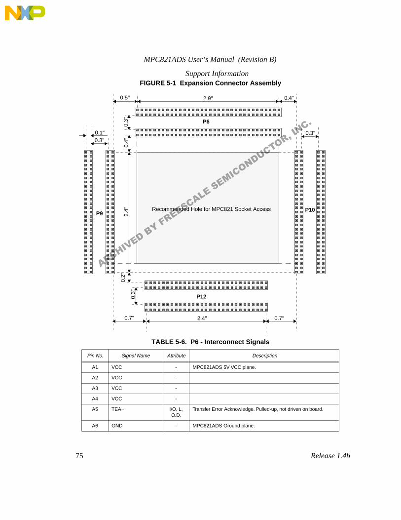
MPC821ADS User’s Manual (Revision B)
75
Release 1.4b
Support Information
FIGURE 5-1 Expansion Connector Assembly
TABLE 5-6. P6 - Interconnect Signals
Pin No. Signal Name Attribute Description
A1 VCC - MPC821ADS 5V VCC plane.
A2 VCC -
A3 VCC -
A4 VCC -
A5 TEA~ I/O, L, O.D.
Transfer Error Acknowledge. Pulled-up, not driven on board.
A6 GND - MPC821ADS Ground plane.
P6
P9P10
P12
0.1"
0.5" 2.9" 0.4"
0.3"0.
4"2.
4"0.
2"
0.7" 2.4" 0.7"
0.3"
0.3"
0.3"
Recommended Hole for MPC821 Socket Access
ARCHIVED BY FREESCALE SEMICONDUCTOR, INC.
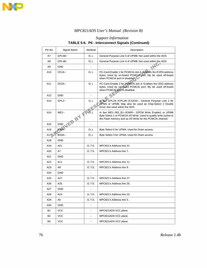
MPC821ADS User’s Manual (Revision B)
76
Release 1.4b
Support Information
A7 GPL5B~ O, L General Purpose Line 5 of UPMB. Not used within the ADS.
A8 GPL4B~ O, L General Purpose Line 4 of UPMB. Not used within the ADS.
A9 GND - .
A10 CE1A~ O, L PC-Card Enable 1 for PCMCIA slot A. Enables the EVEN addressbytes. Used by on-board PCMCIA port. My be used off-boardwhen PCMCIA port in disabled.
A11 CE2A~ O, L PC-Card Enable 2 for PCMCIA slot A. Enables the ODD addressbytes. Used by on-board PCMCIA port. My be used off-boardwhen PCMCIA port in disabled.
A12 GND -
A13 GPL2~ O, L In fact GPL2A~/GPL2B~/CS2DD~. General Purpose Line 2 forUPMA or UPMB. May also be used as Chip-Select 2 DoubleDrive. Not used within the ADS.
A14 WE1~ O, L In fact WE1~/BS_B1~/IOWR~. GPCM Write Enable1 or UPMBByte Select 1 or PCMCIA I/O Write. Used to qualify write cycles tothe Flash memory and as I/O Write for the PCMCIA channel.
A15 GND -
A16 BS0A~ O, L Byte Select 0 for UPMA. Used for Dram access.
A17 BS3A~ O, L Byte Select 3 for UPMA. Used for Dram access.
A18 GND -
A19 A21 O, T.S. MPC821’s Address line 21.
A20 A7 O, T.S. MPC821’s Address line 7.
A21 GND
A22 A11 O, T.S. MPC821’s Address line 11.
A23 A9 O, T.S. MPC821’s Address line 9.
A24 GND -
A25 A27 O, T.S. MPC821’s Address line 27.
A26 A25 O, T.S. MPC821’s Address line 25.
A27 GND -
A28 A23 O, T.S. MPC821’s Address line 23.
A29 A5 O, T.S. MPC821’s Address line 5.
A30 GND -
B1 VCC - MPC821ADS VCC plane.
B2 VCC - MPC821ADS VCC plane.
B3 VCC - MPC821ADS VCC plane.
TABLE 5-6. P6 - Interconnect Signals (Continued)
Pin No. Signal Name Attribute Description
ARCHIVED BY FREESCALE SEMICONDUCTOR, INC.
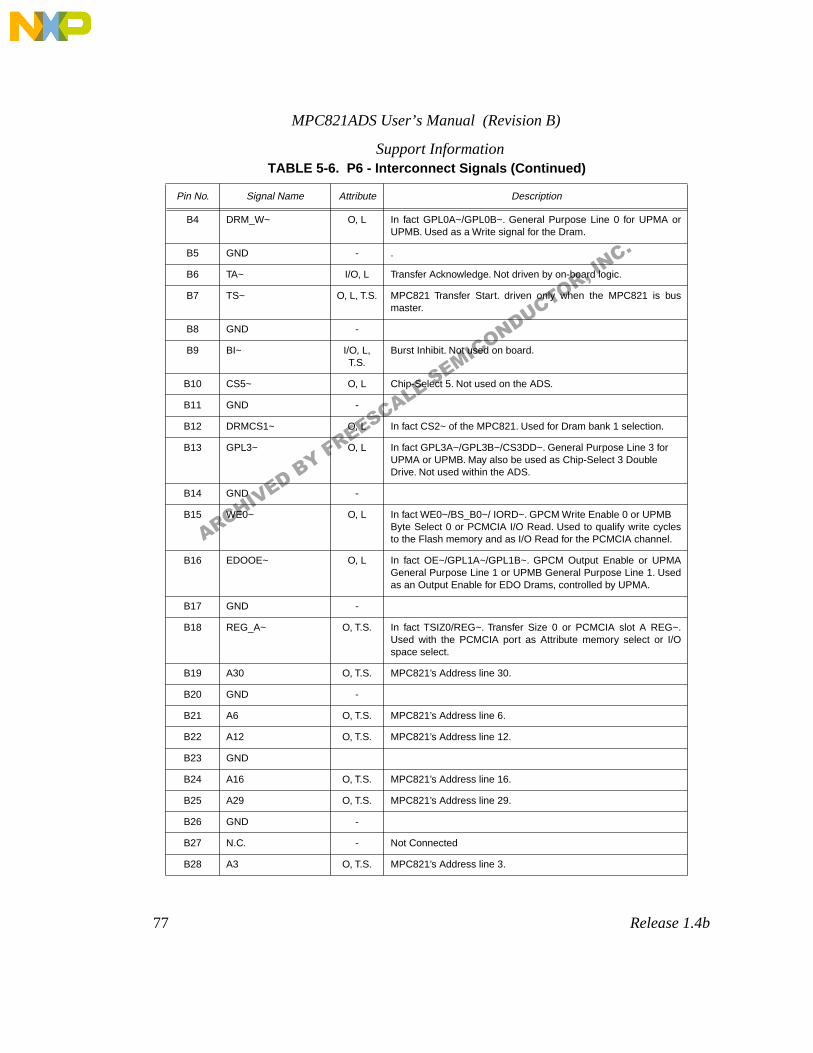
MPC821ADS User’s Manual (Revision B)
77
Release 1.4b
Support Information
B4 DRM_W~ O, L In fact GPL0A~/GPL0B~. General Purpose Line 0 for UPMA orUPMB. Used as a Write signal for the Dram.
B5 GND - .
B6 TA~ I/O, L Transfer Acknowledge. Not driven by on-board logic.
B7 TS~ O, L, T.S. MPC821 Transfer Start. driven only when the MPC821 is busmaster.
B8 GND -
B9 BI~ I/O, L, T.S.
Burst Inhibit. Not used on board.
B10 CS5~ O, L Chip-Select 5. Not used on the ADS.
B11 GND -
B12 DRMCS1~ O, L In fact CS2~ of the MPC821. Used for Dram bank 1 selection.
B13 GPL3~ O, L In fact GPL3A~/GPL3B~/CS3DD~. General Purpose Line 3 for UPMA or UPMB. May also be used as Chip-Select 3 Double Drive. Not used within the ADS.
B14 GND -
B15 WE0~ O, L In fact WE0~/BS_B0~/ IORD~. GPCM Write Enable 0 or UPMB Byte Select 0 or PCMCIA I/O Read. Used to qualify write cyclesto the Flash memory and as I/O Read for the PCMCIA channel.
B16 EDOOE~ O, L In fact OE~/GPL1A~/GPL1B~. GPCM Output Enable or UPMAGeneral Purpose Line 1 or UPMB General Purpose Line 1. Usedas an Output Enable for EDO Drams, controlled by UPMA.
B17 GND -
B18 REG_A~ O, T.S. In fact TSIZ0/REG~. Transfer Size 0 or PCMCIA slot A REG~.Used with the PCMCIA port as Attribute memory select or I/Ospace select.
B19 A30 O, T.S. MPC821’s Address line 30.
B20 GND -
B21 A6 O, T.S. MPC821’s Address line 6.
B22 A12 O, T.S. MPC821’s Address line 12.
B23 GND
B24 A16 O, T.S. MPC821’s Address line 16.
B25 A29 O, T.S. MPC821’s Address line 29.
B26 GND -
B27 N.C. - Not Connected
B28 A3 O, T.S. MPC821’s Address line 3.
TABLE 5-6. P6 - Interconnect Signals (Continued)
Pin No. Signal Name Attribute Description
ARCHIVED BY FREESCALE SEMICONDUCTOR, INC.
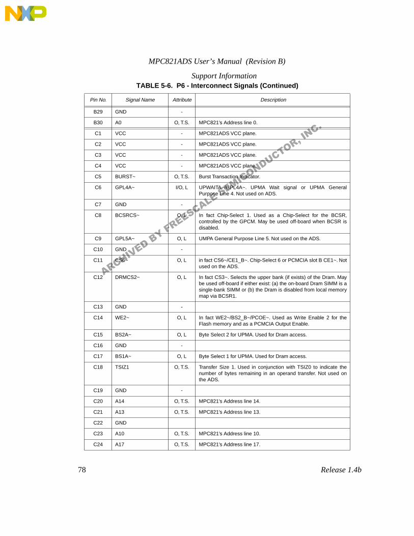
MPC821ADS User’s Manual (Revision B)
78
Release 1.4b
Support Information
B29 GND -
B30 A0 O, T.S. MPC821’s Address line 0.
C1 VCC - MPC821ADS VCC plane.
C2 VCC - MPC821ADS VCC plane.
C3 VCC - MPC821ADS VCC plane.
C4 VCC - MPC821ADS VCC plane.
C5 BURST~ O, T.S. Burst Transaction Indicator.
C6 GPL4A~ I/O, L UPWAITA~/GPL4A~. UPMA Wait signal or UPMA GeneralPurpose Line 4. Not used on ADS.
C7 GND -
C8 BCSRCS~ O, L In fact Chip-Select 1. Used as a Chip-Select for the BCSR,controlled by the GPCM. May be used off-board when BCSR isdisabled.
C9 GPL5A~ O, L UMPA General Purpose Line 5. Not used on the ADS.
C10 GND -
C11 CS6~ O, L in fact CS6~/CE1_B~. Chip-Select 6 or PCMCIA slot B CE1~. Notused on the ADS.
C12 DRMCS2~ O, L In fact CS3~. Selects the upper bank (if exists) of the Dram. Maybe used off-board if either exist: (a) the on-board Dram SIMM is asingle-bank SIMM or (b) the Dram is disabled from local memorymap via BCSR1.
C13 GND -
C14 WE2~ O, L In fact WE2~/BS2_B~/PCOE~. Used as Write Enable 2 for theFlash memory and as a PCMCIA Output Enable.
C15 BS2A~ O, L Byte Select 2 for UPMA. Used for Dram access.
C16 GND -
C17 BS1A~ O, L Byte Select 1 for UPMA. Used for Dram access.
C18 TSIZ1 O, T.S. Transfer Size 1. Used in conjunction with TSIZ0 to indicate thenumber of bytes remaining in an operand transfer. Not used onthe ADS.
C19 GND -
C20 A14 O, T.S. MPC821’s Address line 14.
C21 A13 O, T.S. MPC821’s Address line 13.
C22 GND
C23 A10 O, T.S. MPC821’s Address line 10.
C24 A17 O, T.S. MPC821’s Address line 17.
TABLE 5-6. P6 - Interconnect Signals (Continued)
Pin No. Signal Name Attribute Description
ARCHIVED BY FREESCALE SEMICONDUCTOR, INC.
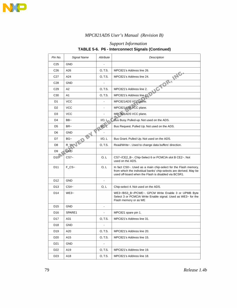
MPC821ADS User’s Manual (Revision B)
79
Release 1.4b
Support Information
C25 GND -
C26 A26 O, T.S. MPC821’s Address line 26.
C27 A24 O, T.S. MPC821’s Address line 24.
C28 GND -
C29 A2 O, T.S. MPC821’s Address line 2.
C30 A1 O, T.S. MPC821’s Address line 1.
D1 VCC - MPC821ADS VCC plane.
D2 VCC - MPC821ADS VCC plane.
D3 VCC - MPC821ADS VCC plane.
D4 BB~ I/O, L Bus Busy. Pulled-up. Not used on the ADS.
D5 BR~ I/O, L Bus Request. Pulled Up. Not used on the ADS.
D6 GND -
D7 BG~ I/O, L Bus Grant. Pulled Up. Not used on the ADS.
D8 R_W~ O, T.S. Read/Write~. Used to change data buffers’ direction.
D9 GND
D10 CS7~ O, L CS7~/CE2_B~. Chip-Select 6 or PCMCIA slot B CE2~. Not used on the ADS.
D11 F_CS~ O, L In fact CS0~. Used as a main chip-select for the Flash memory,from which the individual banks’ chip-selects are derived. May beused off-board when the Flash is disabled via BCSR1.
D12 GND -
D13 CS4~ O, L Chip-select 4. Not used on the ADS.
D14 WE3~ WE3~/BS3_B~/PCWE~. GPCM Write Enable 3 or UPMB ByteSelect 3 or PCMCIA Write Enable signal. Used as WE3~ for theFlash memory or as WE
D15 GND -
D16 SPARE1 - MPC821 spare pin 1.
D17 A31 O, T.S. MPC821’s Address line 31.
D18 GND -
D19 A20 O, T.S. MPC821’s Address line 20.
D20 A15 O, T.S. MPC821’s Address line 15.
D21 GND -
D22 A19 O, T.S. MPC821’s Address line 19.
D23 A18 O, T.S. MPC821’s Address line 18.
TABLE 5-6. P6 - Interconnect Signals (Continued)
Pin No. Signal Name Attribute Description
ARCHIVED BY FREESCALE SEMICONDUCTOR, INC.
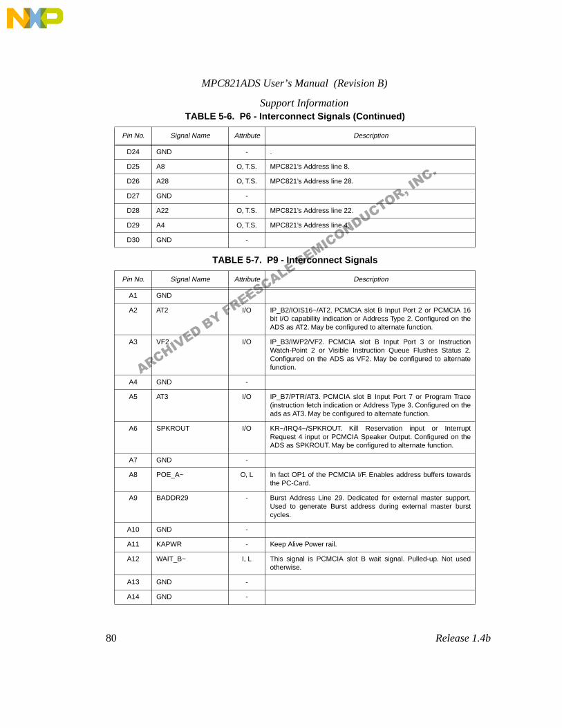
MPC821ADS User’s Manual (Revision B)
80
Release 1.4b
Support Information
D24 GND - .
D25 A8 O, T.S. MPC821’s Address line 8.
D26 A28 O, T.S. MPC821’s Address line 28.
D27 GND -
D28 A22 O, T.S. MPC821’s Address line 22.
D29 A4 O, T.S. MPC821’s Address line 4.
D30 GND -
TABLE 5-7. P9 - Interconnect Signals
Pin No. Signal Name Attribute Description
A1 GND -
A2 AT2 I/O IP_B2/IOIS16~/AT2. PCMCIA slot B Input Port 2 or PCMCIA 16bit I/O capability indication or Address Type 2. Configured on theADS as AT2. May be configured to alternate function.
A3 VF2 I/O IP_B3/IWP2/VF2. PCMCIA slot B Input Port 3 or InstructionWatch-Point 2 or Visible Instruction Queue Flushes Status 2.Configured on the ADS as VF2. May be configured to alternatefunction.
A4 GND -
A5 AT3 I/O IP_B7/PTR/AT3. PCMCIA slot B Input Port 7 or Program Trace(instruction fetch indication or Address Type 3. Configured on theads as AT3. May be configured to alternate function.
A6 SPKROUT I/O KR~/IRQ4~/SPKROUT. Kill Reservation input or InterruptRequest 4 input or PCMCIA Speaker Output. Configured on theADS as SPKROUT. May be configured to alternate function.
A7 GND -
A8 POE_A~ O, L In fact OP1 of the PCMCIA I/F. Enables address buffers towardsthe PC-Card.
A9 BADDR29 - Burst Address Line 29. Dedicated for external master support.Used to generate Burst address during external master burstcycles.
A10 GND -
A11 KAPWR - Keep Alive Power rail.
A12 WAIT_B~ I, L This signal is PCMCIA slot B wait signal. Pulled-up. Not usedotherwise.
A13 GND -
A14 GND -
TABLE 5-6. P6 - Interconnect Signals (Continued)
Pin No. Signal Name Attribute Description
ARCHIVED BY FREESCALE SEMICONDUCTOR, INC.
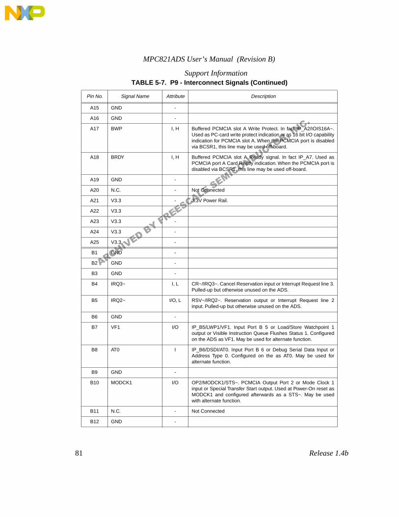
MPC821ADS User’s Manual (Revision B)
81
Release 1.4b
Support Information
A15 GND -
A16 GND -
A17 BWP I, H Buffered PCMCIA slot A Write Protect. In fact IP_A2/IOIS16A~.Used as PC-card write protect indication or as 16 bit I/O capabilityindication for PCMCIA slot A. When the PCMCIA port is disabledvia BCSR1, this line may be used off-board.
A18 BRDY I, H Buffered PCMCIA slot A Ready signal. In fact IP_A7. Used asPCMCIA port A Card Ready indication. When the PCMCIA port isdisabled via BCSR1, this line may be used off-board.
A19 GND -
A20 N.C. - Not Connected
A21 V3.3 - 3.3V Power Rail.
A22 V3.3 -
A23 V3.3 -
A24 V3.3 -
A25 V3.3 -
B1 GND -
B2 GND -
B3 GND -
B4 IRQ3~ I, L CR~/IRQ3~. Cancel Reservation input or Interrupt Request line 3.Pulled-up but otherwise unused on the ADS.
B5 IRQ2~ I/O, L RSV~/IRQ2~. Reservation output or Interrupt Request line 2input. Pulled-up but otherwise unused on the ADS.
B6 GND -
B7 VF1 I/O IP_B5/LWP1/VF1. Input Port B 5 or Load/Store Watchpoint 1output or Visible Instruction Queue Flushes Status 1. Configuredon the ADS as VF1. May be used for alternate function.
B8 AT0 I IP_B6/DSDI/AT0. Input Port B 6 or Debug Serial Data Input orAddress Type 0. Configured on the as AT0. May be used foralternate function.
B9 GND -
B10 MODCK1 I/O OP2/MODCK1/STS~. PCMCIA Output Port 2 or Mode Clock 1input or Special Transfer Start output. Used at Power-On reset asMODCK1 and configured afterwards as a STS~. May be usedwith alternate function.
B11 N.C. - Not Connected
B12 GND -
TABLE 5-7. P9 - Interconnect Signals (Continued)
Pin No. Signal Name Attribute Description
ARCHIVED BY FREESCALE SEMICONDUCTOR, INC.
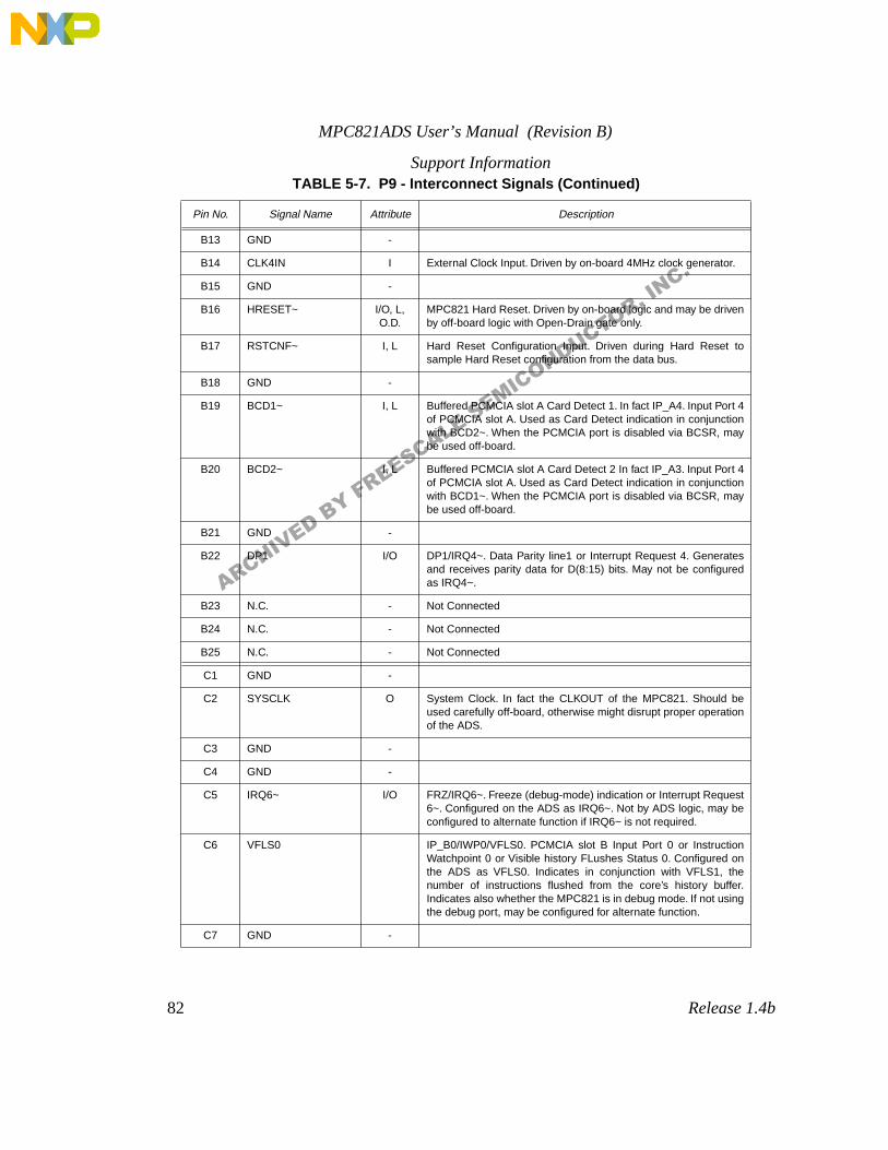
MPC821ADS User’s Manual (Revision B)
82
Release 1.4b
Support Information
B13 GND -
B14 CLK4IN I External Clock Input. Driven by on-board 4MHz clock generator.
B15 GND -
B16 HRESET~ I/O, L, O.D.
MPC821 Hard Reset. Driven by on-board logic and may be drivenby off-board logic with Open-Drain gate only.
B17 RSTCNF~ I, L Hard Reset Configuration Input. Driven during Hard Reset tosample Hard Reset configuration from the data bus.
B18 GND -
B19 BCD1~ I, L Buffered PCMCIA slot A Card Detect 1. In fact IP_A4. Input Port 4of PCMCIA slot A. Used as Card Detect indication in conjunctionwith BCD2~. When the PCMCIA port is disabled via BCSR, maybe used off-board.
B20 BCD2~ I, L Buffered PCMCIA slot A Card Detect 2 In fact IP_A3. Input Port 4of PCMCIA slot A. Used as Card Detect indication in conjunctionwith BCD1~. When the PCMCIA port is disabled via BCSR, maybe used off-board.
B21 GND -
B22 DP1 I/O DP1/IRQ4~. Data Parity line1 or Interrupt Request 4. Generatesand receives parity data for D(8:15) bits. May not be configuredas IRQ4~.
B23 N.C. - Not Connected
B24 N.C. - Not Connected
B25 N.C. - Not Connected
C1 GND -
C2 SYSCLK O System Clock. In fact the CLKOUT of the MPC821. Should beused carefully off-board, otherwise might disrupt proper operationof the ADS.
C3 GND -
C4 GND -
C5 IRQ6~ I/O FRZ/IRQ6~. Freeze (debug-mode) indication or Interrupt Request6~. Configured on the ADS as IRQ6~. Not by ADS logic, may beconfigured to alternate function if IRQ6~ is not required.
C6 VFLS0 IP_B0/IWP0/VFLS0. PCMCIA slot B Input Port 0 or InstructionWatchpoint 0 or Visible history FLushes Status 0. Configured onthe ADS as VFLS0. Indicates in conjunction with VFLS1, thenumber of instructions flushed from the core’s history buffer.Indicates also whether the MPC821 is in debug mode. If not usingthe debug port, may be configured for alternate function.
C7 GND -
TABLE 5-7. P9 - Interconnect Signals (Continued)
Pin No. Signal Name Attribute Description
ARCHIVED BY FREESCALE SEMICONDUCTOR, INC.
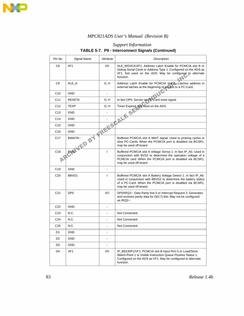
MPC821ADS User’s Manual (Revision B)
83
Release 1.4b
Support Information
C8 AT1 I/O ALE_B/DSCK/AT1. Address Latch Enable for PCMCIA slot B orDebug Serial Clock or Address Type 1. Configured on the ADS asAT1. Not used on the ADS. May be configured to alternatefunction.
C9 ALE_A O, H Address Latch Enable for PCMCIA slot A. Latches address inexternal latches at the beginning of access to a PC-Card.
C10 GND -
C11 RESETA O, H In fact OP0. Serves as PC-Card reset signal.
C12 TEXP O, H Timer Expired. Not used on the ADS.
C13 GND -
C14 GND -
C15 GND -
C16 GND -
C17 BWAITA~ Buffered PCMCIA slot A WAIT signal. Used to prolong cycles toslow PC-Cards. When the PCMCIA port is disabled via BCSR1,may be used off-board.
C18 BVS1 I Buffered PCMCIA slot A Voltage Sense 1. In fact IP_A0. Used inconjunction with BVS2 to determine the operation voltage of aPCMCIA card. When the PCMCIA port is disabled via BCSR1,may be used off-board.
C19 GND -
C20 BBVD1 I Buffered PCMCIA slot A Battery Voltage Detect 1. In fact IP_A6.Used in conjunction with BBVD2 to determine the battery statusof a PC-Card. When the PCMCIA port is disabled via BCSR1,may be used off-board.
C21 DP0 I/O DP0/IRQ3~. Data Parity line 0 or Interrupt Request 3. Generates and receives parity data for D(0:7) bits. May not be configured as IRQ3~.
C22 GND -
C23 N.C. - Not Connected.
C24 N.C. - Not Connected.
C25 N.C. - Not Connected.
D1 GND -
D2 GND -
D3 GND -
D4 VF1 I/O IP_B5/LWP1/VF1. PCMCIA slot B Input Port 5 or Load/Store Watch-Point 1 or Visible Instruction Queue Flushes Status 1. Configured on the ADS as VF1. May be configured to alternate function.
TABLE 5-7. P9 - Interconnect Signals (Continued)
Pin No. Signal Name Attribute Description
ARCHIVED BY FREESCALE SEMICONDUCTOR, INC.
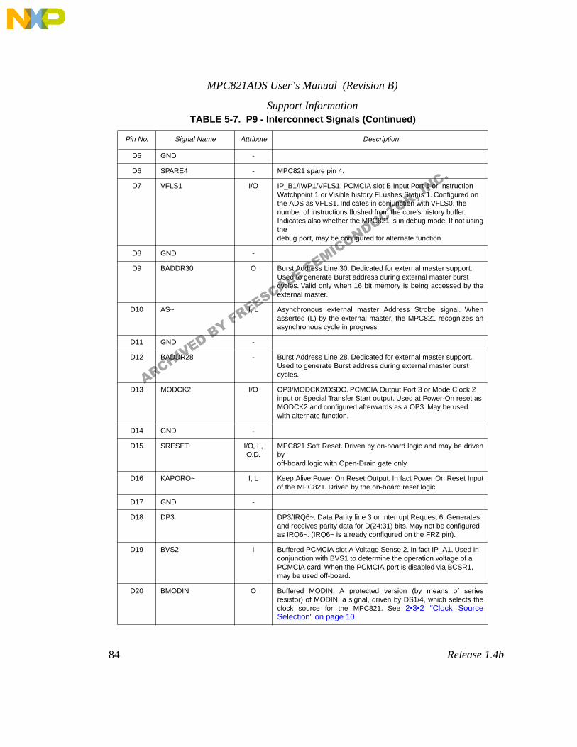
MPC821ADS User’s Manual (Revision B)
84
Release 1.4b
Support Information
D5 GND -
D6 SPARE4 - MPC821 spare pin 4.
D7 VFLS1 I/O IP_B1/IWP1/VFLS1. PCMCIA slot B Input Port 1 or Instruction Watchpoint 1 or Visible history FLushes Status 1. Configured on the ADS as VFLS1. Indicates in conjunction with VFLS0, the number of instructions flushed from the core’s history buffer. Indicates also whether the MPC821 is in debug mode. If not usingthe debug port, may be configured for alternate function.
D8 GND -
D9 BADDR30 O Burst Address Line 30. Dedicated for external master support. Used to generate Burst address during external master burst cycles. Valid only when 16 bit memory is being accessed by theexternal master.
D10 AS~ I, L Asynchronous external master Address Strobe signal. Whenasserted (L) by the external master, the MPC821 recognizes anasynchronous cycle in progress.
D11 GND -
D12 BADDR28 - Burst Address Line 28. Dedicated for external master support. Used to generate Burst address during external master burst cycles.
D13 MODCK2 I/O OP3/MODCK2/DSDO. PCMCIA Output Port 3 or Mode Clock 2 input or Special Transfer Start output. Used at Power-On reset as MODCK2 and configured afterwards as a OP3. May be used with alternate function.
D14 GND -
D15 SRESET~ I/O, L, O.D.
MPC821 Soft Reset. Driven by on-board logic and may be drivenby off-board logic with Open-Drain gate only.
D16 KAPORO~ I, L Keep Alive Power On Reset Output. In fact Power On Reset Inputof the MPC821. Driven by the on-board reset logic.
D17 GND -
D18 DP3 DP3/IRQ6~. Data Parity line 3 or Interrupt Request 6. Generates and receives parity data for D(24:31) bits. May not be configured as IRQ6~. (IRQ6~ is already configured on the FRZ pin).
D19 BVS2 I Buffered PCMCIA slot A Voltage Sense 2. In fact IP_A1. Used in conjunction with BVS1 to determine the operation voltage of a PCMCIA card. When the PCMCIA port is disabled via BCSR1, may be used off-board.
D20 BMODIN O Buffered MODIN. A protected version (by means of seriesresistor) of MODIN, a signal, driven by DS1/4, which selects theclock source for the MPC821. See
2•3•2 "Clock SourceSelection" on page 10
.
TABLE 5-7. P9 - Interconnect Signals (Continued)
Pin No. Signal Name Attribute Description
ARCHIVED BY FREESCALE SEMICONDUCTOR, INC.
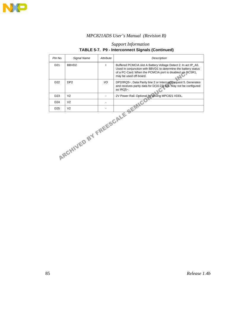
MPC821ADS User’s Manual (Revision B)
85
Release 1.4b
Support Information
D21 BBVD2 I Buffered PCMCIA slot A Battery Voltage Detect 2. In act IP_A5. Used in conjunction with BBVD1 to determine the battery status of a PC-Card. When the PCMCIA port is disabled via BCSR1, may be used off-board.
D22 DP2 I/O DP2/IRQ5~. Data Parity line 2 or Interrupt Request 5. Generates and receives parity data for D(16:23) bits. May not be configured as IRQ5~.
D23 V2 - 2V Power Rail. Optional for driving MPC821 VDDL.
D24 V2 -
D25 V2 -
TABLE 5-7. P9 - Interconnect Signals (Continued)
Pin No. Signal Name Attribute Description
ARCHIVED BY FREESCALE SEMICONDUCTOR, INC.
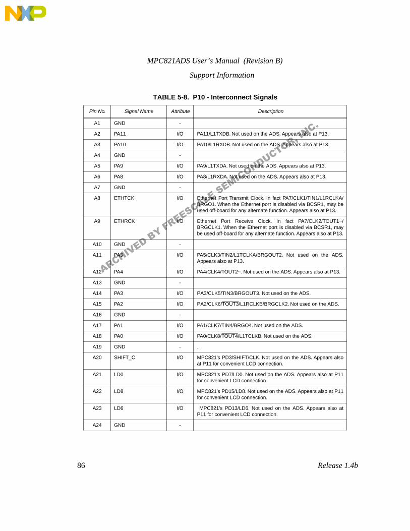
MPC821ADS User’s Manual (Revision B)
86
Release 1.4b
Support Information
TABLE 5-8. P10 - Interconnect Signals
Pin No. Signal Name Attribute Description
A1 GND -
A2 PA11 I/O PA11/L1TXDB. Not used on the ADS. Appears also at P13.
A3 PA10 I/O PA10/L1RXDB. Not used on the ADS. Appears also at P13.
A4 GND -
A5 PA9 I/O PA9/L1TXDA. Not used on the ADS. Appears also at P13.
A6 PA8 I/O PA8/L1RXDA. Not used on the ADS. Appears also at P13.
A7 GND -
A8 ETHTCK I/O Ethernet Port Transmit Clock. In fact PA7/CLK1/TIN1/L1RCLKA/BRGO1. When the Ethernet port is disabled via BCSR1, may beused off-board for any alternate function. Appears also at P13.
A9 ETHRCK I/O Ethernet Port Receive Clock. In fact PA7/CLK2/TOUT1~/BRGCLK1. When the Ethernet port is disabled via BCSR1, maybe used off-board for any alternate function. Appears also at P13.
A10 GND -
A11 PA5 I/O PA5/CLK3/TIN2/L1TCLKA/BRGOUT2. Not used on the ADS.Appears also at P13.
A12 PA4 I/O PA4/CLK4/TOUT2~. Not used on the ADS. Appears also at P13.
A13 GND -
A14 PA3 I/O PA3/CLK5/TIN3/BRGOUT3. Not used on the ADS.
A15 PA2 I/O PA2/CLK6/TOUT3/L1RCLKB/BRGCLK2. Not used on the ADS.
A16 GND -
A17 PA1 I/O PA1/CLK7/TIN4/BRGO4. Not used on the ADS.
A18 PA0 I/O PA0/CLK8/TOUT4/L1TCLKB. Not used on the ADS.
A19 GND - .
A20 SHIFT_C I/O MPC821’s PD3/SHIFT/CLK. Not used on the ADS. Appears alsoat P11 for convenient LCD connection.
A21 LD0 I/O MPC821’s PD7/LD0. Not used on the ADS. Appears also at P11for convenient LCD connection.
A22 LD8 I/O MPC821’s PD15/LD8. Not used on the ADS. Appears also at P11for convenient LCD connection.
A23 LD6 I/O MPC821’s PD13/LD6. Not used on the ADS. Appears also atP11 for convenient LCD connection.
A24 GND -
ARCHIVED BY FREESCALE SEMICONDUCTOR, INC.
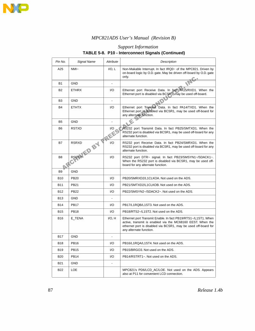
MPC821ADS User’s Manual (Revision B)
87
Release 1.4b
Support Information
A25 NMI~ I/O, L Non-Makable Interrupt. In fact IRQ0~ of the MPC821. Driven byon-board logic by O.D. gate. May be driven off-board by O.D. gateonly.
B1 GND -
B2 ETHRX I/O Ethernet port Receive Data. In fact PA15/RXD1. When theEthernet port is disabled via BCSR1, may be used off-board.
B3 GND -
B4 ETHTX I/O Ethernet port Transmit Data. In fact PA14/TXD1. When theEthernet port is disabled via BCSR1, may be used off-board forany alternate function.
B5 GND -
B6 RSTXD I/O RS232 port Transmit Data. In fact PB25/SMTXD1. When theRS232 port is disabled via BCSR1, may be used off-board for anyalternate function.
B7 RSRXD I/O RS232 port Receive Data. In fact PB24/SMRXD1. When theRS232 port is disabled via BCSR1, may be used off-board for anyalternate function.
B8 RSDTR~ I/O RS232 port DTR~ signal. In fact PB23/SMSYN1~/SDACK1~.When the RS232 port is disabled via BCSR1, may be used off-board for any alternate function.
B9 GND
B10 PB20 I/O PB20/SMRXD2/L1CLKOA. Not used on the ADS.
B11 PB21 I/O PB21/SMTXD2/L1CLKOB. Not used on the ADS.
B12 PB22 I/O PB22/SMSYN2~/SDACK2~. Not used on the ADS.
B13 GND -
B14 PB17 I/O PB17/L1RQB/L1ST3. Not used on the ADS.
B15 PB18 I/O PB18/RTS2~/L1ST2. Not used on the ADS.
B16 E_TENA I/O, H Ethernet port Transmit Enable. In fact PB19/RTS1~/L1ST1. Whenactive, transmit is enabled via the MC68160 EEST. When theethernet port is disabled via BCSR1, may be used off-board forany alternate function.
B17 GND -
B18 PB16 I/O PB16/L1RQA/L1ST4. Not used on the ADS.
B19 PB15 I/O PB15/BRGO3. Not used on the ADS.
B20 PB14 I/O PB14/RSTRT1~. Not used on the ADS.
B21 GND -
B22 LOE MPC821’s PD6/LCD_AC/LOE. Not used on the ADS. Appearsalso at P11 for convenient LCD connection.
TABLE 5-8. P10 - Interconnect Signals (Continued)
Pin No. Signal Name Attribute Description
ARCHIVED BY FREESCALE SEMICONDUCTOR, INC.
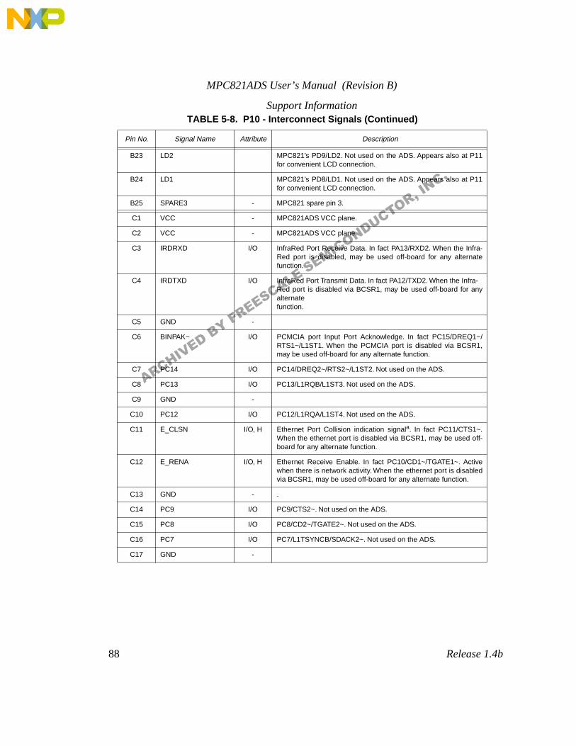
MPC821ADS User’s Manual (Revision B)
88
Release 1.4b
Support Information
B23 LD2 MPC821’s PD9/LD2. Not used on the ADS. Appears also at P11for convenient LCD connection.
B24 LD1 MPC821’s PD8/LD1. Not used on the ADS. Appears also at P11for convenient LCD connection.
B25 SPARE3 - MPC821 spare pin 3.
C1 VCC - MPC821ADS VCC plane.
C2 VCC - MPC821ADS VCC plane.
C3 IRDRXD I/O InfraRed Port Receive Data. In fact PA13/RXD2. When the Infra-Red port is disabled, may be used off-board for any alternatefunction.
C4 IRDTXD I/O InfraRed Port Transmit Data. In fact PA12/TXD2. When the Infra-Red port is disabled via BCSR1, may be used off-board for anyalternate function.
C5 GND -
C6 BINPAK~ I/O PCMCIA port Input Port Acknowledge. In fact PC15/DREQ1~/RTS1~/L1ST1. When the PCMCIA port is disabled via BCSR1,may be used off-board for any alternate function.
C7 PC14 I/O PC14/DREQ2~/RTS2~/L1ST2. Not used on the ADS.
C8 PC13 I/O PC13/L1RQB/L1ST3. Not used on the ADS.
C9 GND -
C10 PC12 I/O PC12/L1RQA/L1ST4. Not used on the ADS.
C11 E_CLSN I/O, H Ethernet Port Collision indication signal
a
. In fact PC11/CTS1~.When the ethernet port is disabled via BCSR1, may be used off-board for any alternate function.
C12 E_RENA I/O, H Ethernet Receive Enable. In fact PC10/CD1~/TGATE1~. Activewhen there is network activity. When the ethernet port is disabledvia BCSR1, may be used off-board for any alternate function.
C13 GND - .
C14 PC9 I/O PC9/CTS2~. Not used on the ADS.
C15 PC8 I/O PC8/CD2~/TGATE2~. Not used on the ADS.
C16 PC7 I/O PC7/L1TSYNCB/SDACK2~. Not used on the ADS.
C17 GND -
TABLE 5-8. P10 - Interconnect Signals (Continued)
Pin No. Signal Name Attribute Description
ARCHIVED BY FREESCALE SEMICONDUCTOR, INC.
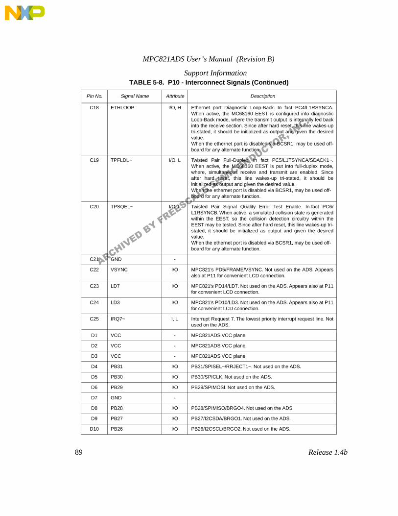
MPC821ADS User’s Manual (Revision B)
89
Release 1.4b
Support Information
C18 ETHLOOP I/O, H Ethernet port Diagnostic Loop-Back. In fact PC4/L1RSYNCA.When active, the MC68160 EEST is configured into diagnosticLoop-Back mode, where the transmit output is internally fed backinto the receive section. Since after hard reset, this line wakes-uptri-stated, it should be initialized as output and given the desiredvalue. When the ethernet port is disabled via BCSR1, may be used off-board for any alternate function.
C19 TPFLDL~ I/O, L Twisted Pair Full-Duplex. In fact PC5/L1TSYNCA/SDACK1~.When active, the MC68160 EEST is put into full-duplex mode,where, simultaneous receive and transmit are enabled. Sinceafter hard reset, this line wakes-up tri-stated, it should beinitialized as output and given the desired value. When the ethernet port is disabled via BCSR1, may be used off-board for any alternate function.
C20 TPSQEL~ I/O, L Twisted Pair Signal Quality Error Test Enable. In-fact PC6/L1RSYNCB. When active, a simulated collision state is generatedwithin the EEST, so the collision detection circuitry within theEEST may be tested. Since after hard reset, this line wakes-up tri-stated, it should be initialized as output and given the desiredvalue. When the ethernet port is disabled via BCSR1, may be used off-board for any alternate function.
C21 GND -
C22 VSYNC I/O MPC821’s PD5/FRAME/VSYNC. Not used on the ADS. Appearsalso at P11 for convenient LCD connection.
C23 LD7 I/O MPC821’s PD14/LD7. Not used on the ADS. Appears also at P11for convenient LCD connection.
C24 LD3 I/O MPC821’s PD10/LD3. Not used on the ADS. Appears also at P11for convenient LCD connection.
C25 IRQ7~ I, L Interrupt Request 7. The lowest priority interrupt request line. Notused on the ADS.
D1 VCC - MPC821ADS VCC plane.
D2 VCC - MPC821ADS VCC plane.
D3 VCC - MPC821ADS VCC plane.
D4 PB31 I/O PB31/SPISEL~/RRJECT1~. Not used on the ADS.
D5 PB30 I/O PB30/SPICLK. Not used on the ADS.
D6 PB29 I/O PB29/SPIMOSI. Not used on the ADS.
D7 GND -
D8 PB28 I/O PB28/SPIMISO/BRGO4. Not used on the ADS.
D9 PB27 I/O PB27/I2CSDA/BRGO1. Not used on the ADS.
D10 PB26 I/O PB26/I2CSCL/BRGO2. Not used on the ADS.
TABLE 5-8. P10 - Interconnect Signals (Continued)
Pin No. Signal Name Attribute Description
ARCHIVED BY FREESCALE SEMICONDUCTOR, INC.
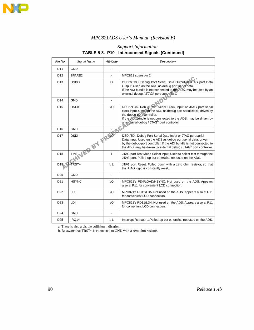
MPC821ADS User’s Manual (Revision B)
90
Release 1.4b
Support Information
a. There is also a visible collision indication.b. Be aware that TRST~ is connected to GND with a zero ohm resistor.
D11 GND -
D12 SPARE2 - MPC821 spare pin 2.
D13 DSDO O DSDO/TDO. Debug Port Serial Data Output or JTAG port DataOutput. Used on the ADS as debug port serial data. If the ADI bundle is not connected to the ADS, may be used by anexternal debug / JTAG
b
port controllers.
D14 GND -
D15 DSCK I/O DSCK/TCK. Debug Port Serial Clock input or JTAG port serialclock input. Used on the ADS as debug port serial clock, driven bythe debug-port controller. If the ADI bundle is not connected to the ADS, may be driven byan external debug / JTAG
b
port controller.
D16 GND -
D17 DSDI I/O DSDI/TDI. Debug Port Serial Data Input or JTAG port serial Data Input. Used on the ADS as debug port serial data, driven by the debug-port controller. If the ADI bundle is not connected tothe ADS, may be driven by external debug / JTAG
b
port controller.
D18 TMS I JTAG port Test Mode Select input. Used to select test through theJTAG port. Pulled-up but otherwise not used on the ADS.
D19 TRST~ I, L JTAG port Reset. Pulled down with a zero ohm resistor, so thatthe JTAG logic is constantly reset.
D20 GND -
D21 HSYNC I/O MPC821’s PD4/LOAD/HSYNC. Not used on the ADS. Appearsalso at P11 for convenient LCD connection.
D22 LD5 I/O MPC821’s PD12/LD5. Not used on the ADS. Appears also at P11for convenient LCD connection.
D23 LD4 I/O MPC821’s PD11/LD4. Not used on the ADS. Appears also at P11for convenient LCD connection.
D24 GND -
D25 IRQ1~ I, L Interrupt Request 1.Pulled-up but otherwise not used on the ADS.
TABLE 5-8. P10 - Interconnect Signals (Continued)
Pin No. Signal Name Attribute Description
ARCHIVED BY FREESCALE SEMICONDUCTOR, INC.
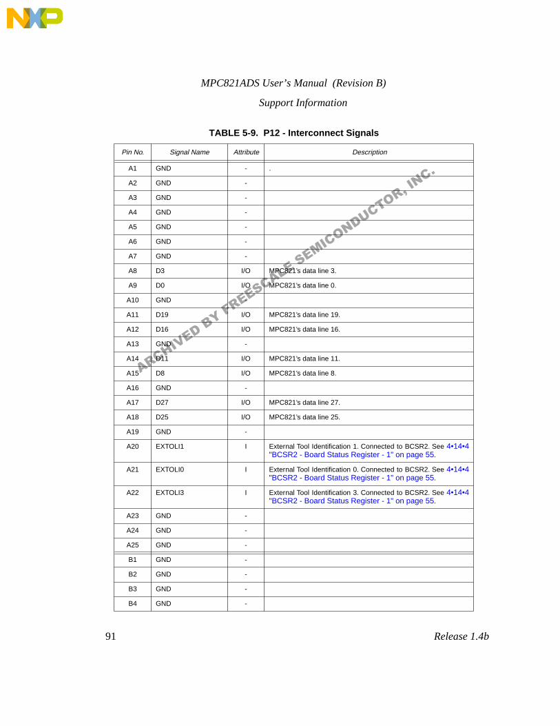
MPC821ADS User’s Manual (Revision B)
91
Release 1.4b
Support Information
TABLE 5-9. P12 - Interconnect Signals
Pin No. Signal Name Attribute Description
A1 GND - .
A2 GND -
A3 GND -
A4 GND -
A5 GND -
A6 GND -
A7 GND -
A8 D3 I/O MPC821’s data line 3.
A9 D0 I/O MPC821’s data line 0.
A10 GND -
A11 D19 I/O MPC821’s data line 19.
A12 D16 I/O MPC821’s data line 16.
A13 GND -
A14 D11 I/O MPC821’s data line 11.
A15 D8 I/O MPC821’s data line 8.
A16 GND -
A17 D27 I/O MPC821’s data line 27.
A18 D25 I/O MPC821’s data line 25.
A19 GND -
A20 EXTOLI1 I External Tool Identification 1. Connected to BCSR2. See
4•14•4"BCSR2 - Board Status Register - 1" on page 55
.
A21 EXTOLI0 I External Tool Identification 0. Connected to BCSR2. See
4•14•4"BCSR2 - Board Status Register - 1" on page 55
.
A22 EXTOLI3 I External Tool Identification 3. Connected to BCSR2. See
4•14•4"BCSR2 - Board Status Register - 1" on page 55
.
A23 GND -
A24 GND -
A25 GND -
B1 GND -
B2 GND -
B3 GND -
B4 GND -
ARCHIVED BY FREESCALE SEMICONDUCTOR, INC.
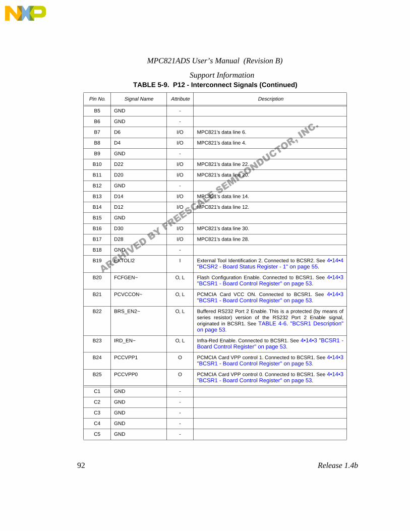
MPC821ADS User’s Manual (Revision B)
92
Release 1.4b
Support Information
B5 GND -
B6 GND -
B7 D6 I/O MPC821’s data line 6.
B8 D4 I/O MPC821’s data line 4.
B9 GND -
B10 D22 I/O MPC821’s data line 22.
B11 D20 I/O MPC821’s data line 20.
B12 GND -
B13 D14 I/O MPC821’s data line 14.
B14 D12 I/O MPC821’s data line 12.
B15 GND -
B16 D30 I/O MPC821’s data line 30.
B17 D28 I/O MPC821’s data line 28.
B18 GND -
B19 EXTOLI2 I External Tool Identification 2. Connected to BCSR2. See
4•14•4"BCSR2 - Board Status Register - 1" on page 55
.
B20 FCFGEN~ O, L Flash Configuration Enable. Connected to BCSR1. See
4•14•3"BCSR1 - Board Control Register" on page 53
.
B21 PCVCCON~ O, L PCMCIA Card VCC ON. Connected to BCSR1. See
4•14•3"BCSR1 - Board Control Register" on page 53
.
B22 BRS_EN2~ O, L Buffered RS232 Port 2 Enable. This is a protected (by means ofseries resistor) version of the RS232 Port 2 Enable signal,originated in BCSR1. See
TABLE 4-6. "BCSR1 Description"on page 53
.
B23 IRD_EN~ O, L Infra-Red Enable. Connected to BCSR1. See
4•14•3 "BCSR1 -Board Control Register" on page 53
.
B24 PCCVPP1 O PCMCIA Card VPP control 1. Connected to BCSR1. See
4•14•3"BCSR1 - Board Control Register" on page 53
.
B25 PCCVPP0 O PCMCIA Card VPP control 0. Connected to BCSR1. See
4•14•3"BCSR1 - Board Control Register" on page 53
.
C1 GND -
C2 GND -
C3 GND -
C4 GND -
C5 GND -
TABLE 5-9. P12 - Interconnect Signals (Continued)
Pin No. Signal Name Attribute Description
ARCHIVED BY FREESCALE SEMICONDUCTOR, INC.
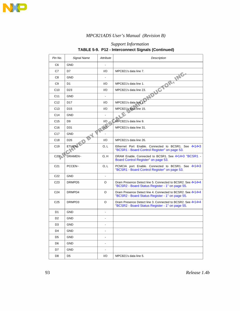
MPC821ADS User’s Manual (Revision B)
93
Release 1.4b
Support Information
C6 GND -
C7 D7 I/O MPC821’s data line 7.
C8 GND -
C9 D1 I/O MPC821’s data line 1.
C10 D23 I/O MPC821’s data line 23.
C11 GND -
C12 D17 I/O MPC821’s data line 17.
C13 D15 I/O MPC821’s data line 15.
C14 GND -
C15 D9 I/O MPC821’s data line 9.
C16 D31 I/O MPC821’s data line 31.
C17 GND -
C18 D26 I/O MPC821’s data line 26.
C19 ETHEN~ O, L Ethernet Port Enable. Connected to BCSR1. See
4•14•3"BCSR1 - Board Control Register" on page 53
.
C20 DRAMEN~ O, H DRAM Enable. Connected to BCSR1. See 4•14•3 "BCSR1 -Board Control Register" on page 53.
C21 PCCEN~ O, L PCMCIA port Enable. Connected to BCSR1. See 4•14•3"BCSR1 - Board Control Register" on page 53.
C22 GND -
C23 DRMPD5 O Dram Presence Detect line 5. Connected to BCSR2. See 4•14•4"BCSR2 - Board Status Register - 1" on page 55.
C24 DRMPD4 O Dram Presence Detect line 4. Connected to BCSR2. See 4•14•4"BCSR2 - Board Status Register - 1" on page 55.
C25 DRMPD3 O Dram Presence Detect line 3. Connected to BCSR2. See 4•14•4"BCSR2 - Board Status Register - 1" on page 55.
D1 GND -
D2 GND -
D3 GND -
D4 GND -
D5 GND -
D6 GND -
D7 GND -
D8 D5 I/O MPC821’s data line 5.
TABLE 5-9. P12 - Interconnect Signals (Continued)
Pin No. Signal Name Attribute Description
ARCHIVED BY FREESCALE SEMICONDUCTOR, INC.
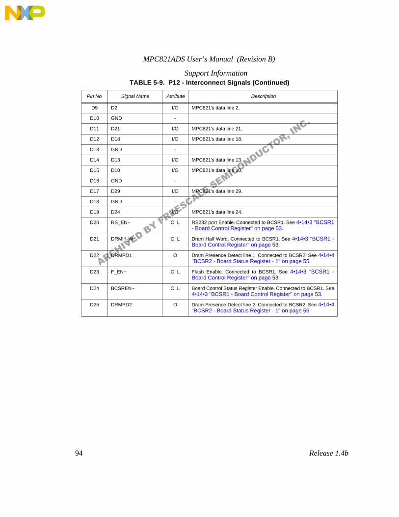
MPC821ADS User’s Manual (Revision B)
94 Release 1.4b
Support Information
D9 D2 I/O MPC821’s data line 2.
D10 GND -
D11 D21 I/O MPC821’s data line 21.
D12 D18 I/O MPC821’s data line 18.
D13 GND -
D14 D13 I/O MPC821’s data line 13.
D15 D10 I/O MPC821’s data line 10.
D16 GND -
D17 D29 I/O MPC821’s data line 29.
D18 GND -
D19 D24 I/O MPC821’s data line 24.
D20 RS_EN~ O, L RS232 port Enable. Connected to BCSR1. See 4•14•3 "BCSR1- Board Control Register" on page 53.
D21 DRMH_W~ O, L Dram Half Word. Connected to BCSR1. See 4•14•3 "BCSR1 -Board Control Register" on page 53.
D22 DRMPD1 O Dram Presence Detect line 1. Connected to BCSR2. See 4•14•4"BCSR2 - Board Status Register - 1" on page 55.
D23 F_EN~ O, L Flash Enable. Connected to BCSR1. See 4•14•3 "BCSR1 -Board Control Register" on page 53.
D24 BCSREN~ O, L Board Control Status Register Enable. Connected to BCSR1. See4•14•3 "BCSR1 - Board Control Register" on page 53.
D25 DRMPD2 O Dram Presence Detect line 2. Connected to BCSR2. See 4•14•4"BCSR2 - Board Status Register - 1" on page 55.
TABLE 5-9. P12 - Interconnect Signals (Continued)
Pin No. Signal Name Attribute Description
ARCHIVED BY FREESCALE SEMICONDUCTOR, INC.
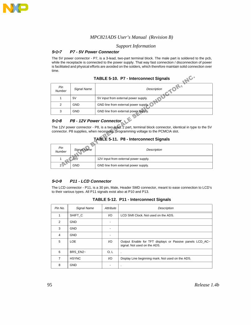
MPC821ADS User’s Manual (Revision B)
95 Release 1.4b
Support Information5•1•7 P7 - 5V Power ConnectorThe 5V power connector - P7, is a 3-lead, two-part terminal block. The male part is soldered to the pcb,while the receptacle is connected to the power supply. That way fast connection / disconnection of poweris facilitated and physical efforts are avoided on the solders, which therefore maintain solid connection overtime.
5•1•8 P8 - 12V Power ConnectorThe 12V power connector - P8, is a two-lead, 2 part, terminal block connector, identical in type to the 5Vconnector. P8 supplies, when necessary, programming voltage to the PCMCIA slot.
5•1•9 P11 - LCD ConnectorThe LCD connector - P11, is a 30 pin, Male, Header SMD connector, meant to ease connection to LCD’sto their various types. All P11 signals exist also at P10 and P13.
TABLE 5-10. P7 - Interconnect Signals
Pin Number
Signal Name Description
1 5V 5V input from external power supply.
2 GND GND line from external power supply.
3 GND GND line from external power supply.
TABLE 5-11. P8 - Interconnect Signals
Pin Number
Signal Name Description
1 12V 12V input from external power supply.
2 GND GND line from external power supply.
TABLE 5-12. P11 - Interconnect Signals
Pin No. Signal Name Attribute Description
1 SHIFT_C I/O LCD Shift Clock. Not used on the ADS.
2 GND -
3 GND -
4 GND -
5 LOE I/O Output Enable for TFT displays or Passive panels LCD_AC~signal. Not used on the ADS.
6 BRS_EN2~ O, L .
7 HSYNC I/O Display Line beginning mark. Not used on the ADS.
8 GND - .
ARCHIVED BY FREESCALE SEMICONDUCTOR, INC.
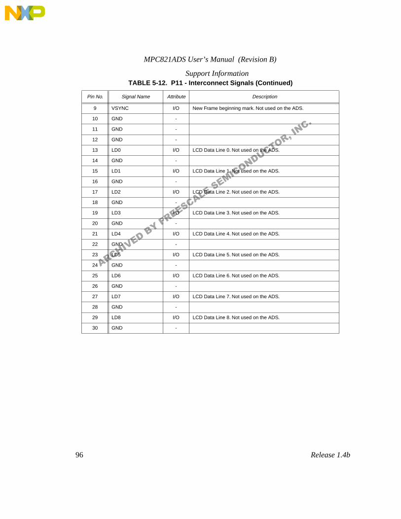
MPC821ADS User’s Manual (Revision B)
96 Release 1.4b
Support Information
9 VSYNC I/O New Frame beginning mark. Not used on the ADS.
10 GND -
11 GND -
12 GND -
13 LD0 I/O LCD Data Line 0. Not used on the ADS.
14 GND -
15 LD1 I/O LCD Data Line 1. Not used on the ADS.
16 GND -
17 LD2 I/O LCD Data Line 2. Not used on the ADS.
18 GND -
19 LD3 I/O LCD Data Line 3. Not used on the ADS.
20 GND -
21 LD4 I/O LCD Data Line 4. Not used on the ADS.
22 GND -
23 LD5 I/O LCD Data Line 5. Not used on the ADS.
24 GND -
25 LD6 I/O LCD Data Line 6. Not used on the ADS.
26 GND -
27 LD7 I/O LCD Data Line 7. Not used on the ADS.
28 GND -
29 LD8 I/O LCD Data Line 8. Not used on the ADS.
30 GND -
TABLE 5-12. P11 - Interconnect Signals (Continued)
Pin No. Signal Name Attribute Description
ARCHIVED BY FREESCALE SEMICONDUCTOR, INC.
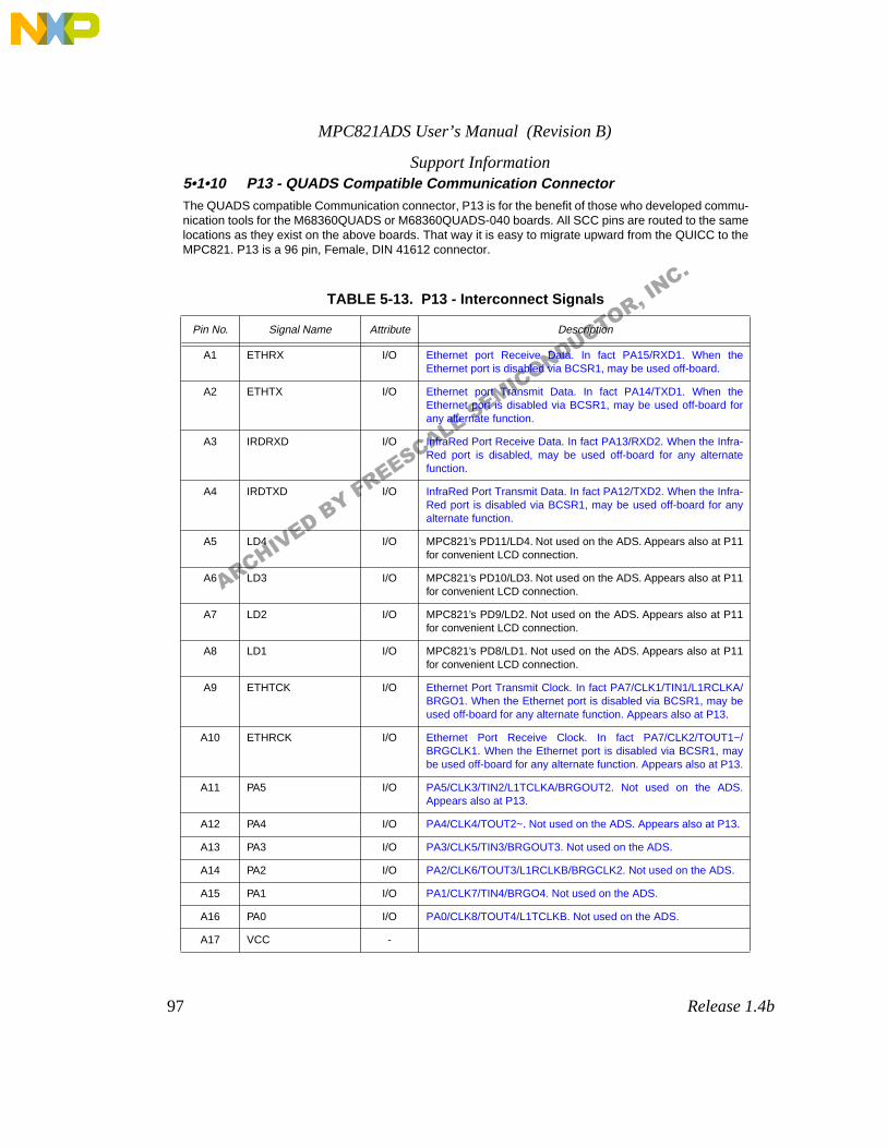
MPC821ADS User’s Manual (Revision B)
97 Release 1.4b
Support Information5•1•10 P13 - QUADS Compatible Communication ConnectorThe QUADS compatible Communication connector, P13 is for the benefit of those who developed commu-nication tools for the M68360QUADS or M68360QUADS-040 boards. All SCC pins are routed to the samelocations as they exist on the above boards. That way it is easy to migrate upward from the QUICC to theMPC821. P13 is a 96 pin, Female, DIN 41612 connector.
TABLE 5-13. P13 - Interconnect Signals
Pin No. Signal Name Attribute Description
A1 ETHRX I/O Ethernet port Receive Data. In fact PA15/RXD1. When theEthernet port is disabled via BCSR1, may be used off-board.
A2 ETHTX I/O Ethernet port Transmit Data. In fact PA14/TXD1. When theEthernet port is disabled via BCSR1, may be used off-board forany alternate function.
A3 IRDRXD I/O InfraRed Port Receive Data. In fact PA13/RXD2. When the Infra-Red port is disabled, may be used off-board for any alternatefunction.
A4 IRDTXD I/O InfraRed Port Transmit Data. In fact PA12/TXD2. When the Infra-Red port is disabled via BCSR1, may be used off-board for anyalternate function.
A5 LD4 I/O MPC821’s PD11/LD4. Not used on the ADS. Appears also at P11for convenient LCD connection.
A6 LD3 I/O MPC821’s PD10/LD3. Not used on the ADS. Appears also at P11for convenient LCD connection.
A7 LD2 I/O MPC821’s PD9/LD2. Not used on the ADS. Appears also at P11for convenient LCD connection.
A8 LD1 I/O MPC821’s PD8/LD1. Not used on the ADS. Appears also at P11for convenient LCD connection.
A9 ETHTCK I/O Ethernet Port Transmit Clock. In fact PA7/CLK1/TIN1/L1RCLKA/BRGO1. When the Ethernet port is disabled via BCSR1, may beused off-board for any alternate function. Appears also at P13.
A10 ETHRCK I/O Ethernet Port Receive Clock. In fact PA7/CLK2/TOUT1~/BRGCLK1. When the Ethernet port is disabled via BCSR1, maybe used off-board for any alternate function. Appears also at P13.
A11 PA5 I/O PA5/CLK3/TIN2/L1TCLKA/BRGOUT2. Not used on the ADS.Appears also at P13.
A12 PA4 I/O PA4/CLK4/TOUT2~. Not used on the ADS. Appears also at P13.
A13 PA3 I/O PA3/CLK5/TIN3/BRGOUT3. Not used on the ADS.
A14 PA2 I/O PA2/CLK6/TOUT3/L1RCLKB/BRGCLK2. Not used on the ADS.
A15 PA1 I/O PA1/CLK7/TIN4/BRGO4. Not used on the ADS.
A16 PA0 I/O PA0/CLK8/TOUT4/L1TCLKB. Not used on the ADS.
A17 VCC -
ARCHIVED BY FREESCALE SEMICONDUCTOR, INC.
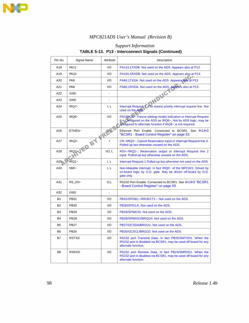
MPC821ADS User’s Manual (Revision B)
98 Release 1.4b
Support Information
A18 PA11 I/O PA11/L1TXDB. Not used on the ADS. Appears also at P13.
A19 PA10 I/O PA10/L1RXDB. Not used on the ADS. Appears also at P13.
A20 PA9 I/O PA9/L1TXDA. Not used on the ADS. Appears also at P13.
A21 PA8 I/O PA8/L1RXDA. Not used on the ADS. Appears also at P13.
A22 GND -
A23 GND -
A24 IRQ7~ I, L Interrupt Request 7. The lowest priority interrupt request line. Notused on the ADS.
A25 IRQ6~ I/O FRZ/IRQ6~. Freeze (debug-mode) indication or Interrupt Request6~. Configured on the ADS as IRQ6~. Not by ADS logic, may beconfigured to alternate function if IRQ6~ is not required.
A26 ETHEN~ O, L Ethernet Port Enable. Connected to BCSR1. See 4•14•3"BCSR1 - Board Control Register" on page 53.
A27 IRQ3~ I CR~/IRQ3~. Cancel Reservation input or Interrupt Request line 3.Pulled-up but otherwise unused on the ADS.
A28 IRQ2~ I/O, L RSV~/IRQ2~. Reservation output or Interrupt Request line 2input. Pulled-up but otherwise unused on the ADS.
A29 IRQ1~ I, L Interrupt Request 1.Pulled-up but otherwise not used on the ADS.
A30 NMI~ I, L Non-Makable Interrupt. In fact IRQ0~ of the MPC821. Driven byon-board logic by O.D. gate. May be driven off-board by O.D.gate only.
A31 RS_EN~ O,L RS232 Port Enable. Connected to BCSR1. See 4•14•3 "BCSR1- Board Control Register" on page 53.
A32 GND -
B1 PB31 I/O PB31/SPISEL~/RRJECT1~. Not used on the ADS.
B2 PB30 I/O PB30/SPICLK. Not used on the ADS.
B3 PB29 I/O PB29/SPIMOSI. Not used on the ADS.
B4 PB28 I/O PB28/SPIMISO/BRGO4. Not used on the ADS.
B5 PB27 I/O PB27/I2CSDA/BRGO1. Not used on the ADS.
B6 PB26 I/O PB26/I2CSCL/BRGO2. Not used on the ADS.
B7 RSTXD I/O RS232 port Transmit Data. In fact PB25/SMTXD1. When theRS232 port is disabled via BCSR1, may be used off-board for anyalternate function.
B8 RSRXD I/O RS232 port Receive Data. In fact PB24/SMRXD1. When theRS232 port is disabled via BCSR1, may be used off-board for anyalternate function.
TABLE 5-13. P13 - Interconnect Signals (Continued)
Pin No. Signal Name Attribute Description
ARCHIVED BY FREESCALE SEMICONDUCTOR, INC.
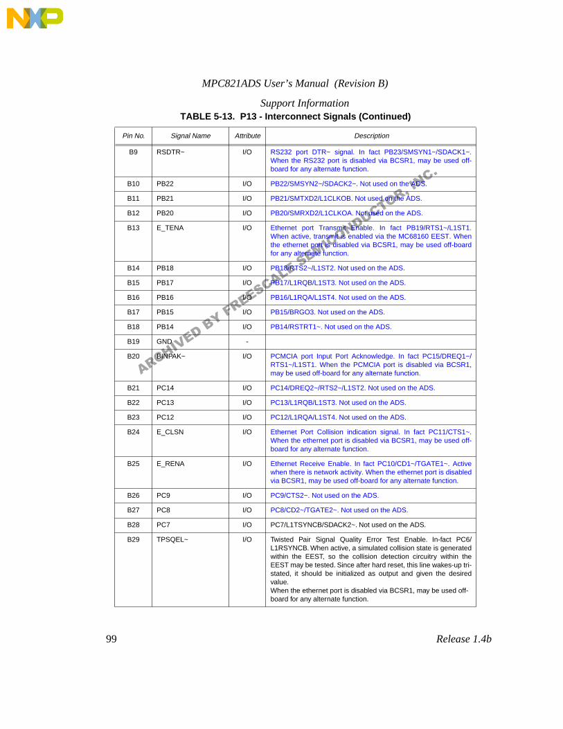
MPC821ADS User’s Manual (Revision B)
99 Release 1.4b
Support Information
B9 RSDTR~ I/O RS232 port DTR~ signal. In fact PB23/SMSYN1~/SDACK1~.When the RS232 port is disabled via BCSR1, may be used off-board for any alternate function.
B10 PB22 I/O PB22/SMSYN2~/SDACK2~. Not used on the ADS.
B11 PB21 I/O PB21/SMTXD2/L1CLKOB. Not used on the ADS.
B12 PB20 I/O PB20/SMRXD2/L1CLKOA. Not used on the ADS.
B13 E_TENA I/O Ethernet port Transmit Enable. In fact PB19/RTS1~/L1ST1.When active, transmit is enabled via the MC68160 EEST. Whenthe ethernet port is disabled via BCSR1, may be used off-boardfor any alternate function.
B14 PB18 I/O PB18/RTS2~/L1ST2. Not used on the ADS.
B15 PB17 I/O PB17/L1RQB/L1ST3. Not used on the ADS.
B16 PB16 I/O PB16/L1RQA/L1ST4. Not used on the ADS.
B17 PB15 I/O PB15/BRGO3. Not used on the ADS.
B18 PB14 I/O PB14/RSTRT1~. Not used on the ADS.
B19 GND -
B20 BINPAK~ I/O PCMCIA port Input Port Acknowledge. In fact PC15/DREQ1~/RTS1~/L1ST1. When the PCMCIA port is disabled via BCSR1,may be used off-board for any alternate function.
B21 PC14 I/O PC14/DREQ2~/RTS2~/L1ST2. Not used on the ADS.
B22 PC13 I/O PC13/L1RQB/L1ST3. Not used on the ADS.
B23 PC12 I/O PC12/L1RQA/L1ST4. Not used on the ADS.
B24 E_CLSN I/O Ethernet Port Collision indication signal. In fact PC11/CTS1~.When the ethernet port is disabled via BCSR1, may be used off-board for any alternate function.
B25 E_RENA I/O Ethernet Receive Enable. In fact PC10/CD1~/TGATE1~. Activewhen there is network activity. When the ethernet port is disabledvia BCSR1, may be used off-board for any alternate function.
B26 PC9 I/O PC9/CTS2~. Not used on the ADS.
B27 PC8 I/O PC8/CD2~/TGATE2~. Not used on the ADS.
B28 PC7 I/O PC7/L1TSYNCB/SDACK2~. Not used on the ADS.
B29 TPSQEL~ I/O Twisted Pair Signal Quality Error Test Enable. In-fact PC6/L1RSYNCB. When active, a simulated collision state is generatedwithin the EEST, so the collision detection circuitry within theEEST may be tested. Since after hard reset, this line wakes-up tri-stated, it should be initialized as output and given the desiredvalue. When the ethernet port is disabled via BCSR1, may be used off-board for any alternate function.
TABLE 5-13. P13 - Interconnect Signals (Continued)
Pin No. Signal Name Attribute Description
ARCHIVED BY FREESCALE SEMICONDUCTOR, INC.
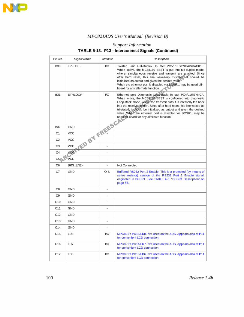
MPC821ADS User’s Manual (Revision B)
100 Release 1.4b
Support Information
B30 TPFLDL~ I/O Twisted Pair Full-Duplex. In fact PC5/L1TSYNCA/SDACK1~.When active, the MC68160 EEST is put into full-duplex mode,where, simultaneous receive and transmit are enabled. Sinceafter hard reset, this line wakes-up tri-stated, it should beinitialized as output and given the desired value. When the ethernet port is disabled via BCSR1, may be used off-board for any alternate function.
B31 ETHLOOP I/O Ethernet port Diagnostic Loop-Back. In fact PC4/L1RSYNCA.When active, the MC68160 EEST is configured into diagnosticLoop-Back mode, where the transmit output is internally fed backinto the receive section. Since after hard reset, this line wakes-uptri-stated, it should be initialized as output and given the desiredvalue. When the ethernet port is disabled via BCSR1, may beused off-board for any alternate function.
B32 GND -
C1 VCC -
C2 VCC -
C3 VCC -
C4 VCC -
C5 VCC -
C6 BRS_EN2~ - Not Connected
C7 GND O, L Buffered RS232 Port 2 Enable. This is a protected (by means ofseries resistor) version of the RS232 Port 2 Enable signal,originated in BCSR1. See TABLE 4-6. "BCSR1 Description" onpage 53.
C8 GND -
C9 GND -
C10 GND -
C11 GND -
C12 GND -
C13 GND -
C14 GND -
C15 LD8 I/O MPC821’s PD15/LD8. Not used on the ADS. Appears also at P11for convenient LCD connection.
C16 LD7 I/O MPC821’s PD14/LD7. Not used on the ADS. Appears also at P11for convenient LCD connection.
C17 LD6 I/O MPC821’s PD13/LD6. Not used on the ADS. Appears also at P11for convenient LCD connection.
TABLE 5-13. P13 - Interconnect Signals (Continued)
Pin No. Signal Name Attribute Description
ARCHIVED BY FREESCALE SEMICONDUCTOR, INC.
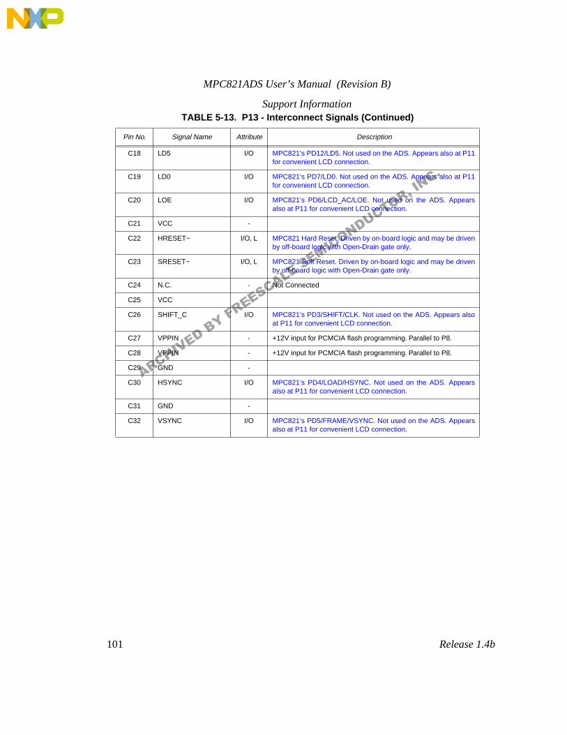
MPC821ADS User’s Manual (Revision B)
101 Release 1.4b
Support Information
C18 LD5 I/O MPC821’s PD12/LD5. Not used on the ADS. Appears also at P11for convenient LCD connection.
C19 LD0 I/O MPC821’s PD7/LD0. Not used on the ADS. Appears also at P11for convenient LCD connection.
C20 LOE I/O MPC821’s PD6/LCD_AC/LOE. Not used on the ADS. Appearsalso at P11 for convenient LCD connection.
C21 VCC -
C22 HRESET~ I/O, L MPC821 Hard Reset. Driven by on-board logic and may be drivenby off-board logic with Open-Drain gate only.
C23 SRESET~ I/O, L MPC821 Soft Reset. Driven by on-board logic and may be drivenby off-board logic with Open-Drain gate only.
C24 N.C. - Not Connected
C25 VCC -
C26 SHIFT_C I/O MPC821’s PD3/SHIFT/CLK. Not used on the ADS. Appears alsoat P11 for convenient LCD connection.
C27 VPPIN - +12V input for PCMCIA flash programming. Parallel to P8.
C28 VPPIN - +12V input for PCMCIA flash programming. Parallel to P8.
C29 GND -
C30 HSYNC I/O MPC821’s PD4/LOAD/HSYNC. Not used on the ADS. Appearsalso at P11 for convenient LCD connection.
C31 GND -
C32 VSYNC I/O MPC821’s PD5/FRAME/VSYNC. Not used on the ADS. Appearsalso at P11 for convenient LCD connection.
TABLE 5-13. P13 - Interconnect Signals (Continued)
Pin No. Signal Name Attribute Description
ARCHIVED BY FREESCALE SEMICONDUCTOR, INC.
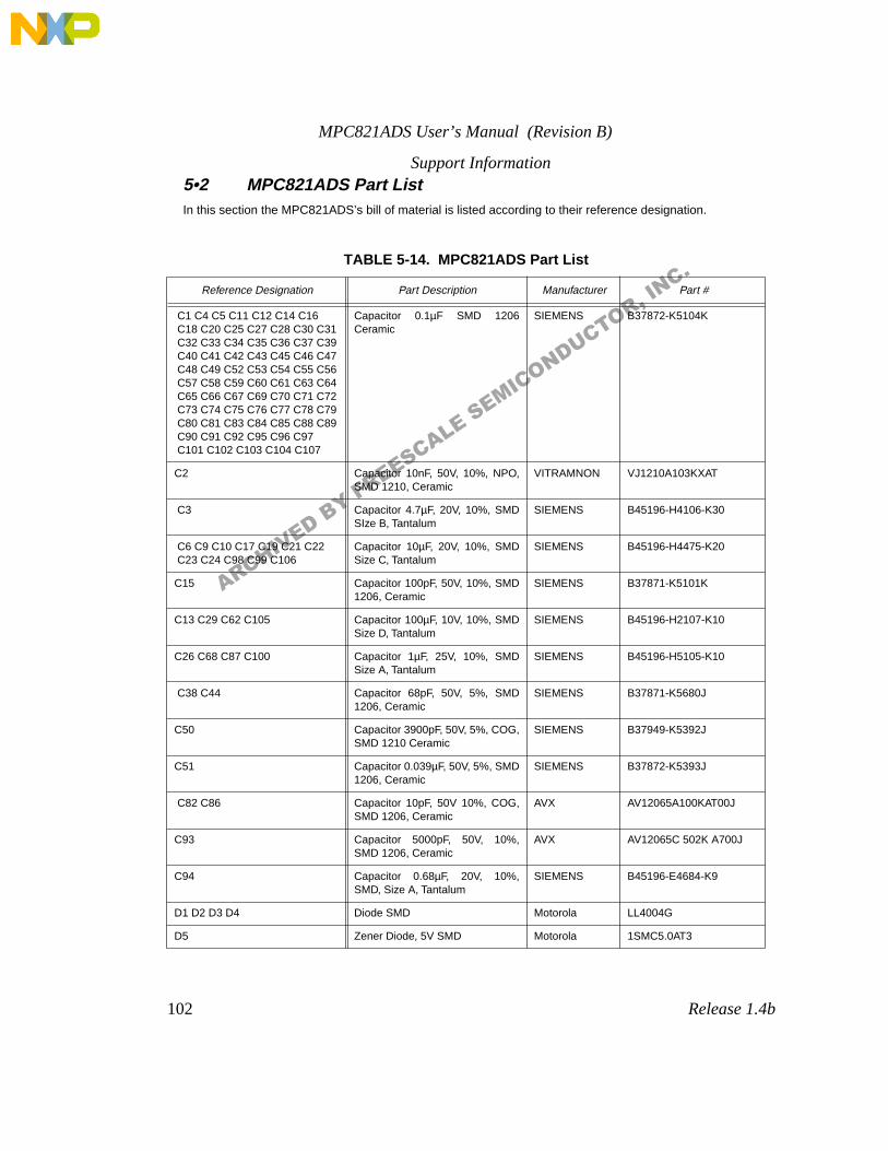
MPC821ADS User’s Manual (Revision B)
102 Release 1.4b
Support Information5•2 MPC821ADS Part ListIn this section the MPC821ADS’s bill of material is listed according to their reference designation.
TABLE 5-14. MPC821ADS Part List
Reference Designation Part Description Manufacturer Part #
C1 C4 C5 C11 C12 C14 C16 C18 C20 C25 C27 C28 C30 C31 C32 C33 C34 C35 C36 C37 C39 C40 C41 C42 C43 C45 C46 C47 C48 C49 C52 C53 C54 C55 C56 C57 C58 C59 C60 C61 C63 C64 C65 C66 C67 C69 C70 C71 C72 C73 C74 C75 C76 C77 C78 C79 C80 C81 C83 C84 C85 C88 C89 C90 C91 C92 C95 C96 C97 C101 C102 C103 C104 C107
Capacitor 0.1µF SMD 1206Ceramic
SIEMENS B37872-K5104K
C2 Capacitor 10nF, 50V, 10%, NPO,SMD 1210, Ceramic
VITRAMNON VJ1210A103KXAT
C3 Capacitor 4.7µF, 20V, 10%, SMDSIze B, Tantalum
SIEMENS B45196-H4106-K30
C6 C9 C10 C17 C19 C21 C22 C23 C24 C98 C99 C106
Capacitor 10µF, 20V, 10%, SMDSize C, Tantalum
SIEMENS B45196-H4475-K20
C15 Capacitor 100pF, 50V, 10%, SMD1206, Ceramic
SIEMENS B37871-K5101K
C13 C29 C62 C105 Capacitor 100µF, 10V, 10%, SMDSize D, Tantalum
SIEMENS B45196-H2107-K10
C26 C68 C87 C100 Capacitor 1µF, 25V, 10%, SMDSize A, Tantalum
SIEMENS B45196-H5105-K10
C38 C44 Capacitor 68pF, 50V, 5%, SMD1206, Ceramic
SIEMENS B37871-K5680J
C50 Capacitor 3900pF, 50V, 5%, COG,SMD 1210 Ceramic
SIEMENS B37949-K5392J
C51 Capacitor 0.039µF, 50V, 5%, SMD1206, Ceramic
SIEMENS B37872-K5393J
C82 C86 Capacitor 10pF, 50V 10%, COG,SMD 1206, Ceramic
AVX AV12065A100KAT00J
C93 Capacitor 5000pF, 50V, 10%,SMD 1206, Ceramic
AVX AV12065C 502K A700J
C94 Capacitor 0.68µF, 20V, 10%,SMD, Size A, Tantalum
SIEMENS B45196-E4684-K9
D1 D2 D3 D4 Diode SMD Motorola LL4004G
D5 Zener Diode, 5V SMD Motorola 1SMC5.0AT3
ARCHIVED BY FREESCALE SEMICONDUCTOR, INC.
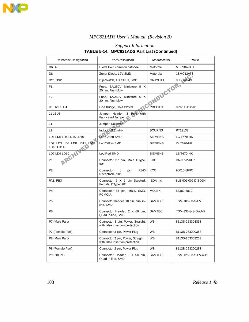
MPC821ADS User’s Manual (Revision B)
103 Release 1.4b
Support Information
D6 D7 Diode Pair, common cathode Motorola MBRD620CT
D8 Zener Diode, 12V SMD Motorola 1SMC12AT3
DS1 DS2 Dip-Switch, 4 X SPST, SMD GRAYHILL 90HBW04S
F1 Fuse, 5A/250V Miniature 5 X20mm, Fast-blow
F2 Fuse, 1A/250V Miniature 5 X20mm, Fast-blow
H1 H2 H3 H4 Gnd Bridge, Gold Plated PRECIDIP 999-11-112-10
J1 J2 J3 Jumper Header, 3 Pole withFabricated Jumper
J4 Jumper, Soldered.
L1 Inductor 8.2 mHy BOURNS PT12133
LD1 LD5 LD6 LD15 LD16 Led Green SMD SIEMENS LG T670-HK
LD2 LD3 LD4 LD8 LD11 LD12LD13 LD14
Led Yellow SMD SIEMENS LY T670-HK
LD7 LD9 LD10 Led Red SMD SIEMENS LS T670-HK
P1 Connector 37 pin, Male DType,90o
KCC DN-37-P-RCZ
P2 Connector 8 pin, RJ45Receptacle, 90o
KCC 90015-8P8C
PA3, PB3 Connector 2 X 9 pin Stacked,Female, DType, 90o
EDA Inc. 8LE 009 009 D 3 06H
P4 Connector 68 pin, Male, SMD,PCMCIA.
MOLEX 53380-6810
P5 Connector header, 10 pin, dual in-line, SMD
SAMTEC TSM-105-03-S-DV
P6 Connector Header, 2 X 60 pin,Quad In-line, SMD.
SAMTEC TSM-130-3-S-DV-A-P
P7 (Male Part) Connector 3 pin, Power, Straight,with false insertion protection.
WB 8113S-253303353
P7 (Female Part) Connector 3 pin, Power Plug WB 8113B-253200353
P8 (Male Part) Connector 2 pin, Power, Straight, with false insertion protection.
WB 8113S-253303253
P8 (Female Part) Connector 2 pin, Power Plug WB 8113B-253200253
P9 P10 P12 Connector Header 2 X 50 pin,Quad In-line, SMD
SAMTEC TSM-125-03-S-DV-A-P
TABLE 5-14. MPC821ADS Part List (Continued)
Reference Designation Part Description Manufacturer Part #
ARCHIVED BY FREESCALE SEMICONDUCTOR, INC.
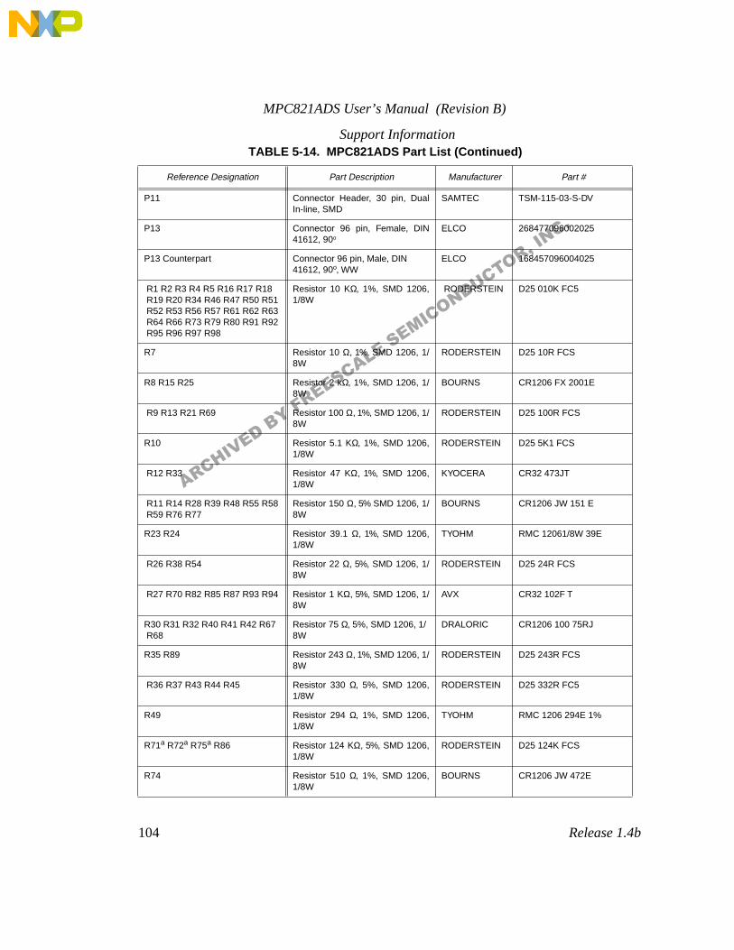
MPC821ADS User’s Manual (Revision B)
104 Release 1.4b
Support Information
P11 Connector Header, 30 pin, DualIn-line, SMD
SAMTEC TSM-115-03-S-DV
P13 Connector 96 pin, Female, DIN41612, 90o
ELCO 268477096002025
P13 Counterpart Connector 96 pin, Male, DIN 41612, 90o, WW
ELCO 168457096004025
R1 R2 R3 R4 R5 R16 R17 R18 R19 R20 R34 R46 R47 R50 R51 R52 R53 R56 R57 R61 R62 R63 R64 R66 R73 R79 R80 R91 R92 R95 R96 R97 R98
Resistor 10 KΩ, 1%, SMD 1206,1/8W
RODERSTEIN D25 010K FC5
R7 Resistor 10 Ω, 1%, SMD 1206, 1/8W
RODERSTEIN D25 10R FCS
R8 R15 R25 Resistor 2 kΩ, 1%, SMD 1206, 1/8W
BOURNS CR1206 FX 2001E
R9 R13 R21 R69 Resistor 100 Ω, 1%, SMD 1206, 1/8W
RODERSTEIN D25 100R FCS
R10 Resistor 5.1 KΩ, 1%, SMD 1206,1/8W
RODERSTEIN D25 5K1 FCS
R12 R33 Resistor 47 KΩ, 1%, SMD 1206,1/8W
KYOCERA CR32 473JT
R11 R14 R28 R39 R48 R55 R58 R59 R76 R77
Resistor 150 Ω, 5% SMD 1206, 1/8W
BOURNS CR1206 JW 151 E
R23 R24 Resistor 39.1 Ω, 1%, SMD 1206,1/8W
TYOHM RMC 12061/8W 39E
R26 R38 R54 Resistor 22 Ω, 5%, SMD 1206, 1/8W
RODERSTEIN D25 24R FCS
R27 R70 R82 R85 R87 R93 R94 Resistor 1 KΩ, 5%, SMD 1206, 1/8W
AVX CR32 102F T
R30 R31 R32 R40 R41 R42 R67 R68
Resistor 75 Ω, 5%, SMD 1206, 1/8W
DRALORIC CR1206 100 75RJ
R35 R89 Resistor 243 Ω, 1%, SMD 1206, 1/8W
RODERSTEIN D25 243R FCS
R36 R37 R43 R44 R45 Resistor 330 Ω, 5%, SMD 1206,1/8W
RODERSTEIN D25 332R FC5
R49 Resistor 294 Ω, 1%, SMD 1206,1/8W
TYOHM RMC 1206 294E 1%
R71a R72a R75a R86 Resistor 124 KΩ, 5%, SMD 1206,1/8W
RODERSTEIN D25 124K FCS
R74 Resistor 510 Ω, 1%, SMD 1206,1/8W
BOURNS CR1206 JW 472E
TABLE 5-14. MPC821ADS Part List (Continued)
Reference Designation Part Description Manufacturer Part #
ARCHIVED BY FREESCALE SEMICONDUCTOR, INC.
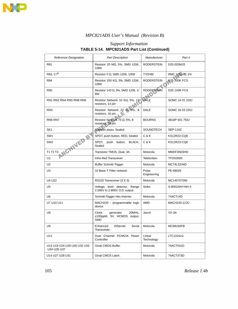
MPC821ADS User’s Manual (Revision B)
105 Release 1.4b
Support Information
R81 Resistor 20 MΩ, 5%, SMD 1206,1/8W
RODERSTEIN D25 020MJS
R83, C7b Resistor 0 Ω, SMD 1206, 1/8W TYOHM RMC 1206 0E 1%
R84 Resistor 200 KΩ, 5%, SMD 1206,1/8W
RODERSTEIN D25 200K FCS
R90 Resistor 143 Ω, 5%, SMD 1206, 1/8W
RODERSTEIN D25 143R FCS
RN1 RN2 RN4 RN5 RN8 RN9 Resistor Network 10 KΩ, 5%, 13resistors, 14 pin
DALE SOMC 14 01 103J
RN3 Resistor Network 22 Ω, 5%, 8resistors, 16 pin.
DALE SOMC 16 03 220J
RN6 RN7 Resistor Network 75 Ω, 5%, 8 resistors, 16 pin.
BOURNS 4816P 001 750J
SK1 Speaker piazo, Sealed SOUNDTECH SEP-1162
SW1 SPDT, push button, RED, Sealed C & K KS12R22-CQE
SW2 SPDT, push button, BLACK,Sealed
C & K KS12R23-CQE
T1 T2 T3 Transistor TMOS, Dual, 3A Motorola MMDF3N03HD
U1 Infra-Red Transceiver Telefunken TFDS3000
U2 Buffer Schmitt-Trigger Motorola MC74LS244D
U3 10 Base-T Filter network PulseEngineering
PE-68026
U4 U22 RS232 Transceiver (3 X 3) Motorola MC145707DW
U5 Voltage level detector. Range2.595V to 2.805V. O.D. output.
Seiko S-8052ANY-NH-X
U6 Schmitt-Trigger Hex Inverter. Motorola 74ACT14D
U7 U10 U11 MACH220 - programmable logicdevice
AMD MACH220-12JC
U8 Clock generator 20MHz,±100ppM, 5V, HCMOS output,SMD
Jauch VX-3A
U9 Enhanced Ethernet SerialTransceiver.
Motorola MC68160FB
U12 Dual Channel PCMCIA PowerController
LinearTechnology
LTC1315cG
U13 U19 U24 U29 U30 U32 U33 U34 U35 U37
Octal CMOS Buffer. Motorola 74ACT541D
U14 U27 U28 U31 Octal CMOS Latch. Motorola 74ACT373D
TABLE 5-14. MPC821ADS Part List (Continued)
Reference Designation Part Description Manufacturer Part #
ARCHIVED BY FREESCALE SEMICONDUCTOR, INC.
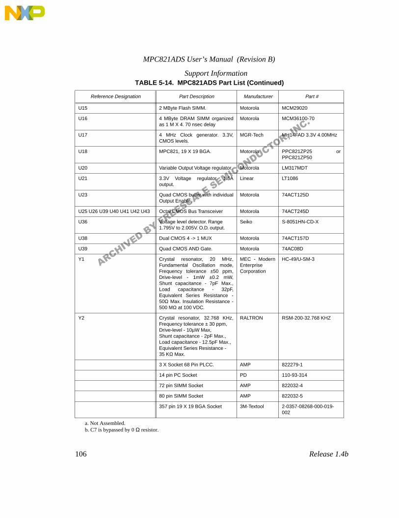
MPC821ADS User’s Manual (Revision B)
106 Release 1.4b
Support Information
a. Not Assembled.b. C7 is bypassed by 0 Ω resistor.
U15 2 MByte Flash SIMM. Motorola MCM29020
U16 4 MByte DRAM SIMM organizedas 1 M X 4. 70 nsec delay
Motorola MCM36100-70
U17 4 MHz Clock generator. 3.3V,CMOS levels.
MGR-Tech MH14FAD 3.3V 4.00MHz
U18 MPC821, 19 X 19 BGA. Motorola PPC821ZP25 orPPC821ZP50
U20 Variable Output Voltage regulator. Motorola LM317MDT
U21 3.3V Voltage regulator. 1.5Aoutput.
Linear LT1086
U23 Quad CMOS buffer with individualOutput Enable.
Motorola 74ACT125D
U25 U26 U39 U40 U41 U42 U43 Octal CMOS Bus Transceiver Motorola 74ACT245D
U36 Voltage level detector. Range 1.795V to 2.005V. O.D. output.
Seiko S-8051HN-CD-X
U38 Dual CMOS 4 -> 1 MUX Motorola 74ACT157D
U39 Quad CMOS AND Gate. Motorola 74AC08D
Y1 Crystal resonator, 20 MHz,Fundamental Oscillation mode,Frequency tolerance ±50 ppm,Drive-level - 1mW ±0.2 mW,Shunt capacitance - 7pF Max.,Load capacitance - 32pF,Equivalent Series Resistance -50Ω Max. Insulation Resistance -500 MΩ at 100 VDC.
MEC - ModernEnterpriseCorporation
HC-49/U-SM-3
Y2 Crystal resonator, 32.768 KHz,Frequency tolerance ± 30 ppm, Drive-level - 10µW Max, Shunt capacitance - 2pF Max., Load capacitance - 12.5pF Max., Equivalent Series Resistance - 35 KΩ Max.
RALTRON RSM-200-32.768 KHZ
3 X Socket 68 Pin PLCC. AMP 822279-1
14 pin PC Socket PD 110-93-314
72 pin SIMM Socket AMP 822032-4
80 pin SIMM Socket AMP 822032-5
357 pin 19 X 19 BGA Socket 3M-Textool 2-0357-08268-000-019-002
TABLE 5-14. MPC821ADS Part List (Continued)
Reference Designation Part Description Manufacturer Part #
ARCHIVED BY FREESCALE SEMICONDUCTOR, INC.
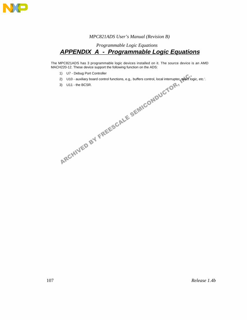
MPC821ADS User’s Manual (Revision B)
107
Release 1.4b
Programmable Logic Equations
APPENDIX A - Programmable Logic Equations
The MPC821ADS has 3 programmable logic devices installed on it. The source device is an AMDMACH220-12. These device support the following function on the ADS:
1) U7 - Debug Port Controller
2) U10 - auxiliary board control functions, e.g,. buffers control, local interrupter, reset logic, etc.’.
3) U11 - the BCSR.
ARCHIVED BY FREESCALE SEMICONDUCTOR, INC.
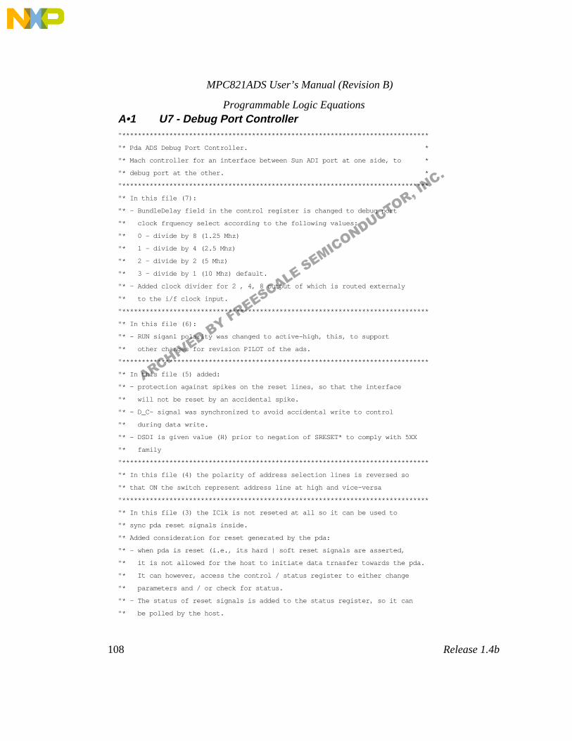
MPC821ADS User’s Manual (Revision B)
108
Release 1.4b
Programmable Logic Equations
A•1 U7 - Debug Port Controller
"******************************************************************************
"* Pda ADS Debug Port Controller. *
"* Mach controller for an interface between Sun ADI port at one side, to *
"* debug port at the other. *
"******************************************************************************
"* In this file (7):
"* - BundleDelay field in the control register is changed to debug port
"* clock frquency select according to the following values:
"* 0 - divide by 8 (1.25 Mhz)
"* 1 - divide by 4 (2.5 Mhz)
"* 2 - divide by 2 (5 Mhz)
"* 3 - divide by 1 (10 Mhz) default.
"* - Added clock divider for 2 , 4, 8 output of which is routed externaly
"* to the i/f clock input.
"******************************************************************************
"* In this file (6):
"* - RUN siganl polarity was changed to active-high, this, to support
"* other changes for revision PILOT of the ads.
"******************************************************************************
"* In this file (5) added:
"* - protection against spikes on the reset lines, so that the interface
"* will not be reset by an accidental spike.
"* - D_C~ signal was synchronized to avoid accidental write to control
"* during data write.
"* - DSDI is given value (H) prior to negation of SRESET* to comply with 5XX
"* family
"******************************************************************************
"* In this file (4) the polarity of address selection lines is reversed so
"* that ON the switch represent address line at high and vice-versa
"******************************************************************************
"* In this file (3) the IClk is not reseted at all so it can be used to
"* sync pda reset signals inside.
"* Added consideration for reset generated by the pda:
"* - when pda is reset (i.e., its hard | soft reset signals are asserted,
"* it is not allowed for the host to initiate data trnasfer towards the pda.
"* It can however, access the control / status register to either change
"* parameters and / or check for status.
"* - The status of reset signals is added to the status register, so it can
"* be polled by the host.
ARCHIVED BY FREESCALE SEMICONDUCTOR, INC.
MPC821ADS User’s Manual (Revision B)
109
Release 1.4b
Programmable Logic Equations
"******************************************************************************
module dbg_prt7
title 'MPC821ADS Debug Port Controller.
Originated for Ptec ADS, Shlomo Reches (MSIL) - October 26, 1993
Modified for Pda ADS, Yair Liebman - (MSIL) - April 04, 1995'
"******************************************************************************
"* Device declaration. *
"******************************************************************************
U07 device 'mach220a';
"******************************************************************************
"* ####### *
"* # # # ##### ###### ##### # # ## # #### *
"* # # # # # # # ## # # # # # *
"* ##### ## # ##### # # # # # # # # #### *
"* # ## # # ##### # # # ###### # # *
"* # # # # # # # # ## # # # # # *
"* ####### # # # ###### # # # # # # ###### #### *
"******************************************************************************
"******************************************************************************
"* Pins declaration. *
"******************************************************************************
"ADI Port pins.
HstReq PIN 20 ; "Host to ADS, write pulse. (IN)
AdsAck PIN 31 ISTYPE 'reg, buffer'; "ADS to host, write ack.
"(OUT,3s)
AdsReq PIN 2 ISTYPE 'reg, buffer'; "ADS to host, write
"signal. (OUT,3s)
HstAck PIN 54; "Host to ADS, write ack. (IN)
AdsHardReset PIN 50; "Host to ADS, Hard reset. (IN)
ARCHIVED BY FREESCALE SEMICONDUCTOR, INC.
MPC821ADS User’s Manual (Revision B)
110
Release 1.4b
Programmable Logic Equations
AdsSoftReset PIN 17; "Host to ADS, Soft reset. (IN)
HstEn~ PIN 3; "Host connected to ADS. (IN)
HostVcc PIN 49; "Host to ADS, host is on. (IN)
D_C~ PIN 51; "Host to ADS, select data
"or control access. (IN)
AdsSel0,
AdsSel1,
AdsSel2 PIN 22, 21, 9; "Host to ADS, card addr. (IN)
AdsAddr0,
AdsAddr1,
AdsAddr2 PIN 7, 6, 5; "ADS board address switch. (IN)
AdsSelect~ NODE ISTYPE 'com, buffer'; "ADS selection indicator. (OUT)
"******************************************************************************
"* PDA pins. Including debug port. *
"******************************************************************************
PdaHardReset~ PIN 40; "Pda's hard reset input. (I/O. o.d.)
PdaSoftReset~ PIN 65; "Pda's soft reset output. (I/O. o.d.)
VFLS0, VFLS1 PIN 10, 11; "Debug/Trap mode, report. (IN)
DSCK PIN 48 istype 'com'; "Pda's debug port clock. (Out)
DSDI PIN 47 istype 'com'; "Pda's debug serial data in (Out)
DSDO PIN 4; " Pda's debug serial data output (In)
"******************************************************************************
"* Mach to ADI data bus. *
"******************************************************************************
PD7,
PD6,
PD5,
PD4,
PD3,
PD2,
PD1,
ARCHIVED BY FREESCALE SEMICONDUCTOR, INC.
MPC821ADS User’s Manual (Revision B)
111
Release 1.4b
Programmable Logic Equations
PD0 PIN 66,60,67,59,58,57,56,55; "ADI data bus.(I/O)
"******************************************************************************
"* Clock gen pins. *
"******************************************************************************
DbgClk PIN 16; "Debug Clock input source. (IN)
DbgClkOut PIN 33 istype 'com' ; " to be connected to IClk. (out)
Clk2 PIN 14 istype 'reg, buffer'; "IClk divided by 2 (Out)
" (Out for testing, may be node)
IClk PIN 15; " Connected to Clkout externally (In)
"******************************************************************************
"* Misc.
"******************************************************************************
Run PIN 23 istype 'com'; "external indication
"******************************************************************************
"* ### *
"* # # # ##### ###### ##### # # ## # #### *
"* # ## # # # # # ## # # # # # *
"* # # # # # ##### # # # # # # # # #### *
"* # # # # # # ##### # # # ###### # # *
"* # # ## # # # # # ## # # # # # *
"* ### # # # ###### # # # # # # ###### #### *
"******************************************************************************
"******************************************************************************
"* Clock genrator Internals:
"******************************************************************************
DbgClkDivBy2NODE istype 'reg, buffer';
DbgClkDivBy4NODE istype 'reg, buffer';
DbgClkDivBy8NODE istype 'reg, buffer'; " counter (divider) signals.
Cstr0 NODE istype 'reg, buffer';
Cstr1 NODE istype 'reg, buffer'; " Clock Safe Transition Register
"******************************************************************************
"* Reset active. (Active when at least one of the reset sources is active) *
"******************************************************************************
PrimResetNODE istype 'com'; " Primary Reset. Host initiated
D_PrimResetNODE istype 'com'; " delayed Reset
ARCHIVED BY FREESCALE SEMICONDUCTOR, INC.
MPC821ADS User’s Manual (Revision B)
112
Release 1.4b
Programmable Logic Equations
DD_PrimReset NODE istype 'com'; " double delayed primary reset.
Reset NODE istype 'com'; " Interface reset.
PdaRst NODE istype 'reg, buffer'; " pda continued / initiated.
" part of the status register.
"******************************************************************************
"* ADS_ACK, ADS_REQ auxiliary internal control signals *
"******************************************************************************
S_HstReqNODE istype 'reg'; "sync. host req.
DS_HstReqNODE istype 'reg'; " double sync. host req.
S_D_C~ NODE istype 'reg, buffer'; " synchronized data/ control selection
S_HstAckNODE istype 'reg, buffer'; " sync host ack
DS_HstAckNODE istype 'reg, buffer'; " double sync host ack
BundleDelay1,
BundleDelay0NODE istype 'reg, buffer'; "delay counter for bundle
" delay compensation
BndTmrExpNODE istype 'com'; " terminal count for bundle
" delay timer.
PDOe NODE istype 'com'; "Mach to ADI data OE.
PdaHardResetEnNODE istype 'com'; " enables hard reset buffer.
PdaSoftResetEnNODE istype 'com'; " enables soft reset buffer.
"******************************************************************************
"* Tx Shift Register *
"******************************************************************************
TxReg7,
TxReg6,
TxReg5,
TxReg4,
TxReg3,
TxReg2,
TxReg1,
TxReg0 NODE istype 'reg, buffer'; " Transmit latch and
" shift register
"******************************************************************************
ARCHIVED BY FREESCALE SEMICONDUCTOR, INC.
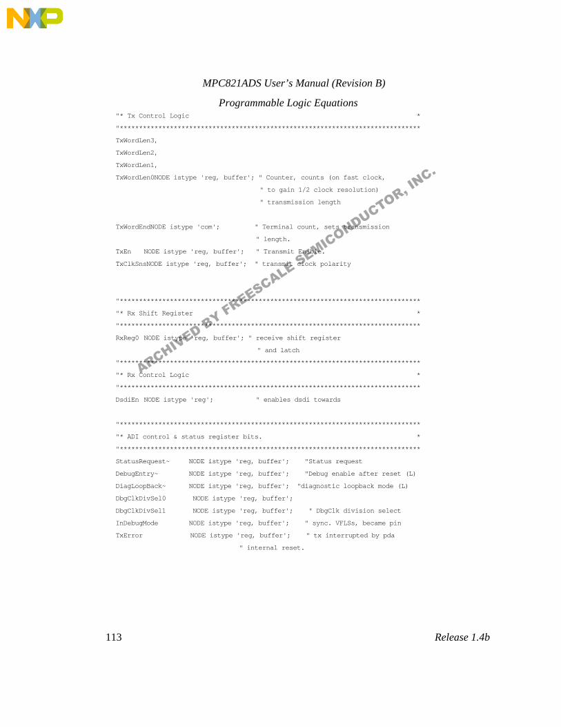
MPC821ADS User’s Manual (Revision B)
113
Release 1.4b
Programmable Logic Equations
"* Tx Control Logic *
"******************************************************************************
TxWordLen3,
TxWordLen2,
TxWordLen1,
TxWordLen0NODE istype 'reg, buffer'; " Counter, counts (on fast clock,
" to gain 1/2 clock resolution)
" transmission length
TxWordEndNODE istype 'com'; " Terminal count, sets transmission
" length.
TxEn NODE istype 'reg, buffer'; " Transmit Enable.
TxClkSnsNODE istype 'reg, buffer'; " transmit clock polarity
"******************************************************************************
"* Rx Shift Register *
"******************************************************************************
RxReg0 NODE istype 'reg, buffer'; " receive shift register
" and latch
"******************************************************************************
"* Rx Control Logic *
"******************************************************************************
DsdiEn NODE istype 'reg'; " enables dsdi towards
"******************************************************************************
"* ADI control & status register bits. *
"******************************************************************************
StatusRequest~ NODE istype 'reg, buffer'; "Status request
DebugEntry~ NODE istype 'reg, buffer'; "Debug enable after reset (L)
DiagLoopBack~ NODE istype 'reg, buffer'; "diagnostic loopback mode (L)
DbgClkDivSel0 NODE istype 'reg, buffer';
DbgClkDivSel1 NODE istype 'reg, buffer'; " DbgClk division select
InDebugMode NODE istype 'reg, buffer'; " sync. VFLSs, became pin
TxError NODE istype 'reg, buffer'; " tx interrupted by pda
" internal reset.
ARCHIVED BY FREESCALE SEMICONDUCTOR, INC.
MPC821ADS User’s Manual (Revision B)
114
Release 1.4b
Programmable Logic Equations
"******************************************************************************
"* ##### *
"* # # #### # # #### ##### ## # # ##### *
"* # # # ## # # # # # ## # # *
"* # # # # # # #### # # # # # # # *
"* # # # # # # # # ###### # # # # *
"* # # # # # ## # # # # # # ## # *
"* ##### #### # # #### # # # # # # *
"* *
"* ###### *
"* # # ###### #### # ## ##### *
"* # # # # # # # # # # *
"* # # ##### # # # # # # ##### *
"* # # # # # ###### ##### *
"* # # # # # # # # # # *
"* ###### ###### #### ###### # # # # *
"* *
"* ## ##### # #### # # *
"* # # # # # # ## # *
"* # # # # # # # # # *
"* ###### # # # # # # # *
"* # # # # # # # ## *
"* # # # # #### # # *
"******************************************************************************
H, L, X, Z = 1, 0, .X., .Z.;
C, D, U = .C., .D., .U.;
"******************************************************************************
"* Since all state machines operate at interface clock (IClk) there is no
"* need to have DbgClk driven during simulation (it will double the number
"* of vectors required). Therefore, an alternative clock generator was built
"* with which the 1/2 clock is the 1'st in the chain.
"* This alternative clock is compiled in if the SIMULATION variable is defined.
"* If not the original clock generator design is compiled, however simulation
"* will not pass then.
"******************************************************************************
"* SIMULATION = 1;
"******************************************************************************
ARCHIVED BY FREESCALE SEMICONDUCTOR, INC.
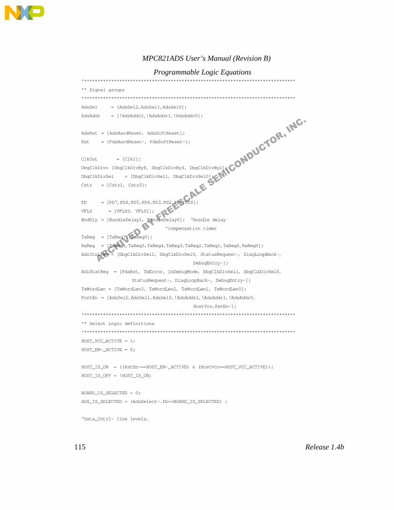
MPC821ADS User’s Manual (Revision B)
115
Release 1.4b
Programmable Logic Equations
"******************************************************************************
"* Signal groups
"******************************************************************************
AdsSel = [AdsSel2,AdsSel1,AdsSel0];
AdsAddr = [!AdsAddr2,!AdsAddr1,!AdsAddr0];
AdsRst = [AdsHardReset, AdsSoftReset];
Rst = [PdaHardReset~, PdaSoftReset~];
ClkOut = [Clk2];
DbgClkDiv= [DbgClkDivBy8, DbgClkDivBy4, DbgClkDivBy2];
DbgClkDivSel = [DbgClkDivSel1, DbgClkDivSel0];
Cstr = [Cstr1, Cstr0];
PD = [PD7,PD6,PD5,PD4,PD3,PD2,PD1,PD0];
VFLS = [VFLS0, VFLS1];
BndDly = [BundleDelay1, BundleDelay0]; "bundle delay
"compensation timer
TxReg = [TxReg7..TxReg0];
RxReg = [TxReg6,TxReg5,TxReg4,TxReg3,TxReg2,TxReg1,TxReg0,RxReg0];
AdiCtrlReg = [DbgClkDivSel1, DbgClkDivSel0, StatusRequest~, DiagLoopBack~,
DebugEntry~];
AdiStatReg = [PdaRst, TxError, InDebugMode, DbgClkDivSel1, DbgClkDivSel0,
StatusRequest~, DiagLoopBack~, DebugEntry~];
TxWordLen = [TxWordLen3, TxWordLen2, TxWordLen1, TxWordLen0];
PortEn = [AdsSel2,AdsSel1,AdsSel0,!AdsAddr2,!AdsAddr1,!AdsAddr0,
HostVcc,HstEn~];
"******************************************************************************
"* Select Logic definitions
"******************************************************************************
HOST_VCC_ACTIVE = 1;
HOST_EN~_ACTIVE = 0;
HOST_IS_ON = ((HstEn~==HOST_EN~_ACTIVE) & (HostVcc==HOST_VCC_ACTIVE));
HOST_IS_OFF = !HOST_IS_ON;
BOARD_IS_SELECTED = 0;
ADS_IS_SELECTED = (AdsSelect~.fb==BOARD_IS_SELECTED) ;
"Data_Cntrl~ line levels.
ARCHIVED BY FREESCALE SEMICONDUCTOR, INC.
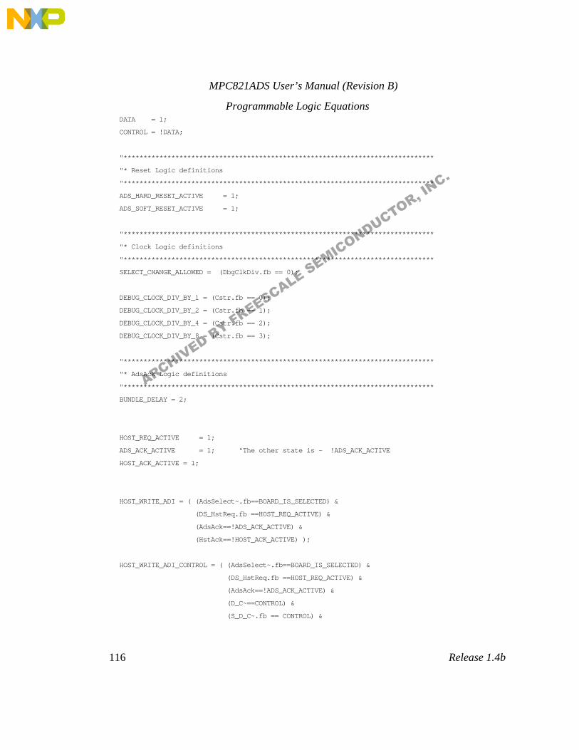
MPC821ADS User’s Manual (Revision B)
116
Release 1.4b
Programmable Logic Equations
DATA = 1;
CONTROL = !DATA;
"******************************************************************************
"* Reset Logic definitions
"******************************************************************************
ADS_HARD_RESET_ACTIVE = 1;
ADS_SOFT_RESET_ACTIVE = 1;
"******************************************************************************
"* Clock Logic definitions
"******************************************************************************
SELECT_CHANGE_ALLOWED = (DbgClkDiv.fb == 0);
DEBUG_CLOCK_DIV_BY_1 = (Cstr.fb == 0);
DEBUG_CLOCK_DIV_BY_2 = (Cstr.fb == 1);
DEBUG_CLOCK_DIV_BY_4 = (Cstr.fb == 2);
DEBUG_CLOCK_DIV_BY_8 = (Cstr.fb == 3);
"******************************************************************************
"* AdsAck Logic definitions
"******************************************************************************
BUNDLE_DELAY = 2;
HOST_REQ_ACTIVE = 1;
ADS_ACK_ACTIVE = 1; "The other state is - !ADS_ACK_ACTIVE
HOST_ACK_ACTIVE = 1;
HOST_WRITE_ADI = ( (AdsSelect~.fb==BOARD_IS_SELECTED) &
(DS_HstReq.fb ==HOST_REQ_ACTIVE) &
(AdsAck==!ADS_ACK_ACTIVE) &
(HstAck==!HOST_ACK_ACTIVE) );
HOST_WRITE_ADI_CONTROL = ( (AdsSelect~.fb==BOARD_IS_SELECTED) &
(DS_HstReq.fb ==HOST_REQ_ACTIVE) &
(AdsAck==!ADS_ACK_ACTIVE) &
(D_C~==CONTROL) &
(S_D_C~.fb == CONTROL) &
ARCHIVED BY FREESCALE SEMICONDUCTOR, INC.
MPC821ADS User’s Manual (Revision B)
117
Release 1.4b
Programmable Logic Equations
(HstAck==!HOST_ACK_ACTIVE) );
HOST_WRITE_ADI_DATA = ( (AdsSelect~.fb==BOARD_IS_SELECTED) &
(DS_HstReq.fb==HOST_REQ_ACTIVE) &
(AdsAck==!ADS_ACK_ACTIVE) &
(D_C~==DATA) &
(S_D_C~.fb ==DATA) &
(HstAck==!HOST_ACK_ACTIVE) );
HOST_WRITE_COMPLETE = ( (AdsSelect~.fb==BOARD_IS_SELECTED) &
(DS_HstReq.fb==!HOST_REQ_ACTIVE) &
(AdsAck==!ADS_ACK_ACTIVE) );
"******************************************************************************
"* Control & Status register definitions
"******************************************************************************
STATUS_REQUEST= 0;
DEBUG_ENTRY= 0;
DIAG_LOOP_BACK= 0;
IN_DEBUG_MODE = 1;
TX_DONE_OK= 0;
TX_INTERRUPTED = !TX_DONE_OK;
IS_STATUS_REQUEST = (StatusRequest~.fb == STATUS_REQUEST);
DEBUG_MODE_ENTRY = (DebugEntry~.fb == DEBUG_ENTRY);
IN_DIAG_LOOP_BACK = (DiagLoopBack~.fb == DIAG_LOOP_BACK);
IS_IN_DEBUG_MODE = (InDebugMode.fb == IN_DEBUG_MODE);
"******************************************************************************
"* DSDI_ENABLE Logic definitions
"******************************************************************************
DSDI_ENABLED = 1;
DSDI_DISABLED = 0;
STATE_DSDI_ENABLED = (DsdiEn.fb == DSDI_ENABLED);
ARCHIVED BY FREESCALE SEMICONDUCTOR, INC.
MPC821ADS User’s Manual (Revision B)
118
Release 1.4b
Programmable Logic Equations
"******************************************************************************
"* Tx enable state machine
"******************************************************************************
TX_ENABLED = 1;
TX_DISABLED = 0;
STATE_TX_ENABLED = (TxEn.fb == TX_ENABLED);
STATE_TX_DISABLED = (TxEn.fb == TX_DISABLED);
TX_WORD_LENGTH = 14; " In 1/2 IClk clocks
"******************************************************************************
"* TxClkSns state machine
"******************************************************************************
TX_ON_RISING = 0;
TX_ON_FALLING = 1;
STATE_TX_ON_RISING = (TxClkSns.fb == TX_ON_RISING);
STATE_TX_ON_FALLING = (TxClkSns.fb == TX_ON_FALLING);
"******************************************************************************
"* AdsReq machine definitions.
"******************************************************************************
ADS_REQ_ACTIVE = 1; "The other state is - !ADS_REQ_ACTIVE
HOST_READ_ADI = ( (AdsSelect~.fb==BOARD_IS_SELECTED) &
(DS_HstAck.fb==HOST_ACK_ACTIVE) &
(AdsReq==ADS_REQ_ACTIVE) &
(HstReq==!HOST_REQ_ACTIVE) );
HOST_READ_ADI_DATA = ( (AdsSelect~.fb==BOARD_IS_SELECTED) &
(DS_HstAck.fb==HOST_ACK_ACTIVE) &
(HstReq==!HOST_REQ_ACTIVE) &
(AdsReq==ADS_REQ_ACTIVE) &
(D_C~==DATA) );
HOST_READ_ADI_CONTROL = ( (AdsSelect~.fb==BOARD_IS_SELECTED) &
(DS_HstAck.fb==HOST_ACK_ACTIVE) &
(HstReq==!HOST_REQ_ACTIVE) &
(AdsReq==ADS_REQ_ACTIVE) &
ARCHIVED BY FREESCALE SEMICONDUCTOR, INC.
MPC821ADS User’s Manual (Revision B)
119
Release 1.4b
Programmable Logic Equations
(D_C~==CONTROL) );
ADS_SEND_STATUS= ( (AdsSelect~.fb==BOARD_IS_SELECTED) &
(DS_HstReq.fb == !HOST_REQ_ACTIVE) &
(D_C~==CONTROL) &
(AdsAck==ADS_ACK_ACTIVE) &
IS_STATUS_REQUEST );
"******************************************************************************
"* ADI Data Bus definitions
"******************************************************************************
DATA_BUFFERS_ENABLE = ( (AdsSelect~.fb==BOARD_IS_SELECTED) &
(HstAck==HOST_ACK_ACTIVE) &
(HstReq==!HOST_REQ_ACTIVE) );
STATUS_WORD_ON_ADI_BUS = ( (AdsSelect~.fb==BOARD_IS_SELECTED) &
(HstAck==HOST_ACK_ACTIVE) &
(HstReq==!HOST_REQ_ACTIVE) &
(D_C~==CONTROL) );
READ_DATA_WORD_ON_ADI_BUS = ( (AdsSelect~.fb==BOARD_IS_SELECTED) &
(HstAck==HOST_ACK_ACTIVE) &
(HstReq==!HOST_REQ_ACTIVE) &
(D_C~== DATA) );
"******************************************************************************
"* Equations, state diagrams. *
"******************************************************************************
"* *
"* ####### *
"* # #### # # ## ##### # #### # # #### *
"* # # # # # # # # # # # ## # # *
"* ##### # # # # # # # # # # # # # #### *
"* # # # # # # ###### # # # # # # # # *
"* # # # # # # # # # # # # ## # # *
"* ####### ### # #### # # # # #### # # #### *
"* *
"******************************************************************************
ARCHIVED BY FREESCALE SEMICONDUCTOR, INC.
MPC821ADS User’s Manual (Revision B)
120
Release 1.4b
Programmable Logic Equations
"******************************************************************************
"* AdsSelect. *
"* ADS selection indicator. At low state, when host accesses the ADS. *
"******************************************************************************
equations
!AdsSelect~ = HOST_IS_ON & (AdsSel==AdsAddr); "AdsAddr is already inverted
"******************************************************************************
"* Internal Logic Reset.
"******************************************************************************
equations
PrimReset = HOST_IS_OFF # "internal logic reset
( (AdsHardReset == ADS_HARD_RESET_ACTIVE) &
(AdsSoftReset ==ADS_SOFT_RESET_ACTIVE) &
ADS_IS_SELECTED );
D_PrimReset = PrimReset.fb;
DD_PrimReset = D_PrimReset.fb;
Reset = PrimReset.fb & D_PrimReset.fb & DD_PrimReset.fb;" spike filter
"* reset status
PdaRst.clk = IClk;
PdaRst := (!PdaHardReset~ # !PdaSoftReset~) &
(AdsSelect~.fb==BOARD_IS_SELECTED); " synchronized inside.
"******************************************************************************
"* Reset PDA. (Connected to PDA hard and reset inputs) Asynchronous. *
"******************************************************************************
equations
!PdaHardReset~ = H;
PdaHardReset~.oe = PdaHardResetEn; "open-drain
ARCHIVED BY FREESCALE SEMICONDUCTOR, INC.
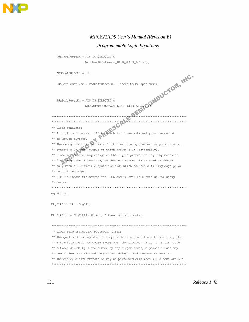
MPC821ADS User’s Manual (Revision B)
121
Release 1.4b
Programmable Logic Equations
PdaHardResetEn = ADS_IS_SELECTED &
(AdsHardReset==ADS_HARD_RESET_ACTIVE);
!PdaSoftReset~ = H;
PdaSoftReset~.oe = PdaSoftResetEn; "needs to be open-drain
PdaSoftResetEn = ADS_IS_SELECTED &
(AdsSoftReset==ADS_SOFT_RESET_ACTIVE );
"******************************************************************************
"******************************************************************************
"* Clock generator.
"* All i/f logic works on IClk, which is driven externally by the output
"* of DbgClk divider.
"* The debug clock divider is a 3 bit free-running counter, outputs of which
"* control a 4:1 mux, output of which drives IClk (externally).
"* Since mux control may change on the fly, a protection logic by means of
"* 2 bit register is provided, so that mux control is allowed to change
"* only when all divider outputs are high which assures a falling edge prior
"* to a rising edge.
"* Clk2 is infact the source for DSCK and is available outside for debug
"* purpose.
"******************************************************************************
equations
DbgClkDiv.clk = DbgClk;
DbgClkDiv := DbgClkDiv.fb + 1; " free running counter.
"******************************************************************************
"* Clock Safe Transition Register. (CSTR)
"* The goal of this register is to provide safe clock transitions, i.e., that
"* a trasition will not cause races over the clockout. E.g., in a transition
"* between divide by 1 and divide by any bigger order, a possible race may
"* occur since the divided outputs are delayed with respect to DbgClk.
"* Therefore, a safe transition may be performed only when all clocks are LOW.
"******************************************************************************
ARCHIVED BY FREESCALE SEMICONDUCTOR, INC.
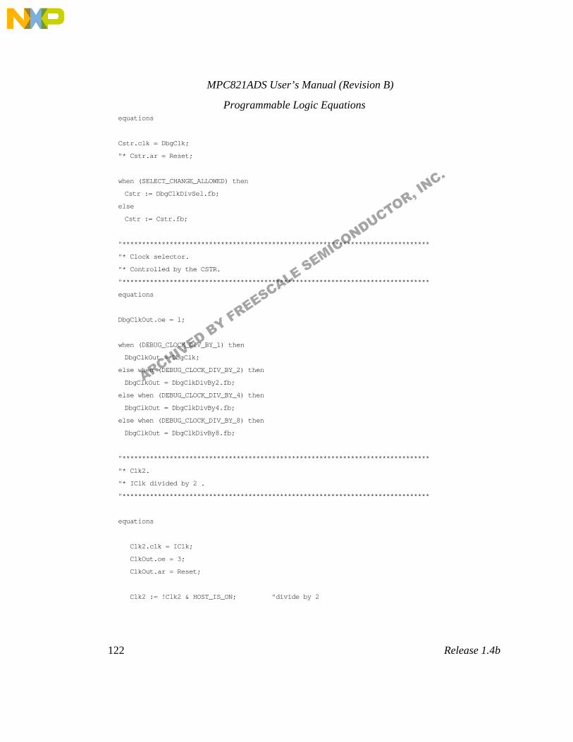
MPC821ADS User’s Manual (Revision B)
122
Release 1.4b
Programmable Logic Equations
equations
Cstr.clk = DbgClk;
"* Cstr.ar = Reset;
when (SELECT_CHANGE_ALLOWED) then
Cstr := DbgClkDivSel.fb;
else
Cstr := Cstr.fb;
"******************************************************************************
"* Clock selector.
"* Controlled by the CSTR.
"******************************************************************************
equations
DbgClkOut.oe = 1;
when (DEBUG_CLOCK_DIV_BY_1) then
DbgClkOut = DbgClk;
else when (DEBUG_CLOCK_DIV_BY_2) then
DbgClkOut = DbgClkDivBy2.fb;
else when (DEBUG_CLOCK_DIV_BY_4) then
DbgClkOut = DbgClkDivBy4.fb;
else when (DEBUG_CLOCK_DIV_BY_8) then
DbgClkOut = DbgClkDivBy8.fb;
"******************************************************************************
"* Clk2.
"* IClk divided by 2 .
"******************************************************************************
equations
Clk2.clk = IClk;
ClkOut.oe = 3;
ClkOut.ar = Reset;
Clk2 := !Clk2 & HOST_IS_ON; "divide by 2
ARCHIVED BY FREESCALE SEMICONDUCTOR, INC.
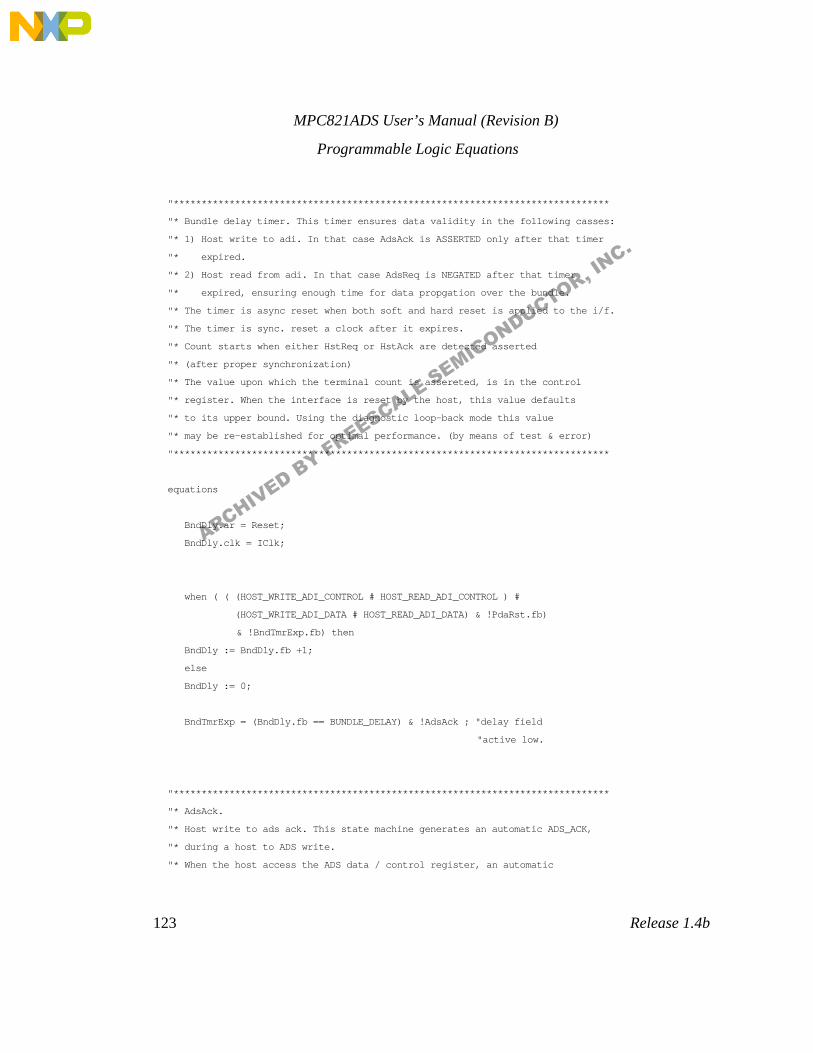
MPC821ADS User’s Manual (Revision B)
123
Release 1.4b
Programmable Logic Equations
"******************************************************************************
"* Bundle delay timer. This timer ensures data validity in the following casses:
"* 1) Host write to adi. In that case AdsAck is ASSERTED only after that timer
"* expired.
"* 2) Host read from adi. In that case AdsReq is NEGATED after that timer
"* expired, ensuring enough time for data propgation over the bundle.
"* The timer is async reset when both soft and hard reset is applied to the i/f.
"* The timer is sync. reset a clock after it expires.
"* Count starts when either HstReq or HstAck are detected asserted
"* (after proper synchronization)
"* The value upon which the terminal count is assereted, is in the control
"* register. When the interface is reset by the host, this value defaults
"* to its upper bound. Using the diagnostic loop-back mode this value
"* may be re-established for optimal performance. (by means of test & error)
"******************************************************************************
equations
BndDly.ar = Reset;
BndDly.clk = IClk;
when ( ( (HOST_WRITE_ADI_CONTROL # HOST_READ_ADI_CONTROL ) #
(HOST_WRITE_ADI_DATA # HOST_READ_ADI_DATA) & !PdaRst.fb)
& !BndTmrExp.fb) then
BndDly := BndDly.fb +1;
else
BndDly := 0;
BndTmrExp = (BndDly.fb == BUNDLE_DELAY) & !AdsAck ; "delay field
"active low.
"******************************************************************************
"* AdsAck.
"* Host write to ads ack. This state machine generates an automatic ADS_ACK,
"* during a host to ADS write.
"* When the host access the ADS data / control register, an automatic
ARCHIVED BY FREESCALE SEMICONDUCTOR, INC.
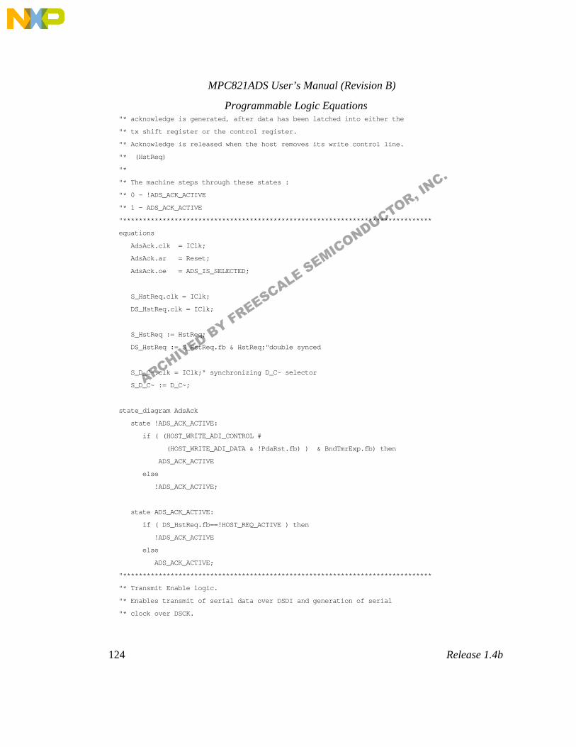
MPC821ADS User’s Manual (Revision B)
124
Release 1.4b
Programmable Logic Equations
"* acknowledge is generated, after data has been latched into either the
"* tx shift register or the control register.
"* Acknowledge is released when the host removes its write control line.
"* (HstReq)
"*
"* The machine steps through these states :
"* 0 - !ADS_ACK_ACTIVE
"* 1 - ADS_ACK_ACTIVE
"******************************************************************************
equations
AdsAck.clk = IClk;
AdsAck.ar = Reset;
AdsAck.oe = ADS_IS_SELECTED;
S_HstReq.clk = IClk;
DS_HstReq.clk = IClk;
S_HstReq := HstReq;
DS_HstReq := S_HstReq.fb & HstReq;"double synced
S_D_C~.clk = IClk;" synchronizing D_C~ selector
S_D_C~ := D_C~;
state_diagram AdsAck
state !ADS_ACK_ACTIVE:
if ( (HOST_WRITE_ADI_CONTROL #
(HOST_WRITE_ADI_DATA & !PdaRst.fb) ) & BndTmrExp.fb) then
ADS_ACK_ACTIVE
else
!ADS_ACK_ACTIVE;
state ADS_ACK_ACTIVE:
if ( DS_HstReq.fb==!HOST_REQ_ACTIVE ) then
!ADS_ACK_ACTIVE
else
ADS_ACK_ACTIVE;
"******************************************************************************
"* Transmit Enable logic.
"* Enables transmit of serial data over DSDI and generation of serial
"* clock over DSCK.
ARCHIVED BY FREESCALE SEMICONDUCTOR, INC.
MPC821ADS User’s Manual (Revision B)
125
Release 1.4b
Programmable Logic Equations
"* Transmission begins immediately after data written by the host is latched
"* into the transmit shift register and ends after 7 shifts were made to the
"* tx shift register.
"* Termination is done using a 4 bit counter TxWordLength which has a terminal
"* count (and reset) TxWordEnd.
"******************************************************************************
equations
TxEn.ar = Reset;
TxEn.clk = IClk;" to provide 1/2 clock resolution
state_diagram TxEn
state TX_DISABLED:
if(HOST_WRITE_ADI_DATA & BndTmrExp.fb & !PdaRst.fb) then
TX_ENABLED
else
TX_DISABLED;
state TX_ENABLED:
if(TxWordEnd # PdaRst.fb) then
TX_DISABLED
else
TX_ENABLED;
"******************************************************************************
"* Transmit Length Counter. This counter determines the length of transmission
"* towards the MPC821. The fast clock is used here to allow 1/2 clock resolution
"* with the negation of TxEn, which enables DSCK outside.
"******************************************************************************
equations
TxWordLen.ar = Reset;
TxWordLen.clk = IClk;
TxWordEnd = (TxWordLen.fb == TX_WORD_LENGTH);
when ( STATE_TX_ENABLED & !TxWordEnd & !PdaRst.fb) then
TxWordLen.d = TxWordLen.fb + 1;
else
TxWordLen.d = 0;
"******************************************************************************
ARCHIVED BY FREESCALE SEMICONDUCTOR, INC.

MPC821ADS User’s Manual (Revision B)
126
Release 1.4b
Programmable Logic Equations
"* TxClkSns - Transmit Clock Sense.
"* Since Host req is synced acc to IClk and may be detected active when Clk2 is
"* either '1' or '0', DSCK and the clock according to which DSDI is sent and
"* DSDO is sampled should be changed.
"* When TxClkSns is '0' - DSCK will be !Clk2 while transmit will be done
"* according to Clk2 and recieve by !Clk2.
"* When TxClkSns is '1' - DSCK will be Clk2 while transmit will be done
"* according to !Clk2~ and recieve by Clk2.
"******************************************************************************
equations
TxClkSns.clk = IClk;
TxClkSns.ar = Reset;
state_diagram TxClkSns
state TX_ON_RISING:
if (HOST_WRITE_ADI_DATA & BndTmrExp.fb & Clk2) then
TX_ON_FALLING
else
TX_ON_RISING;
state TX_ON_FALLING:
if (HOST_WRITE_ADI_DATA & BndTmrExp.fb & !Clk2) then
TX_ON_RISING
else
TX_ON_FALLING;
"******************************************************************************
"* Tx shift Register.
"* 8 bits shift register which either shifts data out (MSB first) or holds
"* its data. The edge (in Clk2 terms) upon which the above actions are taken,
"* is determined by TxClkSns. The Tx shift register operates according to IClk.
"* The Tx shift register is 1'st written by the host (data cycle) and along
"* with write being acknowledged to the host data is shifted out via DSDI.
"*
"* In order of saving logic, the Tx shift register is shared with the Receive
"* shift register, this, due to the fact that when a bit is shifted out a FF
"* becomes available. Since the Tx shift register is shifted MSB first, its
ARCHIVED BY FREESCALE SEMICONDUCTOR, INC.
MPC821ADS User’s Manual (Revision B)
127
Release 1.4b
Programmable Logic Equations
"* LSB FFs are grdualy becoming available for received data.
"* To provide a 1/2 DSCK hold time for DSDI, a single FF receive SR is used
"* which is the source for the Tx shift register. (if 0 hold is required
"* for DSDI this FF may be ommited)
"******************************************************************************
equations
TxReg.clk = IClk;
TxReg.ar = Reset;
when ( HOST_WRITE_ADI_DATA & BndTmrExp.fb & !STATE_TX_ENABLED) then
[TxReg7..TxReg1] := [PD7..PD1].pin; " latching ADI data
else when (STATE_TX_ENABLED & STATE_TX_ON_RISING & !Clk2 #
STATE_TX_ENABLED & STATE_TX_ON_FALLING & Clk2) then
[TxReg7..TxReg1] := [TxReg6..TxReg0].fb; " shifting out MSB 1'st.
else
[TxReg7..TxReg1] := [TxReg7..TxReg1].fb; " Holding value.
when ( HOST_WRITE_ADI_DATA & BndTmrExp.fb & !STATE_TX_ENABLED) then
TxReg0 := PD0.pin;
else when (STATE_TX_ENABLED & STATE_TX_ON_RISING & !Clk2 #
STATE_TX_ENABLED & STATE_TX_ON_FALLING & Clk2) then
TxReg0 := RxReg0.fb;
else
TxReg0 := TxReg0.fb;
"******************************************************************************
"* Receive Shift Register.
"* A single stage shift register used as a source for the Tx shift register.
"* In normal mode the input for the Rx shift register is the pda's DSDO, while
"* in diagnostic loopback mode, data is taken directly from the Tx shift
"* serial output.
"*
"* The output of the Rx shift register is fed to the input of the Tx shift
"* register. When transmission (and reception) is done the received data
"* word is compossed of the Rx shift register (LSB) concatenated with the
"* 7 LSBs of the Tx shift register.
"*
ARCHIVED BY FREESCALE SEMICONDUCTOR, INC.
MPC821ADS User’s Manual (Revision B)
128
Release 1.4b
Programmable Logic Equations
"* The edge (in Clk2 terms) upon which data is shifted in is determined by
"* TxClkSns as with the Tx shift register but on opposite edges, i.e.,
"* data is shifted Out from the Tx shift register on the Falling edge of
"* DSCK while is shifted In to the Rx shift register on the Rising edge
"* DSCK. (DSCK terms are constant in that regard).
"******************************************************************************
equations
RxReg0.clk = IClk;
RxReg0.ar = Reset;
when ( STATE_TX_ENABLED & STATE_TX_ON_RISING & Clk2 #
STATE_TX_ENABLED & STATE_TX_ON_FALLING & !Clk2) & (!IN_DIAG_LOOP_BACK) then
RxReg0.d = DSDO; "shift in ext data
else when ( STATE_TX_ENABLED & STATE_TX_ON_RISING & Clk2 #
STATE_TX_ENABLED & STATE_TX_ON_FALLING & !Clk2) & IN_DIAG_LOOP_BACK then
RxReg0.d = TxReg7.fb;" shift in from transmit reg
else
RxReg0.d = RxReg0.fb;" hold value
"******************************************************************************
"* AdsReq.
"* Host from ads, read acknowledge. This state machine generates an automatic
"* ADS read request from the host when either a byte of data is received in the
"* Rx shift register or the status request bit in the control register is
"* active during a previous host write to the control register.
"* When the host detectes AdsReq asserted, it assertes HstAck in return. HstAck
"* double synchronized from the ADI port and delayed using the bundle delay
"* compensation timer to negate AdsReq. When the host detects AdsReq negated
"* it knows that data is valid to be read. After the host reads the data it
"* negates HstAck.
"* The machine steps through these states :
"* 0 - !ADS_REQ_ACTIVE
"* 1 - ADS_REQ_ACTIVE
"******************************************************************************
equations
AdsReq.clk = IClk;
AdsReq.ar = Reset;
AdsReq.oe = ADS_IS_SELECTED;
ARCHIVED BY FREESCALE SEMICONDUCTOR, INC.
MPC821ADS User’s Manual (Revision B)
129
Release 1.4b
Programmable Logic Equations
S_HstAck.clk = IClk;
DS_HstAck.clk = IClk;
S_HstAck := HstAck;
DS_HstAck := HstAck & S_HstAck;"double synced
state_diagram AdsReq
state !ADS_REQ_ACTIVE:
if ( TxEn.fb & TxWordEnd #" end of data shift to PDA
ADS_SEND_STATUS) then" end of control write and status required
ADS_REQ_ACTIVE
else
!ADS_REQ_ACTIVE;
state ADS_REQ_ACTIVE:
if ( HOST_READ_ADI & BndTmrExp.fb ) then
!ADS_REQ_ACTIVE
else
ADS_REQ_ACTIVE;
"******************************************************************************
"* ADI control register.
"* The ADI control register is written upon host to ADI write with a
"* D_C~ line is in control mode. It also may be read when StatusRequest~ bit
"* is active.
"*
"* Control register bits description:
"*
"* DebugEntry~: (Bit 0). When this bit is active (L), the pda will enter debug
"* mode immediately after reset, i.e., DSCK will be held high
"* after the rising edge of SRESET*. When negated, DSCK will be
"* held low after the rising edge of SRESET so the pda will start
"* running instantly.
"* DiagLoopBack~: (Bit 1). When active (L), the interface is in Diagnostic
"* Loopback mode. I.e., the source for the Rx shift register is
"* the output of the Tx shift register. During that mode, DSCK
"* and DSDI are tri-stated, so no arbitrary data is sent to the
"* debug port. When inactive, the interface is in normal mode,
"* i.e., DSCK and DSDI are driven and the source of the Rx shift
ARCHIVED BY FREESCALE SEMICONDUCTOR, INC.
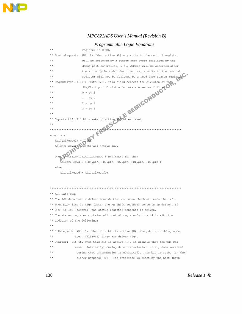
MPC821ADS User’s Manual (Revision B)
130
Release 1.4b
Programmable Logic Equations
"* register is DSDO.
"* StatusRequest~: (Bit 2). When active (L) any write to the control register
"* will be followed by a status read cycle initiated by the
"* debug port controller, i.e., AdsReq will be asserted after
"* the write cycle ends. When inactive, a write to the control
"* register will not be followed by a read from status register.
"* DbgClkDivSel(1:0) : (Bits 4,3). This field selects the division of the
"* DbgClk input. Division factors are set as follows:
"* 0 - by 1
"* 1 - by 2
"* 2 - by 4
"* 3 - by 8
"*
"* Important!!! All bits wake up active (L) after reset.
"*
"******************************************************************************
equations
AdiCtrlReg.clk = IClk;
AdiCtrlReg.ar = Reset;"All active low.
when ( HOST_WRITE_ADI_CONTROL & BndTmrExp.fb) then
AdiCtrlReg.d = [PD4.pin, PD3.pin, PD2.pin, PD1.pin, PD0.pin];
else
AdiCtrlReg.d = AdiCtrlReg.fb;
"******************************************************************************
"* ADI Data Bus.
"* The Adi data bus is driven towards the host when the host reads the i/f.
"* When D_C~ line is high (data) the Rx shift register contents is driven. If
"* D_C~ is low (control) the status register contents is driven.
"* The status register contains all control register's bits (4:0) with the
"* addition of the following:
"*
"* InDebugMode: (Bit 5). When this bit is active (H), the pda is in debug mode,
"* i.e., VFLS(0:1) lines are driven high.
"* TxError: (Bit 6). When this bit is active (H), it signals that the pda was
"* reset (internally) during data transmission. (i.e., data received
"* during that trnasmission is corrupted). This bit is reset (L) when
"* either happens: (1) - The interface is reset by the host (both
ARCHIVED BY FREESCALE SEMICONDUCTOR, INC.
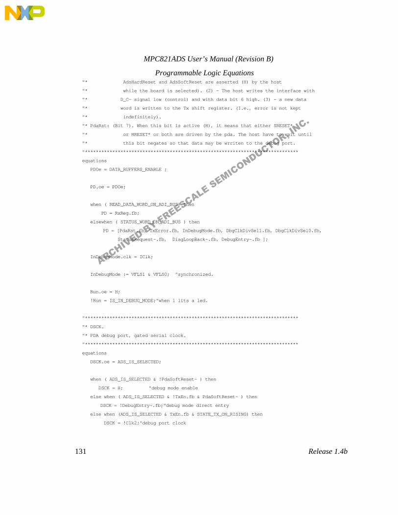
MPC821ADS User’s Manual (Revision B)
131
Release 1.4b
Programmable Logic Equations
"* AdsHardReset and AdsSoftReset are asserted (H) by the host
"* while the board is selected). (2) - The host writes the interface with
"* D_C~ signal low (control) and with data bit 6 high. (3) - a new data
"* word is written to the Tx shift register. (I.e., error is not kept
"* indefinitely).
"* PdaRst: (Bit 7). When this bit is active (H), it means that either SRESET*
"* or HRESET* or both are driven by the pda. The host have to wait until
"* this bit negates so that data may be wrriten to the debug port.
"******************************************************************************
equations
PDOe = DATA_BUFFERS_ENABLE ;
PD.oe = PDOe;
when ( READ_DATA_WORD_ON_ADI_BUS) then
PD = RxReg.fb;
elsewhen ( STATUS_WORD_ON_ADI_BUS ) then
PD = [PdaRst.fb, TxError.fb, InDebugMode.fb, DbgClkDivSel1.fb, DbgClkDivSel0.fb,
StatusRequest~.fb, DiagLoopBack~.fb, DebugEntry~.fb ];
InDebugMode.clk = IClk;
InDebugMode := VFLS1 & VFLS0; "synchronized.
Run.oe = H;
!Run = IS_IN_DEBUG_MODE;"when 1 lits a led.
"******************************************************************************
"* DSCK.
"* PDA debug port, gated serial clock.
"******************************************************************************
equations
DSCK.oe = ADS_IS_SELECTED;
when ( ADS_IS_SELECTED & !PdaSoftReset~ ) then
DSCK = H; "debug mode enable
else when ( ADS_IS_SELECTED & !TxEn.fb & PdaSoftReset~ ) then
DSCK = !DebugEntry~.fb;"debug mode direct entry
else when (ADS_IS_SELECTED & TxEn.fb & STATE_TX_ON_RISING) then
DSCK = !Clk2;"debug port clock
ARCHIVED BY FREESCALE SEMICONDUCTOR, INC.
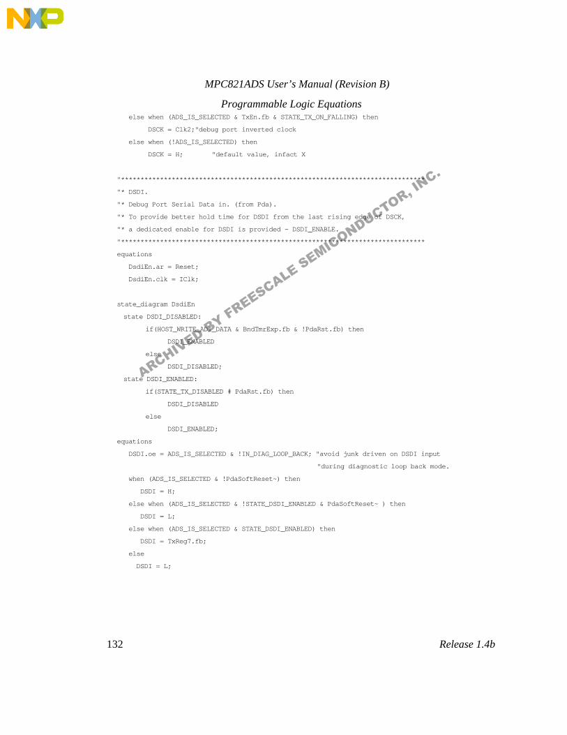
MPC821ADS User’s Manual (Revision B)
132
Release 1.4b
Programmable Logic Equations
else when (ADS_IS_SELECTED & TxEn.fb & STATE_TX_ON_FALLING) then
DSCK = Clk2;"debug port inverted clock
else when (!ADS_IS_SELECTED) then
DSCK = H; "default value, infact X
"******************************************************************************
"* DSDI.
"* Debug Port Serial Data in. (from Pda).
"* To provide better hold time for DSDI from the last rising edge of DSCK,
"* a dedicated enable for DSDI is provided - DSDI_ENABLE.
"******************************************************************************
equations
DsdiEn.ar = Reset;
DsdiEn.clk = IClk;
state_diagram DsdiEn
state DSDI_DISABLED:
if(HOST_WRITE_ADI_DATA & BndTmrExp.fb & !PdaRst.fb) then
DSDI_ENABLED
else
DSDI_DISABLED;
state DSDI_ENABLED:
if(STATE_TX_DISABLED # PdaRst.fb) then
DSDI_DISABLED
else
DSDI_ENABLED;
equations
DSDI.oe = ADS_IS_SELECTED & !IN_DIAG_LOOP_BACK; "avoid junk driven on DSDI input
"during diagnostic loop back mode.
when (ADS_IS_SELECTED & !PdaSoftReset~) then
DSDI = H;
else when (ADS_IS_SELECTED & !STATE_DSDI_ENABLED & PdaSoftReset~ ) then
DSDI = L;
else when (ADS_IS_SELECTED & STATE_DSDI_ENABLED) then
DSDI = TxReg7.fb;
else
DSDI = L;
ARCHIVED BY FREESCALE SEMICONDUCTOR, INC.

MPC821ADS User’s Manual (Revision B)
133
Release 1.4b
Programmable Logic Equations
"******************************************************************************
"* TxError.
"* This bit of the status register is set ('1') when the pda internally resets
"* during data transmission over the debug port.
"* When this bit is writen '1' by the adi port (control) the status bit is
"* cleared. Writing '0' has no influence on that bit.
"******************************************************************************
equations
TxError.clk = IClk;
TxError.ar = Reset;
state_diagram TxError
state TX_DONE_OK:
if(STATE_TX_ENABLED & PdaRst.fb) then
TX_INTERRUPTED
else
TX_DONE_OK;
state TX_INTERRUPTED:
if (HOST_WRITE_ADI_CONTROL & BndTmrExp.fb & PD6.pin
# HOST_WRITE_ADI_DATA & BndTmrExp.fb & !PdaRst.fb) then
TX_DONE_OK
else
TX_INTERRUPTED;
end dbg_prt7
ARCHIVED BY FREESCALE SEMICONDUCTOR, INC.
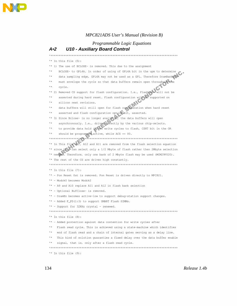
MPC821ADS User’s Manual (Revision B)
134
Release 1.4b
Programmable Logic Equations
A•2 U10 - Auxiliary Board Control
"******************************************************************************
"* In this file (5):
"* 1) The use of BCLOSE~ is removed. This due to the assignment
"* BCLOSE~ to GPL4A. In order of using of GPL4A bit in the upm to determine
"* data sampling edge, GPL4A may not be used as a GPL. Therefore DramBankXCs~
"* must envelope the cycle so that data buffers remain open throughout the
"* cycle.
"* 2) Removed CS support for flash configuration. I.e., FlashCs1~ will not be
"* asserted during hard reset. Flash configuration will be supported on
"* silicon next revisions.
"* data buffers will still open for flash configuration when hard reset
"* asserted and flash configuration option bit, asserted.
"* 3) Since Bclose~ is no longer available, the data buffers will open
"* asynchronously. I.e., driven directly by the various chip-selects.
"* to provide data hold (0) on write cycles to flash, CSNT bit in the OR
"* should be programmed active, while ACS == 00.
"******************************************************************************
"* In This file (6), A12 and A11 are removed from the flash selection equation
"* since they can select only a 1/2 Mbyte of flash rather then 2Mbyte selection
"* needed. Therefore, only one bank of 2 Mbyte flash may be used (MCM29F020).
"* The rest of the CS are driven high constantly.
"******************************************************************************
"* In this file (7):
"* - Pon Reset Out is removed. Pon Reset is driven directly to MPC821.
"* - Modck0 becomes Modck2
"* - A9 and A10 replace A11 and A12 in flash bank selection
"* - Optional BufClose~ is removed.
"* - DramEn becomes active-low to support debug-station support changes.
"* - Added F_PD(1:3) to support SMART Flash SIMMs.
"* - Support for 32KHz crystal - renewed.
"******************************************************************************
"* In this file (8):
"* - Added protection against data contention for write cycles after
"* Flash read cycle. This is achieved using a state-machine which identifies
"* end of flash read and a chain of internal gates serving as a delay line.
"* This kind of solution guaranties a fixed delay over the data buffer enable
"* signal, that is, only after a flash read cycle.
"******************************************************************************
"* In this file (9):
ARCHIVED BY FREESCALE SEMICONDUCTOR, INC.
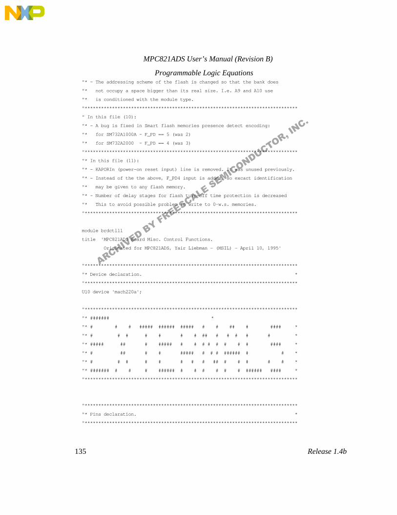
MPC821ADS User’s Manual (Revision B)
135
Release 1.4b
Programmable Logic Equations
"* - The addressing scheme of the flash is changed so that the bank does
"* not occupy a space bigger than its real size. I.e. A9 and A10 use
"* is conditioned with the module type.
"******************************************************************************
" In this file (10):
"* - A bug is fixed in Smart flash memories presence detect encoding:
"* for SM732A1000A - F_PD == 5 (was 2)
"* for SM732A2000 - F_PD == 4 (was 3)
"******************************************************************************
"* In this file (11):
"* - KAPORIn (power-on reset input) line is removed. It was unused previously.
"* - Instead of the the above, F_PD4 input is added, so excact identification
"* may be given to any flash memory.
"* - Number of delay stages for flash turn-off time protection is decreased
"* This to avoid possible problem in write to 0-w.s. memories.
"******************************************************************************
module brdctl11
title 'MPC821ADS Board Misc. Control Functions.
Originated for MPC821ADS, Yair Liebman - (MSIL) - April 10, 1995'
"******************************************************************************
"* Device declaration. *
"******************************************************************************
U10 device 'mach220a';
"******************************************************************************
"* ####### *
"* # # # ##### ###### ##### # # ## # #### *
"* # # # # # # # ## # # # # # *
"* ##### ## # ##### # # # # # # # # #### *
"* # ## # # ##### # # # ###### # # *
"* # # # # # # # # ## # # # # # *
"* ####### # # # ###### # # # # # # ###### #### *
"******************************************************************************
"******************************************************************************
"* Pins declaration. *
"******************************************************************************
ARCHIVED BY FREESCALE SEMICONDUCTOR, INC.
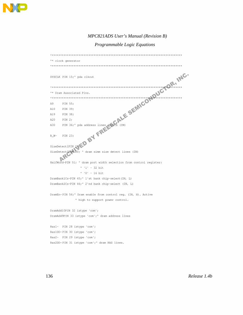
MPC821ADS User’s Manual (Revision B)
136
Release 1.4b
Programmable Logic Equations
"******************************************************************************
"* clock generator
"******************************************************************************
SYSCLK PIN 15;" pda clkout
"******************************************************************************
"* Dram Associated Pins.
"******************************************************************************
A9 PIN 55;
A10 PIN 39;
A19 PIN 38;
A20 PIN 2;
A30 PIN 36;" pda address lines inputs (IN)
R_W~ PIN 23;
SizeDetect1PIN 26;
SizeDetect0PIN 20; " dram simm size detect lines (IN)
HalfWord~PIN 51; " dram port width selection from control register:
" '1' - 32 bit
" '0' - 16 bit
DramBank1Cs~PIN 45;" 1'st bank chip-select(IN, L)
DramBank2Cs~PIN 46;" 2'nd bank chip-select (IN, L)
DramEn~ PIN 54;" Dram enable from control reg. (IN, H). Active
" high to support power control.
DramAdd10PIN 32 istype 'com';
DramAdd9PIN 33 istype 'com';" dram address lines
Ras1~ PIN 28 istype 'com';
Ras1DD~ PIN 30 istype 'com';
Ras2~ PIN 29 istype 'com';
Ras2DD~ PIN 31 istype 'com';" dram RAS lines.
ARCHIVED BY FREESCALE SEMICONDUCTOR, INC.
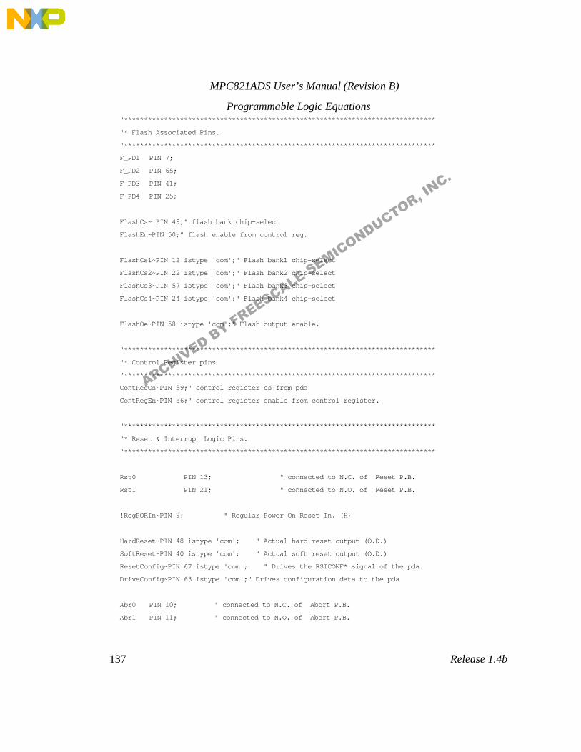
MPC821ADS User’s Manual (Revision B)
137
Release 1.4b
Programmable Logic Equations
"******************************************************************************
"* Flash Associated Pins.
"******************************************************************************
F_PD1 PIN 7;
F_PD2 PIN 65;
F_PD3 PIN 41;
F_PD4 PIN 25;
FlashCs~ PIN 49;" flash bank chip-select
FlashEn~PIN 50;" flash enable from control reg.
FlashCs1~PIN 12 istype 'com';" Flash bank1 chip-select
FlashCs2~PIN 22 istype 'com';" Flash bank2 chip-select
FlashCs3~PIN 57 istype 'com';" Flash bank3 chip-select
FlashCs4~PIN 24 istype 'com';" Flash bank4 chip-select
FlashOe~PIN 58 istype 'com';" Flash output enable.
"******************************************************************************
"* Control Register pins
"******************************************************************************
ContRegCs~PIN 59;" control register cs from pda
ContRegEn~PIN 56;" control register enable from control register.
"******************************************************************************
"* Reset & Interrupt Logic Pins.
"******************************************************************************
Rst0 PIN 13; " connected to N.C. of Reset P.B.
Rst1 PIN 21; " connected to N.O. of Reset P.B.
!RegPORIn~PIN 9; " Regular Power On Reset In. (H)
HardReset~PIN 48 istype 'com'; " Actual hard reset output (O.D.)
SoftReset~PIN 40 istype 'com'; " Actual soft reset output (O.D.)
ResetConfig~PIN 67 istype 'com'; " Drives the RSTCONF* signal of the pda.
DriveConfig~PIN 63 istype 'com';" Drives configuration data to the pda
Abr0 PIN 10; " connected to N.C. of Abort P.B.
Abr1 PIN 11; " connected to N.O. of Abort P.B.
ARCHIVED BY FREESCALE SEMICONDUCTOR, INC.
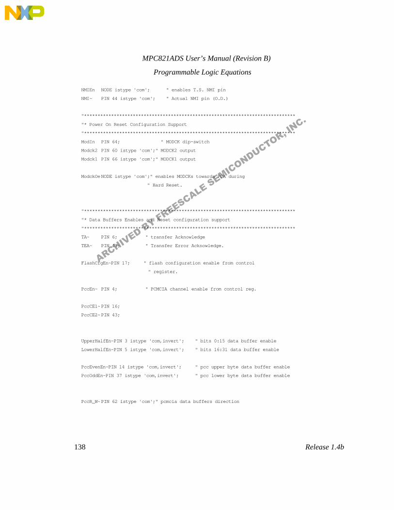
MPC821ADS User’s Manual (Revision B)
138
Release 1.4b
Programmable Logic Equations
NMIEn NODE istype 'com'; " enables T.S. NMI pin
NMI~ PIN 44 istype 'com'; " Actual NMI pin (O.D.)
"******************************************************************************
"* Power On Reset Configuration Support
"******************************************************************************
ModIn PIN 64; " MODCK dip-switch
Modck2 PIN 60 istype 'com';" MODCK2 output
Modck1 PIN 66 istype 'com';" MODCK1 output
ModckOe NODE istype 'com';" enables MODCKs towards PDA during
" Hard Reset.
"******************************************************************************
"* Data Buffers Enables and Reset configuration support
"******************************************************************************
TA~ PIN 6; " transfer Acknowledge
TEA~ PIN 47; " Transfer Error Acknowledge.
FlashCfgEn~PIN 17; " flash configuration enable from control
" register.
PccEn~ PIN 4; " PCMCIA channel enable from control reg.
PccCE1~ PIN 16;
PccCE2~ PIN 43;
UpperHalfEn~PIN 3 istype 'com,invert'; " bits 0:15 data buffer enable
LowerHalfEn~PIN 5 istype 'com,invert'; " bits 16:31 data buffer enable
PccEvenEn~PIN 14 istype 'com,invert'; " pcc upper byte data buffer enable
PccOddEn~PIN 37 istype 'com,invert'; " pcc lower byte data buffer enable
PccR_W~ PIN 62 istype 'com';" pcmcia data buffers direction
ARCHIVED BY FREESCALE SEMICONDUCTOR, INC.
MPC821ADS User’s Manual (Revision B)
139
Release 1.4b
Programmable Logic Equations
"******************************************************************************
"* ### *
"* # # # ##### ###### ##### # # ## # #### *
"* # ## # # # # # ## # # # # # *
"* # # # # # ##### # # # # # # # # #### *
"* # # # # # # ##### # # # ###### # # *
"* # # ## # # # # # ## # # # # # *
"* ### # # # ###### # # # # # # ###### #### *
"******************************************************************************
"******************************************************************************
"* Reset & Interrupt Logic Pins.
"******************************************************************************
RstDeb1 NODE istype 'com'; " reset push button debouncer
AbrDeb1 NODE istype 'com'; " abort push button debouncer
HardResetEnNODE istype 'com'; " enables T.S. hard reset pin
SoftResetEnNODE istype 'com'; " enables T.S. soft reset pin
ConfigHold2,
ConfigHold1,
ConfigHold0node istype 'reg,buffer';" supplies data hold time for
" hard reset configuration
ConfigHoldEndnode istype 'com';
"******************************************************************************
"* data buffers enable.
"******************************************************************************
SyncHardReset~NODE istype 'reg,buffer'; " synchronized hard reset
DSyncHardReset~ NODE istype 'reg,buffer';" double synchronized hard reset
SyncTEA~NODE istype 'reg,buffer';" needed since TEA~ is O.D.
HoldOffConsidered NODE istype 'reg,buffer';" data drive hold-off state
" machine.
ARCHIVED BY FREESCALE SEMICONDUCTOR, INC.
MPC821ADS User’s Manual (Revision B)
140
Release 1.4b
Programmable Logic Equations
D_FlashOe~NODE istype 'com'; " delayed flash output enable
DD_FlashOe~NODE istype 'com';" double delayed flash output
" enable
TD_FlashOe~NODE istype 'com';" triple delayed flash output
" enable
" QD_FlashOe~NODE istype 'com'; quad delayed
" PD_FlashOe~NODE istype 'com'; penta delayed
KeepPinsConnected node istype 'com';
"******************************************************************************
"* ##### *
"* # # #### # # #### ##### ## # # ##### *
"* # # # ## # # # # # ## # # *
"* # # # # # # #### # # # # # # # *
"* # # # # # # # # ###### # # # # *
"* # # # # # ## # # # # # # ## # *
"* ##### #### # # #### # # # # # # *
"* *
"* ###### *
"* # # ###### #### # ## ##### *
"* # # # # # # # # # # *
"* # # ##### # # # # # # ##### *
"* # # # # # ###### ##### *
"* # # # # # # # # # # *
"* ###### ###### #### ###### # # # # *
"* *
"* ## ##### # #### # # *
"* # # # # # # ## # *
"* # # # # # # # # # *
"* ###### # # # # # # # *
"* # # # # # # # ## *
"* # # # # #### # # *
"******************************************************************************
H, L, X, Z = 1, 0, .X., .Z.;
C, D, U = .C., .D., .U.;
"******************************************************************************
"* SLOW_32K_LOCK = 1;
"******************************************************************************
ARCHIVED BY FREESCALE SEMICONDUCTOR, INC.
MPC821ADS User’s Manual (Revision B)
141
Release 1.4b
Programmable Logic Equations
"* Signal groups
"******************************************************************************
PdaAdd = [A9,A10,A19,A20,A30];
DramAdd = [DramAdd10,DramAdd9];
DramCS~ =[DramBank2Cs~,DramBank1Cs~];
RAS = [Ras1~,Ras1DD~,Ras2~,Ras2DD~];
SD = [SizeDetect1,SizeDetect0];
FlashCsOut = [FlashCs4~,FlashCs3~,FlashCs2~,FlashCs1~];
Reset = [HardReset~,SoftReset~];
ResetEn = [HardResetEn,SoftResetEn];
Rst = [Rst1,Rst0];
Abr = [Abr1,Abr0];
Debounce = [RstDeb1,AbrDeb1];
DramCs = [DramBank2Cs~,DramBank1Cs~];
Cs = [ContRegCs~,FlashCs~ ,DramBank1Cs~,DramBank2Cs~];
PccCs = [PccCE1~,PccCE2~];
LocDataBufEn = [UpperHalfEn~,LowerHalfEn~];
PccDataBufEn = [PccEvenEn~,PccOddEn~];
ModuleEn = [DramEn~,FlashEn~,PccEn~,ContRegEn~];
SyncReset = [SyncHardReset~,DSyncHardReset~];
RstCause = [Rst1,Rst0,Abr1,Abr0,RegPORIn~];
Stp = [TA~];
Modck = [Modck2, Modck1];
ConfigHold =[ConfigHold2, ConfigHold1, ConfigHold0];
F_PD = [F_PD4, F_PD3, F_PD2, F_PD1];
"******************************************************************************
"* Dram Declarations.
"******************************************************************************
DRAM_ENABLE_ACTIVE = 0;
DRAM_ENABLED = (DramEn~ == DRAM_ENABLE_ACTIVE);
SIMM36100 = (SD == 0);
SIMM36200 = (SD == 3);
SIMM36400 = (SD == 2);
SIMM36800 = (SD == 1);
IS_HALF_WORD = (HalfWord~ == 0);
"******************************************************************************
ARCHIVED BY FREESCALE SEMICONDUCTOR, INC.
MPC821ADS User’s Manual (Revision B)
142
Release 1.4b
Programmable Logic Equations
"* Flash Declarations.
"******************************************************************************
FLASH_ENABLE_ACTIVE = 0;
FLASH_ENABLED = (FlashEn~ == FLASH_ENABLE_ACTIVE);
MCM29020 = (F_PD == 8);
MCM29040 = (F_PD == 7);
MCM29080 = (F_PD == 6);
SM732A1000A = (F_PD == 5);
SM732A2000 = (F_PD == 4);
FLASH_BANK1 = ( (MCM29020 # SM732A1000A) #
(MCM29040 & !A10) #
(MCM29080 & !A9 & !A10) #
(SM732A2000 & !A9) );
FLASH_BANK2 = ( (MCM29040 & A10) #
(MCM29080 & !A9 & A10) #
(SM732A2000 & A9) );
FLASH_BANK3 = (A9 & !A10 & MCM29080);
FLASH_BANK4 = (A9 & A10 & MCM29080);
"******************************************************************************
"* Reset Declarations.
"******************************************************************************
KEEP_ALIVE_PON_RESET_ACTIVE = 0;
REGULAR_PON_RESET_ACTIVE = 0;
HARD_RESET_ACTIVE = 0;
SOFT_RESET_ACTIVE = 0;
HARD_CONFIG_HOLD_VALUE = 4;
DRIVE_MODCK_TO_PDA = (HardReset~ == HARD_RESET_ACTIVE);" have modck stable
" during hard reset.
REGULAR_POWER_ON_RESET = (RegPORIn~ == REGULAR_PON_RESET_ACTIVE);
ARCHIVED BY FREESCALE SEMICONDUCTOR, INC.
MPC821ADS User’s Manual (Revision B)
143
Release 1.4b
Programmable Logic Equations
HARD_RESET_ASSERTED = (SyncHardReset~.fb == HARD_RESET_ACTIVE);
HARD_RESET_NEGATES = ( (SyncHardReset~.fb != HARD_RESET_ACTIVE )
& (DSyncHardReset~.fb == HARD_RESET_ACTIVE));
" detecting hard reset negation
"******************************************************************************
"* data buffers enable.
"******************************************************************************
BUFFER_DISABLED = 1;
BUFFER_ENABLED = !BUFFER_DISABLED;
CONTROL_REG_ENABLE_ACTIVE = 0;
FLASH_CONFIG_ENABLED_ACTIVE = 0;
PCMCIA_ENABLE_ACTIVE = 0;
GPL_ACTIVE = 0;
TEA_ASSERTS = (!TEA~ & SyncTEA~.fb);" first clock of TEA~ asserted
CONTROL_REG_ENABLED = (ContRegEn~ == CONTROL_REG_ENABLE_ACTIVE);
FLASH_CONFIGURATION_ENABLED = (FlashCfgEn~ == FLASH_CONFIG_ENABLED_ACTIVE);
PCC_ENABLED = (PccEn~ == PCMCIA_ENABLE_ACTIVE);
NO_HOLD_OFF = 0;
HOLD_OFF_CONSIDERED = 1;
STATE_HOLD_OFF_CONSIDERED = (HoldOffConsidered.fb == HOLD_OFF_CONSIDERED);
STATE_NO_HOLD_OFF = (HoldOffConsidered.fb == NO_HOLD_OFF);
END_OF_FLASH_READ = !TA~ & !FlashCs~ & R_W~;" end of flash read cycle.
END_OF_OTHER_CYCLE = (!TA~ & FlashCs~ # " another access or
!TA~ & !FlashCs~ & !R_W~); " flash write
"* HOLD_OFF_PERIOD = (!R_W~ & !PD_FlashOe~.fb);
ARCHIVED BY FREESCALE SEMICONDUCTOR, INC.
MPC821ADS User’s Manual (Revision B)
144
Release 1.4b
Programmable Logic Equations
HOLD_OFF_PERIOD = (!R_W~ & !TD_FlashOe~.fb);
"******************************************************************************
"* Equations, state diagrams. *
"******************************************************************************
"* *
"* ####### *
"* # #### # # ## ##### # #### # # #### *
"* # # # # # # # # # # # ## # # *
"* ##### # # # # # # # # # # # # # #### *
"* # # # # # # ###### # # # # # # # # *
"* # # # # # # # # # # # # ## # # *
"* ####### ### # #### # # # # #### # # #### *
"* *
"******************************************************************************
"* Reset Logic
"******************************************************************************
equations
Reset.oe = ResetEn;
Reset = 0;" open drain
RstDeb1 = !( Rst1 & (!( RstDeb1.fb & Rst0) ) ); " Reset push-button debouncer
AbrDeb1 = !( Abr1 & (!( AbrDeb1.fb & Abr0) ) ); " Abort push-button debouncer
HardResetEn = RstDeb1.fb & AbrDeb1.fb " both buttons are depressed;
# REGULAR_POWER_ON_RESET;
SoftResetEn = RstDeb1.fb & !AbrDeb1.fb;" only reset button depressed
"******************************************************************************
"* Power On reset configuration
"******************************************************************************
equations
ARCHIVED BY FREESCALE SEMICONDUCTOR, INC.
MPC821ADS User’s Manual (Revision B)
145
Release 1.4b
Programmable Logic Equations
Modck.oe = ModckOe;
ModckOe = DRIVE_MODCK_TO_PDA;
Modck2 = L;
@ifndef SLOW_32K_LOCK
Modck2 = ModIn;" support for 1:513 (32KHz crystal) or
Modck1 = ModIn;" 1:5 (5MHz clock gen.) via CLK4IN
@ifdef SLOW_32K_LOCK
Modck2 = !ModIn;" support for 1:1 or 1:5 from CLK4IN only
Modck1 = H; " no support for 32K oscillator.
"******************************************************************************
"* Hard reset configuration
"******************************************************************************
equations
ResetConfig~.oe = H;
DriveConfig~.oe = H;
"* Configuration hold counter. Since the rise time of the HARD RESET signal
"* is relatively slow, there is a need to provide a hold time for reset
"* configuration.
ConfigHold.clk = SYSCLK;
when (SyncHardReset~.fb & !ConfigHoldEnd.fb) then ConfigHold := ConfigHold.fb +1;
else when (SyncHardReset~.fb & ConfigHoldEnd.fb) then ConfigHold := ConfigHold.fb;
else when (!SyncHardReset~.fb) then ConfigHold := 0;
ConfigHoldEnd = (ConfigHold.fb == HARD_CONFIG_HOLD_VALUE); " terminal count
!ResetConfig~ = !HardReset~;" drives RSTCONF~ to pda
!DriveConfig~ = !ConfigHoldEnd.fb; " drives configuration data on the bus.
ARCHIVED BY FREESCALE SEMICONDUCTOR, INC.
MPC821ADS User’s Manual (Revision B)
146
Release 1.4b
Programmable Logic Equations
"******************************************************************************
"* NMI generation
"******************************************************************************
equations
NMI~.oe = NMIEn;
NMI~ = 0;" O.D.
NMIEn = !RstDeb1.fb & AbrDeb1.fb;" only abort button depressed
"******************************************************************************
"* local data buffers enable
"******************************************************************************
equations
SyncHardReset~.clk = SYSCLK;
DSyncHardReset~.clk = SYSCLK;
SyncHardReset~ := HardReset~;
DSyncHardReset~ := SyncHardReset~.fb;
SyncTEA~.clk = SYSCLK;
SyncTEA~ := TEA~;
LocDataBufEn.oe = 3;
!UpperHalfEn~ = (!DramBank1Cs~ & DRAM_ENABLED #
!DramBank2Cs~ & (SIMM36200 # SIMM36800) & DRAM_ENABLED #
!FlashCs~ & FLASH_ENABLED #
!ContRegCs~ & CONTROL_REG_ENABLED #
!PccCE1~ & PCC_ENABLED #
!PccCE2~ & PCC_ENABLED #
!ConfigHoldEnd.fb) &
(STATE_HOLD_OFF_CONSIDERED & (!HOLD_OFF_PERIOD) #
STATE_NO_HOLD_OFF);
ARCHIVED BY FREESCALE SEMICONDUCTOR, INC.
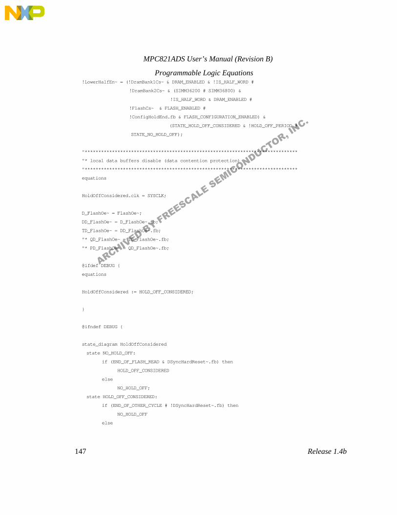
MPC821ADS User’s Manual (Revision B)
147
Release 1.4b
Programmable Logic Equations
!LowerHalfEn~ = (!DramBank1Cs~ & DRAM_ENABLED & !IS_HALF_WORD #
!DramBank2Cs~ & (SIMM36200 # SIMM36800) &
!IS_HALF_WORD & DRAM_ENABLED #
!FlashCs~ & FLASH_ENABLED #
!ConfigHoldEnd.fb & FLASH_CONFIGURATION_ENABLED) &
(STATE_HOLD_OFF_CONSIDERED & !HOLD_OFF_PERIOD #
STATE_NO_HOLD_OFF);
"******************************************************************************
"* local data buffers disable (data contention protection)
"******************************************************************************
equations
HoldOffConsidered.clk = SYSCLK;
D_FlashOe~ = FlashOe~;
DD_FlashOe~ = D_FlashOe~.fb;
TD_FlashOe~ = DD_FlashOe~.fb;
"* QD_FlashOe~ = TD_FlashOe~.fb;
"* PD_FlashOe~ = QD_FlashOe~.fb;
@ifdef DEBUG
equations
HoldOffConsidered := HOLD_OFF_CONSIDERED;
@ifndef DEBUG
state_diagram HoldOffConsidered
state NO_HOLD_OFF:
if (END_OF_FLASH_READ & DSyncHardReset~.fb) then
HOLD_OFF_CONSIDERED
else
NO_HOLD_OFF;
state HOLD_OFF_CONSIDERED:
if (END_OF_OTHER_CYCLE # !DSyncHardReset~.fb) then
NO_HOLD_OFF
else
ARCHIVED BY FREESCALE SEMICONDUCTOR, INC.
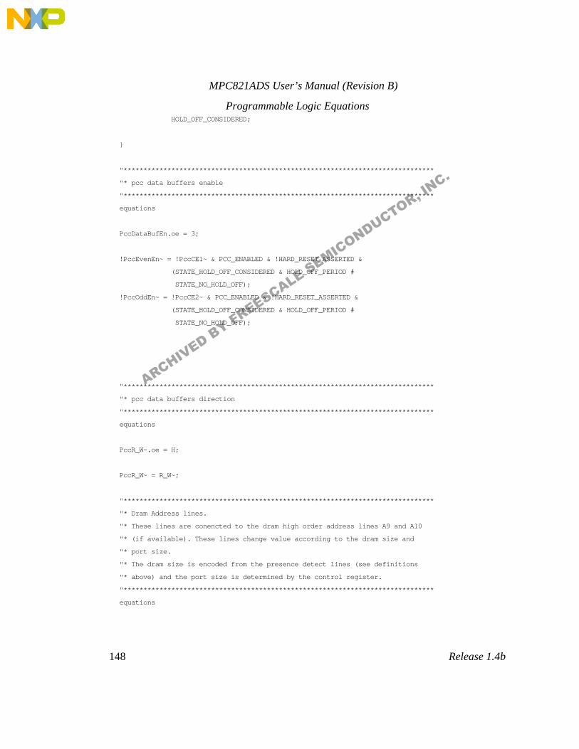
MPC821ADS User’s Manual (Revision B)
148
Release 1.4b
Programmable Logic Equations
HOLD_OFF_CONSIDERED;
"******************************************************************************
"* pcc data buffers enable
"******************************************************************************
equations
PccDataBufEn.oe = 3;
!PccEvenEn~ = !PccCE1~ & PCC_ENABLED & !HARD_RESET_ASSERTED &
(STATE_HOLD_OFF_CONSIDERED & HOLD_OFF_PERIOD #
STATE_NO_HOLD_OFF);
!PccOddEn~ = !PccCE2~ & PCC_ENABLED & !HARD_RESET_ASSERTED &
(STATE_HOLD_OFF_CONSIDERED & HOLD_OFF_PERIOD #
STATE_NO_HOLD_OFF);
"******************************************************************************
"* pcc data buffers direction
"******************************************************************************
equations
PccR_W~.oe = H;
PccR_W~ = R_W~;
"******************************************************************************
"* Dram Address lines.
"* These lines are conencted to the dram high order address lines A9 and A10
"* (if available). These lines change value according to the dram size and
"* port size.
"* The dram size is encoded from the presence detect lines (see definitions
"* above) and the port size is determined by the control register.
"******************************************************************************
equations
ARCHIVED BY FREESCALE SEMICONDUCTOR, INC.
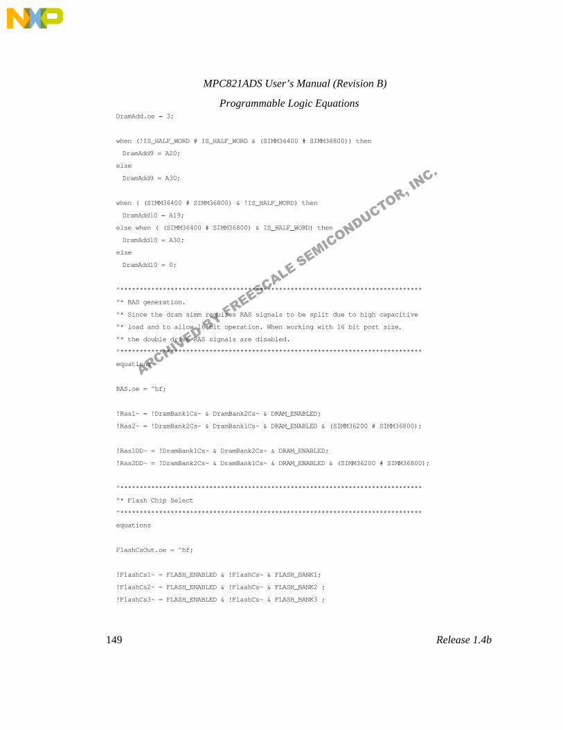
MPC821ADS User’s Manual (Revision B)
149
Release 1.4b
Programmable Logic Equations
DramAdd.oe = 3;
when (!IS_HALF_WORD # IS_HALF_WORD & (SIMM36400 # SIMM36800)) then
DramAdd9 = A20;
else
DramAdd9 = A30;
when ( (SIMM36400 # SIMM36800) & !IS_HALF_WORD) then
DramAdd10 = A19;
else when ( (SIMM36400 # SIMM36800) & IS_HALF_WORD) then
DramAdd10 = A30;
else
DramAdd10 = 0;
"******************************************************************************
"* RAS generation.
"* Since the dram simm requires RAS signals to be split due to high capacitive
"* load and to allow 16 bit operation. When working with 16 bit port size,
"* the double drive RAS signals are disabled.
"******************************************************************************
equations
RAS.oe = hf;
!Ras1~ = !DramBank1Cs~ & DramBank2Cs~ & DRAM_ENABLED;
!Ras2~ = !DramBank2Cs~ & DramBank1Cs~ & DRAM_ENABLED & (SIMM36200 # SIMM36800);
!Ras1DD~ = !DramBank1Cs~ & DramBank2Cs~ & DRAM_ENABLED;
!Ras2DD~ = !DramBank2Cs~ & DramBank1Cs~ & DRAM_ENABLED & (SIMM36200 # SIMM36800);
"******************************************************************************
"* Flash Chip Select
"******************************************************************************
equations
FlashCsOut.oe = hf;
!FlashCs1~ = FLASH_ENABLED & !FlashCs~ & FLASH_BANK1;
!FlashCs2~ = FLASH_ENABLED & !FlashCs~ & FLASH_BANK2 ;
!FlashCs3~ = FLASH_ENABLED & !FlashCs~ & FLASH_BANK3 ;
ARCHIVED BY FREESCALE SEMICONDUCTOR, INC.
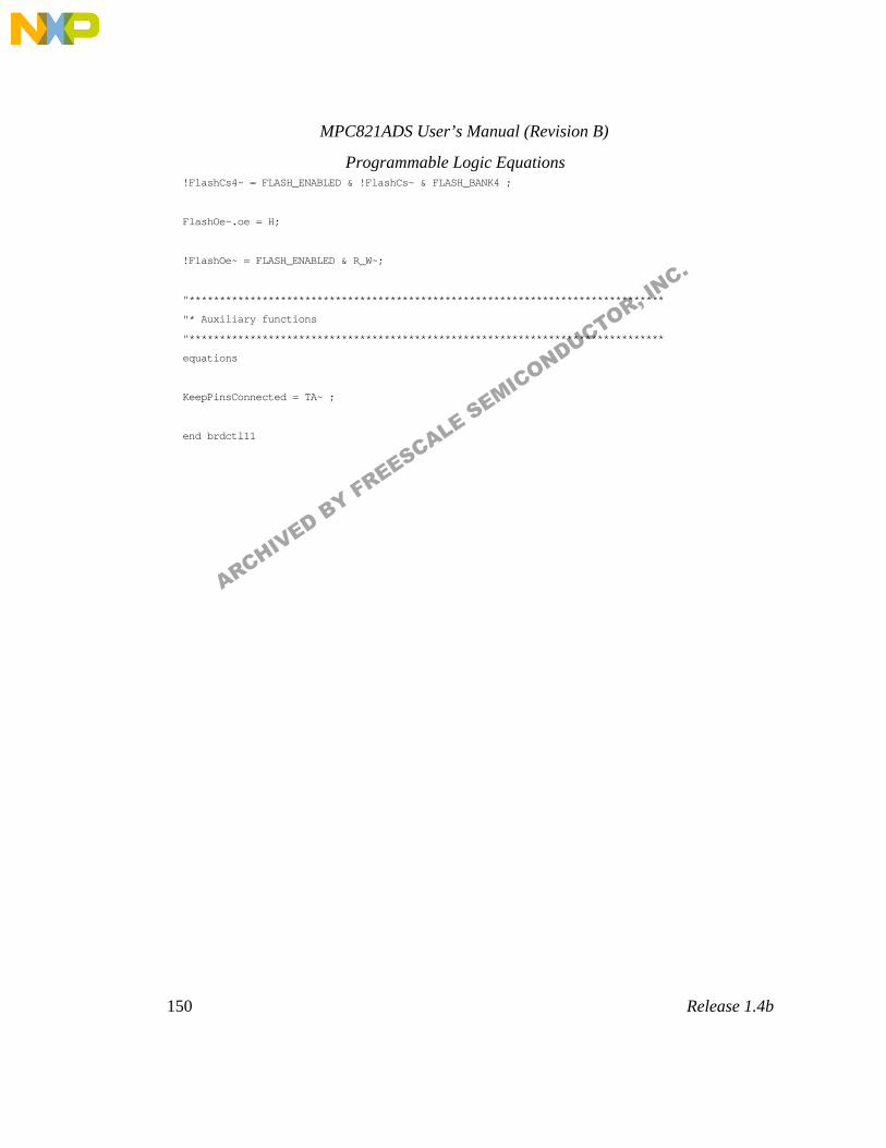
MPC821ADS User’s Manual (Revision B)
150 Release 1.4b
Programmable Logic Equations!FlashCs4~ = FLASH_ENABLED & !FlashCs~ & FLASH_BANK4 ;
FlashOe~.oe = H;
!FlashOe~ = FLASH_ENABLED & R_W~;
"******************************************************************************
"* Auxiliary functions
"******************************************************************************
equations
KeepPinsConnected = TA~ ;
end brdctl11
ARCHIVED BY FREESCALE SEMICONDUCTOR, INC.
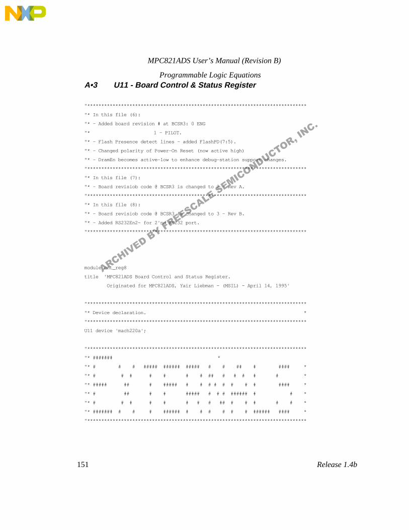
MPC821ADS User’s Manual (Revision B)
151 Release 1.4b
Programmable Logic EquationsA•3 U11 - Board Control & Status Register
"******************************************************************************
"* In this file (6):
"* - Added board revision # at BCSR3: 0 ENG
"* 1 - PILOT.
"* - Flash Presence detect lines - added FlashPD(7:5).
"* - Changed polarity of Power-On Reset (now active high)
"* - DramEn becomes active-low to enhance debug-station support changes.
"******************************************************************************
"* In this file (7):
"* - Board revisiob code @ BCSR3 is changed to 2 - Rev A.
"******************************************************************************
"* In this file (8):
"* - Board revisiob code @ BCSR3 is changed to 3 - Rev B.
"* - Added RS232En2~ for 2'nd RS232 port.
"******************************************************************************
module cnt_reg8
title 'MPC821ADS Board Control and Status Register.
Originated for MPC821ADS, Yair Liebman - (MSIL) - April 14, 1995'
"******************************************************************************
"* Device declaration. *
"******************************************************************************
U11 device 'mach220a';
"******************************************************************************
"* ####### *
"* # # # ##### ###### ##### # # ## # #### *
"* # # # # # # # ## # # # # # *
"* ##### ## # ##### # # # # # # # # #### *
"* # ## # # ##### # # # ###### # # *
"* # # # # # # # # ## # # # # # *
"* ####### # # # ###### # # # # # # ###### #### *
"******************************************************************************
ARCHIVED BY FREESCALE SEMICONDUCTOR, INC.
MPC821ADS User’s Manual (Revision B)
152 Release 1.4b
Programmable Logic Equations"******************************************************************************
"* Pins declaration. *
"******************************************************************************
"* System i/f pins
"******************************************************************************
SYSCLK PIN 15;
RGPORIn PIN 49;
ResetConf~PIN 16;
BrdContRegCs~PIN 50;
TA~ PIN 17;
R_W~ PIN 20;
A28 PIN 51;
A29 PIN 54;
D0 PIN 28;
D1 PIN 29;
D2 PIN 30;
D3 PIN 31;
D4 PIN 36;
D5 PIN 32;
D6 PIN 2;
D7 PIN 26;
D8 PIN 24;
D9 PIN 9;
D10 PIN 6;
D11 PIN 14;
D12 PIN 33;
D13 PIN 37;
D14 PIN 41;
D15 PIN 7;
"******************************************************************************
"* Board Control Pins. Read/Write.
"******************************************************************************
FlashEn~PIN 44 istype 'reg,buffer'; " flash enable.
DramEn~ PIN 55 istype 'reg,buffer'; " dram enable
EthEn~ PIN 46 istype 'reg,buffer'; " ethernet port enable
ARCHIVED BY FREESCALE SEMICONDUCTOR, INC.
MPC821ADS User’s Manual (Revision B)
153 Release 1.4b
Programmable Logic EquationsInfRedEn~PIN 59 istype 'reg,buffer'; " infra-red port enable
FlashCfgEn~PIN 25 istype 'reg,buffer'; " flash configuration enable
CntRegEn~PIN 13 istype 'reg,buffer'; " control register access enable
RS232En1~PIN 48 istype 'reg,buffer'; " RS232 port 1 enable
PccEn~ PIN 40 istype 'reg,buffer'; " PCMCIA port enable
PccVccOn~PIN 39 istype 'reg,buffer'; " PCMCIA operation voltage select
PccVpp0 PIN 5 istype 'reg,buffer'; " PCMCIA programming voltage select
PccVpp1 PIN 3 istype 'reg,buffer'; " PCMCIA programming voltage select
HalfWord~PIN 38 istype 'reg,buffer'; " 32/16 bit dram operation select
RS232En2~PIN 64 istype 'reg,buffer'; " RS232 port 2 enable
"******************************************************************************
"* Board Status Pins. Read only.
"******************************************************************************
FlashPD7PIN 66;
FlashPD6PIN 65;
FlashPD5PIN 67;
FlashPD4PIN 43;
FlashPD3PIN 23;
FlashPD2PIN 22;
FlashPD1PIN 21;" Flash presence detect lines
DramPdEdo~PIN 12;
DramPD4 PIN 10;
DramPD3 PIN 60;
DramPD2 PIN 56;
DramPD1 PIN 45;" Dram SIMM Identification pins
ExtToolI0PIN 57;
ExtToolI1PIN 58;
ExtToolI2PIN 47;
ARCHIVED BY FREESCALE SEMICONDUCTOR, INC.
MPC821ADS User’s Manual (Revision B)
154 Release 1.4b
Programmable Logic EquationsExtToolI3PIN 11;" External Tools Identification pins
PccVppG~PIN 4; " PCMCIA VPP GOOD indication
"******************************************************************************
"* Auxiliary Pins.
"******************************************************************************
"******************************************************************************
"* ### *
"* # # # ##### ###### ##### # # ## # #### *
"* # ## # # # # # ## # # # # # *
"* # # # # # ##### # # # # # # # # #### *
"* # # # # # # ##### # # # ###### # # *
"* # # ## # # # # # ## # # # # # *
"* ### # # # ###### # # # # # # ###### #### *
"******************************************************************************
"* System Hard Reset Configuration.
"******************************************************************************
ERBNODE istype 'reg,buffer'; " External Arbitration
IP~NODE istype 'reg,buffer'; " Interrupt Prefix in MSR
BDISNODE istype 'reg,buffer'; " Boot Disable
RSV2NODE istype 'reg,buffer'; " reserved config bit 2
BPS0,
BPS1NODE istype 'reg,buffer'; " Boot Port Size
RSV6NODE istype 'reg,buffer'; " reserved config bit 6
ISB0,
ISB1NODE istype 'reg,buffer'; " Internal Space Base
DBGC0,
DBGC1NODE istype 'reg,buffer'; " Debug pins Config.
DBPC0,
DBPC1NODE istype 'reg,buffer'; " Debug Port pins Config
RSV13 NODE istype 'reg,buffer'; " reserved config bit 13
RSV14 NODE istype 'reg,buffer'; " reserved config bit 14
RSV15 NODE istype 'reg,buffer'; " reserved config bit 15
DataOeNODE istype 'com';" data bus output enable on read.
ARCHIVED BY FREESCALE SEMICONDUCTOR, INC.
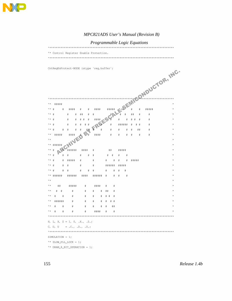
MPC821ADS User’s Manual (Revision B)
155 Release 1.4b
Programmable Logic Equations"******************************************************************************
"* Control Register Enable Protection.
"******************************************************************************
CntRegEnProtect~NODE istype 'reg,buffer';
"******************************************************************************
"* ##### *
"* # # #### # # #### ##### ## # # ##### *
"* # # # ## # # # # # ## # # *
"* # # # # # # #### # # # # # # # *
"* # # # # # # # # ###### # # # # *
"* # # # # # ## # # # # # # ## # *
"* ##### #### # # #### # # # # # # *
"* *
"* ###### *
"* # # ###### #### # ## ##### *
"* # # # # # # # # # # *
"* # # ##### # # # # # # ##### *
"* # # # # # ###### ##### *
"* # # # # # # # # # # *
"* ###### ###### #### ###### # # # # *
"* *
"* ## ##### # #### # # *
"* # # # # # # ## # *
"* # # # # # # # # # *
"* ###### # # # # # # # *
"* # # # # # # # ## *
"* # # # # #### # # *
"******************************************************************************
H, L, X, Z = 1, 0, .X., .Z.;
C, D, U = .C., .D., .U.;
"******************************************************************************
SIMULATION = 1;
"* SLOW_PLL_LOCK = 1;
"* DRAM_8_BIT_OPERATION = 1;
ARCHIVED BY FREESCALE SEMICONDUCTOR, INC.
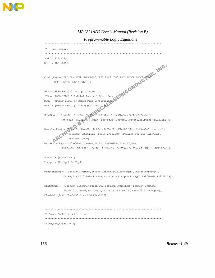
MPC821ADS User’s Manual (Revision B)
156 Release 1.4b
Programmable Logic Equations"******************************************************************************
"* Signal groups
"******************************************************************************
Add = [A28,A29];
Data = [D0..D15];
ConfigReg = [ERB,IP~,RSV2,BDIS,BPS0,BPS1,RSV6,ISB0,ISB1,DBGC0,DBGC1,DBPC0,
DBPC1,RSV13,RSV14,RSV15];
BPS = [BPS0,BPS1];" boot port size
ISB = [ISB0,ISB1];" Initial Internal Space Base
DBGC = [DBGC0,DBGC1];" Debug Pins Configuration
DBPC = [DBPC0,DBPC1];" Debug port location
ContReg = [FlashEn~,DramEn~,EthEn~,InfRedEn~,FlashCfgEn~,CntRegEnProtect~,
CntRegEn~,RS232En1~,PccEn~,PccVccOn~,PccVpp0,PccVpp1,HalfWord~,RS232En2~];
ReadContReg1 = [FlashEn~,DramEn~,EthEn~,InfRedEn~,FlashCfgEn~,CntRegEnProtect~.fb,
CntRegEn~,RS232En1~,PccEn~,PccVccOn~,PccVpp0,PccVpp1,HalfWord~,
RS232En2~,0,0];
DrivenContReg = [FlashEn~,DramEn~,EthEn~,InfRedEn~,FlashCfgEn~,
CntRegEn~,RS232En1~,PccEn~,PccVccOn~,PccVpp0,PccVpp1,HalfWord~,RS232En2~];
PccVcc = [PccVccOn~];
PccVpp = [PccVpp0,PccVpp1];
WideContReg = [FlashEn~,DramEn~,EthEn~,InfRedEn~,FlashCfgEn~,CntRegEnProtect~,
CntRegEn~,RS232En1~,PccEn~,PccVccOn~,PccVpp0,PccVpp1,HalfWord~,RS232En2~];
StatRegIn = [FlashPD4,FlashPD3,FlashPD2,FlashPD1,DramPdEdo~,DramPD4,DramPD3,
DramPD2,DramPD1,ExtToolI0,ExtToolI1,ExtToolI2,ExtToolI3,PccVppG~];
FlashPdHigh = [FlashPD7,FlashPD6,FlashPD5];
"******************************************************************************
"* Power On Reset definitions
"******************************************************************************
FLASH_CFG_ENABLE = 0;
ARCHIVED BY FREESCALE SEMICONDUCTOR, INC.
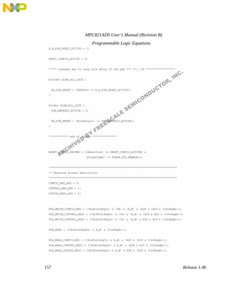
MPC821ADS User’s Manual (Revision B)
157 Release 1.4b
Programmable Logic EquationsK_A_PON_RESET_ACTIVE = 1;
RESET_CONFIG_ACTIVE = 0;
"**** changed due to long lock delay of the pda *** 17,7,95 ******************
@ifndef SLOW_PLL_LOCK
KA_PON_RESET = (RGPORIn == K_A_PON_RESET_ACTIVE);
@ifdef SLOW_PLL_LOCK
PON_DEFAULT_ACTIVE = 0;
KA_PON_RESET = (PonDefault~ == PON_DEFAULT_ACTIVE);
"*********** end of change ***************
RESET_CONFIG_DRIVEN = ((ResetConf~ == RESET_CONFIG_ACTIVE) &
(FlashCfgEn~ != FLASH_CFG_ENABLE));
"******************************************************************************
"* Register Access definitions
"******************************************************************************
CONFIG_REG_ADD = 0;
CONTROL_REG_ADD = 1;
STATUS_REG1_ADD = 2;
PDA_WRITE_CONFIG_REG = (!BrdContRegCs~ & !TA~ & !R_W~ & !A28 & !A29 & !CntRegEn~);
PDA_WRITE_CONTROL_REG1 = (!BrdContRegCs~ & !TA~ & !R_W~ & !A28 & A29 & !CntRegEn~);
PDA_WRITE_CONTROL_REG2 = (!BrdContRegCs~ & !TA~ & !R_W~ & A28 & A29 & !CntRegEn~);
PDA_READ = (!BrdContRegCs~ & R_W~ & !CntRegEn~);
PDA_READ_CONFIG_REG = (!BrdContRegCs~ & R_W~ & !A28 & !A29 & !CntRegEn~);
PDA_READ_CONTROL_REG1 = (!BrdContRegCs~ & R_W~ & !A28 & A29 & !CntRegEn~);
PDA_READ_STATUS_REG1 = (!BrdContRegCs~ & R_W~ & A28 & !A29 & !CntRegEn~);
ARCHIVED BY FREESCALE SEMICONDUCTOR, INC.
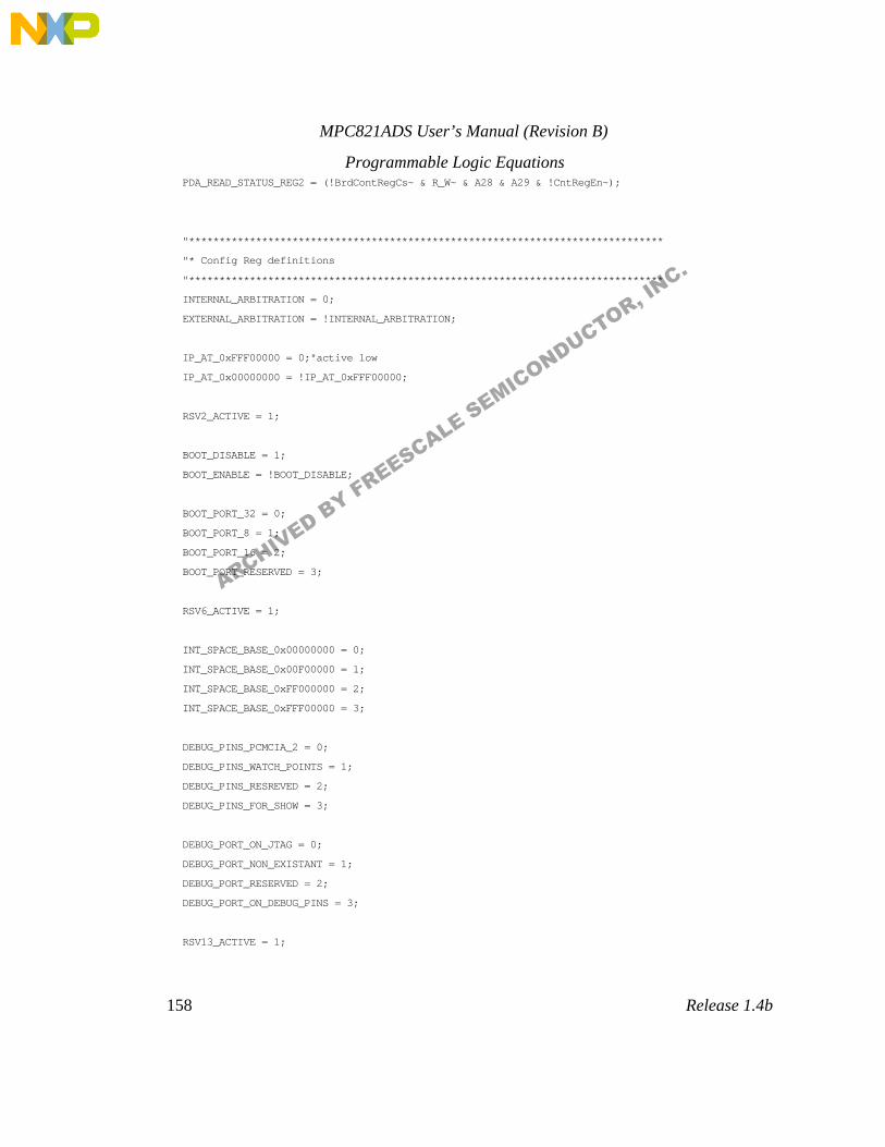
MPC821ADS User’s Manual (Revision B)
158 Release 1.4b
Programmable Logic EquationsPDA_READ_STATUS_REG2 = (!BrdContRegCs~ & R_W~ & A28 & A29 & !CntRegEn~);
"******************************************************************************
"* Config Reg definitions
"******************************************************************************
INTERNAL_ARBITRATION = 0;
EXTERNAL_ARBITRATION = !INTERNAL_ARBITRATION;
IP_AT_0xFFF00000 = 0;"active low
IP_AT_0x00000000 = !IP_AT_0xFFF00000;
RSV2_ACTIVE = 1;
BOOT_DISABLE = 1;
BOOT_ENABLE = !BOOT_DISABLE;
BOOT_PORT_32 = 0;
BOOT_PORT_8 = 1;
BOOT_PORT_16 = 2;
BOOT_PORT_RESERVED = 3;
RSV6_ACTIVE = 1;
INT_SPACE_BASE_0x00000000 = 0;
INT_SPACE_BASE_0x00F00000 = 1;
INT_SPACE_BASE_0xFF000000 = 2;
INT_SPACE_BASE_0xFFF00000 = 3;
DEBUG_PINS_PCMCIA_2 = 0;
DEBUG_PINS_WATCH_POINTS = 1;
DEBUG_PINS_RESREVED = 2;
DEBUG_PINS_FOR_SHOW = 3;
DEBUG_PORT_ON_JTAG = 0;
DEBUG_PORT_NON_EXISTANT = 1;
DEBUG_PORT_RESERVED = 2;
DEBUG_PORT_ON_DEBUG_PINS = 3;
RSV13_ACTIVE = 1;
ARCHIVED BY FREESCALE SEMICONDUCTOR, INC.
MPC821ADS User’s Manual (Revision B)
159 Release 1.4b
Programmable Logic EquationsRSV14_ACTIVE = 1;
RSV15_ACTIVE = 1;
"***********************************************
"******* Power On Defaults Assignments *********
"***********************************************
ERB_PON_DEFAULT = INTERNAL_ARBITRATION;
IP~_PON_DEFAULT = IP_AT_0x00000000;
RSV2_PON_DEFAULT = !RSV2_ACTIVE;
BDIS_PON_DEFAULT = BOOT_ENABLE;
BPS_PON_DEFAULT = BOOT_PORT_32;
RSV6_PON_DEFAULT = !RSV6_ACTIVE;
ISB_PON_DEFAULT = INT_SPACE_BASE_0xFF000000;
DBGC_PON_DEFAULT = DEBUG_PINS_FOR_SHOW;
DBPC_PON_DEFAULT = DEBUG_PORT_ON_JTAG;
RSV13_PON_DEFAULT = !RSV13_ACTIVE;
RSV14_PON_DEFAULT = !RSV14_ACTIVE;
RSV15_PON_DEFAULT = !RSV15_ACTIVE;
"*******************************************
"******* Data Bits Assignments *************
"*******************************************
ARCHIVED BY FREESCALE SEMICONDUCTOR, INC.
MPC821ADS User’s Manual (Revision B)
160 Release 1.4b
Programmable Logic Equations
ERB_DATA_BIT = [D0];
IP~_DATA_BIT = [D1];
RSV2_DATA_BIT = [D2];
BDIS_DATA_BIT = [D3];
BPS_DATA_BIT = [D4,D5];
RSV6_DATA_BIT = [D6];
ISB_DATA_BIT = [D7,D8];
DBGC_DATA_BIT = [D9,D10];
DBPC_DATA_BIT = [D11,D12];
RSV13_DATA_BIT = [D13];
RSV14_DATA_BIT = [D14];
RSV15_DATA_BIT = [D15];
"******************************************************************************
"* Control Register 1 definitions.
"******************************************************************************
HALF_WORD = 0;
ETH_ENABLED = 0;
DRAM_ENABLED = 0;
ETH_LOOP = 1;
TPSQEL = 0;
TP_FULL_DUP = 0;
CONT_REG_ENABLE = 0;
RS232_ENABLE_1 = 0;
RS232_ENABLE_2 = 0;
PCC_ENABLE = 0;
PCC_VCC_ON = 0;
PCC_VCC_OFF = !PCC_VCC_ON;
ARCHIVED BY FREESCALE SEMICONDUCTOR, INC.
MPC821ADS User’s Manual (Revision B)
161 Release 1.4b
Programmable Logic Equations" PCC_VPP_0 = 0;
" PCC_VPP_12 = 2;
" PCC_VPP_5 = 1;
" PCC_VPP_TS = 3;
PCC_VPP0 = 1;
PCC_VPP1 = 1;
FLASH_ENABLED = 0;
INF_RED_ENABLE = 0;
"* FLASH_CFG_ENABLE = 0; needed to be defined ealier
DRAM_5V = 0;
DRAM_3V = !DRAM_5V;
CNT_REG_EN_PROTECT = 0; " inadvertant write protect
"***********************************************
"******* Power On Defaults Assignments *********
"***********************************************
@ifdef DRAM_8_BIT_OPERATION
HALF_WORD_PON_DEFAULT = HALF_WORD;
@ifndef DRAM_8_BIT_OPERATION
HALF_WORD_PON_DEFAULT = !HALF_WORD;
ETH_ENABLE_PON_DEFAULT = !ETH_ENABLED;
DRAM_ENABLE_PON_DEFAULT = DRAM_ENABLED;
CONT_REG_ENABLE_PON_DEFAULT = CONT_REG_ENABLE;
RS232_ENABLE_1_PON_DEFAULT = !RS232_ENABLE_1;
RS232_ENABLE_2_PON_DEFAULT = !RS232_ENABLE_2;
ARCHIVED BY FREESCALE SEMICONDUCTOR, INC.
MPC821ADS User’s Manual (Revision B)
162 Release 1.4b
Programmable Logic Equations
PCC_ENABLE_PON_DEFAULT = !PCC_ENABLE;
PCC_VCC_PON_DEFAULT = PCC_VCC_OFF;
PCC_VPP0_PON_DEFAULT = PCC_VPP0;
PCC_VPP1_PON_DEFAULT = PCC_VPP1; " T.S. as default
FLASH_ENABLE_PON_DEFAULT = FLASH_ENABLED;
INF_RED_ENABLE_PON_DEFAULT = !INF_RED_ENABLE;
FLASH_CFG_ENABLE_PON_DEFAULT = !FLASH_CFG_ENABLE;
CNT_REG_EN_PROTECT_PON_DEFAULT = CNT_REG_EN_PROTECT;
"*******************************************
"******* Data Bits Assignments *************
"*******************************************
FLASH_ENABLE_DATA_BIT = [D0];
DRAM_ENABLE_DATA_BIT = [D1];
ETH_ENABLE_DATA_BIT = [D2];
INF_RED_ENABLE_DATA_BIT = [D3];
FLASH_CFG_ENABLE_DATA_BIT = [D4];
CNT_REG_EN_PROTECT_DATA_BIT = [D5];
CONT_REG_ENABLE_DATA_BIT = [D6];
RS232_ENABLE_1_DATA_BIT = [D7];
PCC_ENABLE_DATA_BIT = [D8];
PCC_VCC_DATA_BIT = [D9];
PCC_VPP0_DATA_BIT = [D10];
PCC_VPP1_DATA_BIT = [D11];
HALF_WORD_DATA_BIT = [D12];
RS232_ENABLE_2_DATA_BIT = [D13];
"******************************************************************************
"* Control Register 2 definitions.
"******************************************************************************
ARCHIVED BY FREESCALE SEMICONDUCTOR, INC.
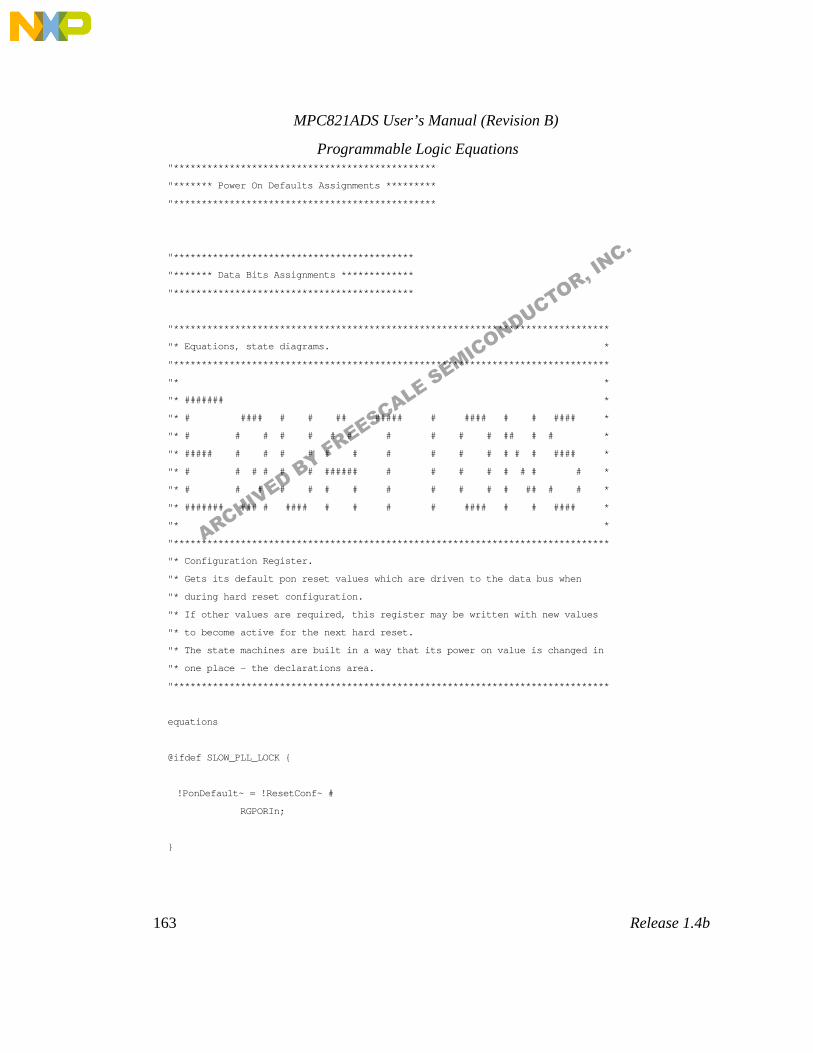
MPC821ADS User’s Manual (Revision B)
163 Release 1.4b
Programmable Logic Equations"***********************************************
"******* Power On Defaults Assignments *********
"***********************************************
"*******************************************
"******* Data Bits Assignments *************
"*******************************************
"******************************************************************************
"* Equations, state diagrams. *
"******************************************************************************
"* *
"* ####### *
"* # #### # # ## ##### # #### # # #### *
"* # # # # # # # # # # # ## # # *
"* ##### # # # # # # # # # # # # # #### *
"* # # # # # # ###### # # # # # # # # *
"* # # # # # # # # # # # # ## # # *
"* ####### ### # #### # # # # #### # # #### *
"* *
"******************************************************************************
"* Configuration Register.
"* Gets its default pon reset values which are driven to the data bus when
"* during hard reset configuration.
"* If other values are required, this register may be written with new values
"* to become active for the next hard reset.
"* The state machines are built in a way that its power on value is changed in
"* one place - the declarations area.
"******************************************************************************
equations
@ifdef SLOW_PLL_LOCK
!PonDefault~ = !ResetConf~ #
RGPORIn;
ARCHIVED BY FREESCALE SEMICONDUCTOR, INC.
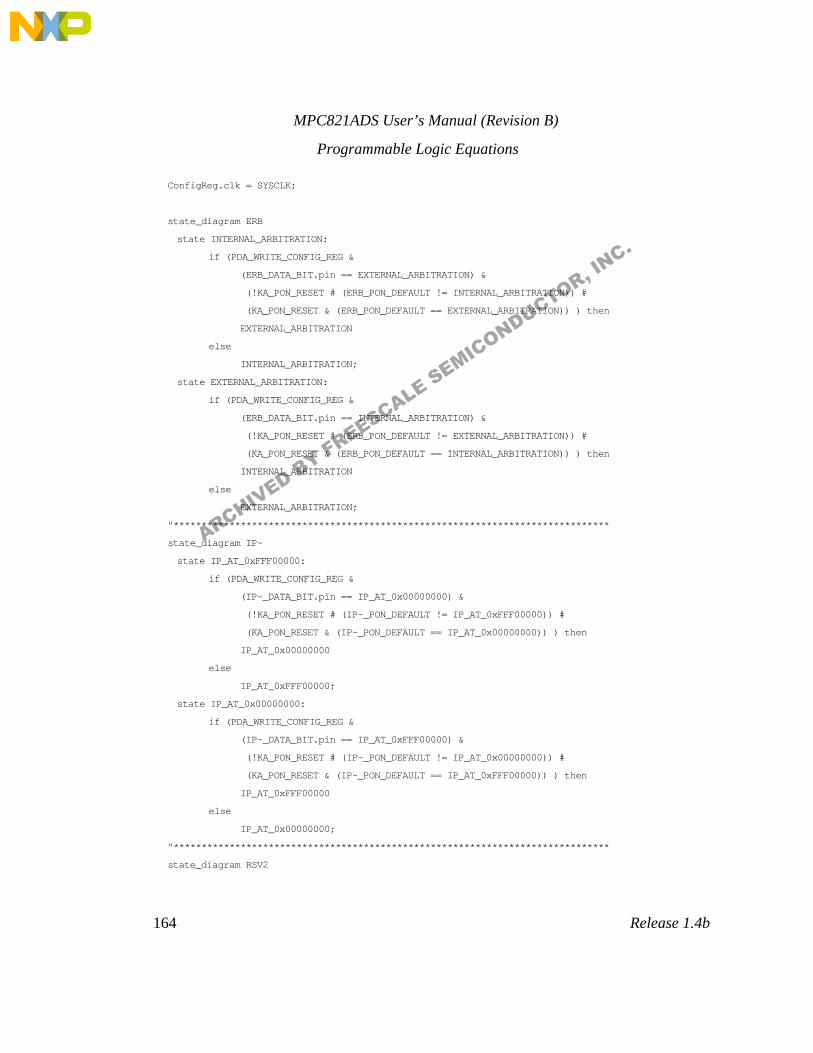
MPC821ADS User’s Manual (Revision B)
164 Release 1.4b
Programmable Logic Equations
ConfigReg.clk = SYSCLK;
state_diagram ERB
state INTERNAL_ARBITRATION:
if (PDA_WRITE_CONFIG_REG &
(ERB_DATA_BIT.pin == EXTERNAL_ARBITRATION) &
(!KA_PON_RESET # (ERB_PON_DEFAULT != INTERNAL_ARBITRATION)) #
(KA_PON_RESET & (ERB_PON_DEFAULT == EXTERNAL_ARBITRATION)) ) then
EXTERNAL_ARBITRATION
else
INTERNAL_ARBITRATION;
state EXTERNAL_ARBITRATION:
if (PDA_WRITE_CONFIG_REG &
(ERB_DATA_BIT.pin == INTERNAL_ARBITRATION) &
(!KA_PON_RESET # (ERB_PON_DEFAULT != EXTERNAL_ARBITRATION)) #
(KA_PON_RESET & (ERB_PON_DEFAULT == INTERNAL_ARBITRATION)) ) then
INTERNAL_ARBITRATION
else
EXTERNAL_ARBITRATION;
"******************************************************************************
state_diagram IP~
state IP_AT_0xFFF00000:
if (PDA_WRITE_CONFIG_REG &
(IP~_DATA_BIT.pin == IP_AT_0x00000000) &
(!KA_PON_RESET # (IP~_PON_DEFAULT != IP_AT_0xFFF00000)) #
(KA_PON_RESET & (IP~_PON_DEFAULT == IP_AT_0x00000000)) ) then
IP_AT_0x00000000
else
IP_AT_0xFFF00000;
state IP_AT_0x00000000:
if (PDA_WRITE_CONFIG_REG &
(IP~_DATA_BIT.pin == IP_AT_0xFFF00000) &
(!KA_PON_RESET # (IP~_PON_DEFAULT != IP_AT_0x00000000)) #
(KA_PON_RESET & (IP~_PON_DEFAULT == IP_AT_0xFFF00000)) ) then
IP_AT_0xFFF00000
else
IP_AT_0x00000000;
"******************************************************************************
state_diagram RSV2
ARCHIVED BY FREESCALE SEMICONDUCTOR, INC.
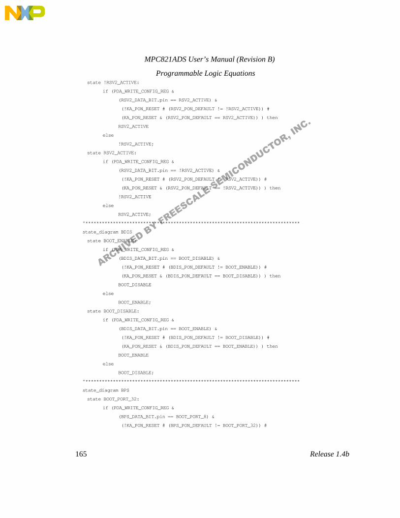
MPC821ADS User’s Manual (Revision B)
165 Release 1.4b
Programmable Logic Equationsstate !RSV2_ACTIVE:
if (PDA_WRITE_CONFIG_REG &
(RSV2_DATA_BIT.pin == RSV2_ACTIVE) &
(!KA_PON_RESET # (RSV2_PON_DEFAULT != !RSV2_ACTIVE)) #
(KA_PON_RESET & (RSV2_PON_DEFAULT == RSV2_ACTIVE)) ) then
RSV2_ACTIVE
else
!RSV2_ACTIVE;
state RSV2_ACTIVE:
if (PDA_WRITE_CONFIG_REG &
(RSV2_DATA_BIT.pin == !RSV2_ACTIVE) &
(!KA_PON_RESET # (RSV2_PON_DEFAULT != RSV2_ACTIVE)) #
(KA_PON_RESET & (RSV2_PON_DEFAULT == !RSV2_ACTIVE)) ) then
!RSV2_ACTIVE
else
RSV2_ACTIVE;
"******************************************************************************
state_diagram BDIS
state BOOT_ENABLE:
if (PDA_WRITE_CONFIG_REG &
(BDIS_DATA_BIT.pin == BOOT_DISABLE) &
(!KA_PON_RESET # (BDIS_PON_DEFAULT != BOOT_ENABLE)) #
(KA_PON_RESET & (BDIS_PON_DEFAULT == BOOT_DISABLE)) ) then
BOOT_DISABLE
else
BOOT_ENABLE;
state BOOT_DISABLE:
if (PDA_WRITE_CONFIG_REG &
(BDIS_DATA_BIT.pin == BOOT_ENABLE) &
(!KA_PON_RESET # (BDIS_PON_DEFAULT != BOOT_DISABLE)) #
(KA_PON_RESET & (BDIS_PON_DEFAULT == BOOT_ENABLE)) ) then
BOOT_ENABLE
else
BOOT_DISABLE;
"******************************************************************************
state_diagram BPS
state BOOT_PORT_32:
if (PDA_WRITE_CONFIG_REG &
(BPS_DATA_BIT.pin == BOOT_PORT_8) &
(!KA_PON_RESET # (BPS_PON_DEFAULT != BOOT_PORT_32)) #
ARCHIVED BY FREESCALE SEMICONDUCTOR, INC.
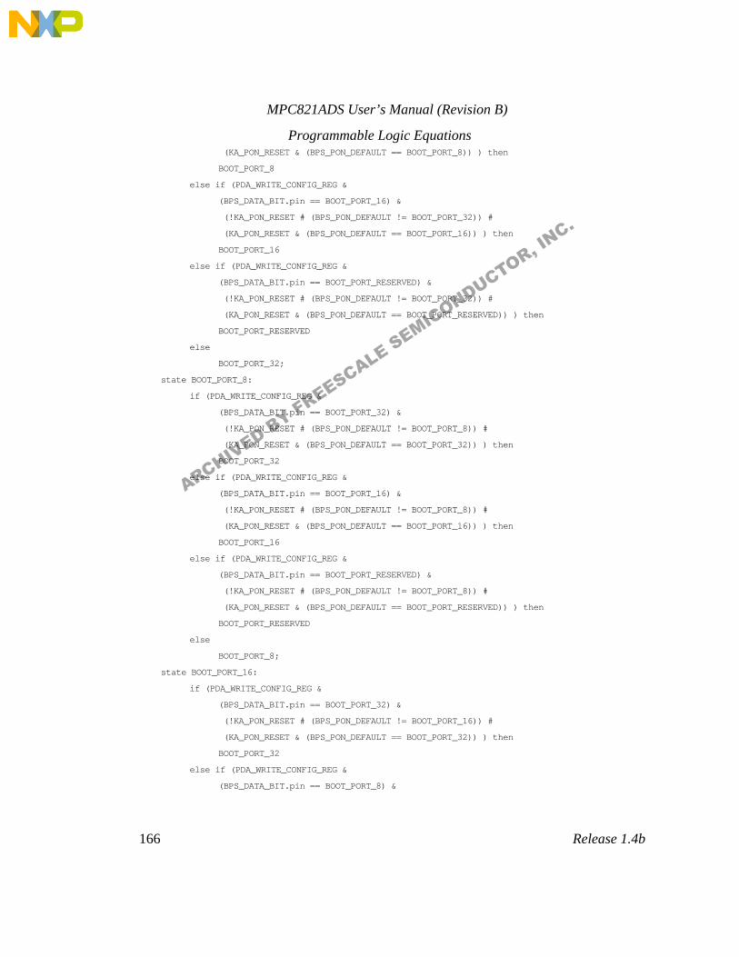
MPC821ADS User’s Manual (Revision B)
166 Release 1.4b
Programmable Logic Equations (KA_PON_RESET & (BPS_PON_DEFAULT == BOOT_PORT_8)) ) then
BOOT_PORT_8
else if (PDA_WRITE_CONFIG_REG &
(BPS_DATA_BIT.pin == BOOT_PORT_16) &
(!KA_PON_RESET # (BPS_PON_DEFAULT != BOOT_PORT_32)) #
(KA_PON_RESET & (BPS_PON_DEFAULT == BOOT_PORT_16)) ) then
BOOT_PORT_16
else if (PDA_WRITE_CONFIG_REG &
(BPS_DATA_BIT.pin == BOOT_PORT_RESERVED) &
(!KA_PON_RESET # (BPS_PON_DEFAULT != BOOT_PORT_32)) #
(KA_PON_RESET & (BPS_PON_DEFAULT == BOOT_PORT_RESERVED)) ) then
BOOT_PORT_RESERVED
else
BOOT_PORT_32;
state BOOT_PORT_8:
if (PDA_WRITE_CONFIG_REG &
(BPS_DATA_BIT.pin == BOOT_PORT_32) &
(!KA_PON_RESET # (BPS_PON_DEFAULT != BOOT_PORT_8)) #
(KA_PON_RESET & (BPS_PON_DEFAULT == BOOT_PORT_32)) ) then
BOOT_PORT_32
else if (PDA_WRITE_CONFIG_REG &
(BPS_DATA_BIT.pin == BOOT_PORT_16) &
(!KA_PON_RESET # (BPS_PON_DEFAULT != BOOT_PORT_8)) #
(KA_PON_RESET & (BPS_PON_DEFAULT == BOOT_PORT_16)) ) then
BOOT_PORT_16
else if (PDA_WRITE_CONFIG_REG &
(BPS_DATA_BIT.pin == BOOT_PORT_RESERVED) &
(!KA_PON_RESET # (BPS_PON_DEFAULT != BOOT_PORT_8)) #
(KA_PON_RESET & (BPS_PON_DEFAULT == BOOT_PORT_RESERVED)) ) then
BOOT_PORT_RESERVED
else
BOOT_PORT_8;
state BOOT_PORT_16:
if (PDA_WRITE_CONFIG_REG &
(BPS_DATA_BIT.pin == BOOT_PORT_32) &
(!KA_PON_RESET # (BPS_PON_DEFAULT != BOOT_PORT_16)) #
(KA_PON_RESET & (BPS_PON_DEFAULT == BOOT_PORT_32)) ) then
BOOT_PORT_32
else if (PDA_WRITE_CONFIG_REG &
(BPS_DATA_BIT.pin == BOOT_PORT_8) &
ARCHIVED BY FREESCALE SEMICONDUCTOR, INC.
MPC821ADS User’s Manual (Revision B)
167 Release 1.4b
Programmable Logic Equations (!KA_PON_RESET # (BPS_PON_DEFAULT != BOOT_PORT_16)) #
(KA_PON_RESET & (BPS_PON_DEFAULT == BOOT_PORT_8)) ) then
BOOT_PORT_8
else if (PDA_WRITE_CONFIG_REG &
(BPS_DATA_BIT.pin == BOOT_PORT_RESERVED) &
(!KA_PON_RESET # (BPS_PON_DEFAULT != BOOT_PORT_16)) #
(KA_PON_RESET & (BPS_PON_DEFAULT == BOOT_PORT_RESERVED)) ) then
BOOT_PORT_RESERVED
else
BOOT_PORT_16;
state BOOT_PORT_RESERVED:
if (PDA_WRITE_CONFIG_REG &
(BPS_DATA_BIT.pin == BOOT_PORT_32) &
(!KA_PON_RESET # (BPS_PON_DEFAULT != BOOT_PORT_RESERVED)) #
(KA_PON_RESET & (BPS_PON_DEFAULT == BOOT_PORT_32)) ) then
BOOT_PORT_32
else if (PDA_WRITE_CONFIG_REG &
(BPS_DATA_BIT.pin == BOOT_PORT_16) &
(!KA_PON_RESET # (BPS_PON_DEFAULT != BOOT_PORT_RESERVED)) #
(KA_PON_RESET & (BPS_PON_DEFAULT == BOOT_PORT_16)) ) then
BOOT_PORT_16
else if (PDA_WRITE_CONFIG_REG &
(BPS_DATA_BIT.pin == BOOT_PORT_8) &
(!KA_PON_RESET # (BPS_PON_DEFAULT != BOOT_PORT_RESERVED)) #
(KA_PON_RESET & (BPS_PON_DEFAULT == BOOT_PORT_8)) ) then
BOOT_PORT_8
else
BOOT_PORT_RESERVED;
"******************************************************************************
state_diagram RSV6
state !RSV6_ACTIVE:
if (PDA_WRITE_CONFIG_REG &
(RSV6_DATA_BIT.pin == RSV6_ACTIVE) &
(!KA_PON_RESET # (RSV6_PON_DEFAULT != !RSV6_ACTIVE)) #
(KA_PON_RESET & (RSV6_PON_DEFAULT == RSV6_ACTIVE)) ) then
RSV6_ACTIVE
else
!RSV6_ACTIVE;
state RSV2_ACTIVE:
if (PDA_WRITE_CONFIG_REG &
ARCHIVED BY FREESCALE SEMICONDUCTOR, INC.
MPC821ADS User’s Manual (Revision B)
168 Release 1.4b
Programmable Logic Equations(RSV6_DATA_BIT.pin == !RSV6_ACTIVE) &
(!KA_PON_RESET # (RSV6_PON_DEFAULT != RSV6_ACTIVE)) #
(KA_PON_RESET & (RSV6_PON_DEFAULT == !RSV6_ACTIVE)) ) then
!RSV6_ACTIVE
else
RSV6_ACTIVE;
"******************************************************************************
state_diagram ISB
state INT_SPACE_BASE_0x00000000:
if (PDA_WRITE_CONFIG_REG &
(ISB_DATA_BIT.pin == INT_SPACE_BASE_0x00F00000) &
(!KA_PON_RESET # (ISB_PON_DEFAULT != INT_SPACE_BASE_0x00000000)) #
(KA_PON_RESET & (ISB_PON_DEFAULT == INT_SPACE_BASE_0x00F00000)) ) then
INT_SPACE_BASE_0x00F00000
else if (PDA_WRITE_CONFIG_REG &
(ISB_DATA_BIT.pin == INT_SPACE_BASE_0xFF000000) &
(!KA_PON_RESET # (ISB_PON_DEFAULT != INT_SPACE_BASE_0x00000000)) #
(KA_PON_RESET & (ISB_PON_DEFAULT == INT_SPACE_BASE_0xFF000000)) ) then
INT_SPACE_BASE_0xFF000000
else if (PDA_WRITE_CONFIG_REG &
(ISB_DATA_BIT.pin == INT_SPACE_BASE_0xFFF00000) &
(!KA_PON_RESET # (ISB_PON_DEFAULT != INT_SPACE_BASE_0x00000000)) #
(KA_PON_RESET & (ISB_PON_DEFAULT == INT_SPACE_BASE_0xFFF00000)) ) then
INT_SPACE_BASE_0xFFF00000
else
INT_SPACE_BASE_0x00000000;
state INT_SPACE_BASE_0x00F00000:
if (PDA_WRITE_CONFIG_REG &
(ISB_DATA_BIT.pin == INT_SPACE_BASE_0x00000000) &
(!KA_PON_RESET # (ISB_PON_DEFAULT != INT_SPACE_BASE_0x00F00000)) #
(KA_PON_RESET & (ISB_PON_DEFAULT == INT_SPACE_BASE_0x00000000)) ) then
INT_SPACE_BASE_0x00000000
else if (PDA_WRITE_CONFIG_REG &
(ISB_DATA_BIT.pin == INT_SPACE_BASE_0xFF000000) &
(!KA_PON_RESET # (ISB_PON_DEFAULT != INT_SPACE_BASE_0x00F00000)) #
(KA_PON_RESET & (ISB_PON_DEFAULT == INT_SPACE_BASE_0xFF000000)) ) then
INT_SPACE_BASE_0xFF000000
else if (PDA_WRITE_CONFIG_REG &
ARCHIVED BY FREESCALE SEMICONDUCTOR, INC.
MPC821ADS User’s Manual (Revision B)
169 Release 1.4b
Programmable Logic Equations(ISB_DATA_BIT.pin == INT_SPACE_BASE_0xFFF00000) &
(!KA_PON_RESET # (ISB_PON_DEFAULT != INT_SPACE_BASE_0x00F00000)) #
(KA_PON_RESET & (ISB_PON_DEFAULT == INT_SPACE_BASE_0xFFF00000)) ) then
INT_SPACE_BASE_0xFFF00000
else
INT_SPACE_BASE_0x00F00000;
state INT_SPACE_BASE_0xFF000000:
if (PDA_WRITE_CONFIG_REG &
(ISB_DATA_BIT.pin == INT_SPACE_BASE_0x00000000) &
(!KA_PON_RESET # (ISB_PON_DEFAULT != INT_SPACE_BASE_0xFF000000)) #
(KA_PON_RESET & (ISB_PON_DEFAULT == INT_SPACE_BASE_0x00000000)) ) then
INT_SPACE_BASE_0x00000000
else if (PDA_WRITE_CONFIG_REG &
(ISB_DATA_BIT.pin == INT_SPACE_BASE_0x00F00000) &
(!KA_PON_RESET # (ISB_PON_DEFAULT != INT_SPACE_BASE_0xFF000000)) #
(KA_PON_RESET & (ISB_PON_DEFAULT == INT_SPACE_BASE_0x00F00000)) ) then
INT_SPACE_BASE_0x00F00000
else if (PDA_WRITE_CONFIG_REG &
(ISB_DATA_BIT.pin == INT_SPACE_BASE_0xFFF00000) &
(!KA_PON_RESET # (ISB_PON_DEFAULT != INT_SPACE_BASE_0xFF000000)) #
(KA_PON_RESET & (ISB_PON_DEFAULT == INT_SPACE_BASE_0xFFF00000)) ) then
INT_SPACE_BASE_0xFFF00000
else
INT_SPACE_BASE_0xFF000000;
state INT_SPACE_BASE_0xFFF00000:
if (PDA_WRITE_CONFIG_REG &
(ISB_DATA_BIT.pin == INT_SPACE_BASE_0x00000000) &
(!KA_PON_RESET # (ISB_PON_DEFAULT != INT_SPACE_BASE_0xFFF00000)) #
(KA_PON_RESET & (ISB_PON_DEFAULT == INT_SPACE_BASE_0x00000000)) ) then
INT_SPACE_BASE_0x00000000
else if (PDA_WRITE_CONFIG_REG &
(ISB_DATA_BIT.pin == INT_SPACE_BASE_0x00F00000) &
(!KA_PON_RESET # (ISB_PON_DEFAULT != INT_SPACE_BASE_0xFFF00000)) #
(KA_PON_RESET & (ISB_PON_DEFAULT == INT_SPACE_BASE_0x00F00000)) ) then
INT_SPACE_BASE_0x00F00000
else if (PDA_WRITE_CONFIG_REG &
(ISB_DATA_BIT.pin == INT_SPACE_BASE_0xFF000000) &
(!KA_PON_RESET # (ISB_PON_DEFAULT != INT_SPACE_BASE_0xFFF00000)) #
ARCHIVED BY FREESCALE SEMICONDUCTOR, INC.
MPC821ADS User’s Manual (Revision B)
170 Release 1.4b
Programmable Logic Equations (KA_PON_RESET & (ISB_PON_DEFAULT == INT_SPACE_BASE_0xFF000000)) ) then
INT_SPACE_BASE_0xFF000000
else
INT_SPACE_BASE_0xFFF00000;
"******************************************************************************
state_diagram DBGC
state DEBUG_PINS_PCMCIA_2:
if (PDA_WRITE_CONFIG_REG &
(DBGC_DATA_BIT.pin == DEBUG_PINS_WATCH_POINTS) &
(!KA_PON_RESET # (DBGC_PON_DEFAULT != DEBUG_PINS_PCMCIA_2)) #
(KA_PON_RESET & (DBGC_PON_DEFAULT == DEBUG_PINS_WATCH_POINTS)) ) then
DEBUG_PINS_WATCH_POINTS
else if (PDA_WRITE_CONFIG_REG &
(DBGC_DATA_BIT.pin == DEBUG_PINS_RESREVED) &
(!KA_PON_RESET # (DBGC_PON_DEFAULT != DEBUG_PINS_PCMCIA_2)) #
(KA_PON_RESET & (DBGC_PON_DEFAULT == DEBUG_PINS_RESREVED)) ) then
DEBUG_PINS_RESREVED
else if (PDA_WRITE_CONFIG_REG &
(DBGC_DATA_BIT.pin == DEBUG_PINS_FOR_SHOW) &
(!KA_PON_RESET # (DBGC_PON_DEFAULT != DEBUG_PINS_PCMCIA_2)) #
(KA_PON_RESET & (DBGC_PON_DEFAULT == DEBUG_PINS_FOR_SHOW)) ) then
DEBUG_PINS_FOR_SHOW
else
DEBUG_PINS_PCMCIA_2;
state DEBUG_PINS_WATCH_POINTS:
if (PDA_WRITE_CONFIG_REG &
(DBGC_DATA_BIT.pin == DEBUG_PINS_PCMCIA_2) &
(!KA_PON_RESET # (DBGC_PON_DEFAULT != DEBUG_PINS_WATCH_POINTS)) #
(KA_PON_RESET & (DBGC_PON_DEFAULT == DEBUG_PINS_PCMCIA_2)) ) then
DEBUG_PINS_PCMCIA_2
else if (PDA_WRITE_CONFIG_REG &
(DBGC_DATA_BIT.pin == DEBUG_PINS_RESREVED) &
(!KA_PON_RESET # (DBGC_PON_DEFAULT != DEBUG_PINS_WATCH_POINTS)) #
(KA_PON_RESET & (DBGC_PON_DEFAULT == DEBUG_PINS_RESREVED)) ) then
DEBUG_PINS_RESREVED
else if (PDA_WRITE_CONFIG_REG &
(DBGC_DATA_BIT.pin == DEBUG_PINS_FOR_SHOW) &
(!KA_PON_RESET # (DBGC_PON_DEFAULT != DEBUG_PINS_WATCH_POINTS)) #
(KA_PON_RESET & (DBGC_PON_DEFAULT == DEBUG_PINS_FOR_SHOW)) ) then
ARCHIVED BY FREESCALE SEMICONDUCTOR, INC.
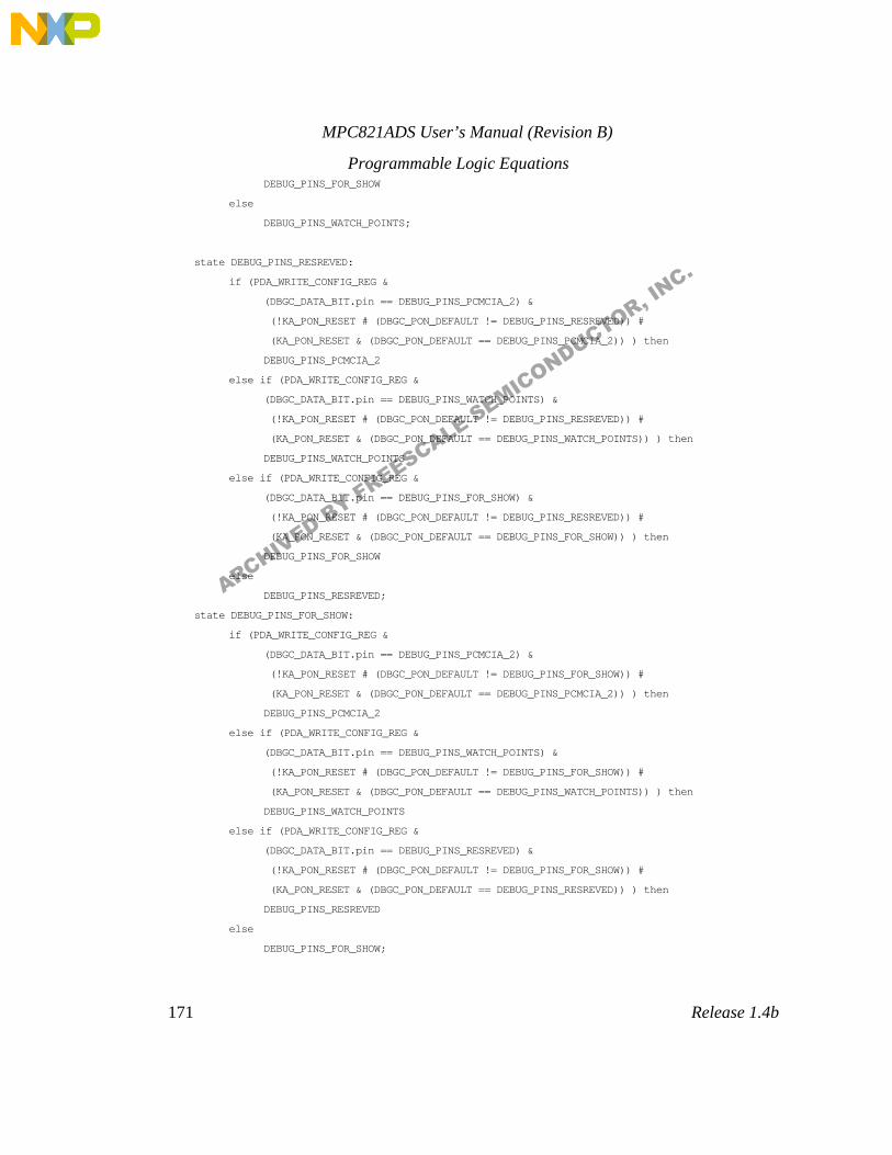
MPC821ADS User’s Manual (Revision B)
171 Release 1.4b
Programmable Logic EquationsDEBUG_PINS_FOR_SHOW
else
DEBUG_PINS_WATCH_POINTS;
state DEBUG_PINS_RESREVED:
if (PDA_WRITE_CONFIG_REG &
(DBGC_DATA_BIT.pin == DEBUG_PINS_PCMCIA_2) &
(!KA_PON_RESET # (DBGC_PON_DEFAULT != DEBUG_PINS_RESREVED)) #
(KA_PON_RESET & (DBGC_PON_DEFAULT == DEBUG_PINS_PCMCIA_2)) ) then
DEBUG_PINS_PCMCIA_2
else if (PDA_WRITE_CONFIG_REG &
(DBGC_DATA_BIT.pin == DEBUG_PINS_WATCH_POINTS) &
(!KA_PON_RESET # (DBGC_PON_DEFAULT != DEBUG_PINS_RESREVED)) #
(KA_PON_RESET & (DBGC_PON_DEFAULT == DEBUG_PINS_WATCH_POINTS)) ) then
DEBUG_PINS_WATCH_POINTS
else if (PDA_WRITE_CONFIG_REG &
(DBGC_DATA_BIT.pin == DEBUG_PINS_FOR_SHOW) &
(!KA_PON_RESET # (DBGC_PON_DEFAULT != DEBUG_PINS_RESREVED)) #
(KA_PON_RESET & (DBGC_PON_DEFAULT == DEBUG_PINS_FOR_SHOW)) ) then
DEBUG_PINS_FOR_SHOW
else
DEBUG_PINS_RESREVED;
state DEBUG_PINS_FOR_SHOW:
if (PDA_WRITE_CONFIG_REG &
(DBGC_DATA_BIT.pin == DEBUG_PINS_PCMCIA_2) &
(!KA_PON_RESET # (DBGC_PON_DEFAULT != DEBUG_PINS_FOR_SHOW)) #
(KA_PON_RESET & (DBGC_PON_DEFAULT == DEBUG_PINS_PCMCIA_2)) ) then
DEBUG_PINS_PCMCIA_2
else if (PDA_WRITE_CONFIG_REG &
(DBGC_DATA_BIT.pin == DEBUG_PINS_WATCH_POINTS) &
(!KA_PON_RESET # (DBGC_PON_DEFAULT != DEBUG_PINS_FOR_SHOW)) #
(KA_PON_RESET & (DBGC_PON_DEFAULT == DEBUG_PINS_WATCH_POINTS)) ) then
DEBUG_PINS_WATCH_POINTS
else if (PDA_WRITE_CONFIG_REG &
(DBGC_DATA_BIT.pin == DEBUG_PINS_RESREVED) &
(!KA_PON_RESET # (DBGC_PON_DEFAULT != DEBUG_PINS_FOR_SHOW)) #
(KA_PON_RESET & (DBGC_PON_DEFAULT == DEBUG_PINS_RESREVED)) ) then
DEBUG_PINS_RESREVED
else
DEBUG_PINS_FOR_SHOW;
ARCHIVED BY FREESCALE SEMICONDUCTOR, INC.
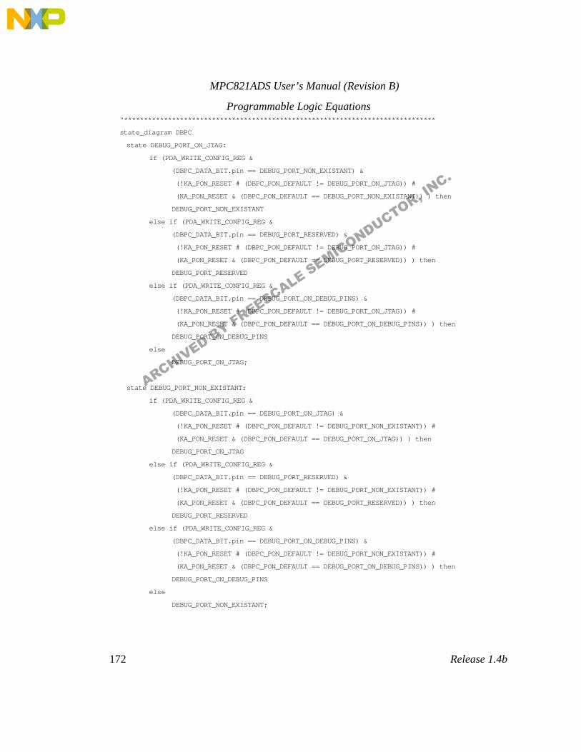
MPC821ADS User’s Manual (Revision B)
172 Release 1.4b
Programmable Logic Equations"******************************************************************************
state_diagram DBPC
state DEBUG_PORT_ON_JTAG:
if (PDA_WRITE_CONFIG_REG &
(DBPC_DATA_BIT.pin == DEBUG_PORT_NON_EXISTANT) &
(!KA_PON_RESET # (DBPC_PON_DEFAULT != DEBUG_PORT_ON_JTAG)) #
(KA_PON_RESET & (DBPC_PON_DEFAULT == DEBUG_PORT_NON_EXISTANT)) ) then
DEBUG_PORT_NON_EXISTANT
else if (PDA_WRITE_CONFIG_REG &
(DBPC_DATA_BIT.pin == DEBUG_PORT_RESERVED) &
(!KA_PON_RESET # (DBPC_PON_DEFAULT != DEBUG_PORT_ON_JTAG)) #
(KA_PON_RESET & (DBPC_PON_DEFAULT == DEBUG_PORT_RESERVED)) ) then
DEBUG_PORT_RESERVED
else if (PDA_WRITE_CONFIG_REG &
(DBPC_DATA_BIT.pin == DEBUG_PORT_ON_DEBUG_PINS) &
(!KA_PON_RESET # (DBPC_PON_DEFAULT != DEBUG_PORT_ON_JTAG)) #
(KA_PON_RESET & (DBPC_PON_DEFAULT == DEBUG_PORT_ON_DEBUG_PINS)) ) then
DEBUG_PORT_ON_DEBUG_PINS
else
DEBUG_PORT_ON_JTAG;
state DEBUG_PORT_NON_EXISTANT:
if (PDA_WRITE_CONFIG_REG &
(DBPC_DATA_BIT.pin == DEBUG_PORT_ON_JTAG) &
(!KA_PON_RESET # (DBPC_PON_DEFAULT != DEBUG_PORT_NON_EXISTANT)) #
(KA_PON_RESET & (DBPC_PON_DEFAULT == DEBUG_PORT_ON_JTAG)) ) then
DEBUG_PORT_ON_JTAG
else if (PDA_WRITE_CONFIG_REG &
(DBPC_DATA_BIT.pin == DEBUG_PORT_RESERVED) &
(!KA_PON_RESET # (DBPC_PON_DEFAULT != DEBUG_PORT_NON_EXISTANT)) #
(KA_PON_RESET & (DBPC_PON_DEFAULT == DEBUG_PORT_RESERVED)) ) then
DEBUG_PORT_RESERVED
else if (PDA_WRITE_CONFIG_REG &
(DBPC_DATA_BIT.pin == DEBUG_PORT_ON_DEBUG_PINS) &
(!KA_PON_RESET # (DBPC_PON_DEFAULT != DEBUG_PORT_NON_EXISTANT)) #
(KA_PON_RESET & (DBPC_PON_DEFAULT == DEBUG_PORT_ON_DEBUG_PINS)) ) then
DEBUG_PORT_ON_DEBUG_PINS
else
DEBUG_PORT_NON_EXISTANT;
ARCHIVED BY FREESCALE SEMICONDUCTOR, INC.
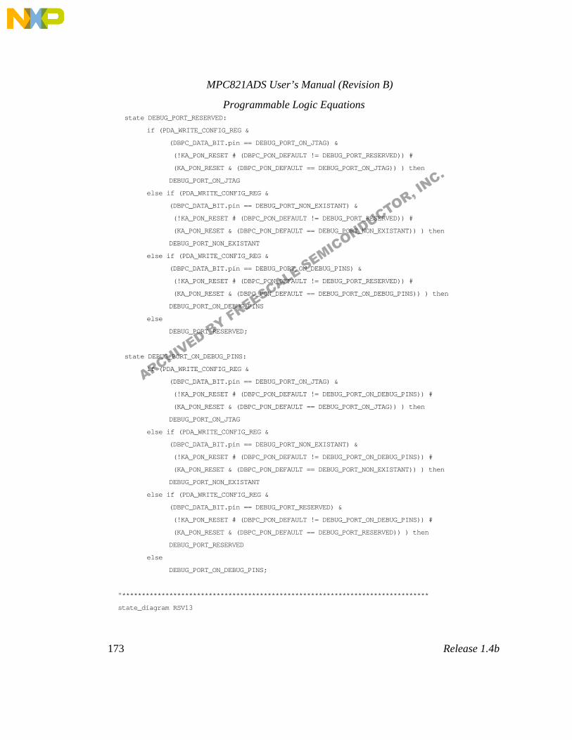
MPC821ADS User’s Manual (Revision B)
173 Release 1.4b
Programmable Logic Equationsstate DEBUG_PORT_RESERVED:
if (PDA_WRITE_CONFIG_REG &
(DBPC_DATA_BIT.pin == DEBUG_PORT_ON_JTAG) &
(!KA_PON_RESET # (DBPC_PON_DEFAULT != DEBUG_PORT_RESERVED)) #
(KA_PON_RESET & (DBPC_PON_DEFAULT == DEBUG_PORT_ON_JTAG)) ) then
DEBUG_PORT_ON_JTAG
else if (PDA_WRITE_CONFIG_REG &
(DBPC_DATA_BIT.pin == DEBUG_PORT_NON_EXISTANT) &
(!KA_PON_RESET # (DBPC_PON_DEFAULT != DEBUG_PORT_RESERVED)) #
(KA_PON_RESET & (DBPC_PON_DEFAULT == DEBUG_PORT_NON_EXISTANT)) ) then
DEBUG_PORT_NON_EXISTANT
else if (PDA_WRITE_CONFIG_REG &
(DBPC_DATA_BIT.pin == DEBUG_PORT_ON_DEBUG_PINS) &
(!KA_PON_RESET # (DBPC_PON_DEFAULT != DEBUG_PORT_RESERVED)) #
(KA_PON_RESET & (DBPC_PON_DEFAULT == DEBUG_PORT_ON_DEBUG_PINS)) ) then
DEBUG_PORT_ON_DEBUG_PINS
else
DEBUG_PORT_RESERVED;
state DEBUG_PORT_ON_DEBUG_PINS:
if (PDA_WRITE_CONFIG_REG &
(DBPC_DATA_BIT.pin == DEBUG_PORT_ON_JTAG) &
(!KA_PON_RESET # (DBPC_PON_DEFAULT != DEBUG_PORT_ON_DEBUG_PINS)) #
(KA_PON_RESET & (DBPC_PON_DEFAULT == DEBUG_PORT_ON_JTAG)) ) then
DEBUG_PORT_ON_JTAG
else if (PDA_WRITE_CONFIG_REG &
(DBPC_DATA_BIT.pin == DEBUG_PORT_NON_EXISTANT) &
(!KA_PON_RESET # (DBPC_PON_DEFAULT != DEBUG_PORT_ON_DEBUG_PINS)) #
(KA_PON_RESET & (DBPC_PON_DEFAULT == DEBUG_PORT_NON_EXISTANT)) ) then
DEBUG_PORT_NON_EXISTANT
else if (PDA_WRITE_CONFIG_REG &
(DBPC_DATA_BIT.pin == DEBUG_PORT_RESERVED) &
(!KA_PON_RESET # (DBPC_PON_DEFAULT != DEBUG_PORT_ON_DEBUG_PINS)) #
(KA_PON_RESET & (DBPC_PON_DEFAULT == DEBUG_PORT_RESERVED)) ) then
DEBUG_PORT_RESERVED
else
DEBUG_PORT_ON_DEBUG_PINS;
"******************************************************************************
state_diagram RSV13
ARCHIVED BY FREESCALE SEMICONDUCTOR, INC.
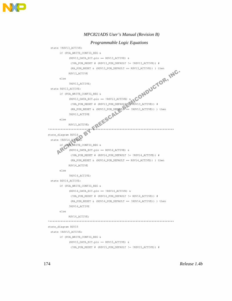
MPC821ADS User’s Manual (Revision B)
174 Release 1.4b
Programmable Logic Equationsstate !RSV13_ACTIVE:
if (PDA_WRITE_CONFIG_REG &
(RSV13_DATA_BIT.pin == RSV13_ACTIVE) &
(!KA_PON_RESET # (RSV13_PON_DEFAULT != !RSV13_ACTIVE)) #
(KA_PON_RESET & (RSV13_PON_DEFAULT == RSV13_ACTIVE)) ) then
RSV13_ACTIVE
else
!RSV13_ACTIVE;
state RSV13_ACTIVE:
if (PDA_WRITE_CONFIG_REG &
(RSV13_DATA_BIT.pin == !RSV13_ACTIVE) &
(!KA_PON_RESET # (RSV13_PON_DEFAULT != RSV13_ACTIVE)) #
(KA_PON_RESET & (RSV13_PON_DEFAULT == !RSV13_ACTIVE)) ) then
!RSV13_ACTIVE
else
RSV13_ACTIVE;
"******************************************************************************
state_diagram RSV14
state !RSV14_ACTIVE:
if (PDA_WRITE_CONFIG_REG &
(RSV14_DATA_BIT.pin == RSV14_ACTIVE) &
(!KA_PON_RESET # (RSV14_PON_DEFAULT != !RSV14_ACTIVE)) #
(KA_PON_RESET & (RSV14_PON_DEFAULT == RSV14_ACTIVE)) ) then
RSV14_ACTIVE
else
!RSV14_ACTIVE;
state RSV14_ACTIVE:
if (PDA_WRITE_CONFIG_REG &
(RSV14_DATA_BIT.pin == !RSV14_ACTIVE) &
(!KA_PON_RESET # (RSV14_PON_DEFAULT != RSV14_ACTIVE)) #
(KA_PON_RESET & (RSV14_PON_DEFAULT == !RSV14_ACTIVE)) ) then
!RSV14_ACTIVE
else
RSV14_ACTIVE;
"******************************************************************************
state_diagram RSV15
state !RSV15_ACTIVE:
if (PDA_WRITE_CONFIG_REG &
(RSV15_DATA_BIT.pin == RSV15_ACTIVE) &
(!KA_PON_RESET # (RSV15_PON_DEFAULT != !RSV15_ACTIVE)) #
ARCHIVED BY FREESCALE SEMICONDUCTOR, INC.
MPC821ADS User’s Manual (Revision B)
175 Release 1.4b
Programmable Logic Equations (KA_PON_RESET & (RSV15_PON_DEFAULT == RSV15_ACTIVE)) ) then
RSV15_ACTIVE
else
!RSV15_ACTIVE;
state RSV15_ACTIVE:
if (PDA_WRITE_CONFIG_REG &
(RSV15_DATA_BIT.pin == !RSV15_ACTIVE) &
(!KA_PON_RESET # (RSV15_PON_DEFAULT != RSV15_ACTIVE)) #
(KA_PON_RESET & (RSV15_PON_DEFAULT == !RSV15_ACTIVE)) ) then
!RSV15_ACTIVE
else
RSV15_ACTIVE;
"******************************************************************************
"* Control Register.
"******************************************************************************
equations
WideContReg.clk = SYSCLK;
DrivenContReg.oe = h1fff;
state_diagram FlashEn~
state FLASH_ENABLED:
if (PDA_WRITE_CONTROL_REG1 &
(FLASH_ENABLE_DATA_BIT.pin == !FLASH_ENABLED) &
(!KA_PON_RESET # (FLASH_ENABLE_PON_DEFAULT != FLASH_ENABLED)) #
(KA_PON_RESET & (FLASH_ENABLE_PON_DEFAULT == !FLASH_ENABLED)) ) then
!FLASH_ENABLED
else
FLASH_ENABLED;
state !FLASH_ENABLED:
if (PDA_WRITE_CONTROL_REG1 &
(FLASH_ENABLE_DATA_BIT.pin == FLASH_ENABLED) &
(!KA_PON_RESET # (FLASH_ENABLE_PON_DEFAULT != !FLASH_ENABLED)) #
(KA_PON_RESET & (FLASH_ENABLE_PON_DEFAULT == FLASH_ENABLED)) ) then
FLASH_ENABLED
else
!FLASH_ENABLED;
"******************************************************************************
state_diagram DramEn~
state DRAM_ENABLED:
ARCHIVED BY FREESCALE SEMICONDUCTOR, INC.
MPC821ADS User’s Manual (Revision B)
176 Release 1.4b
Programmable Logic Equationsif (PDA_WRITE_CONTROL_REG1 &
(DRAM_ENABLE_DATA_BIT.pin == !DRAM_ENABLED) &
(!KA_PON_RESET # (DRAM_ENABLE_PON_DEFAULT != DRAM_ENABLED)) #
(KA_PON_RESET & (DRAM_ENABLE_PON_DEFAULT == !DRAM_ENABLED)) ) then
!DRAM_ENABLED
else
DRAM_ENABLED;
state !DRAM_ENABLED:
if (PDA_WRITE_CONTROL_REG1 &
(DRAM_ENABLE_DATA_BIT.pin == DRAM_ENABLED) &
(!KA_PON_RESET # (DRAM_ENABLE_PON_DEFAULT != !DRAM_ENABLED)) #
(KA_PON_RESET & (DRAM_ENABLE_PON_DEFAULT == DRAM_ENABLED)) ) then
DRAM_ENABLED
else
!DRAM_ENABLED;
"******************************************************************************
state_diagram EthEn~
state ETH_ENABLED:
if (PDA_WRITE_CONTROL_REG1 &
(ETH_ENABLE_DATA_BIT.pin == !ETH_ENABLED) &
(!KA_PON_RESET # (ETH_ENABLE_PON_DEFAULT != ETH_ENABLED)) #
(KA_PON_RESET & (ETH_ENABLE_PON_DEFAULT == !ETH_ENABLED)) ) then
!ETH_ENABLED
else
ETH_ENABLED;
state !ETH_ENABLED:
if (PDA_WRITE_CONTROL_REG1 &
(ETH_ENABLE_DATA_BIT.pin == ETH_ENABLED) &
(!KA_PON_RESET # (ETH_ENABLE_PON_DEFAULT != !ETH_ENABLED)) #
(KA_PON_RESET & (ETH_ENABLE_PON_DEFAULT == ETH_ENABLED)) ) then
ETH_ENABLED
else
!ETH_ENABLED;
"******************************************************************************
state_diagram InfRedEn~
state INF_RED_ENABLE:
if (PDA_WRITE_CONTROL_REG1 &
(INF_RED_ENABLE_DATA_BIT.pin == !INF_RED_ENABLE) &
(!KA_PON_RESET # (INF_RED_ENABLE_PON_DEFAULT != INF_RED_ENABLE)) #
ARCHIVED BY FREESCALE SEMICONDUCTOR, INC.
MPC821ADS User’s Manual (Revision B)
177 Release 1.4b
Programmable Logic Equations (KA_PON_RESET & (INF_RED_ENABLE_PON_DEFAULT == !INF_RED_ENABLE)) ) then
!INF_RED_ENABLE
else
INF_RED_ENABLE;
state !INF_RED_ENABLE:
if (PDA_WRITE_CONTROL_REG1 &
(INF_RED_ENABLE_DATA_BIT.pin == INF_RED_ENABLE) &
(!KA_PON_RESET # (INF_RED_ENABLE_PON_DEFAULT != !INF_RED_ENABLE)) #
(KA_PON_RESET & (INF_RED_ENABLE_PON_DEFAULT == INF_RED_ENABLE)) ) then
INF_RED_ENABLE
else
!INF_RED_ENABLE;
"******************************************************************************
state_diagram FlashCfgEn~
state FLASH_CFG_ENABLE:
if (PDA_WRITE_CONTROL_REG1 &
(FLASH_CFG_ENABLE_DATA_BIT.pin == !FLASH_CFG_ENABLE) &
(!KA_PON_RESET # (FLASH_CFG_ENABLE_PON_DEFAULT != FLASH_CFG_ENABLE)) #
(KA_PON_RESET & (FLASH_CFG_ENABLE_PON_DEFAULT == !FLASH_CFG_ENABLE)) )
then
!FLASH_CFG_ENABLE
else
FLASH_CFG_ENABLE;
state !FLASH_CFG_ENABLE:
if (PDA_WRITE_CONTROL_REG1 &
(FLASH_CFG_ENABLE_DATA_BIT.pin == FLASH_CFG_ENABLE) &
(!KA_PON_RESET # (FLASH_CFG_ENABLE_PON_DEFAULT != !FLASH_CFG_ENABLE)) #
(KA_PON_RESET & (FLASH_CFG_ENABLE_PON_DEFAULT == FLASH_CFG_ENABLE)) ) then
FLASH_CFG_ENABLE
else
!FLASH_CFG_ENABLE;
"******************************************************************************
"* To avoid in advertant write to the Control Register Enable bit, which might
"* result in a need to re-power the board - protection logic is provided.
"* In order of writing the Control Register Enable this bit in the status register
"* must be negated. After any write to the control register, this bit asserts
"* again (to protected mode)
"******************************************************************************
equations
ARCHIVED BY FREESCALE SEMICONDUCTOR, INC.
MPC821ADS User’s Manual (Revision B)
178 Release 1.4b
Programmable Logic EquationsCntRegEnProtect~.clk = SYSCLK;
state_diagram CntRegEnProtect~
state CNT_REG_EN_PROTECT:
if (PDA_WRITE_CONTROL_REG2 &
(CNT_REG_EN_PROTECT_DATA_BIT.pin == !CNT_REG_EN_PROTECT) &
(!KA_PON_RESET # (CNT_REG_EN_PROTECT_PON_DEFAULT != CNT_REG_EN_PROTECT)) #
(KA_PON_RESET & (CNT_REG_EN_PROTECT_PON_DEFAULT == !CNT_REG_EN_PROTECT)))then
!CNT_REG_EN_PROTECT
else
CNT_REG_EN_PROTECT;
state !CNT_REG_EN_PROTECT:
if (PDA_WRITE_CONTROL_REG2 &
(CNT_REG_EN_PROTECT_DATA_BIT.pin == CNT_REG_EN_PROTECT) &
(!KA_PON_RESET # (CNT_REG_EN_PROTECT_PON_DEFAULT != !CNT_REG_EN_PROTECT))#
(KA_PON_RESET & (CNT_REG_EN_PROTECT_PON_DEFAULT == CNT_REG_EN_PROTECT)) #
PDA_WRITE_CONTROL_REG1) then " any write to control reg 1
CNT_REG_EN_PROTECT
else
!CNT_REG_EN_PROTECT;
"******************************************************************************
"* protected by CntRegEnProtect~ to prevent from inadvertant write
"******************************************************************************
state_diagram CntRegEn~
state CONT_REG_ENABLE:
if (PDA_WRITE_CONTROL_REG1 & (CntRegEnProtect~.fb != CNT_REG_EN_PROTECT) &
(CONT_REG_ENABLE_DATA_BIT.pin == !CONT_REG_ENABLE) &
(!KA_PON_RESET # (CONT_REG_ENABLE_PON_DEFAULT != CONT_REG_ENABLE)) #
(KA_PON_RESET & (CONT_REG_ENABLE_PON_DEFAULT == !CONT_REG_ENABLE)) ) then
!CONT_REG_ENABLE
else
CONT_REG_ENABLE;
state !CONT_REG_ENABLE:" in fact not applicable
if (PDA_WRITE_CONTROL_REG1 &
(CONT_REG_ENABLE_DATA_BIT.pin == CONT_REG_ENABLE) &
(!KA_PON_RESET # (CONT_REG_ENABLE_PON_DEFAULT != !CONT_REG_ENABLE)) #
(KA_PON_RESET & (CONT_REG_ENABLE_PON_DEFAULT == CONT_REG_ENABLE)) ) then
CONT_REG_ENABLE
else
ARCHIVED BY FREESCALE SEMICONDUCTOR, INC.
MPC821ADS User’s Manual (Revision B)
179 Release 1.4b
Programmable Logic Equations!CONT_REG_ENABLE;
"******************************************************************************
state_diagram RS232En1~
state RS232_ENABLE_1:
if (PDA_WRITE_CONTROL_REG1 &
(RS232_ENABLE_1_DATA_BIT.pin == !RS232_ENABLE_1) &
(!KA_PON_RESET # (RS232_ENABLE_1_PON_DEFAULT != RS232_ENABLE_1)) #
(KA_PON_RESET & (RS232_ENABLE_1_PON_DEFAULT == !RS232_ENABLE_1)) ) then
!RS232_ENABLE_1
else
RS232_ENABLE_1;
state !RS232_ENABLE_1:
if (PDA_WRITE_CONTROL_REG1 &
(RS232_ENABLE_1_DATA_BIT.pin == RS232_ENABLE_1) &
(!KA_PON_RESET # (RS232_ENABLE_1_PON_DEFAULT != !RS232_ENABLE_1)) #
(KA_PON_RESET & (RS232_ENABLE_1_PON_DEFAULT == RS232_ENABLE_1)) ) then
RS232_ENABLE_1
else
!RS232_ENABLE_1;
"******************************************************************************
state_diagram PccEn~
state PCC_ENABLE:
if (PDA_WRITE_CONTROL_REG1 &
(PCC_ENABLE_DATA_BIT.pin == !PCC_ENABLE) &
(!KA_PON_RESET # (PCC_ENABLE_PON_DEFAULT != PCC_ENABLE)) #
(KA_PON_RESET & (PCC_ENABLE_PON_DEFAULT == !PCC_ENABLE)) ) then
!PCC_ENABLE
else
PCC_ENABLE;
state !PCC_ENABLE:
if (PDA_WRITE_CONTROL_REG1 &
(PCC_ENABLE_DATA_BIT.pin == PCC_ENABLE) &
(!KA_PON_RESET # (PCC_ENABLE_PON_DEFAULT != !PCC_ENABLE)) #
(KA_PON_RESET & (PCC_ENABLE_PON_DEFAULT == PCC_ENABLE)) ) then
PCC_ENABLE
else
!PCC_ENABLE;
"******************************************************************************
state_diagram PccVccOn~
ARCHIVED BY FREESCALE SEMICONDUCTOR, INC.
MPC821ADS User’s Manual (Revision B)
180 Release 1.4b
Programmable Logic Equationsstate PCC_VCC_ON:
if (PDA_WRITE_CONTROL_REG1 &
(PCC_VCC_DATA_BIT.pin == !PCC_VCC_ON) &
(!KA_PON_RESET # (PCC_VCC_PON_DEFAULT != PCC_VCC_ON)) #
(KA_PON_RESET & (PCC_VCC_PON_DEFAULT == !PCC_VCC_ON)) ) then
!PCC_VCC_ON
else
PCC_VCC_ON;
state !PCC_VCC_ON:
if (PDA_WRITE_CONTROL_REG1 &
(PCC_VCC_DATA_BIT.pin == PCC_VCC_ON) &
(!KA_PON_RESET # (PCC_VCC_PON_DEFAULT != !PCC_VCC_ON)) #
(KA_PON_RESET & (PCC_VCC_PON_DEFAULT == PCC_VCC_ON)) ) then
PCC_VCC_ON
else
!PCC_VCC_ON;
"******************************************************************************
state_diagram PccVpp0
state PCC_VPP0:
if (PDA_WRITE_CONTROL_REG1 &
(PCC_VPP0_DATA_BIT.pin == !PCC_VPP0) &
(!KA_PON_RESET # (PCC_VPP0_PON_DEFAULT != PCC_VPP0)) #
(KA_PON_RESET & (PCC_VPP0_PON_DEFAULT == !PCC_VPP0)) ) then
!PCC_VPP0
else
PCC_VPP0;
state !PCC_VPP0:
if (PDA_WRITE_CONTROL_REG1 &
(PCC_VPP0_DATA_BIT.pin == PCC_VPP0) &
(!KA_PON_RESET # (PCC_VPP0_PON_DEFAULT != !PCC_VPP0)) #
(KA_PON_RESET & (PCC_VPP0_PON_DEFAULT == PCC_VPP0)) ) then
PCC_VPP0
else
!PCC_VPP0;
"******************************************************************************
state_diagram PccVpp1
state PCC_VPP1:
if (PDA_WRITE_CONTROL_REG1 &
(PCC_VPP1_DATA_BIT.pin == !PCC_VPP1) &
ARCHIVED BY FREESCALE SEMICONDUCTOR, INC.
MPC821ADS User’s Manual (Revision B)
181 Release 1.4b
Programmable Logic Equations (!KA_PON_RESET # (PCC_VPP1_PON_DEFAULT != PCC_VPP1)) #
(KA_PON_RESET & (PCC_VPP1_PON_DEFAULT == !PCC_VPP1)) ) then
!PCC_VPP1
else
PCC_VPP1;
state !PCC_VPP1:
if (PDA_WRITE_CONTROL_REG1 &
(PCC_VPP1_DATA_BIT.pin == PCC_VPP1) &
(!KA_PON_RESET # (PCC_VPP1_PON_DEFAULT != !PCC_VPP1)) #
(KA_PON_RESET & (PCC_VPP1_PON_DEFAULT == PCC_VPP1)) ) then
PCC_VPP1
else
!PCC_VPP1
"******************************************************************************
state_diagram HalfWord~
state HALF_WORD:
if (PDA_WRITE_CONTROL_REG1 &
(HALF_WORD_DATA_BIT.pin == !HALF_WORD) &
(!KA_PON_RESET # (HALF_WORD_PON_DEFAULT != HALF_WORD)) #
(KA_PON_RESET & (HALF_WORD_PON_DEFAULT == !HALF_WORD)) ) then
!HALF_WORD
else
HALF_WORD;
state !HALF_WORD:
if (PDA_WRITE_CONTROL_REG1 &
(HALF_WORD_DATA_BIT.pin == HALF_WORD) &
(!KA_PON_RESET # (HALF_WORD_PON_DEFAULT != !HALF_WORD)) #
(KA_PON_RESET & (HALF_WORD_PON_DEFAULT == HALF_WORD)) ) then
HALF_WORD
else
!HALF_WORD;
"******************************************************************************
state_diagram RS232En2~
state RS232_ENABLE_2:
if (PDA_WRITE_CONTROL_REG1 &
(RS232_ENABLE_2_DATA_BIT.pin == !RS232_ENABLE_2) &
(!KA_PON_RESET # (RS232_ENABLE_2_PON_DEFAULT != RS232_ENABLE_2)) #
(KA_PON_RESET & (RS232_ENABLE_2_PON_DEFAULT == !RS232_ENABLE_2)) ) then
!RS232_ENABLE_2
ARCHIVED BY FREESCALE SEMICONDUCTOR, INC.

MPC821ADS User’s Manual (Revision B)
182 Release 1.4b
Programmable Logic Equationselse
RS232_ENABLE_2;
state !RS232_ENABLE_2:
if (PDA_WRITE_CONTROL_REG1 &
(RS232_ENABLE_2_DATA_BIT.pin == RS232_ENABLE_2) &
(!KA_PON_RESET # (RS232_ENABLE_2_PON_DEFAULT != !RS232_ENABLE_2)) #
(KA_PON_RESET & (RS232_ENABLE_2_PON_DEFAULT == RS232_ENABLE_2)) ) then
RS232_ENABLE_2
else
!RS232_ENABLE_2;
"******************************************************************************
"* Read Registers.
"* All registers have read capabilty.
"******************************************************************************
equations
DataOe = PDA_READ #
RESET_CONFIG_DRIVEN;
Data.oe = DataOe;
" Data.oe = hffff;
when (PDA_READ_CONFIG_REG #
RESET_CONFIG_DRIVEN) then
Data = [ERB.fb,IP~.fb,RSV2.fb,BDIS.fb,BPS0.fb,BPS1.fb,RSV6.fb,
ISB0.fb,ISB1.fb,DBGC0.fb,DBGC1.fb,DBPC0.fb,DBPC1.fb,
RSV13.fb,RSV14.fb,RSV15.fb];
else when (PDA_READ_CONTROL_REG1) then
Data = ReadContReg1;
else when (PDA_READ_STATUS_REG1) then
Data = [FlashPD4,FlashPD3,FlashPD2,FlashPD1,
DramPdEdo~,DramPD4,DramPD3,DramPD2,DramPD1,
ExtToolI0,ExtToolI1,ExtToolI2,ExtToolI3,PccVppG~,0,0];
else when (PDA_READ_STATUS_REG2) then
Data = [0,0,0,0,0,0,0,0,0,FlashPD7,FlashPD6,FlashPD5,0,0,1,1];
" revision number 3 - rev - B
end cnt_reg8
ARCHIVED BY FREESCALE SEMICONDUCTOR, INC.
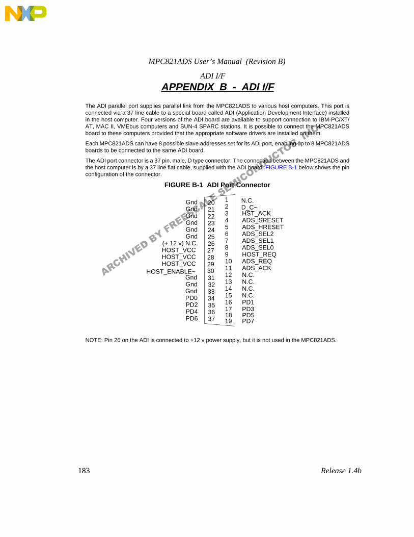
MPC821ADS User’s Manual (Revision B)
183 Release 1.4b
ADI I/F
APPENDIX B - ADI I/F
The ADI parallel port supplies parallel link from the MPC821ADS to various host computers. This port isconnected via a 37 line cable to a special board called ADI (Application Development Interface) installedin the host computer. Four versions of the ADI board are available to support connection to IBM-PC/XT/AT, MAC II, VMEbus computers and SUN-4 SPARC stations. It is possible to connect the MPC821ADSboard to these computers provided that the appropriate software drivers are installed on them.
Each MPC821ADS can have 8 possible slave addresses set for its ADI port, enabling up to 8 MPC821ADSboards to be connected to the same ADI board.
The ADI port connector is a 37 pin, male, D type connector. The connection between the MPC821ADS andthe host computer is by a 37 line flat cable, supplied with the ADI board. FIGURE B-1 below shows the pinconfiguration of the connector.
FIGURE B-1 ADI Port Connector
NOTE: Pin 26 on the ADI is connected to +12 v power supply, but it is not used in the MPC821ADS.
Gnd 20 N.C.12Gnd 21
Gnd 22Gnd 23Gnd 24Gnd 25
(+ 12 v) N.C. 26
HST_ACK3ADS_SRESET4
HOST_VCC
ADS_HRESETADS_SEL2ADS_SEL1ADS_SEL0
567827
HOST_VCCHOST_VCC
GndGnd
HOST_ENABLE~
HOST_REQADS_REQADS_ACKN.C.N.C.N.C.
91011121314
2829303132
Gnd 33PD0 34PD2PD4PD6
N.C.PD1PD3PD5PD7
1516171819
353637
D_C~
ARCHIVED BY FREESCALE SEMICONDUCTOR, INC.

MPC821ADS User’s Manual (Revision B)
184 Release 1.4b
ADI I/FB•1 ADI Port Signal Description The ADI port on the MPC821ADS was slightly modified to generate either hard reset or soft reset. Thisfeature was added to comply with the MPC821’s reset mechanism.
In the list below, the directions ’I’, ’O’, and ’I/O’ are relative to the MPC821ADS board. (I.E. ’I’ means inputto the MPC821ADS)
NOTE:Since the ADI was originated for the DSP56001ADS some of its signals throughout the boards it was used with, were designated with the prefix "ADS". This con-vention is kept with this design also.
• ADS_SEL(0:2) - ’I’
These three input lines determine the slave address of the MPC821ADS being accessed by the host computer. Up to 8 boards can be addressed by one ADI board.
• ADS_SRESET - ’I’
This input line is used to generate Soft Reset for the MPC821. When an ads is selected and this line is asserted by the host computer, Soft Reset will be generated to the MPC821 along with the Soft Reset configuration applied during that sequence.
• HOST_ENABLE~ - ’I’
This line is always driven low by the ADI board. When an ADI is connected to the MPC821ADS, this signals enabled the operation of the debug port controller. Otherwise the debug port control-ler is disabled and its outputs are tri-stated.
• ADS_HRESET - ’I’
When a host is connected, this line is used in conjunction with the addressing lines to generate a Hard Reset to the MPC821ADS board. When this signal is driven in conjunction with the ADS_SRESET signal, the ADI I/F state machines and registers are reset.
• HOST_REQ -’I’
This signal initiates a host to MPC821ADS write cycle.
• ADS_ACK - ’O’
This signal is the MPC821ADS response to the HOST_REQ signal, indicating that the board has detected the assertion of HOST_REQ.
• ADS_REQ - ’O’
This signal initiates an MPC821ADS to host write cycle.
• HST_ACK - ’I’
This signal serves as the host’s response to the ADS_REQ signal.
• HOST_VCC - ’I’ (three lines)
These lines are power lines from the host computer. In the MPC821ADS, these lines are used by the hardware to determine if the host computer is powered on.
• PD(0:7) - ’I/O’
These eight I/O lines are the parallel data bus. This bus is used to transmit and receive data from the hostcomputer.
ARCHIVED BY FREESCALE SEMICONDUCTOR, INC.

MPC821ADS User’s Manual (Revision B)
185 Release 1.4b
ADI Installation
APPENDIX C - ADI Installation
C•1 INTRODUCTIONThis appendix describes the hardware installation of the ADI board into various host computers.
The installation instructions cover the following host computers:
1) IBM-PC/XT/AT
2) SUN - 4 (SBus interface)
C•2 IBM-PC/XT/AT to MPC821ADS InterfaceThe ADI board should be installed in one of the IBM-PC/XT/AT motherboard system expansion slots. Asingle ADI can control up to eight MPC821ADS boards. The ADI address in the computer is configured tobe at I/O memory addresses 100-102 (hex), but it may be reconfigured for an alternate address space.
CAUTIONBEFORE REMOVING OR INSTALLING ANY EQUIPMENT IN THE IBM-PC/XT/AT COMPUTER, TURN THE POWER OFF AND REMOVE THE POWER CORD.
C•2•1 ADI Installation in IBM-PC/XT/AT
Refer to the appropriate Installation and Setup manual of the IBM-PC/XT/AT computer for instructions onremoving the computer cover.
There are currently two revisions of the ADI card being shipped and/or at customer’s and vendor’s sites.The first is described below as the original style. The more recent version is marked 2.0 (referred to as2.0) and is slightly longer than the original, but still is not a full size ISA card. It does have the ISA 16 bitconnector, but only additional IRQ options are pinned out.
ADI Style OriginalThe ADI board address block should be configured at a free I/O address space in the computer. Theaddress must be unique and it must not fall within the address range of another card installed in thecomputer.
This ADI board address block can be configured to start at one of the three following addresses:
• $100 - This address is unassigned in the IBM-PC
• $200 - This address is usually used for the game port
• $300 - This address is defined as a prototype port
ARCHIVED BY FREESCALE SEMICONDUCTOR, INC.
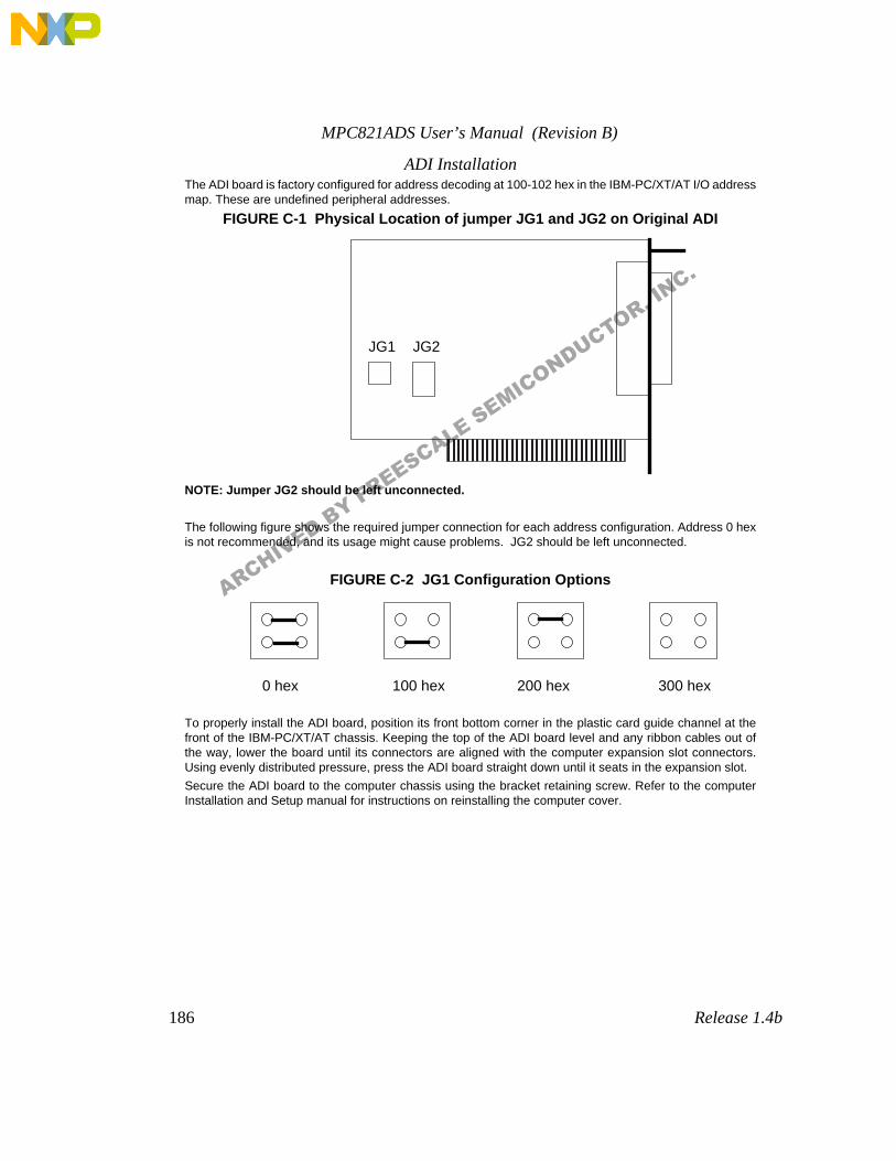
MPC821ADS User’s Manual (Revision B)
186 Release 1.4b
ADI InstallationThe ADI board is factory configured for address decoding at 100-102 hex in the IBM-PC/XT/AT I/O addressmap. These are undefined peripheral addresses.
FIGURE C-1 Physical Location of jumper JG1 and JG2 on Original ADI
NOTE: Jumper JG2 should be left unconnected.
The following figure shows the required jumper connection for each address configuration. Address 0 hexis not recommended, and its usage might cause problems. JG2 should be left unconnected.
FIGURE C-2 JG1 Configuration Options
To properly install the ADI board, position its front bottom corner in the plastic card guide channel at thefront of the IBM-PC/XT/AT chassis. Keeping the top of the ADI board level and any ribbon cables out ofthe way, lower the board until its connectors are aligned with the computer expansion slot connectors.Using evenly distributed pressure, press the ADI board straight down until it seats in the expansion slot.
Secure the ADI board to the computer chassis using the bracket retaining screw. Refer to the computerInstallation and Setup manual for instructions on reinstalling the computer cover.
JG1 JG2
0 hex 100 hex 200 hex 300 hex
ARCHIVED BY FREESCALE SEMICONDUCTOR, INC.
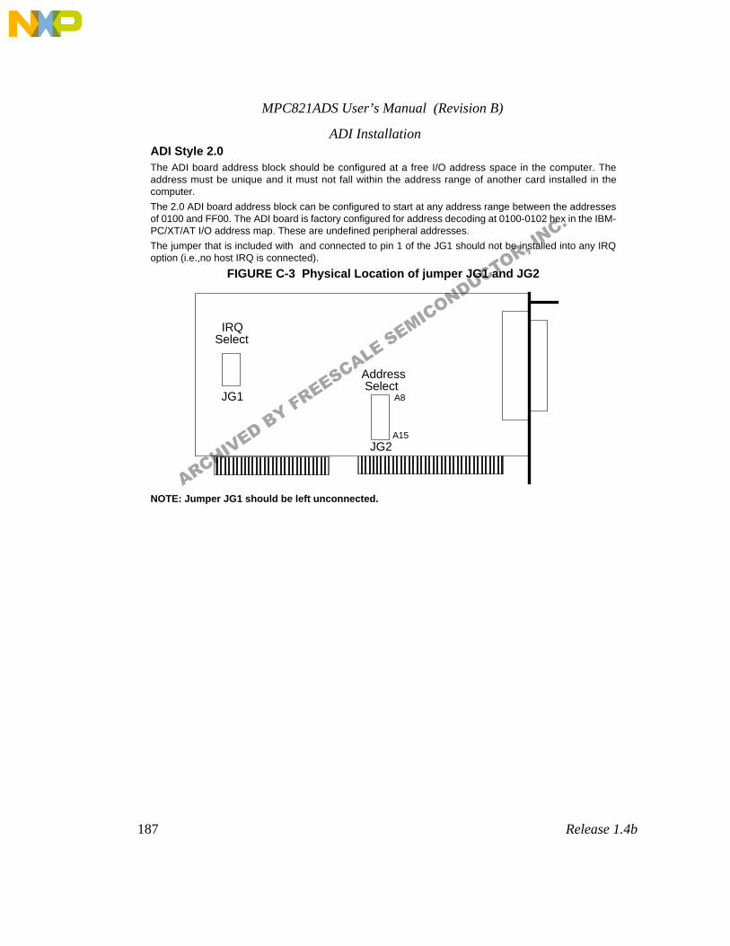
MPC821ADS User’s Manual (Revision B)
187 Release 1.4b
ADI InstallationADI Style 2.0The ADI board address block should be configured at a free I/O address space in the computer. Theaddress must be unique and it must not fall within the address range of another card installed in thecomputer.
The 2.0 ADI board address block can be configured to start at any address range between the addressesof 0100 and FF00. The ADI board is factory configured for address decoding at 0100-0102 hex in the IBM-PC/XT/AT I/O address map. These are undefined peripheral addresses.
The jumper that is included with and connected to pin 1 of the JG1 should not be installed into any IRQoption (i.e.,no host IRQ is connected).
FIGURE C-3 Physical Location of jumper JG1 and JG2
NOTE: Jumper JG1 should be left unconnected.
IRQ
AddressSelect
Select
A8
A15
JG1
JG2
ARCHIVED BY FREESCALE SEMICONDUCTOR, INC.
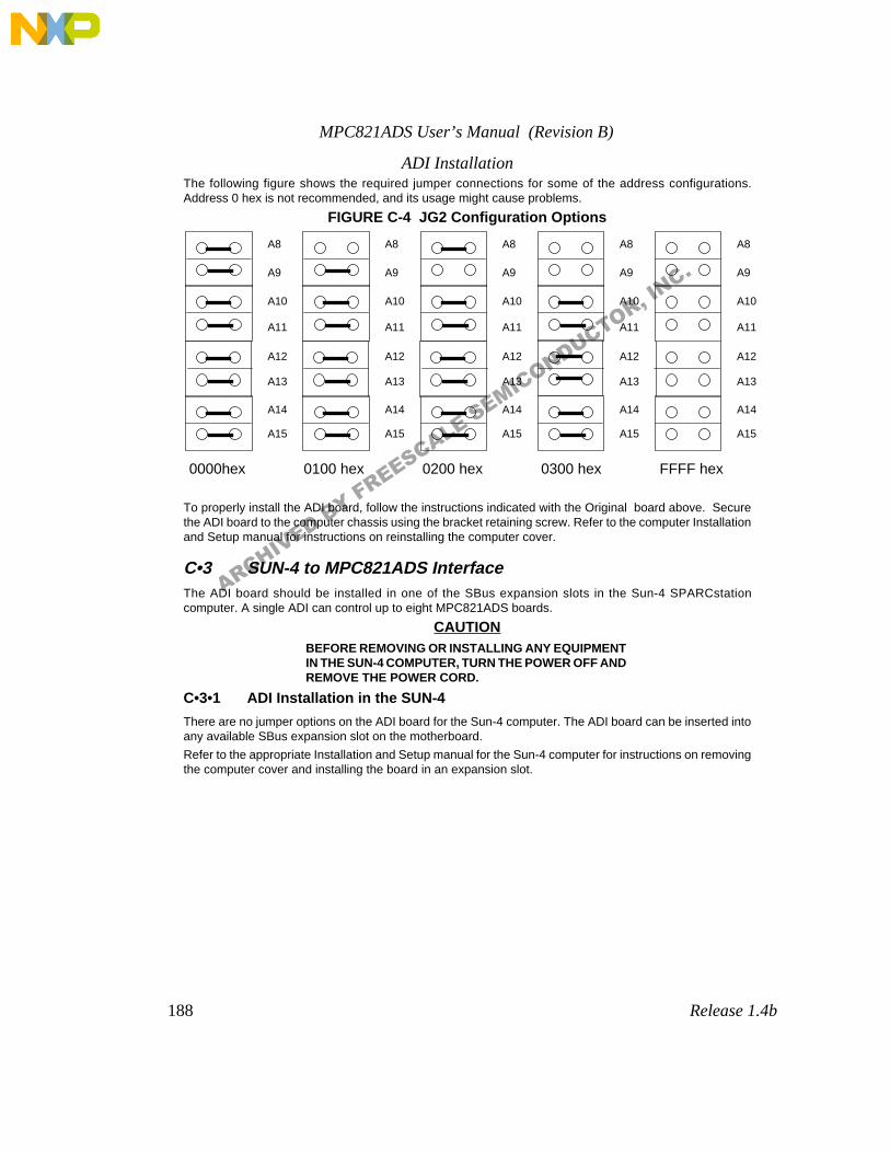
MPC821ADS User’s Manual (Revision B)
188 Release 1.4b
ADI InstallationThe following figure shows the required jumper connections for some of the address configurations.Address 0 hex is not recommended, and its usage might cause problems.
FIGURE C-4 JG2 Configuration Options
To properly install the ADI board, follow the instructions indicated with the Original board above. Securethe ADI board to the computer chassis using the bracket retaining screw. Refer to the computer Installationand Setup manual for instructions on reinstalling the computer cover.
C•3 SUN-4 to MPC821ADS InterfaceThe ADI board should be installed in one of the SBus expansion slots in the Sun-4 SPARCstationcomputer. A single ADI can control up to eight MPC821ADS boards.
CAUTIONBEFORE REMOVING OR INSTALLING ANY EQUIPMENT IN THE SUN-4 COMPUTER, TURN THE POWER OFF AND REMOVE THE POWER CORD.
C•3•1 ADI Installation in the SUN-4
There are no jumper options on the ADI board for the Sun-4 computer. The ADI board can be inserted intoany available SBus expansion slot on the motherboard.
Refer to the appropriate Installation and Setup manual for the Sun-4 computer for instructions on removingthe computer cover and installing the board in an expansion slot.
0000hex 0100 hex 0200 hex 0300 hex
A8
A15
A9
A10
A11
A12
A13
A14
FFFF hex
A8
A15
A9
A10
A11
A12
A13
A14
A8
A15
A9
A10
A11
A12
A13
A14
A8
A15
A9
A10
A11
A12
A13
A14
A8
A15
A9
A10
A11
A12
A13
A14
ARCHIVED BY FREESCALE SEMICONDUCTOR, INC.
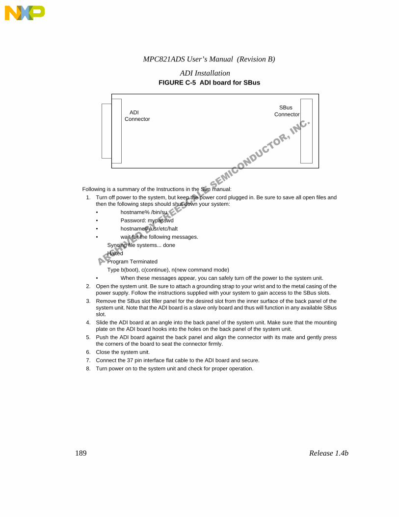
MPC821ADS User’s Manual (Revision B)
189 Release 1.4b
ADI InstallationFIGURE C-5 ADI board for SBus
Following is a summary of the Instructions in the Sun manual:
1. Turn off power to the system, but keep the power cord plugged in. Be sure to save all open files andthen the following steps should shut down your system:
• hostname% /bin/su
• Password: mypasswd
• hostname# /usr/etc/halt
• wait for the following messages.
Syncing file systems... done
Halted
Program Terminated
Type b(boot), c(continue), n(new command mode)
• When these messages appear, you can safely turn off the power to the system unit.
2. Open the system unit. Be sure to attach a grounding strap to your wrist and to the metal casing of thepower supply. Follow the instructions supplied with your system to gain access to the SBus slots.
3. Remove the SBus slot filler panel for the desired slot from the inner surface of the back panel of thesystem unit. Note that the ADI board is a slave only board and thus will function in any available SBusslot.
4. Slide the ADI board at an angle into the back panel of the system unit. Make sure that the mountingplate on the ADI board hooks into the holes on the back panel of the system unit.
5. Push the ADI board against the back panel and align the connector with its mate and gently pressthe corners of the board to seat the connector firmly.
6. Close the system unit.
7. Connect the 37 pin interface flat cable to the ADI board and secure.
8. Turn power on to the system unit and check for proper operation.
ADISBus
ConnectorConnector
ARCHIVED BY FREESCALE SEMICONDUCTOR, INC.

MPC821ADS User’s Manual (Revision B)
190 Release 1.4b
ADI Installation
ARCHIVED BY FREESCALE SEMICONDUCTOR, INC.

MPC821ADS User’s Manual (Revision B)
191 Release 1.4b
ADI Installation
ARCHIVED BY FREESCALE SEMICONDUCTOR, INC.