C H A P T E R 13 Output Stages and Power Amplifiers Power Amplifiers Power ≈ 1W Small signal model...
46
C H A P T E R 13 Output Stages and Power Amplifiers Power Amplifiers Power ≈ 1W Small signal model 不不不
-
Upload
malcolm-cain -
Category
Documents
-
view
221 -
download
3
Transcript of C H A P T E R 13 Output Stages and Power Amplifiers Power Amplifiers Power ≈ 1W Small signal model...
C H A P T E R 13
Output Stages and Power Amplifiers
Power Amplifiers Power ≈ 1WSmall signal model 不適用
2
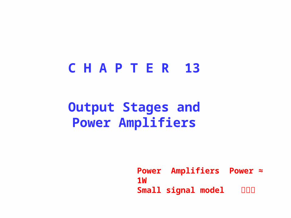
A. I IC I > IC , θ=360 B. IC = 0 , θ=180
Figure 13.1 Collector current waveforms for transistors operating in (a) class A, (b) class B, (c) class AB, and (d) class C amplifier stages.
3
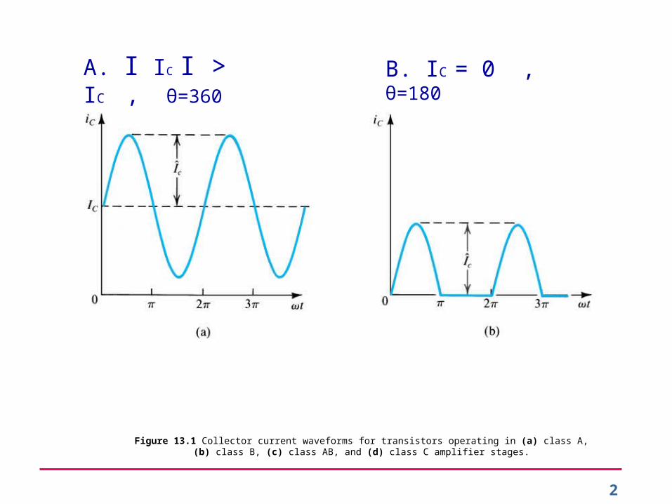
A B 類 . θ > 180 C. θ < 180 , 通訊
Figure 13.1 Collector current waveforms for transistors operating in (a) class A, (b) class B, (c) class AB, and (d) class C amplifier stages.
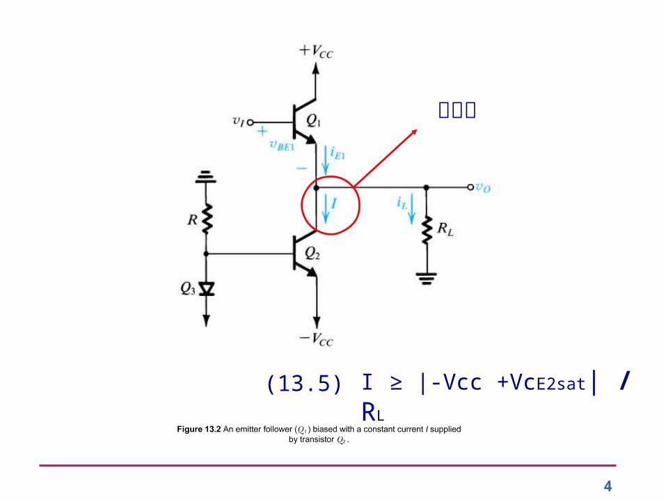
4
定電流
I ≥ |-Vcc +VcE2sat| / RL(13.5)
5
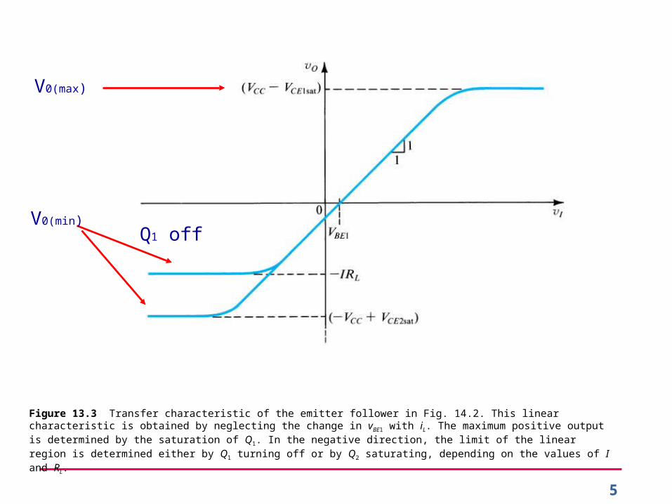
Figure 13.3 Transfer characteristic of the emitter follower in Fig. 14.2. This linear characteristic is obtained by neglecting the change in vBE1 with iL. The maximum positive output is determined by the saturation of Q1. In the negative direction, the limit of the linear region is determined either by Q1 turning off or by Q2 saturating, depending on the values of I and RL.
V0(max)
V0(min) Q1 off
6
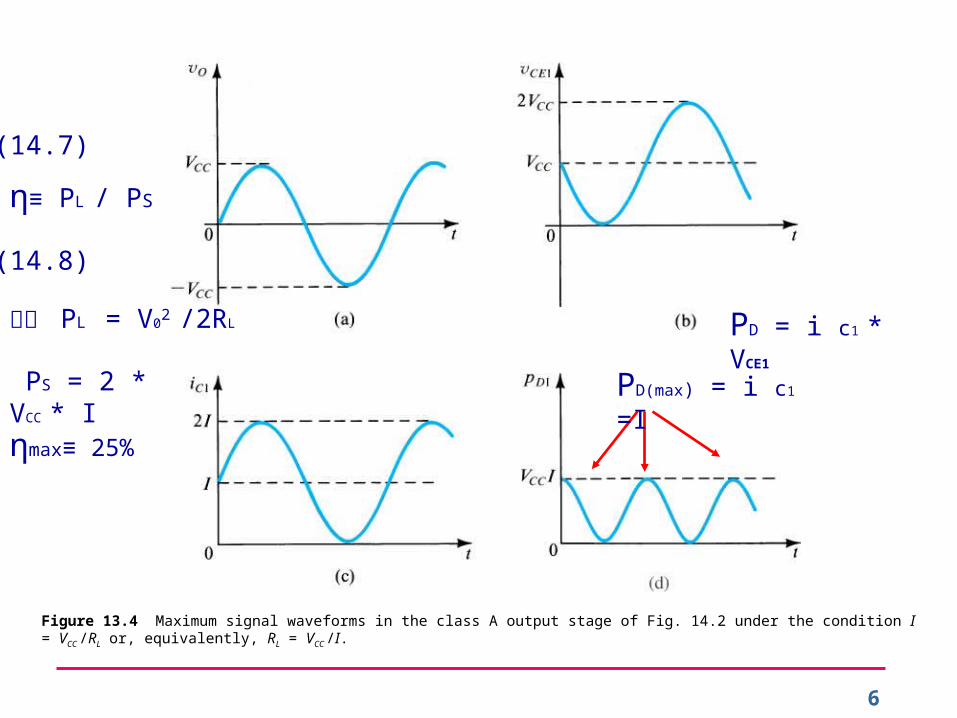
Figure 13.4 Maximum signal waveforms in the class A output stage of Fig. 14.2 under the condition I = VCC /RL or, equivalently, RL = VCC /I.
PD(max) = i c1 =I
PD = i c1 * VCE1
(14.7)
η≡ PL / PS
(14.8)
平均 PL = V02 /2RL
PS = 2 * VCC * I
ηmax≡ 25%
7
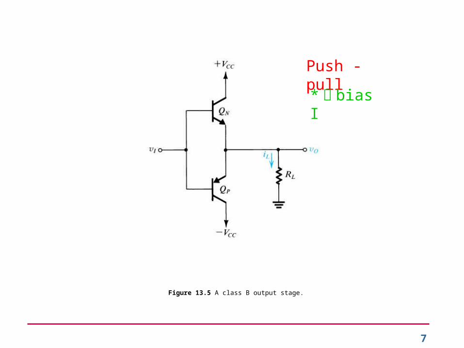
Push - pull
* 無 bias I
Figure 13.5 A class B output stage.
8
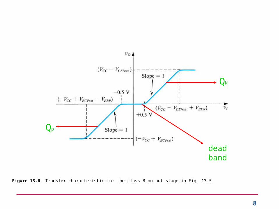
Figure 13.6 Transfer characteristic for the class B output stage in Fig. 13.5.
QN
Qp
dead band
9
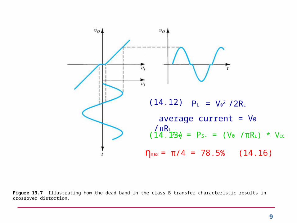
Figure 13.7 Illustrating how the dead band in the class B transfer characteristic results in crossover distortion.
(14.12) PL = V02 /2RL
average current = V0 /πRL
(14.13) PS+ = PS- = (V0 /πRL) * VCC
ηmax = π/4 = 78.5% (14.16)
10
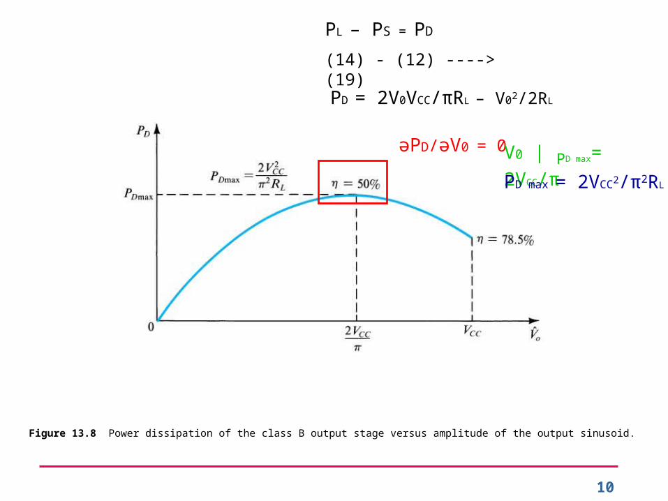
Figure 13.8 Power dissipation of the class B output stage versus amplitude of the output sinusoid.
PL – PS = PD
(14) - (12) ----> (19)
PD = 2V0VCC/πRL – V02/2RL
әPD/әV0 = 0 V0 | PD max= 2VCC/π
PD max = 2VCC2/π2RL
11
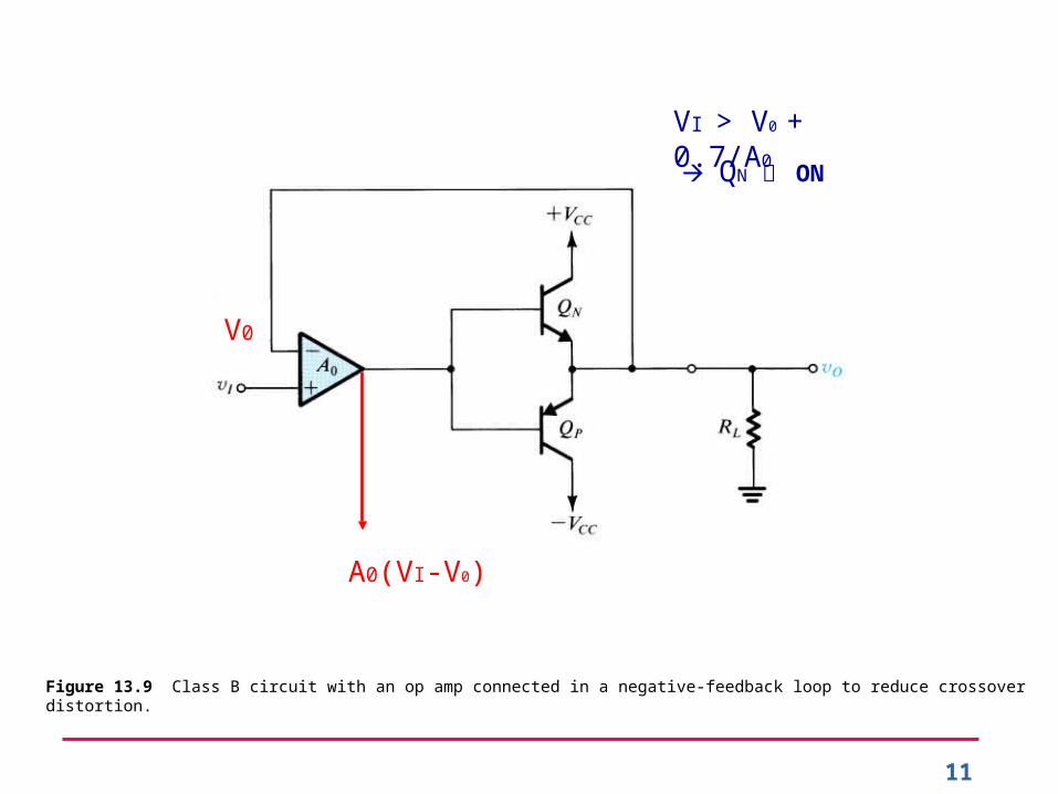
Figure 13.9 Class B circuit with an op amp connected in a negative-feedback loop to reduce crossover distortion.
A0(VI-V0)
V0
VI > V0 + 0.7/A0
QN 即 ON
Microelectronic Circuits, International Sixth Edition
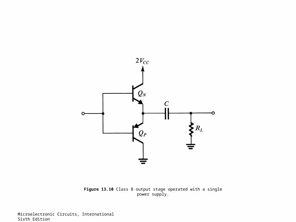
Figure 13.10 Class B output stage operated with a single power supply.
13
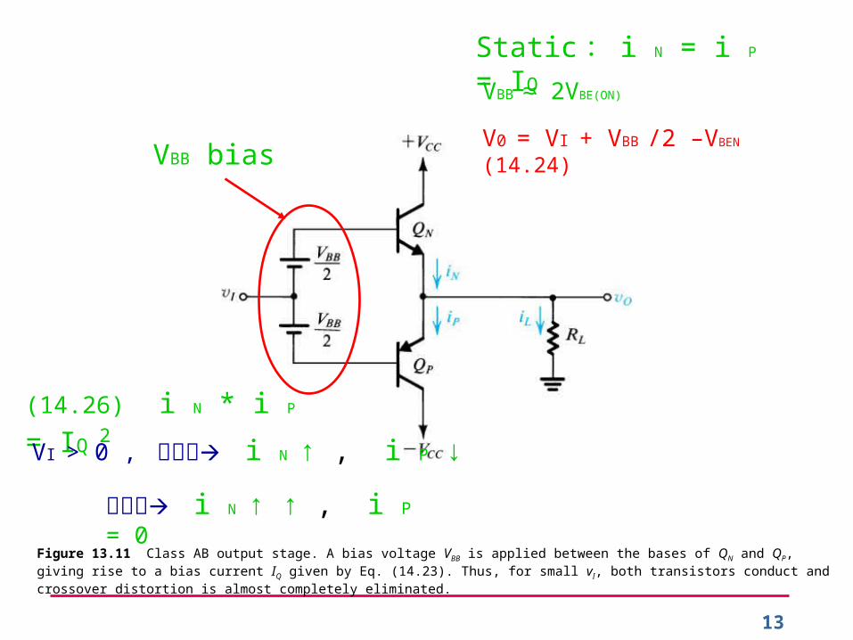
Figure 13.11 Class AB output stage. A bias voltage VBB is applied between the bases of QN and QP, giving rise to a bias current IQ given by Eq. (14.23). Thus, for small vI, both transistors conduct and crossover distortion is almost completely eliminated.
VBB bias
Static : i N = i P = IQ
VBB ≈ 2VBE(ON)
V0 = VI + VBB /2 –VBEN (14.24)
(14.26) i N * i P = IQ 2
VI > 0 , 且很小 i N ↑ , i P ↓
且很大 i N ↑ ↑ , i P = 0
Microelectronic Circuits, International Sixth Edition
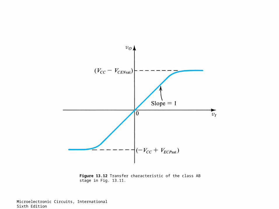
Figure 13.12 Transfer characteristic of the class AB stage in Fig. 13.11.
15
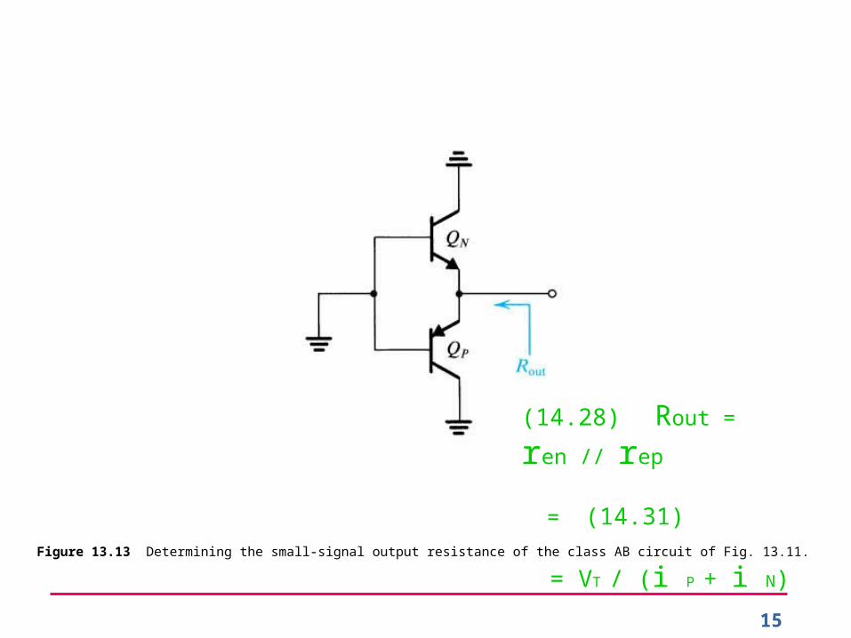
Figure 13.13 Determining the small-signal output resistance of the class AB circuit of Fig. 13.11.
(14.28) Rout = ren // rep
= (14.31) = VT / (i P + i N)
16
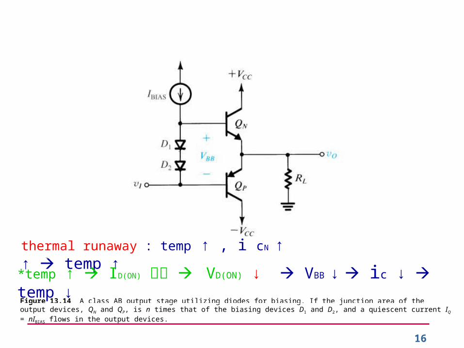
Figure 13.14 A class AB output stage utilizing diodes for biasing. If the junction area of the output devices, QN and QP, is n times that of the biasing devices D1 and D2, and a quiescent current IQ = nIBIAS flows in the output devices.
thermal runaway : temp ↑ , i cN ↑ ↑ temp ↑
*temp ↑ ID(ON) 不變 VD(ON) ↓ VBB ↓ ic ↓ temp ↓
17
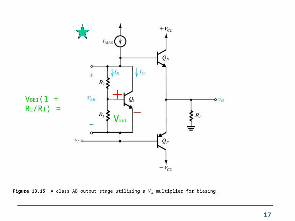
Figure 13.15 A class AB output stage utilizing a VBE multiplier for biasing.
VBE1(1 + R2/R1) =
VBE1
18
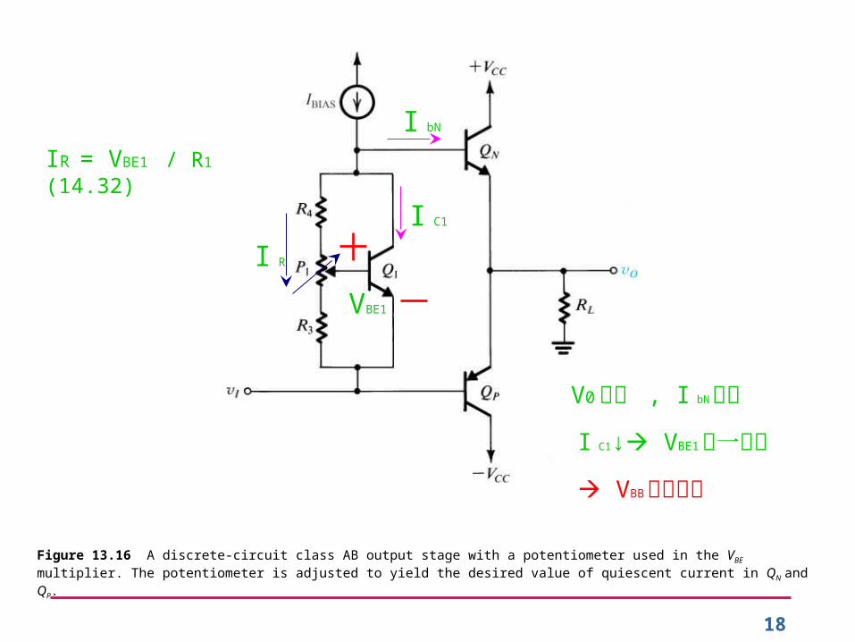
Figure 13.16 A discrete-circuit class AB output stage with a potentiometer used in the VBE multiplier. The potentiometer is adjusted to yield the desired value of quiescent current in QN and QP.
IR = VBE1 / R1 (14.32)
VBE1
I R
I C1
I bN
V0 很大 , I bN不小
I C1↓ VBE1小一點點
VBB幾乎不變
Microelectronic Circuits, International Sixth Edition
Microelectronic Circuits, International Sixth Edition
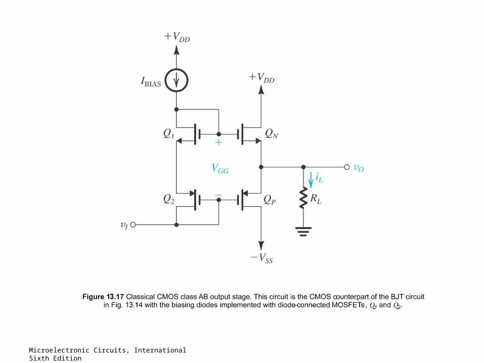
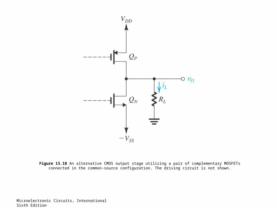
Figure 13.18 An alternative CMOS output stage utilizing a pair of complementary MOSFETs connected in the common-source configuration. The driving circuit is not shown.
Microelectronic Circuits, International Sixth Edition
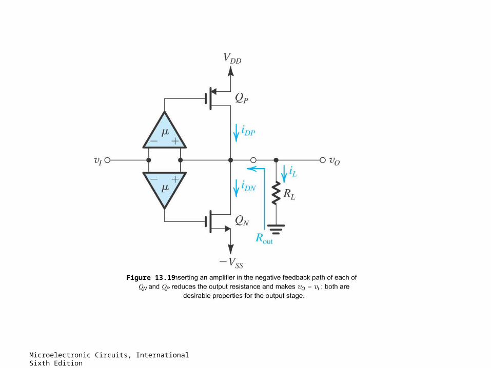
Figure 13.19
Microelectronic Circuits, International Sixth Edition
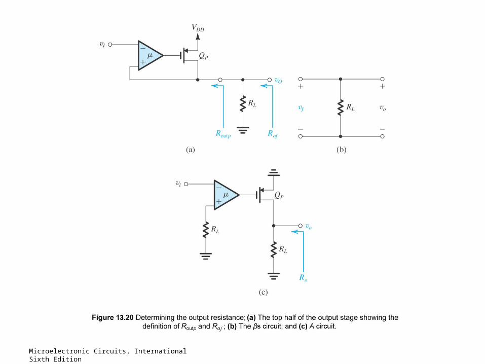
Microelectronic Circuits, International Sixth Edition
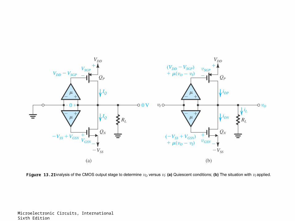
Figure 13.21
Microelectronic Circuits, International Sixth Edition
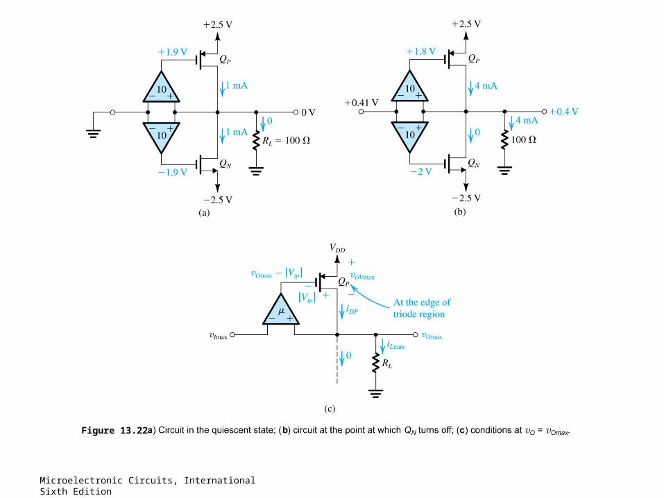
Figure 13.22
Microelectronic Circuits, International Sixth Edition
26
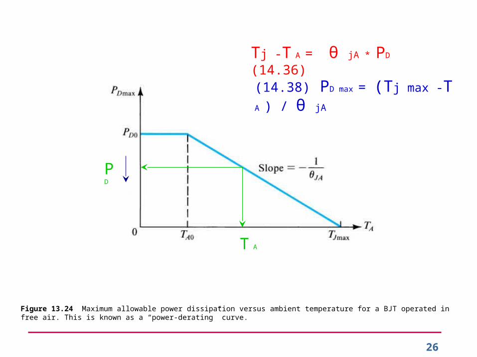
Figure 13.24 Maximum allowable power dissipation versus ambient temperature for a BJT operated in free air. This is known as a “power-derating” curve.
P D
T A
Tj -T A = θ jA * PD (14.36)
(14.38) PD max = (Tj max -T A ) / θ jA
Microelectronic Circuits, International Sixth Edition
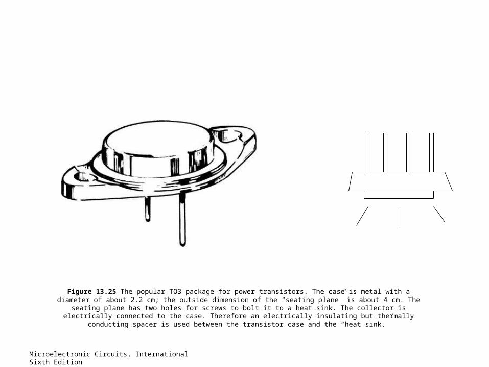
Figure 13.25 The popular TO3 package for power transistors. The case is metal with a diameter of about 2.2 cm; the outside dimension of the “seating plane” is about 4 cm. The seating plane has two holes for screws to bolt it to a heat sink. The
collector is electrically connected to the case. Therefore an electrically insulating but thermally conducting spacer is used between the transistor case and the “heat sink.”
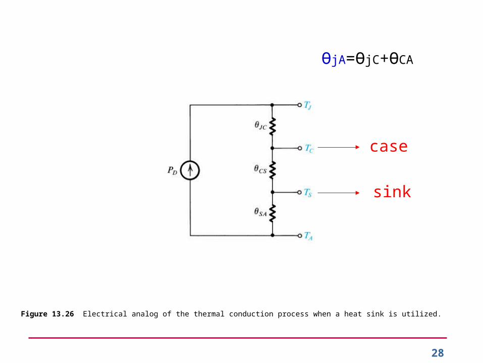
28
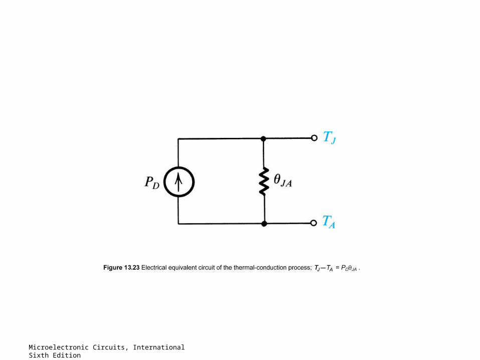
Figure 13.26 Electrical analog of the thermal conduction process when a heat sink is utilized.
case
sink
ӨjA=ӨjC+ӨCA
29
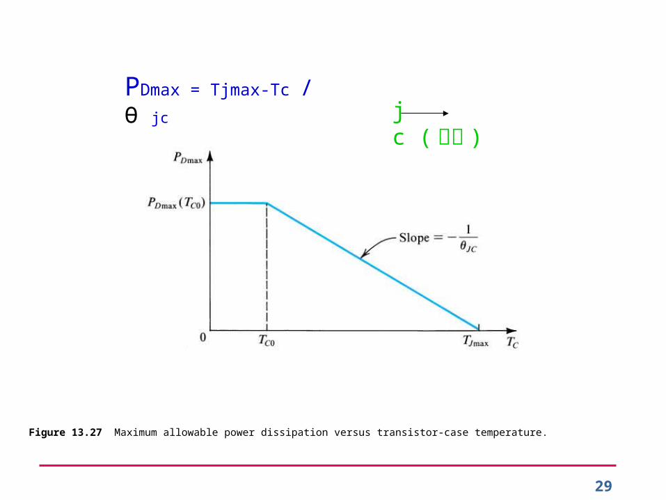
Figure 13.27 Maximum allowable power dissipation versus transistor-case temperature.
PDmax = Tjmax-Tc / Ө jc j c ( 廠
商 )
30
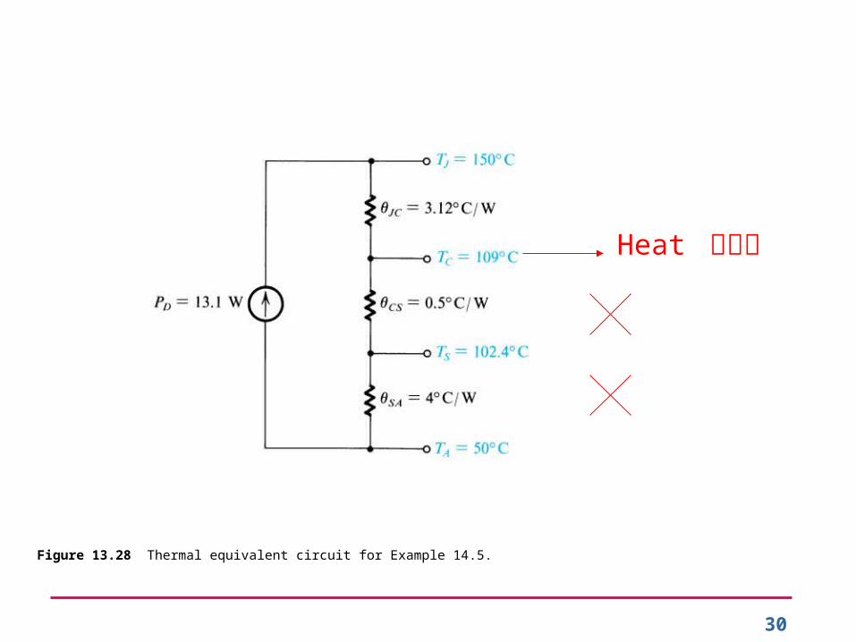
Figure 13.28 Thermal equivalent circuit for Example 14.5.
Heat 全沒了
31
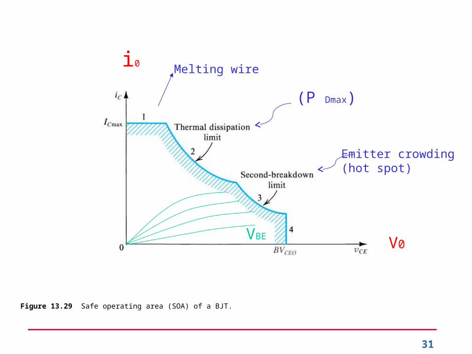
Figure 13.29 Safe operating area (SOA) of a BJT.
i0
V0
Melting wire
(P Dmax)
Emitter crowding(hot spot)
VBE
32
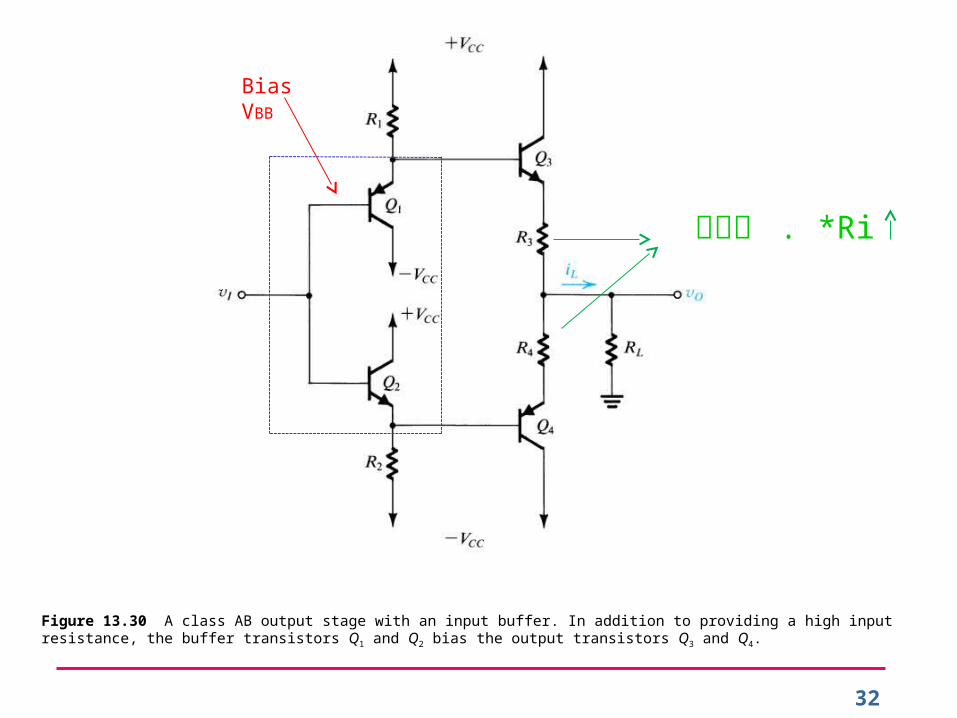
Figure 13.30 A class AB output stage with an input buffer. In addition to providing a high input resistance, the buffer transistors Q1 and Q2 bias the output transistors Q3 and Q4.
Bias VBB
負回授 . *Ri
33
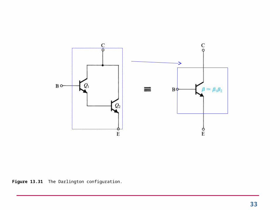
Figure 13.31 The Darlington configuration.
Microelectronic Circuits, International Sixth Edition
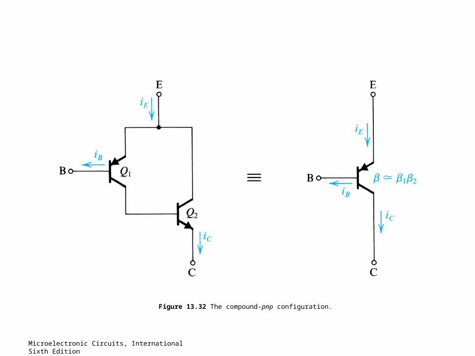
Figure 13.32 The compound-pnp configuration.
35
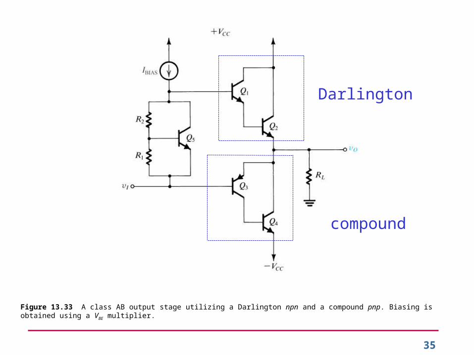
Figure 13.33 A class AB output stage utilizing a Darlington npn and a compound pnp. Biasing is obtained using a VBE multiplier.
Darlington
compound
36
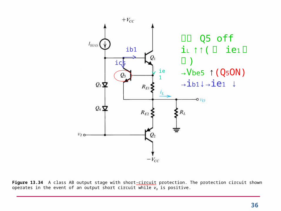
Figure 13.34 A class AB output stage with short-circuit protection. The protection circuit shown operates in the event of an output short circuit while vO is positive.
平時 Q5 offiL ↑↑( 及 ie1 很大 )→Vbe5 ↑(Q5ON)→ib1↓→ie1 ↓
ib1
icsie1
37
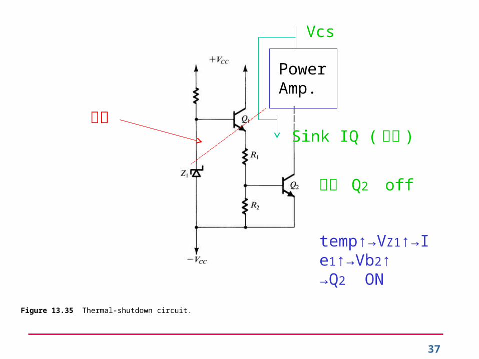
Figure 13.35 Thermal-shutdown circuit.
PowerAmp.
Vcs
Sink IQ ( 並聯 )導熱
平時 Q2 off
temp↑→VZ1↑→Ie1↑→Vb2↑→Q2 ON
38
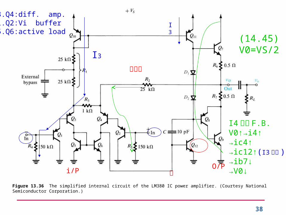
Figure 13.36 The simplified internal circuit of the LM380 IC power amplifier. (Courtesy National Semiconductor Corporation.)
(14.45)V0=VS/2
Q3.Q4:diff. amp.Q1.Q2:Vi bufferQ5.Q6:active load
I3
負回授
I4 為負 F.B.V0↑→i4↑→ic4↑→ic12↑(I3 固定 )→ib7↓→V0↓主
O/Pi/P
I3
39
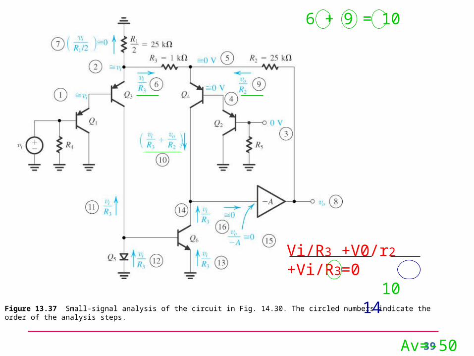
Figure 13.37 Small-signal analysis of the circuit in Fig. 14.30. The circled numbers indicate the order of the analysis steps.
6 + 9 = 10
Vi/R3 +V0/r2 +Vi/R3=0 10 14 Av=-50
Microelectronic Circuits, International Sixth Edition
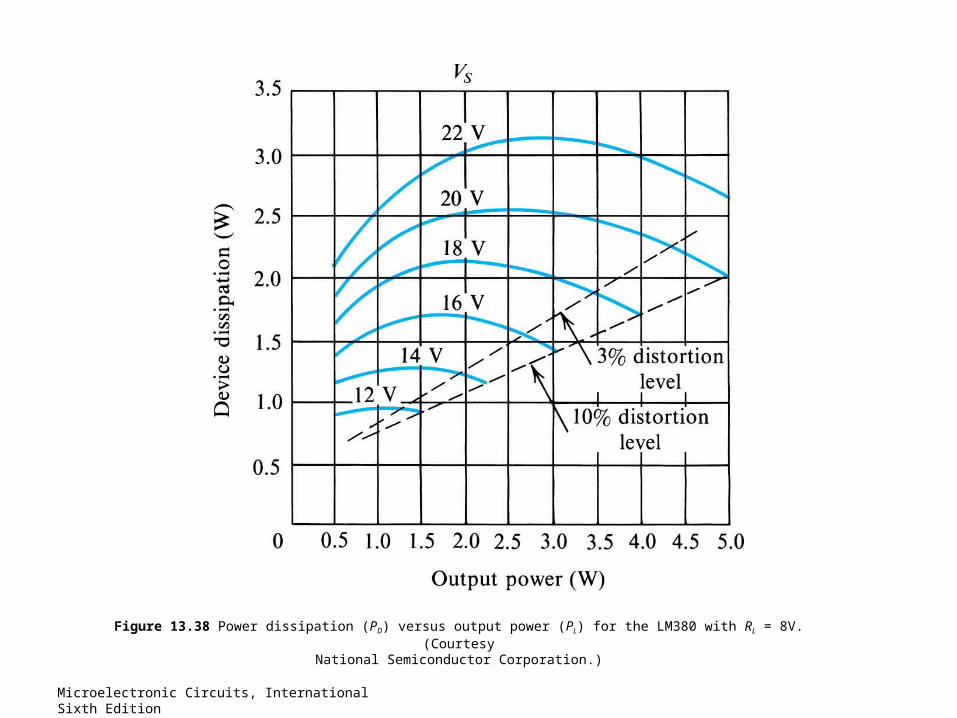
Figure 13.38 Power dissipation (PD) versus output power (PL) for the LM380 with RL = 8V. (CourtesyNational Semiconductor Corporation.)
41
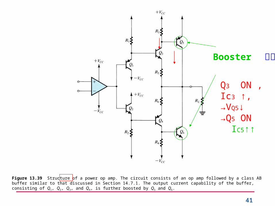
Figure 13.39 Structure of a power op amp. The circuit consists of an op amp followed by a class AB buffer similar to that discussed in Section 14.7.1. The output current capability of the buffer, consisting of Q1, Q2, Q3, and Q4, is further boosted by Q5 and Q6.
Booster 增幅
Q3 ON ,Ic3 ↑,→VQ5↓→Q5 ON IC5↑↑
42
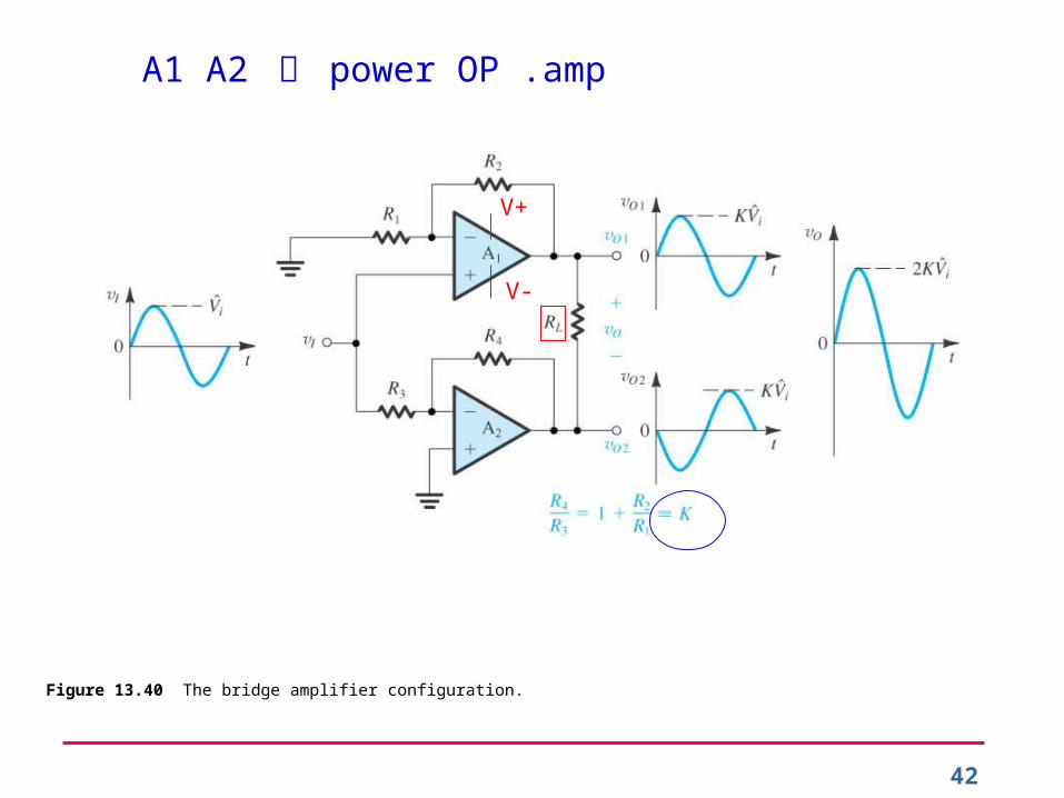
Figure 13.40 The bridge amplifier configuration.
V+
V-
A1 A2 為 power OP .amp
43
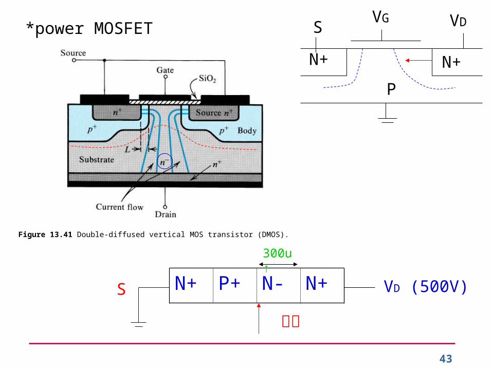
Figure 13.41 Double-diffused vertical MOS transistor (DMOS).
*power MOSFET
N+ P+ N- N+
壓降
300u↑
VD (500V)S
P
N+ N+
VGS VD
44
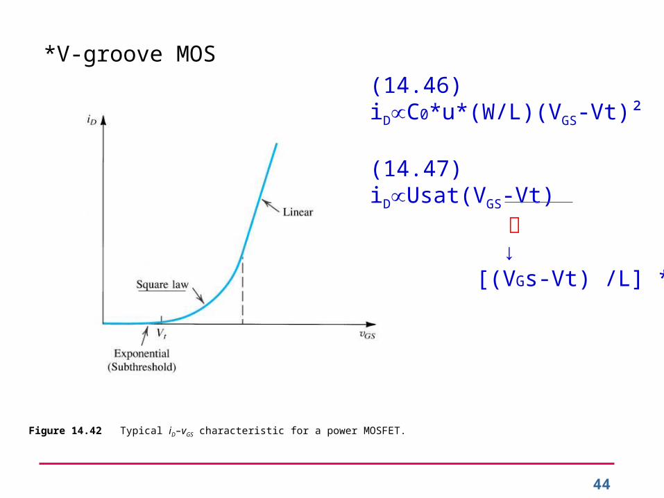
Figure 14.42 Typical iD–vGS characteristic for a power MOSFET.
*V-groove MOS
(14.46)iD C∝ 0*u*(W/L)(VGS-Vt)²
(14.47)iD Usat(V∝ GS-Vt) 定 ↓ [(VGs-Vt) /L] * u
45
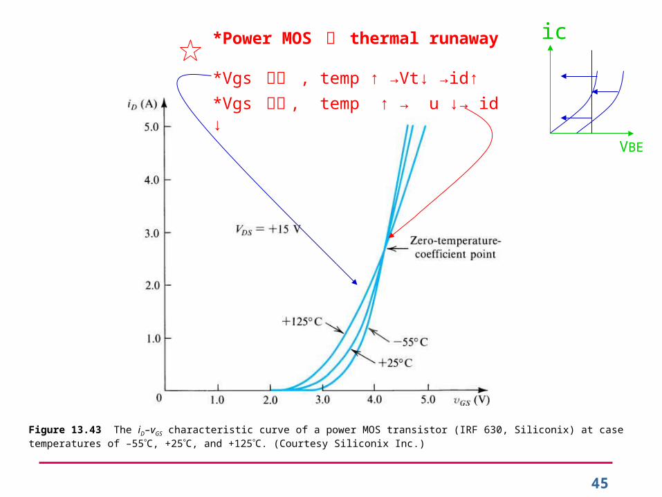
Figure 13.43 The iD–vGS characteristic curve of a power MOS transistor (IRF 630, Siliconix) at case temperatures of –55 C, +25C, and +125C. (Courtesy Siliconix Inc.)
*Power MOS 無 thermal runaway
*Vgs 小時 , temp ↑ →Vt↓ →id↑
*Vgs 大時 , temp ↑ → u ↓→ id ↓
ic
VBE
46
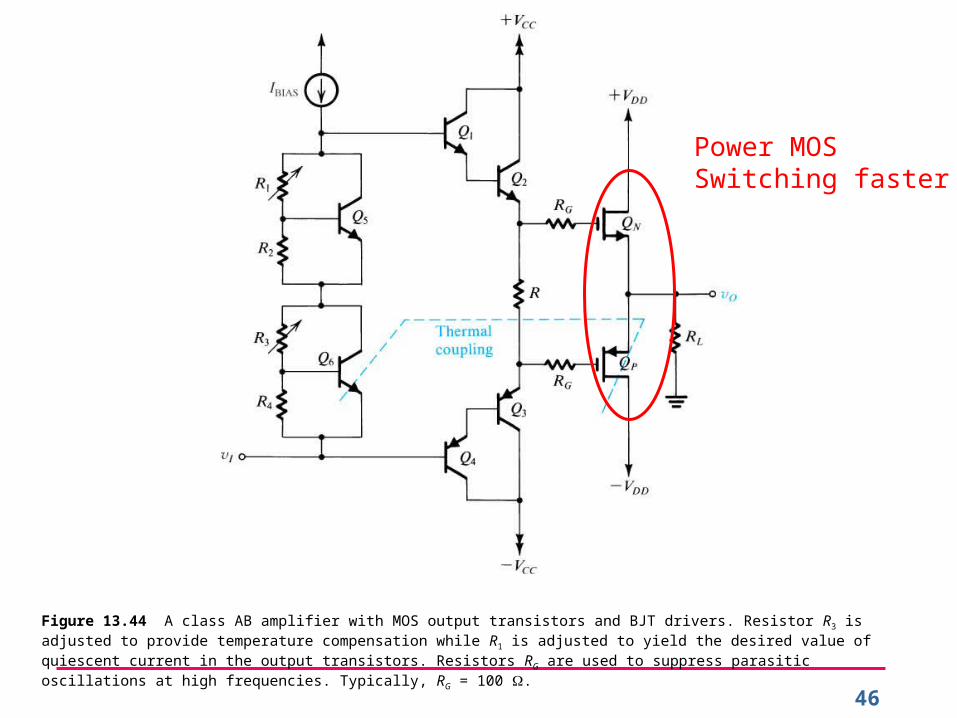
Figure 13.44 A class AB amplifier with MOS output transistors and BJT drivers. Resistor R3 is adjusted to provide temperature compensation while R1 is adjusted to yield the desired value of quiescent current in the output transistors. Resistors RG are used to suppress parasitic oscillations at high frequencies. Typically, RG = 100 .
Power MOSSwitching faster