bq2947 Overvoltage Protection for 2-Series to 4-Series ... · VDD 1 8 OUT V4 2 7 CD V3 3 6 VSS V2 4...
30
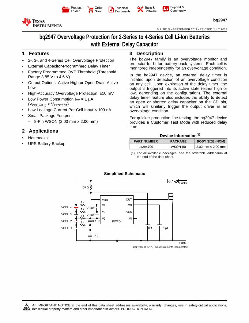
100 Ω VCELL1 VCELL3 VCELL2 OUT VDD VSS 0.1µF 1k 1k Pack+ Pack– V3 V2 V1 V4 CD VCELL4 PWPD 0.1µF 0.1µF 0.1µF 0.1µF 1k 1k 0.1µF Copyright © 2017, Texas Instruments Incorporated Product Folder Order Now Technical Documents Tools & Software Support & Community An IMPORTANT NOTICE at the end of this data sheet addresses availability, warranty, changes, use in safety-critical applications, intellectual property matters and other important disclaimers. PRODUCTION DATA. bq2947 SLUSB15I – SEPTEMBER 2012 – REVISED JULY 2018 bq2947 Overvoltage Protection for 2-Series to 4-Series Cell Li-Ion Batteries with External Delay Capacitor 1 1 Features 1• 2-, 3-, and 4-Series Cell Overvoltage Protection • External Capacitor-Programmed Delay Timer • Factory Programmed OVP Threshold (Threshold Range 3.85 V to 4.6 V) • Output Options: Active High or Open Drain Active Low • High-Accuracy Overvoltage Protection: ±10 mV • Low Power Consumption I CC ≈ 1 μA (V CELL(ALL) <V PROTECT ) • Low Leakage Current Per Cell Input < 100 nA • Small Package Footprint – 8-Pin WSON (2.00 mm x 2.00 mm) 2 Applications • Notebooks • UPS Battery Backup 3 Description The bq2947 family is an overvoltage monitor and protector for Li-Ion battery pack systems. Each cell is monitored independently for an overvoltage condition. In the bq2947 device, an external delay timer is initiated upon detection of an overvoltage condition on any cell. Upon expiration of the delay timer, the output is triggered into its active state (either high or low, depending on the configuration). The external delay timer feature also includes the ability to detect an open or shorted delay capacitor on the CD pin, which will similarly trigger the output driver in an overvoltage condition. For quicker production-line testing, the bq2947 device provides a Customer Test Mode with reduced delay time. Device Information (1) PART NUMBER PACKAGE BODY SIZE (NOM) bq294700 WSON (8) 2.00 mm × 2.00 mm (1) For all available packages, see the orderable addendum at the end of the data sheet. spacer Simplified Schematic
Transcript of bq2947 Overvoltage Protection for 2-Series to 4-Series ... · VDD 1 8 OUT V4 2 7 CD V3 3 6 VSS V2 4...
100 Ω
VCELL1
VCELL3
VCELL2
OUTVDD
VSS
0.1 µF
1k
1k
Pack+
Pack–
V3
V2 V1
V4 CDVCELL4
PWPD
0.1 µF
0.1µF
0.1µF
0.1µF
1k
1k
0.1µF
Copyright © 2017, Texas Instruments Incorporated
Product
Folder
Order
Now
Technical
Documents
Tools &
Software
Support &Community
An IMPORTANT NOTICE at the end of this data sheet addresses availability, warranty, changes, use in safety-critical applications,intellectual property matters and other important disclaimers. PRODUCTION DATA.
bq2947
SLUSB15I –SEPTEMBER 2012–REVISED JULY 2018
bq2947 Overvoltage Protection for 2-Series to 4-Series Cell Li-Ion Batterieswith External Delay Capacitor
1
1 Features1• 2-, 3-, and 4-Series Cell Overvoltage Protection• External Capacitor-Programmed Delay Timer• Factory Programmed OVP Threshold (Threshold
Range 3.85 V to 4.6 V)• Output Options: Active High or Open Drain Active
Low• High-Accuracy Overvoltage Protection: ±10 mV• Low Power Consumption ICC ≈ 1 µA
(VCELL(ALL) < VPROTECT)• Low Leakage Current Per Cell Input < 100 nA• Small Package Footprint
– 8-Pin WSON (2.00 mm x 2.00 mm)
2 Applications• Notebooks• UPS Battery Backup
3 DescriptionThe bq2947 family is an overvoltage monitor andprotector for Li-Ion battery pack systems. Each cell ismonitored independently for an overvoltage condition.
In the bq2947 device, an external delay timer isinitiated upon detection of an overvoltage conditionon any cell. Upon expiration of the delay timer, theoutput is triggered into its active state (either high orlow, depending on the configuration). The externaldelay timer feature also includes the ability to detectan open or shorted delay capacitor on the CD pin,which will similarly trigger the output driver in anovervoltage condition.
For quicker production-line testing, the bq2947 deviceprovides a Customer Test Mode with reduced delaytime.
Device Information(1)
PART NUMBER PACKAGE BODY SIZE (NOM)bq294700 WSON (8) 2.00 mm × 2.00 mm
(1) For all available packages, see the orderable addendum atthe end of the data sheet.
spacer
Simplified Schematic
2
bq2947
SLUSB15I –SEPTEMBER 2012–REVISED JULY 2018 www.ti.com
Product Folder Links: bq2947
Submit Documentation Feedback Copyright © 2012–2018, Texas Instruments Incorporated
Table of Contents1 Features .................................................................. 12 Applications ........................................................... 13 Description ............................................................. 14 Revision History..................................................... 25 Device Options....................................................... 36 Pin Configuration and Functions ......................... 47 Specifications......................................................... 4
7.1 Absolute Maximum Ratings ...................................... 47.2 ESD Ratings.............................................................. 47.3 Recommended Operating Conditions....................... 57.4 Thermal Information .................................................. 57.5 Electrical Characteristics........................................... 57.6 Typical Characteristics .............................................. 7
8 Detailed Description .............................................. 88.1 Overview ................................................................... 88.2 Functional Block Diagram ......................................... 88.3 Feature Description................................................... 8
8.4 Device Functional Modes........................................ 109 Application and Implementation ........................ 12
9.1 Application Information............................................ 129.2 Typical Applications ................................................ 12
10 Power Supply Recommendations ..................... 1511 Layout................................................................... 15
11.1 Layout Guidelines ................................................. 1511.2 Layout Example .................................................... 15
12 Device and Documentation Support ................. 1612.1 Documentation Support ........................................ 1612.2 Receiving Notification of Documentation Updates 1612.3 Community Resources.......................................... 1612.4 Trademarks ........................................................... 1612.5 Electrostatic Discharge Caution............................ 1612.6 Glossary ................................................................ 16
13 Mechanical, Packaging, and OrderableInformation ........................................................... 16
4 Revision HistoryNOTE: Page numbers for previous revisions may differ from page numbers in the current version.
Changes from Revision H (February 2018) to Revision I Page
• Added bq294713 to the Device Options table........................................................................................................................ 3• Added bq294713 to the Electrical Characteristics ................................................................................................................. 5
Changes from Revision G (November 2017) to Revision H Page
• Changed bq294712 to Production Data in the Device Options table .................................................................................... 3
Changes from Revision F (January 2017) to Revision G Page
• Deleted bq294709 from the Device Options table.................................................................................................................. 3• Added bq294712 to the Device Options table........................................................................................................................ 3• Added bq294712 and deleted bq294709 in Electrical Characteristics .................................................................................. 5
Changes from Revision E (February 2016) to Revision F Page
• Added bq294711 to the Device Options table........................................................................................................................ 3• Added Receiving Notification of Documentation Updates ................................................................................................... 16
Changes from Revision D (November 2015) to Revision E Page
• Changed bq297406 device status From: Product Preview To: Active in the Device Options table ...................................... 3
Changes from Revision C (November 2015) to Revision D Page
• Changed the device number to bq2947 ................................................................................................................................ 1• Deleted the Related Links table from the Device and Documentation Support section....................................................... 16
3
bq2947
www.ti.com SLUSB15I –SEPTEMBER 2012–REVISED JULY 2018
Product Folder Links: bq2947
Submit Documentation FeedbackCopyright © 2012–2018, Texas Instruments Incorporated
Changes from Revision B (August 2014) to Revision C Page
• Added preview footnote to the Device Options table ............................................................................................................ 3• Added bq294708 to the Device Options table........................................................................................................................ 3
Changes from Revision A (June 2013) to Revision B Page
• Added ESD Ratings table, Feature Description section, Device Functional Modes, Application and Implementationsection, Power Supply Recommendations section, Layout section, Device and Documentation Support section, andMechanical, Packaging, and Orderable Information section .................................................................................................. 1
Changes from Original (September 2012) to Revision A Page
• Added the bq294707 device to Production Data.................................................................................................................... 1
(1) Contact TI for more information.
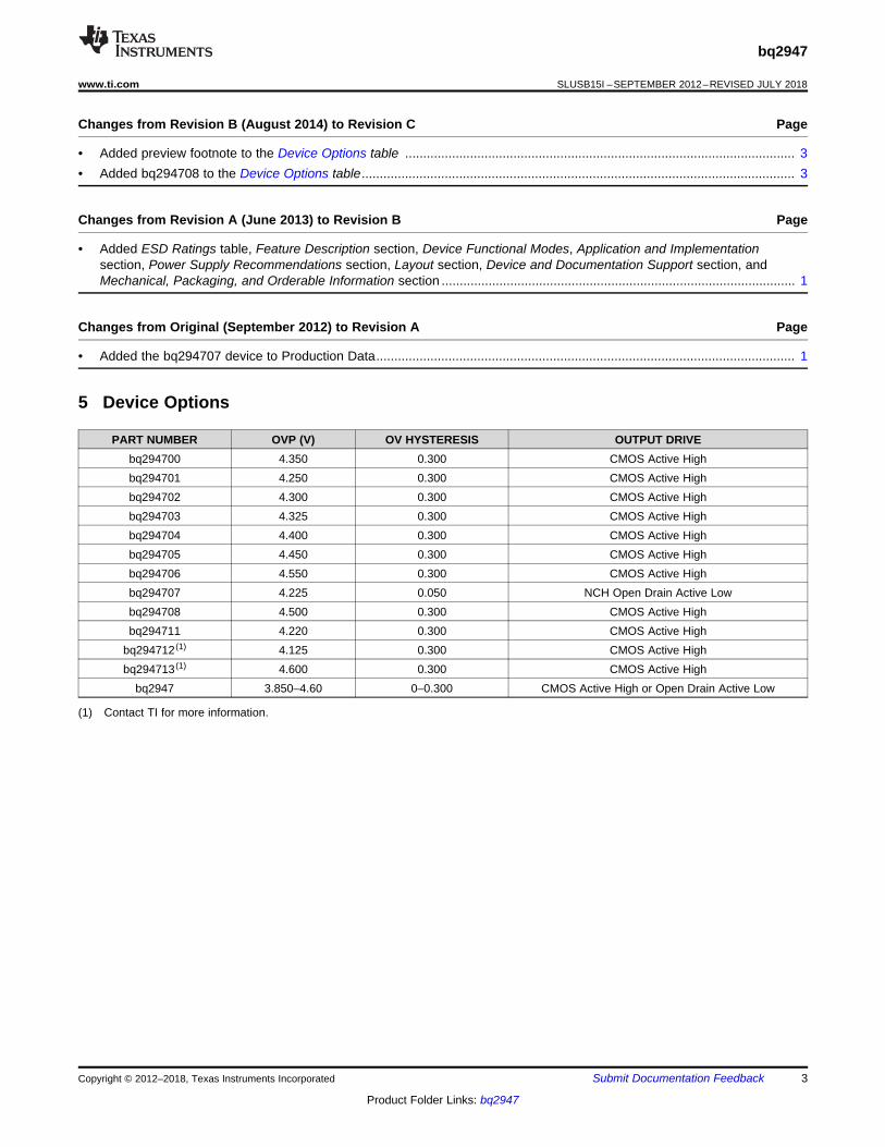
5 Device Options
PART NUMBER OVP (V) OV HYSTERESIS OUTPUT DRIVEbq294700 4.350 0.300 CMOS Active Highbq294701 4.250 0.300 CMOS Active Highbq294702 4.300 0.300 CMOS Active Highbq294703 4.325 0.300 CMOS Active Highbq294704 4.400 0.300 CMOS Active Highbq294705 4.450 0.300 CMOS Active Highbq294706 4.550 0.300 CMOS Active Highbq294707 4.225 0.050 NCH Open Drain Active Lowbq294708 4.500 0.300 CMOS Active Highbq294711 4.220 0.300 CMOS Active High
bq294712 (1) 4.125 0.300 CMOS Active Highbq294713 (1) 4.600 0.300 CMOS Active High
bq2947 3.850–4.60 0–0.300 CMOS Active High or Open Drain Active Low
1VDD 8 OUT
2V4 7 CD
3V3 6 VSS
4V2 5 V1
Not to scale
Thermal
Pad
4
bq2947
SLUSB15I –SEPTEMBER 2012–REVISED JULY 2018 www.ti.com
Product Folder Links: bq2947
Submit Documentation Feedback Copyright © 2012–2018, Texas Instruments Incorporated
(1) IA = Input Analog, OA = Output Analog, P = Power Connection
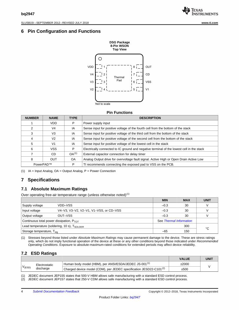
6 Pin Configuration and Functions
DSG Package8-Pin WSON
Top View
Pin FunctionsNUMBER NAME TYPE DESCRIPTION
1 VDD P Power supply input2 V4 IA Sense input for positive voltage of the fourth cell from the bottom of the stack3 V3 IA Sense input for positive voltage of the third cell from the bottom of the stack4 V2 IA Sense input for positive voltage of the second cell from the bottom of the stack5 V1 IA Sense input for positive voltage of the lowest cell in the stack6 VSS P Electrically connected to IC ground and negative terminal of the lowest cell in the stack7 CD OA (1) External capacitor connection for delay timer8 OUT OA Analog Output drive for overvoltage fault signal. Active High or Open Drain Active Low
PowerPAD™ P TI recommends connecting the exposed pad to VSS on the PCB.
(1) Stresses beyond those listed under Absolute Maximum Ratings may cause permanent damage to the device. These are stress ratingsonly, which do not imply functional operation of the device at these or any other conditions beyond those indicated under RecommendedOperating Conditions. Exposure to absolute-maximum-rated conditions for extended periods may affect device reliability.
7 Specifications
7.1 Absolute Maximum RatingsOver operating free-air temperature range (unless otherwise noted) (1)
MIN MAX UNITSupply voltage VDD–VSS –0.3 30 VInput voltage V4–V3, V3–V2, V2–V1, V1–VSS, or CD–VSS –0.3 30 VOutput voltage OUT–VSS –0.3 30 VContinuous total power dissipation, PTOT See Thermal InformationLead temperature (soldering, 10 s), TSOLDER 300
°CStorage temperature, Tstg –65 150
(1) JEDEC document JEP155 states that 500-V HBM allows safe manufacturing with a standard ESD control process.(2) JEDEC document JEP157 states that 250-V CDM allows safe manufacturing with a standard ESD control process.
7.2 ESD RatingsVALUE UNIT
V(ESD)Electrostaticdischarge
Human body model (HBM), per ANSI/ESDA/JEDEC JS-001 (1) ±2000V
Charged device model (CDM), per JEDEC specification JESD22-C101 (2) ±500
5
bq2947
www.ti.com SLUSB15I –SEPTEMBER 2012–REVISED JULY 2018
Product Folder Links: bq2947
Submit Documentation FeedbackCopyright © 2012–2018, Texas Instruments Incorporated
7.3 Recommended Operating ConditionsOver-operating free-air temperature range (unless otherwise noted)
MIN MAX UNITSupply voltage, VDD 3 20 VInput voltage range V4–V3, V3–V2, V2–V1, V1–VSS, or CD–VSS 0 5 VOperating ambient temperature range, TA –40 110 °C
(1) For more information about traditional and new thermal metrics, see the Semiconductor and IC Package Thermal Metrics applicationreport.
7.4 Thermal Information
THERMAL METRIC (1)bq2947
UNITWSON8 PINS
RθJA Junction-to-ambient thermal resistance 62 °C/WRθJC(top) Junction-to-case(top) thermal resistance 72 °C/WRθJB Junction-to-board thermal resistance 32.5 °C/WψJT Junction-to-top characterization parameter 1.6 °C/WψJB Junction-to-board characterization parameter 33 °C/WRθJC(bottom) Junction-to-case(bottom) thermal resistance 10 °C/W
(1) Contact TI for more information.(2) Future option, contact TI.
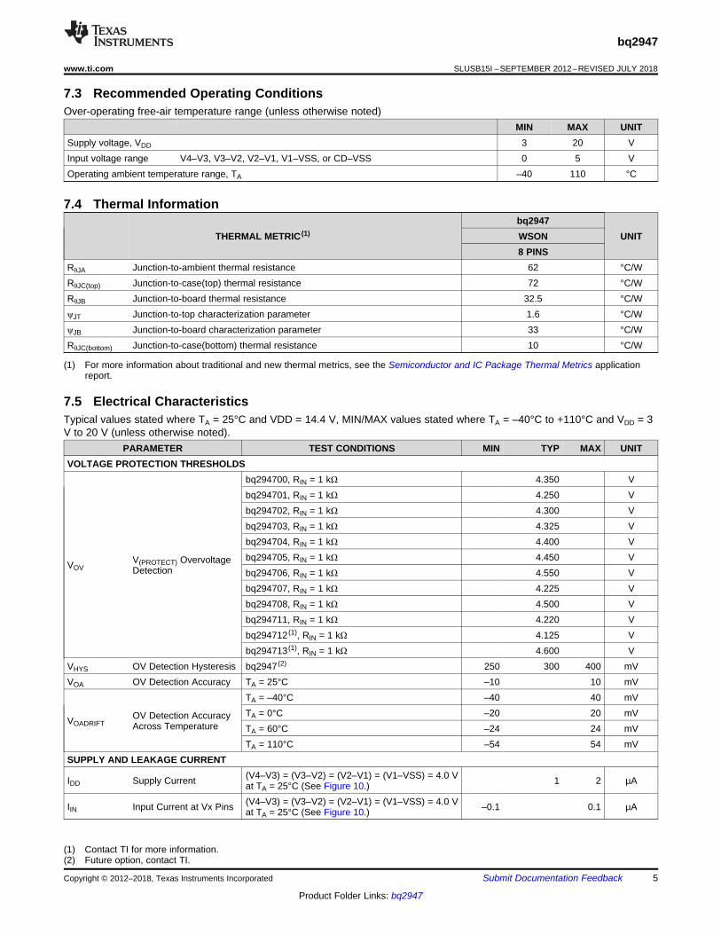
7.5 Electrical CharacteristicsTypical values stated where TA = 25°C and VDD = 14.4 V, MIN/MAX values stated where TA = –40°C to +110°C and VDD = 3V to 20 V (unless otherwise noted).
PARAMETER TEST CONDITIONS MIN TYP MAX UNITVOLTAGE PROTECTION THRESHOLDS
VOVV(PROTECT) OvervoltageDetection
bq294700, RIN = 1 kΩ 4.350 Vbq294701, RIN = 1 kΩ 4.250 Vbq294702, RIN = 1 kΩ 4.300 Vbq294703, RIN = 1 kΩ 4.325 Vbq294704, RIN = 1 kΩ 4.400 Vbq294705, RIN = 1 kΩ 4.450 Vbq294706, RIN = 1 kΩ 4.550 Vbq294707, RIN = 1 kΩ 4.225 Vbq294708, RIN = 1 kΩ 4.500 Vbq294711, RIN = 1 kΩ 4.220 Vbq294712 (1), RIN = 1 kΩ 4.125 Vbq294713 (1), RIN = 1 kΩ 4.600 V
VHYS OV Detection Hysteresis bq2947 (2) 250 300 400 mVVOA OV Detection Accuracy TA = 25°C –10 10 mV
VOADRIFTOV Detection AccuracyAcross Temperature
TA = –40°C –40 40 mVTA = 0°C –20 20 mVTA = 60°C –24 24 mVTA = 110°C –54 54 mV
SUPPLY AND LEAKAGE CURRENT
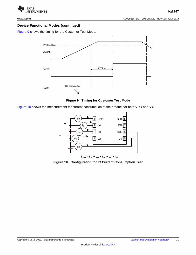
IDD Supply Current (V4–V3) = (V3–V2) = (V2–V1) = (V1–VSS) = 4.0 Vat TA = 25°C (See Figure 10.) 1 2 µA
IIN Input Current at Vx Pins (V4–V3) = (V3–V2) = (V2–V1) = (V1–VSS) = 4.0 Vat TA = 25°C (See Figure 10.) –0.1 0.1 µA
6
bq2947
SLUSB15I –SEPTEMBER 2012–REVISED JULY 2018 www.ti.com
Product Folder Links: bq2947
Submit Documentation Feedback Copyright © 2012–2018, Texas Instruments Incorporated
Electrical Characteristics (continued)Typical values stated where TA = 25°C and VDD = 14.4 V, MIN/MAX values stated where TA = –40°C to +110°C and VDD = 3V to 20 V (unless otherwise noted).
PARAMETER TEST CONDITIONS MIN TYP MAX UNIT
ICELLInput Current (ALL Vxand VDD Input Pins)
Current Consumption at Power down, (V4–V3) =(V3–V2) = (V2–V1) = (V1–VSS) = 2.30 V at TA =25°C
1.1 µA
OUTPUT DRIVE OUT, CMOS ACTIVE HIGH VERSIONS ONLY
VOUTOutput Drive Voltage,Active High
(V4–V3), (V3–V2), (V2–V1), or (V1–VSS) > VOV,VDD = 14.4 V, IOH = 100 µA 6 V
If three of four cells are short circuited, only onecell remains powered and > VOV, VDD = Vx (cellvoltage), IOH = 100 µA
VDD – 0.3 V
(V4–V3), (V3–V2), (V2–V1), and (V1–VSS) < VOV,VDD = 14.4 V, IOL = 100 µA measured into OUTpin.
250 400 mV
IOUTHOUT Source Current(during OV)
(V4–V3), (V3–V2), (V2–V1), or (V1–VSS) > VOV,VDD = 14.4 V,OUT = 0 V, measured out of OUT pin.
4.5 mA
IOUTLOUT Sink Current (noOV)
(V4–V3), (V3–V2), (V2–V1), and (V1–VSS) < VOV,VDD = 14.4 V,OUT = VDD, measured into OUT pin .Pull resistorRPU = 5 kΩ to VDD = 14.4 V
0.5 14 mA
OUTPUT DRIVE OUT, CMOS OPEN DRAIN ACTIVE LOW VERSIONS ONLY
VOUTOutput Drive Voltage,Active High
(V4–V3), (V3–V2), (V2–V1), and (V1–VSS) < VOV,VDD = 14.4 V, IOL = 100 µA measured into OUTpin.
250 400 mV
IOUTLOUT Sink Current (noOV)
(V4–V3), (V3–V2), (V2–V1), and (V1–VSS) < VOV,VDD = 14.4 V,OUT = VDD, measured into OUT pin. Pull resistorRPU = 5 kΩ to VDD = 14.4 V
0.5 14 mA
IOUTLK OUT pin leakage(V4–V3), (V3–V2), (V2–V1), and (V1–VSS) < VOV,VDD = 14.4 V,OUT = VDD, measured into OUT pin.
100 nA
DELAY TIMERtCD OV Delay Time CCD = 0.1 µF (see Equation 1) 1 1.5 2 s
tCD_GNDOV Delay Time with CDpin = 0 V
Delay due to CCD capacitor shorted to ground forCustomer Test Mode 20 170 ms
−3.88
−3.86
−3.84
−3.82
−3.80
−3.78
−3.76
−3.74
−3.72
−3.70
−3.68
−50 −25 0 25 50 75 100 125Temperature (°C)
I OU
T (
mA
)
G005
0
1
2
3
4
5
6
7
8
0 5 10 15 20 25 30VDD (V)
VO
UT (
V)
G006
0.6
0.7
0.8
0.9
1.0
1.1
1.2
1.3
1.4
1.5
1.6
−50 −25 0 25 50 75 100 125Temperature (°C)
I DD (
µA)
G003
0.6
0.8
1.0
1.2
1.4
1.6
1.8
−50 −25 0 25 50 75 100 125Temperature (°C)
I CE
LL (
µA)
G004
4.30
4.31
4.32
4.33
4.34
4.35
4.36
4.37
4.38
4.39
4.40
−50 −25 0 25 50 75 100 125Temperature (°C)
VO
UT (
V)
MeanMinMax
G001
0.312
0.313
0.314
0.315
0.316
−50 −25 0 25 50 75 100 125Temperature (°C)
VH
YS (
V)
G002
7
bq2947
www.ti.com SLUSB15I –SEPTEMBER 2012–REVISED JULY 2018
Product Folder Links: bq2947
Submit Documentation FeedbackCopyright © 2012–2018, Texas Instruments Incorporated
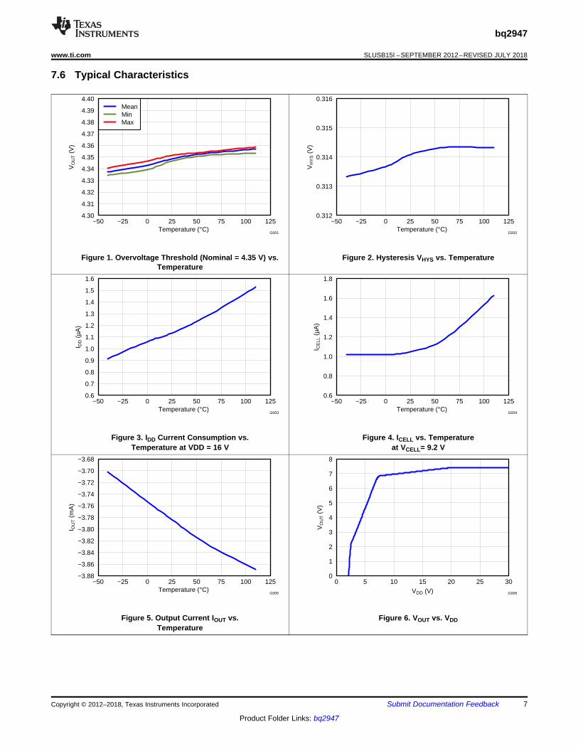
7.6 Typical Characteristics
Figure 1. Overvoltage Threshold (Nominal = 4.35 V) vs.Temperature
Figure 2. Hysteresis VHYS vs. Temperature
Figure 3. IDD Current Consumption vs.Temperature at VDD = 16 V
Figure 4. ICELL vs. Temperatureat VCELL= 9.2 V
Figure 5. Output Current IOUT vs.Temperature
Figure 6. VOUT vs. VDD
OUT
V4
V3
V1
V2
VSS
VDD
CD
PACK+
PACK–
RIN
CCD
CVD
RVD
VOV
8
79
1
2
3
4
5
6
PWPD
Se
nsin
g C
ircu
it
Enable
ActiveDelay Charge/Discharge Circuit
CIN
CIN
CIN
CIN
RIN
RIN
RIN
8
bq2947
SLUSB15I –SEPTEMBER 2012–REVISED JULY 2018 www.ti.com
Product Folder Links: bq2947
Submit Documentation Feedback Copyright © 2012–2018, Texas Instruments Incorporated
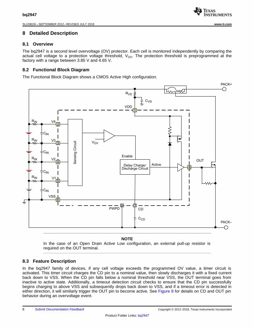
8 Detailed Description
8.1 OverviewThe bq2947 is a second level overvoltage (OV) protector. Each cell is monitored independently by comparing theactual cell voltage to a protection voltage threshold, VOV. The protection threshold is preprogrammed at thefactory with a range between 3.85 V and 4.65 V.
8.2 Functional Block DiagramThe Functional Block Diagram shows a CMOS Active High configuration.
NOTEIn the case of an Open Drain Active Low configuration, an external pull-up resistor isrequired on the OUT terminal.
8.3 Feature DescriptionIn the bq2947 family of devices, if any cell voltage exceeds the programmed OV value, a timer circuit isactivated. This timer circuit charges the CD pin to a nominal value, then slowly discharges it with a fixed currentback down to VSS. When the CD pin falls below a nominal threshold near VSS, the OUT terminal goes frominactive to active state. Additionally, a timeout detection circuit checks to ensure that the CD pin successfullybegins charging to above VSS and subsequently drops back down to VSS, and if a timeout error is detected ineither direction, it will similarly trigger the OUT pin to become active. See Figure 8 for details on CD and OUT pinbehavior during an overvoltage event.
VCD
Fault conditionpresent
tCHGDELAY
tCD
V(CD)
Fault responsebecomes active
VOUT1
V(OUT)
Note: Active High OUT version shown
VOV
VOV–VHYS
Ce
llV
olta
ge
( V)
V3
V2,
V2
V1,V
1–
VS
S)
OUT (V)tCD
––
3( V
4–
V3,
9
bq2947
www.ti.com SLUSB15I –SEPTEMBER 2012–REVISED JULY 2018
Product Folder Links: bq2947
Submit Documentation FeedbackCopyright © 2012–2018, Texas Instruments Incorporated
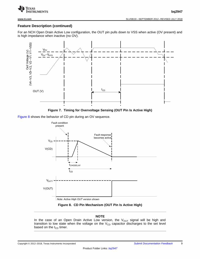
Feature Description (continued)For an NCH Open Drain Active Low configuration, the OUT pin pulls down to VSS when active (OV present) andis high impedance when inactive (no OV).
Figure 7. Timing for Overvoltage Sensing (OUT Pin Is Active High)
Figure 8 shows the behavior of CD pin during an OV sequence.
Figure 8. CD Pin Mechanism (OUT Pin Is Active High)
NOTEIn the case of an Open Drain Active Low version, the VOUT signal will be high andtransition to low state when the voltage on the VCD capacitor discharges to the set levelbased on the tCD timer.
10
bq2947
SLUSB15I –SEPTEMBER 2012–REVISED JULY 2018 www.ti.com
Product Folder Links: bq2947
Submit Documentation Feedback Copyright © 2012–2018, Texas Instruments Incorporated
Feature Description (continued)8.3.1 Pin Details
8.3.1.1 Input Sense Voltage, VxThese inputs sense each battery cell voltage. A series resistor and a capacitor across the cell for each input isrequired for noise filtering and stable voltage monitoring.
8.3.1.2 Output Drive, OUTThis terminal serves as the fault signal output, and may be ordered in either Active High or Open Drain ActiveLow options.
8.3.1.3 Supply Input, VDDThis terminal is the unregulated input power source for the IC. A series resistor is connected to limit the current,and a capacitor is connected to ground for noise filtering.
8.3.1.4 External Delay Capacitor, CDThis terminal is connected to an external capacitor that sets the delay timer during an overvoltage fault event.
The CD pin includes a timeout detection circuit to ensure that the output drives active even with a shorted oropen capacitor during an overvoltage event.
The capacitor connected on the CD pin rapidly charges to a voltage if any one of the cell inputs exceeds the OVthreshold. Then the delay circuit gradually discharges the capacitor on the CD pin. Once this capacitordischarges below a set voltage, the OUT transitions from an inactive to active state.
To calculate the delay, use the following equation:tCD (sec) = K × CCD (µF), where K = 10 to 20 range. (1)
Example: If CCD= 0.1 µF (typical), then the delay timer range is
tCD (s) = 10 × 0.1 = 1 s (Minimum)
tCD (s) = 20 × 0.1 = 2 s (Maximum)
NOTEThe tolerance on the capacitor used for CCD increases the range of the tCD timer.
8.4 Device Functional Modes
8.4.1 NORMAL ModeWhen all of the cell voltages are below the overvoltage threshold, VOV, the device operates in NORMAL mode.The device monitors the differential cell voltages connected across (V1–VSS), (V2–V1), (V3–V2), and (V4–V3).The OUT pin is inactive, and is low if configured active high, or, if configured active low, is an open drain beingexternally pulled up.
8.4.2 OVERVOLTAGE ModeOVERVOLTAGE mode is detected if any of the cell voltage exceeds the overvoltage threshold, VOV forconfigured OV delay time. The OUT pin is activated after a delay time set by the capacitance in the CD pin. TheOUT pin will either pull high internally, if configured as active high, or will be pulled low internally if configured asactive low. An external FET is then turned on, shorting the fuse to ground, which allows the battery and/orcharger power to blow the fuse. When all of the cell voltages fall below the (VOV–VHYS), the device returns toNORMAL mode.
8.4.3 Customer Test ModeIt is possible to reduce test time for checking the overvoltage function by simply shorting the external CDcapacitor to VSS. In this case, the OV delay would be reduced to the t(CD_GND) value, which has a maximum of170 ms.
OUTVDD
VSS
1
3
2
6
4 5
IIN4
I IN3
IIN2
IDD
V3
V1V2
7
8
V4
IIN1
CD
ICELL
ICELL = IDD + IIN1 + I IN2 + IIN3 + I IN4
V(OUT)
V(VCELL)
OV Condition
≤ 170 ms
V(CD)CD pin held low
11
bq2947
www.ti.com SLUSB15I –SEPTEMBER 2012–REVISED JULY 2018
Product Folder Links: bq2947
Submit Documentation FeedbackCopyright © 2012–2018, Texas Instruments Incorporated
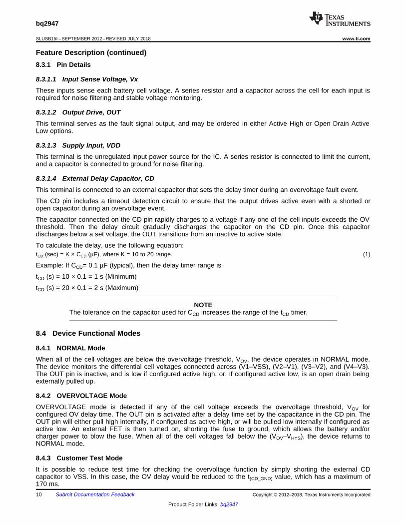
Device Functional Modes (continued)Figure 9 shows the timing for the Customer Test Mode.
Figure 9. Timing for Customer Test Mode
Figure 10 shows the measurement for current consumption of the product for both VDD and Vx.
Figure 10. Configuration for IC Current Consumption Test
100 Ω
VCELL1
VCELL3
VCELL2
OUTVDD
VSS
0.1 µF
1k
1k
Pack+
Pack–
V3
V2 V1
V4 CDVCELL4
PWPD
0.1 µF
0.1µF
0.1µF
0.1µF
1k
1k
0.1µF
Copyright © 2017, Texas Instruments Incorporated
12
bq2947
SLUSB15I –SEPTEMBER 2012–REVISED JULY 2018 www.ti.com
Product Folder Links: bq2947
Submit Documentation Feedback Copyright © 2012–2018, Texas Instruments Incorporated
9 Application and Implementation
NOTEInformation in the following applications sections is not part of the TI componentspecification, and TI does not warrant its accuracy or completeness. TI’s customers areresponsible for determining suitability of components for their purposes. Customers shouldvalidate and test their design implementation to confirm system functionality.
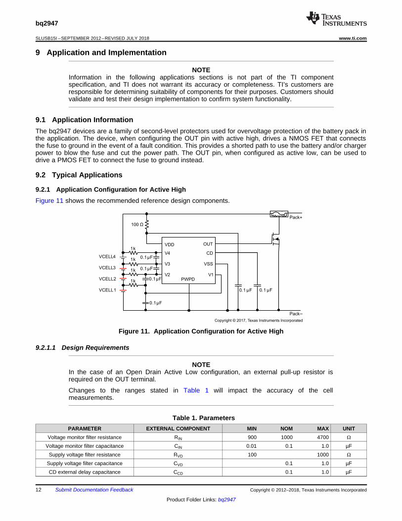
9.1 Application InformationThe bq2947 devices are a family of second-level protectors used for overvoltage protection of the battery pack inthe application. The device, when configuring the OUT pin with active high, drives a NMOS FET that connectsthe fuse to ground in the event of a fault condition. This provides a shorted path to use the battery and/or chargerpower to blow the fuse and cut the power path. The OUT pin, when configured as active low, can be used todrive a PMOS FET to connect the fuse to ground instead.
9.2 Typical Applications
9.2.1 Application Configuration for Active HighFigure 11 shows the recommended reference design components.
Figure 11. Application Configuration for Active High
9.2.1.1 Design Requirements
NOTEIn the case of an Open Drain Active Low configuration, an external pull-up resistor isrequired on the OUT terminal.
Changes to the ranges stated in Table 1 will impact the accuracy of the cellmeasurements.
Table 1. ParametersPARAMETER EXTERNAL COMPONENT MIN NOM MAX UNIT
Voltage monitor filter resistance RIN 900 1000 4700 Ω
Voltage monitor filter capacitance CIN 0.01 0.1 1.0 µFSupply voltage filter resistance RVD 100 1000 Ω
Supply voltage filter capacitance CVD 0.1 1.0 µFCD external delay capacitance CCD 0.1 1.0 µF
100 Ω
VCELL1
VCELL3
VCELL2
OUTVDD
VSS
0.1µF
0.1µF
1k
1k
1k
Pack+
Pack–
V3
V2 V1
V4 CD
PWPD
0.1µF0.1µF 0.1µF0.1µF
0.1µF
Copyright © 2017, Texas Instruments Incorporated
100 Ω
VCELL1
VCELL2
OUTVDD
VSS
0.1µF
0.1µF1k
1k
Pack+
Pack–
V3
V2 V1
V4 CD
PWPD
0.1µF 0.1µF
0.1µF
Copyright © 2017, Texas Instruments Incorporated
13
bq2947
www.ti.com SLUSB15I –SEPTEMBER 2012–REVISED JULY 2018
Product Folder Links: bq2947
Submit Documentation FeedbackCopyright © 2012–2018, Texas Instruments Incorporated
NOTEThe device is calibrated using an RIN value = 1 kΩ. Using a value other than thisrecommended value changes the accuracy of the cell voltage measurements and VOVtrigger level.
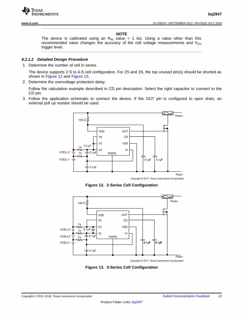
9.2.1.2 Detailed Design Procedure1. Determine the number of cell in series.
The device supports 2-S to 4-S cell configuration. For 2S and 3S, the top unused pin(s) should be shorted asshown in Figure 12 and Figure 13.
2. Determine the overvoltage protection delay.
Follow the calculation example described in CD pin description. Select the right capacitor to connect to theCD pin.
3. Follow the application schematic to connect the device. If the OUT pin is configured to open drain, anexternal pull up resistor should be used.
Figure 12. 2-Series Cell Configuration
Figure 13. 3-Series Cell Configuration
0.6
0.7
0.8
0.9
1.0
1.1
1.2
1.3
1.4
1.5
1.6
−50 −25 0 25 50 75 100 125Temperature (°C)
I DD (
µA)
G003
0
1
2
3
4
5
6
7
8
0 5 10 15 20 25 30VDD (V)
VO
UT (
V)
G006
4.30
4.31
4.32
4.33
4.34
4.35
4.36
4.37
4.38
4.39
4.40
−50 −25 0 25 50 75 100 125Temperature (°C)
VO
UT (
V)
MeanMinMax
G001
0.312
0.313
0.314
0.315
0.316
−50 −25 0 25 50 75 100 125Temperature (°C)
VH
YS (
V)
G002
14
bq2947
SLUSB15I –SEPTEMBER 2012–REVISED JULY 2018 www.ti.com
Product Folder Links: bq2947
Submit Documentation Feedback Copyright © 2012–2018, Texas Instruments Incorporated
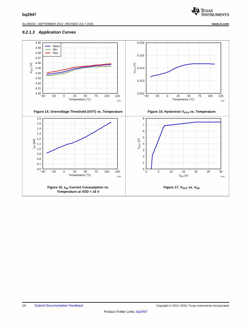
9.2.1.3 Application Curves
Figure 14. Overvoltage Threshold (OVT) vs. Temperature Figure 15. Hysteresis VHYS vs. Temperature
Figure 16. IDD Current Consumption vs.Temperature at VDD = 16 V
Figure 17. VOUT vs. VDD
VCELL1
VCELL3
VCELL2
OUTVDD Pack +
Pack -V3
V2 V1
V4 CD
VSSPWPD
Power Trace LinePlace the RC filters close to the
device terminals
Ensure trace can support sufficient currentflow for fuse blow
15
bq2947
www.ti.com SLUSB15I –SEPTEMBER 2012–REVISED JULY 2018
Product Folder Links: bq2947
Submit Documentation FeedbackCopyright © 2012–2018, Texas Instruments Incorporated
10 Power Supply RecommendationsThe maximum power of this device is 20 V on VDD.
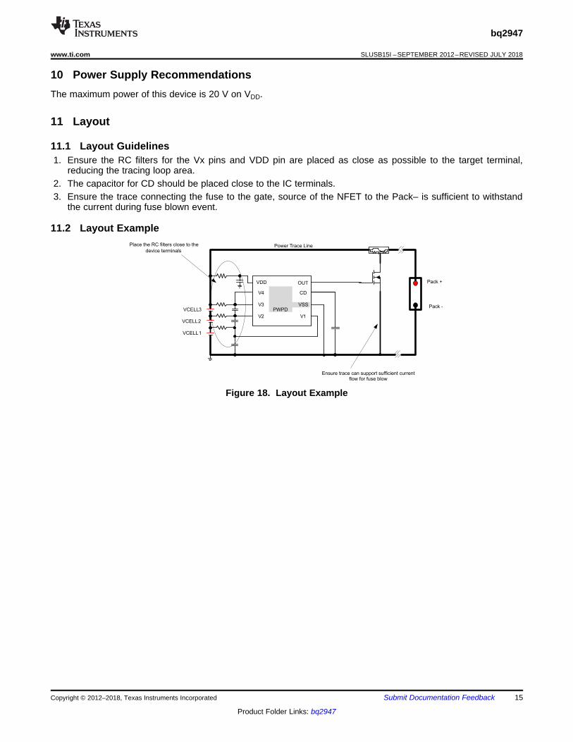
11 Layout
11.1 Layout Guidelines1. Ensure the RC filters for the Vx pins and VDD pin are placed as close as possible to the target terminal,
reducing the tracing loop area.2. The capacitor for CD should be placed close to the IC terminals.3. Ensure the trace connecting the fuse to the gate, source of the NFET to the Pack– is sufficient to withstand
the current during fuse blown event.
11.2 Layout Example
Figure 18. Layout Example
16
bq2947
SLUSB15I –SEPTEMBER 2012–REVISED JULY 2018 www.ti.com
Product Folder Links: bq2947
Submit Documentation Feedback Copyright © 2012–2018, Texas Instruments Incorporated
12 Device and Documentation Support
12.1 Documentation Support
12.1.1 Related DocumentationFor related documentation, see bq2945xy and bq2947xy Cascade Voltage Monitoring (SLUA662).
12.2 Receiving Notification of Documentation UpdatesTo receive notification of documentation updates, navigate to the device product folder on ti.com. In the upperright corner, click on Alert me to register and receive a weekly digest of any product information that haschanged. For change details, review the revision history included in any revised document.
12.3 Community ResourcesThe following links connect to TI community resources. Linked contents are provided "AS IS" by the respectivecontributors. They do not constitute TI specifications and do not necessarily reflect TI's views; see TI's Terms ofUse.
TI E2E™ Online Community TI's Engineer-to-Engineer (E2E) Community. Created to foster collaborationamong engineers. At e2e.ti.com, you can ask questions, share knowledge, explore ideas and helpsolve problems with fellow engineers.
Design Support TI's Design Support Quickly find helpful E2E forums along with design support tools andcontact information for technical support.
12.4 TrademarksPowerPAD, E2E are trademarks of Texas Instruments.All other trademarks are the property of their respective owners.
12.5 Electrostatic Discharge CautionThis integrated circuit can be damaged by ESD. Texas Instruments recommends that all integrated circuits be handled withappropriate precautions. Failure to observe proper handling and installation procedures can cause damage.
ESD damage can range from subtle performance degradation to complete device failure. Precision integrated circuits may be moresusceptible to damage because very small parametric changes could cause the device not to meet its published specifications.
12.6 GlossarySLYZ022 — TI Glossary.
This glossary lists and explains terms, acronyms, and definitions.
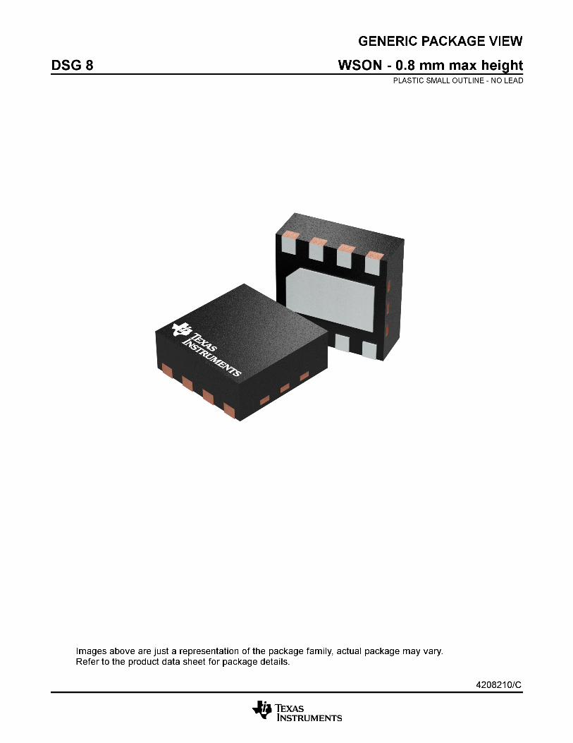
13 Mechanical, Packaging, and Orderable InformationThe following pages include mechanical, packaging, and orderable information. This information is the mostcurrent data available for the designated devices. This data is subject to change without notice and revision ofthis document. For browser-based versions of this data sheet, refer to the left-hand navigation.
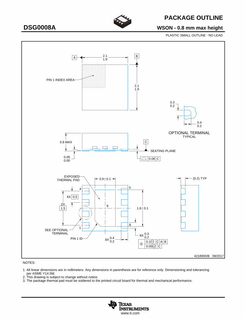
AA
www.ti.com
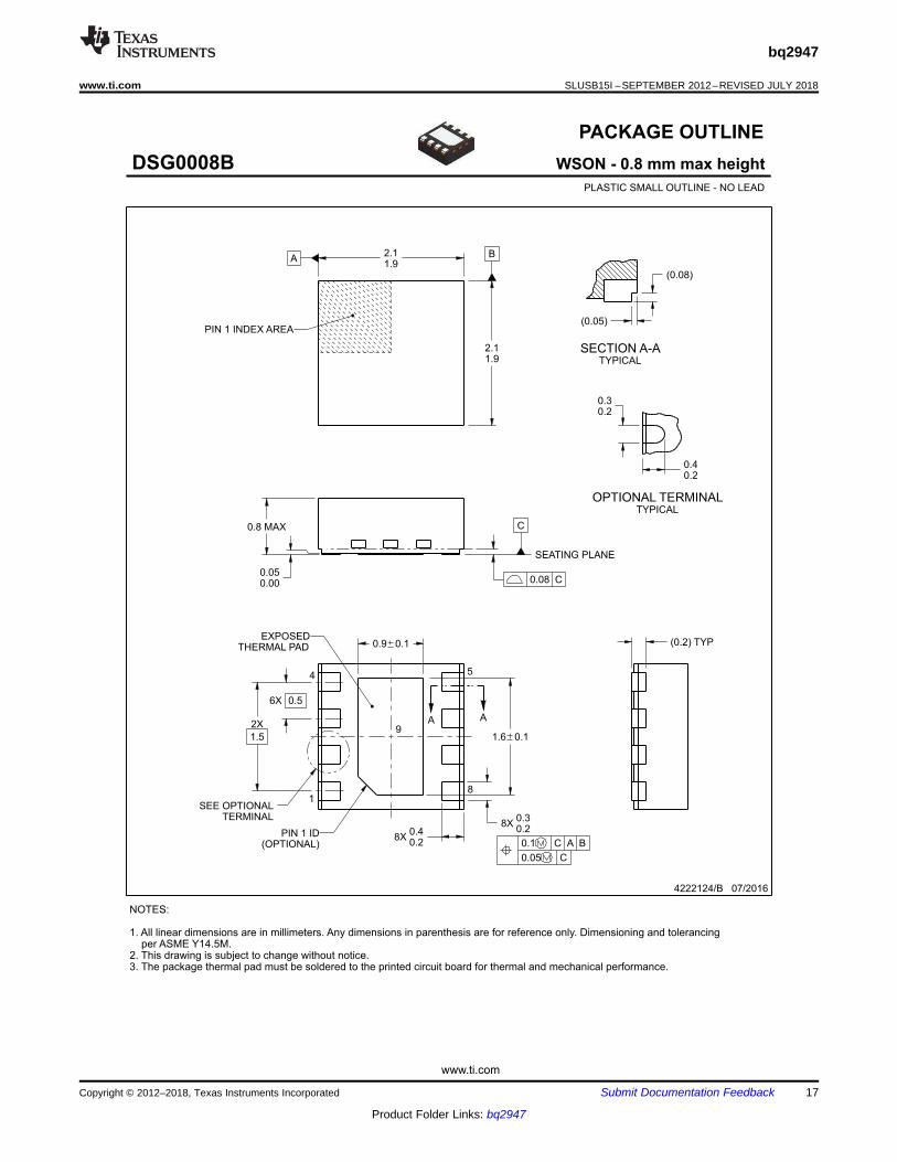
PACKAGE OUTLINE
C
SEE OPTIONALTERMINAL
8X0.30.2
1.6 0.1
2X
1.5
0.9 0.1
6X 0.5
8X0.40.2
0.050.00
0.8 MAX
A2.11.9
B
2.11.9
0.30.2
0.40.2
(0.2) TYP
(0.08)
(0.05)
WSON - 0.8 mm max heightDSG0008BPLASTIC SMALL OUTLINE - NO LEAD
4222124/B 07/2016
PIN 1 INDEX AREA
SEATING PLANE
0.08 C
1
4 5
8
(OPTIONAL)PIN 1 ID
0.1 C A B
0.05 C
THERMAL PADEXPOSED
9
NOTES:
1. All linear dimensions are in millimeters. Any dimensions in parenthesis are for reference only. Dimensioning and tolerancingper ASME Y14.5M.
2. This drawing is subject to change without notice.3. The package thermal pad must be soldered to the printed circuit board for thermal and mechanical performance.
SCALE 5.500
SCALE 30.000
SECTION A-A
SECTION A-A
OPTIONAL TERMINAL
TYPICAL
TYPICAL
17
bq2947
www.ti.com SLUSB15I –SEPTEMBER 2012–REVISED JULY 2018
Product Folder Links: bq2947
Submit Documentation FeedbackCopyright © 2012–2018, Texas Instruments Incorporated
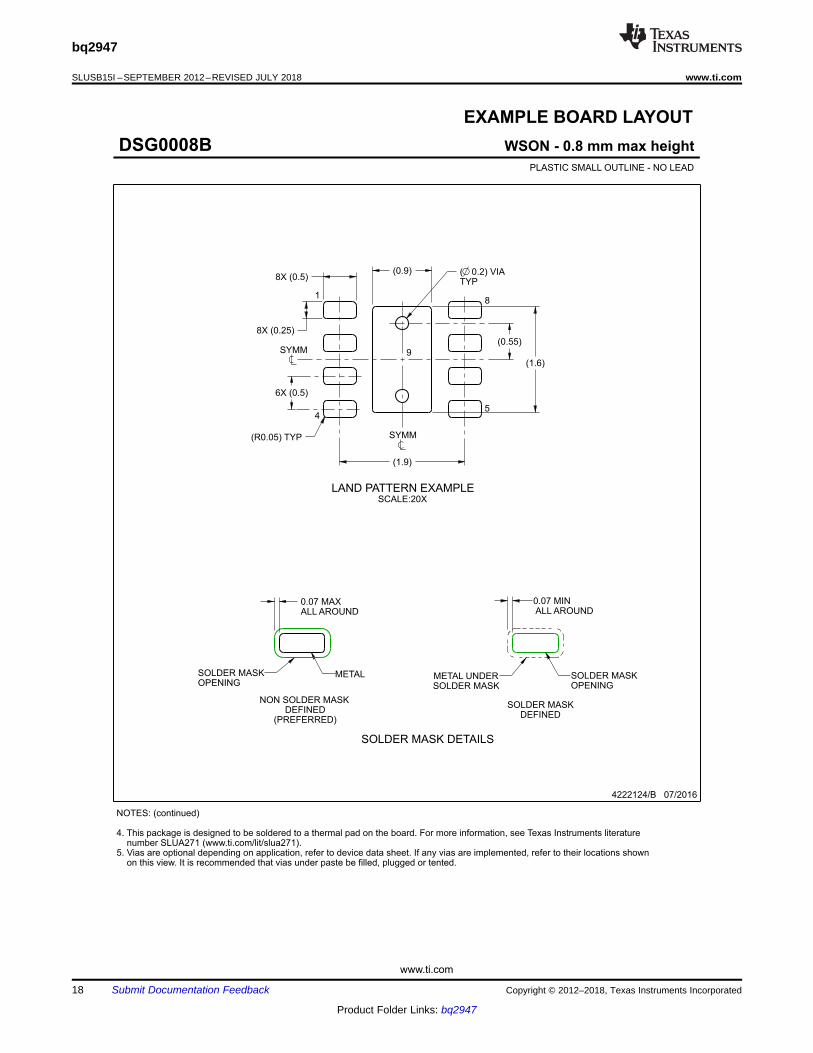
www.ti.com
EXAMPLE BOARD LAYOUT
0.07 MINALL AROUND
0.07 MAXALL AROUND
8X (0.25)
(1.6)
(1.9)
6X (0.5)
(0.9) ( 0.2) VIATYP
(0.55)
8X (0.5)
(R0.05) TYP
WSON - 0.8 mm max heightDSG0008BPLASTIC SMALL OUTLINE - NO LEAD
4222124/B 07/2016
SYMM
1
45
8
SCALE:20XLAND PATTERN EXAMPLE
SYMM 9
NOTES: (continued)
4. This package is designed to be soldered to a thermal pad on the board. For more information, see Texas Instruments literaturenumber SLUA271 (www.ti.com/lit/slua271).
5. Vias are optional depending on application, refer to device data sheet. If any vias are implemented, refer to their locations shownon this view. It is recommended that vias under paste be filled, plugged or tented.
SOLDER MASKOPENINGSOLDER MASK
METAL UNDER
SOLDER MASKDEFINED
METALSOLDER MASKOPENING
NON SOLDER MASK
SOLDER MASK DETAILS
DEFINED(PREFERRED)
18
bq2947
SLUSB15I –SEPTEMBER 2012–REVISED JULY 2018 www.ti.com
Product Folder Links: bq2947
Submit Documentation Feedback Copyright © 2012–2018, Texas Instruments Incorporated
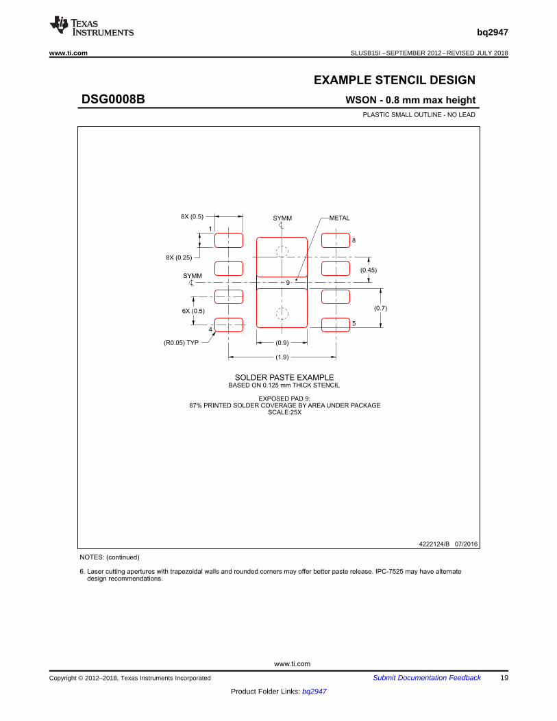
www.ti.com
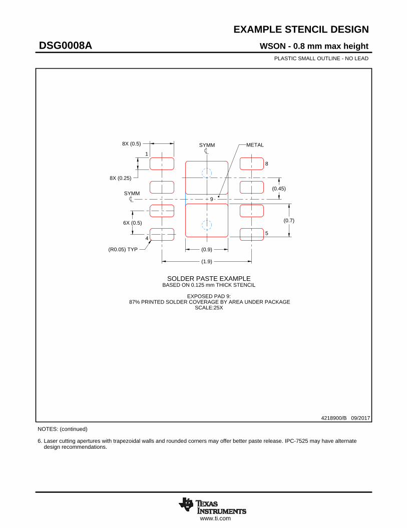
EXAMPLE STENCIL DESIGN
(R0.05) TYP
8X (0.25)
8X (0.5)
(0.9)
(0.7)
(1.9)
(0.45)
6X (0.5)
WSON - 0.8 mm max heightDSG0008BPLASTIC SMALL OUTLINE - NO LEAD
4222124/B 07/2016
NOTES: (continued)
6. Laser cutting apertures with trapezoidal walls and rounded corners may offer better paste release. IPC-7525 may have alternatedesign recommendations.
SOLDER PASTE EXAMPLEBASED ON 0.125 mm THICK STENCIL
EXPOSED PAD 9:87% PRINTED SOLDER COVERAGE BY AREA UNDER PACKAGE
SCALE:25X
SYMM
1
45
8
METAL
SYMM9
19
bq2947
www.ti.com SLUSB15I –SEPTEMBER 2012–REVISED JULY 2018
Product Folder Links: bq2947
Submit Documentation FeedbackCopyright © 2012–2018, Texas Instruments Incorporated
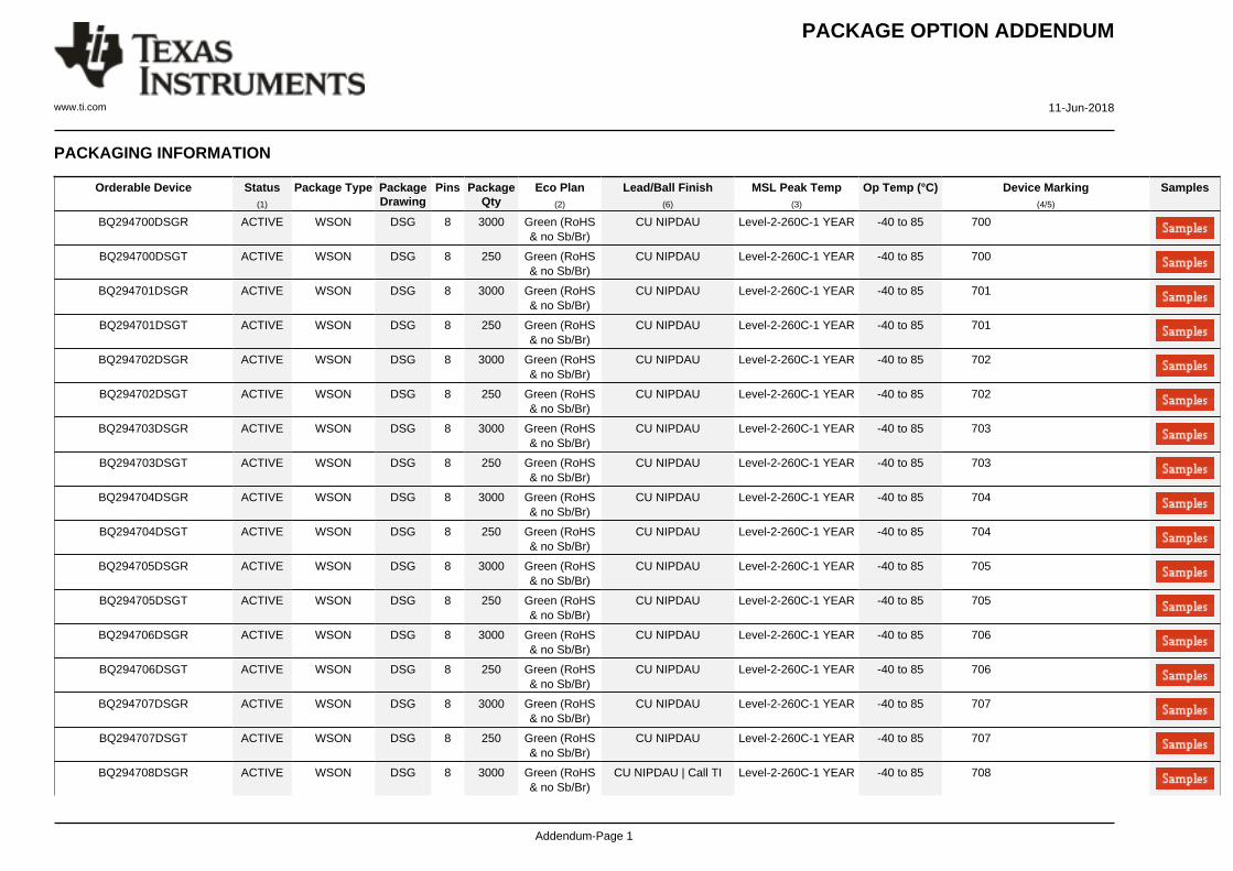
PACKAGE OPTION ADDENDUM
www.ti.com 11-Jun-2018
Addendum-Page 1
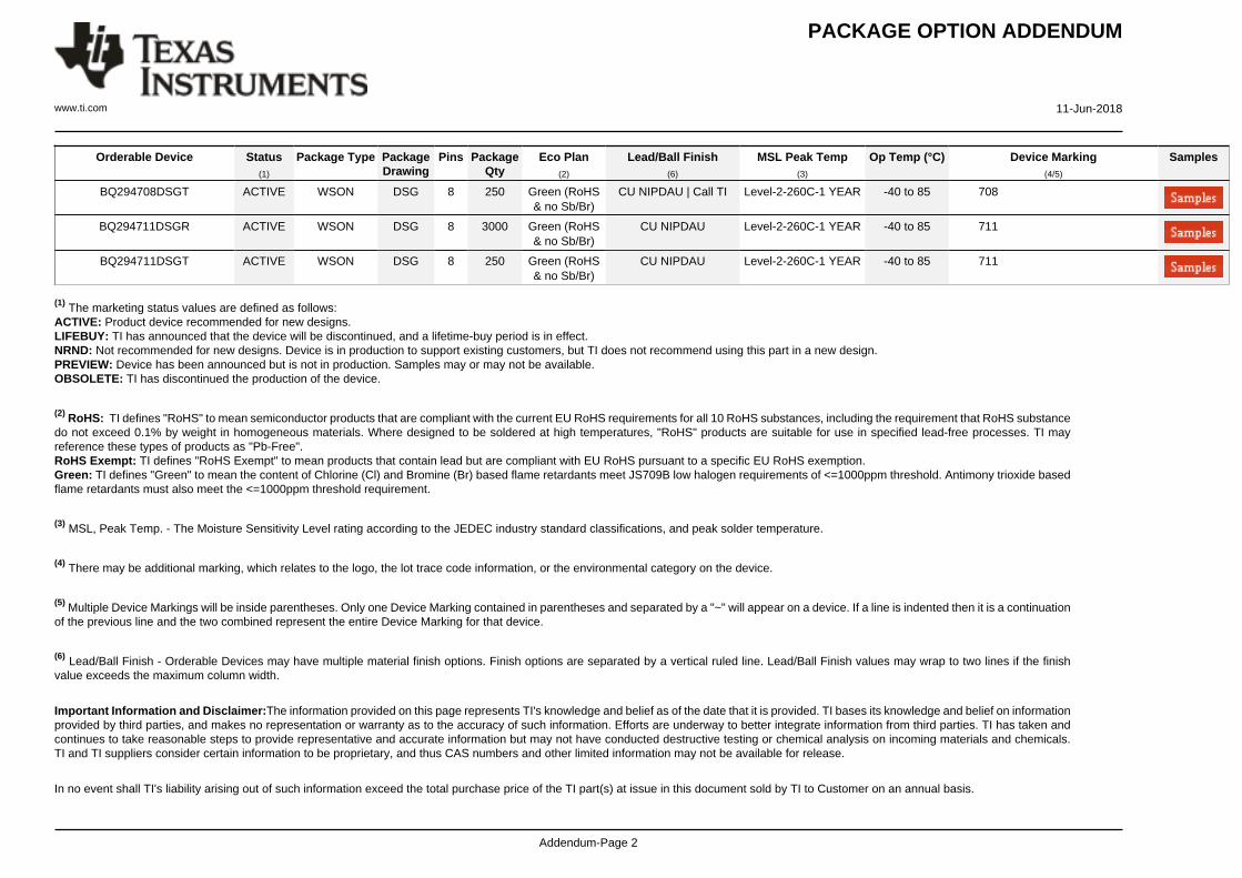
PACKAGING INFORMATION
Orderable Device Status(1)
Package Type PackageDrawing
Pins PackageQty
Eco Plan(2)
Lead/Ball Finish(6)
MSL Peak Temp(3)
Op Temp (°C) Device Marking(4/5)
Samples
BQ294700DSGR ACTIVE WSON DSG 8 3000 Green (RoHS& no Sb/Br)
CU NIPDAU Level-2-260C-1 YEAR -40 to 85 700
BQ294700DSGT ACTIVE WSON DSG 8 250 Green (RoHS& no Sb/Br)
CU NIPDAU Level-2-260C-1 YEAR -40 to 85 700
BQ294701DSGR ACTIVE WSON DSG 8 3000 Green (RoHS& no Sb/Br)
CU NIPDAU Level-2-260C-1 YEAR -40 to 85 701
BQ294701DSGT ACTIVE WSON DSG 8 250 Green (RoHS& no Sb/Br)
CU NIPDAU Level-2-260C-1 YEAR -40 to 85 701
BQ294702DSGR ACTIVE WSON DSG 8 3000 Green (RoHS& no Sb/Br)
CU NIPDAU Level-2-260C-1 YEAR -40 to 85 702
BQ294702DSGT ACTIVE WSON DSG 8 250 Green (RoHS& no Sb/Br)
CU NIPDAU Level-2-260C-1 YEAR -40 to 85 702
BQ294703DSGR ACTIVE WSON DSG 8 3000 Green (RoHS& no Sb/Br)
CU NIPDAU Level-2-260C-1 YEAR -40 to 85 703
BQ294703DSGT ACTIVE WSON DSG 8 250 Green (RoHS& no Sb/Br)
CU NIPDAU Level-2-260C-1 YEAR -40 to 85 703
BQ294704DSGR ACTIVE WSON DSG 8 3000 Green (RoHS& no Sb/Br)
CU NIPDAU Level-2-260C-1 YEAR -40 to 85 704
BQ294704DSGT ACTIVE WSON DSG 8 250 Green (RoHS& no Sb/Br)
CU NIPDAU Level-2-260C-1 YEAR -40 to 85 704
BQ294705DSGR ACTIVE WSON DSG 8 3000 Green (RoHS& no Sb/Br)
CU NIPDAU Level-2-260C-1 YEAR -40 to 85 705
BQ294705DSGT ACTIVE WSON DSG 8 250 Green (RoHS& no Sb/Br)
CU NIPDAU Level-2-260C-1 YEAR -40 to 85 705
BQ294706DSGR ACTIVE WSON DSG 8 3000 Green (RoHS& no Sb/Br)
CU NIPDAU Level-2-260C-1 YEAR -40 to 85 706
BQ294706DSGT ACTIVE WSON DSG 8 250 Green (RoHS& no Sb/Br)
CU NIPDAU Level-2-260C-1 YEAR -40 to 85 706
BQ294707DSGR ACTIVE WSON DSG 8 3000 Green (RoHS& no Sb/Br)
CU NIPDAU Level-2-260C-1 YEAR -40 to 85 707
BQ294707DSGT ACTIVE WSON DSG 8 250 Green (RoHS& no Sb/Br)
CU NIPDAU Level-2-260C-1 YEAR -40 to 85 707
BQ294708DSGR ACTIVE WSON DSG 8 3000 Green (RoHS& no Sb/Br)
CU NIPDAU | Call TI Level-2-260C-1 YEAR -40 to 85 708
PACKAGE OPTION ADDENDUM
www.ti.com 11-Jun-2018
Addendum-Page 2
Orderable Device Status(1)
Package Type PackageDrawing
Pins PackageQty
Eco Plan(2)
Lead/Ball Finish(6)
MSL Peak Temp(3)
Op Temp (°C) Device Marking(4/5)
Samples
BQ294708DSGT ACTIVE WSON DSG 8 250 Green (RoHS& no Sb/Br)
CU NIPDAU | Call TI Level-2-260C-1 YEAR -40 to 85 708
BQ294711DSGR ACTIVE WSON DSG 8 3000 Green (RoHS& no Sb/Br)
CU NIPDAU Level-2-260C-1 YEAR -40 to 85 711
BQ294711DSGT ACTIVE WSON DSG 8 250 Green (RoHS& no Sb/Br)
CU NIPDAU Level-2-260C-1 YEAR -40 to 85 711
(1) The marketing status values are defined as follows:ACTIVE: Product device recommended for new designs.LIFEBUY: TI has announced that the device will be discontinued, and a lifetime-buy period is in effect.NRND: Not recommended for new designs. Device is in production to support existing customers, but TI does not recommend using this part in a new design.PREVIEW: Device has been announced but is not in production. Samples may or may not be available.OBSOLETE: TI has discontinued the production of the device.
(2) RoHS: TI defines "RoHS" to mean semiconductor products that are compliant with the current EU RoHS requirements for all 10 RoHS substances, including the requirement that RoHS substancedo not exceed 0.1% by weight in homogeneous materials. Where designed to be soldered at high temperatures, "RoHS" products are suitable for use in specified lead-free processes. TI mayreference these types of products as "Pb-Free".RoHS Exempt: TI defines "RoHS Exempt" to mean products that contain lead but are compliant with EU RoHS pursuant to a specific EU RoHS exemption.Green: TI defines "Green" to mean the content of Chlorine (Cl) and Bromine (Br) based flame retardants meet JS709B low halogen requirements of <=1000ppm threshold. Antimony trioxide basedflame retardants must also meet the <=1000ppm threshold requirement.
(3) MSL, Peak Temp. - The Moisture Sensitivity Level rating according to the JEDEC industry standard classifications, and peak solder temperature.
(4) There may be additional marking, which relates to the logo, the lot trace code information, or the environmental category on the device.
(5) Multiple Device Markings will be inside parentheses. Only one Device Marking contained in parentheses and separated by a "~" will appear on a device. If a line is indented then it is a continuationof the previous line and the two combined represent the entire Device Marking for that device.
(6) Lead/Ball Finish - Orderable Devices may have multiple material finish options. Finish options are separated by a vertical ruled line. Lead/Ball Finish values may wrap to two lines if the finishvalue exceeds the maximum column width.
Important Information and Disclaimer:The information provided on this page represents TI's knowledge and belief as of the date that it is provided. TI bases its knowledge and belief on informationprovided by third parties, and makes no representation or warranty as to the accuracy of such information. Efforts are underway to better integrate information from third parties. TI has taken andcontinues to take reasonable steps to provide representative and accurate information but may not have conducted destructive testing or chemical analysis on incoming materials and chemicals.TI and TI suppliers consider certain information to be proprietary, and thus CAS numbers and other limited information may not be available for release.
In no event shall TI's liability arising out of such information exceed the total purchase price of the TI part(s) at issue in this document sold by TI to Customer on an annual basis.
PACKAGE OPTION ADDENDUM
www.ti.com 11-Jun-2018
Addendum-Page 3
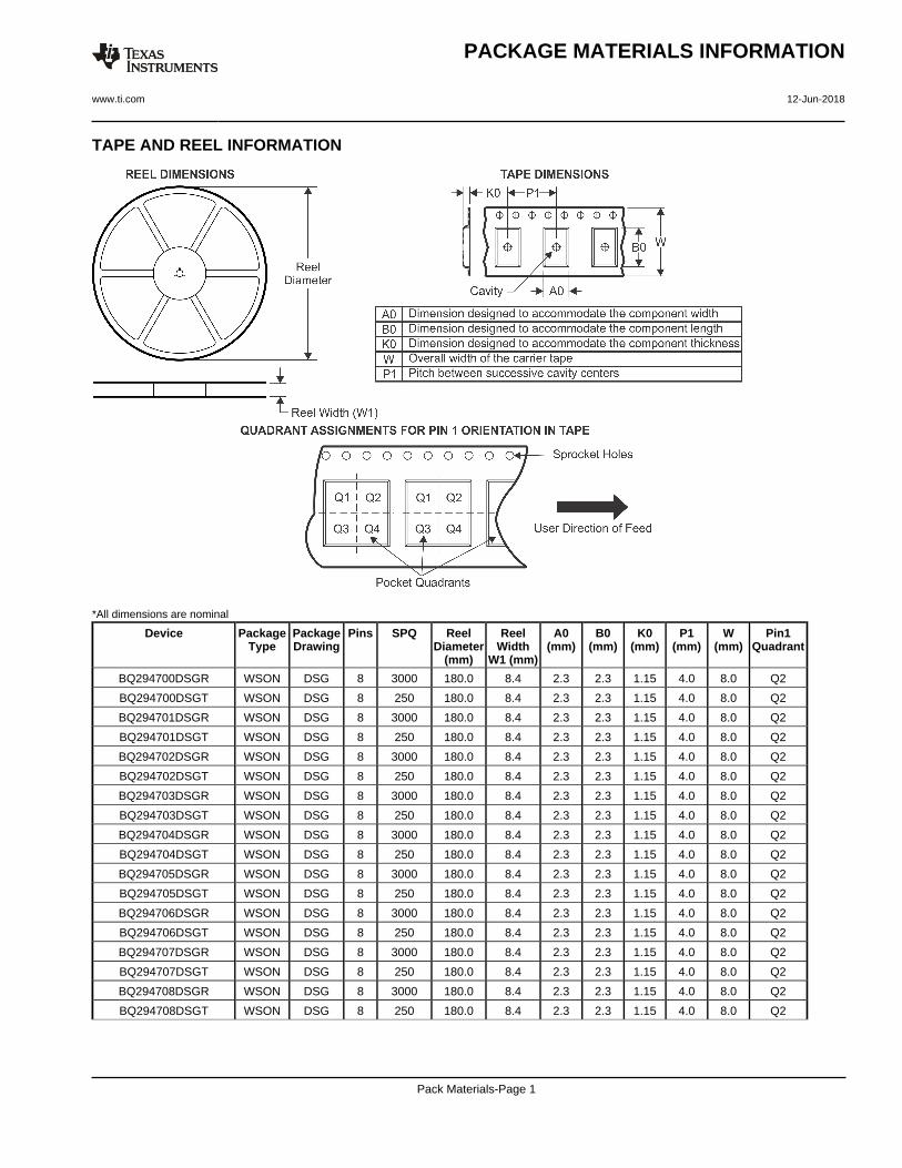
TAPE AND REEL INFORMATION
*All dimensions are nominal
Device PackageType
PackageDrawing
Pins SPQ ReelDiameter
(mm)
ReelWidth
W1 (mm)
A0(mm)
B0(mm)
K0(mm)
P1(mm)
W(mm)
Pin1Quadrant
BQ294700DSGR WSON DSG 8 3000 180.0 8.4 2.3 2.3 1.15 4.0 8.0 Q2
BQ294700DSGT WSON DSG 8 250 180.0 8.4 2.3 2.3 1.15 4.0 8.0 Q2
BQ294701DSGR WSON DSG 8 3000 180.0 8.4 2.3 2.3 1.15 4.0 8.0 Q2
BQ294701DSGT WSON DSG 8 250 180.0 8.4 2.3 2.3 1.15 4.0 8.0 Q2
BQ294702DSGR WSON DSG 8 3000 180.0 8.4 2.3 2.3 1.15 4.0 8.0 Q2
BQ294702DSGT WSON DSG 8 250 180.0 8.4 2.3 2.3 1.15 4.0 8.0 Q2
BQ294703DSGR WSON DSG 8 3000 180.0 8.4 2.3 2.3 1.15 4.0 8.0 Q2
BQ294703DSGT WSON DSG 8 250 180.0 8.4 2.3 2.3 1.15 4.0 8.0 Q2
BQ294704DSGR WSON DSG 8 3000 180.0 8.4 2.3 2.3 1.15 4.0 8.0 Q2
BQ294704DSGT WSON DSG 8 250 180.0 8.4 2.3 2.3 1.15 4.0 8.0 Q2
BQ294705DSGR WSON DSG 8 3000 180.0 8.4 2.3 2.3 1.15 4.0 8.0 Q2
BQ294705DSGT WSON DSG 8 250 180.0 8.4 2.3 2.3 1.15 4.0 8.0 Q2
BQ294706DSGR WSON DSG 8 3000 180.0 8.4 2.3 2.3 1.15 4.0 8.0 Q2
BQ294706DSGT WSON DSG 8 250 180.0 8.4 2.3 2.3 1.15 4.0 8.0 Q2
BQ294707DSGR WSON DSG 8 3000 180.0 8.4 2.3 2.3 1.15 4.0 8.0 Q2
BQ294707DSGT WSON DSG 8 250 180.0 8.4 2.3 2.3 1.15 4.0 8.0 Q2
BQ294708DSGR WSON DSG 8 3000 180.0 8.4 2.3 2.3 1.15 4.0 8.0 Q2
BQ294708DSGT WSON DSG 8 250 180.0 8.4 2.3 2.3 1.15 4.0 8.0 Q2
PACKAGE MATERIALS INFORMATION
www.ti.com 12-Jun-2018
Pack Materials-Page 1
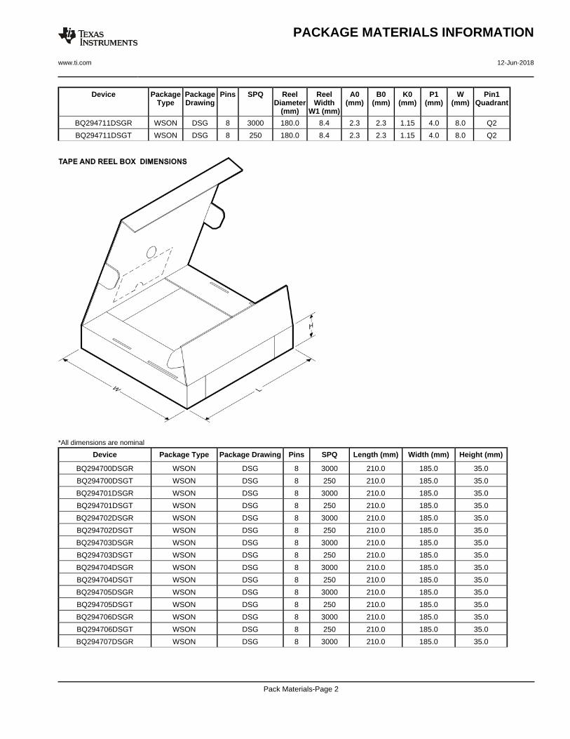
Device PackageType
PackageDrawing
Pins SPQ ReelDiameter
(mm)
ReelWidth
W1 (mm)
A0(mm)
B0(mm)
K0(mm)
P1(mm)
W(mm)
Pin1Quadrant
BQ294711DSGR WSON DSG 8 3000 180.0 8.4 2.3 2.3 1.15 4.0 8.0 Q2
BQ294711DSGT WSON DSG 8 250 180.0 8.4 2.3 2.3 1.15 4.0 8.0 Q2
*All dimensions are nominal
Device Package Type Package Drawing Pins SPQ Length (mm) Width (mm) Height (mm)
BQ294700DSGR WSON DSG 8 3000 210.0 185.0 35.0
BQ294700DSGT WSON DSG 8 250 210.0 185.0 35.0
BQ294701DSGR WSON DSG 8 3000 210.0 185.0 35.0
BQ294701DSGT WSON DSG 8 250 210.0 185.0 35.0
BQ294702DSGR WSON DSG 8 3000 210.0 185.0 35.0
BQ294702DSGT WSON DSG 8 250 210.0 185.0 35.0
BQ294703DSGR WSON DSG 8 3000 210.0 185.0 35.0
BQ294703DSGT WSON DSG 8 250 210.0 185.0 35.0
BQ294704DSGR WSON DSG 8 3000 210.0 185.0 35.0
BQ294704DSGT WSON DSG 8 250 210.0 185.0 35.0
BQ294705DSGR WSON DSG 8 3000 210.0 185.0 35.0
BQ294705DSGT WSON DSG 8 250 210.0 185.0 35.0
BQ294706DSGR WSON DSG 8 3000 210.0 185.0 35.0
BQ294706DSGT WSON DSG 8 250 210.0 185.0 35.0
BQ294707DSGR WSON DSG 8 3000 210.0 185.0 35.0
PACKAGE MATERIALS INFORMATION
www.ti.com 12-Jun-2018
Pack Materials-Page 2
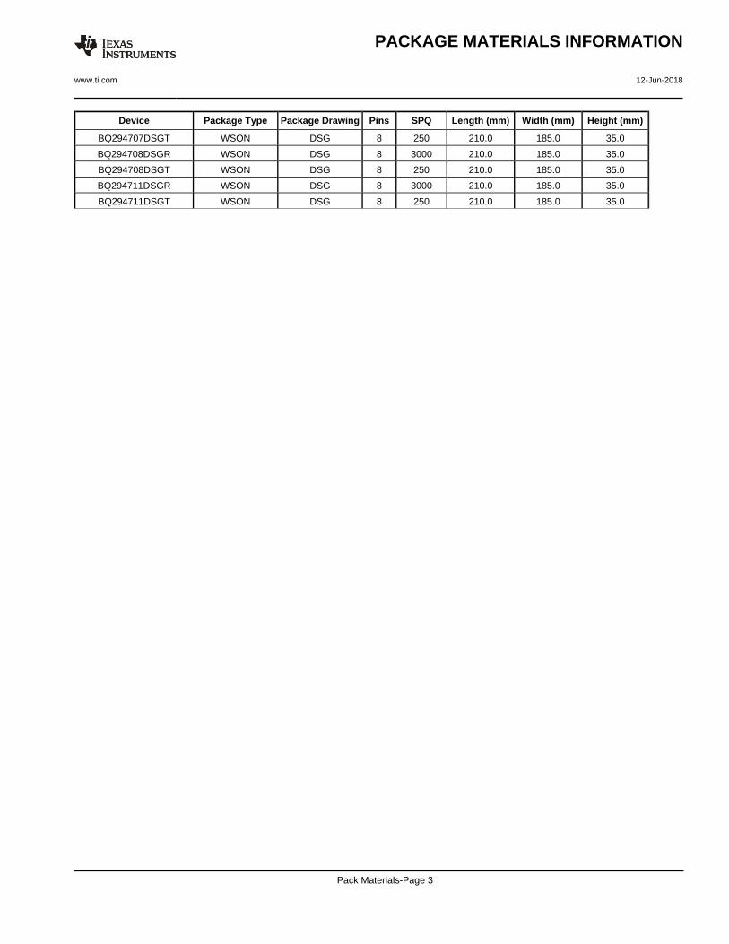
Device Package Type Package Drawing Pins SPQ Length (mm) Width (mm) Height (mm)
BQ294707DSGT WSON DSG 8 250 210.0 185.0 35.0
BQ294708DSGR WSON DSG 8 3000 210.0 185.0 35.0
BQ294708DSGT WSON DSG 8 250 210.0 185.0 35.0
BQ294711DSGR WSON DSG 8 3000 210.0 185.0 35.0
BQ294711DSGT WSON DSG 8 250 210.0 185.0 35.0
PACKAGE MATERIALS INFORMATION
www.ti.com 12-Jun-2018
Pack Materials-Page 3
www.ti.com
PACKAGE OUTLINE
C
SEE OPTIONALTERMINAL 8X 0.3
0.2
1.6 0.12X1.5
0.9 0.1
6X 0.5
8X 0.40.2
0.050.00
0.8 MAX
A 2.11.9
B
2.11.9
0.30.2
0.40.2
(0.2) TYP
WSON - 0.8 mm max heightDSG0008APLASTIC SMALL OUTLINE - NO LEAD
4218900/B 09/2017
PIN 1 INDEX AREA
SEATING PLANE
0.08 C
1
4 5
8
PIN 1 ID0.1 C A B0.05 C
THERMAL PADEXPOSED
9
NOTES: 1. All linear dimensions are in millimeters. Any dimensions in parenthesis are for reference only. Dimensioning and tolerancing per ASME Y14.5M. 2. This drawing is subject to change without notice. 3. The package thermal pad must be soldered to the printed circuit board for thermal and mechanical performance.
SCALE 5.500
OPTIONAL TERMINALTYPICAL
www.ti.com
EXAMPLE BOARD LAYOUT
0.07 MINALL AROUND
0.07 MAXALL AROUND
8X (0.25)
(1.6)
(1.9)
6X (0.5)
(0.9) ( 0.2) VIATYP
(0.55)
8X (0.5)
(R0.05) TYP
WSON - 0.8 mm max heightDSG0008APLASTIC SMALL OUTLINE - NO LEAD
4218900/B 09/2017
SYMM
1
45
8
LAND PATTERN EXAMPLESCALE:20X
SYMM 9
NOTES: (continued) 4. This package is designed to be soldered to a thermal pad on the board. For more information, see Texas Instruments literature number SLUA271 (www.ti.com/lit/slua271).5. Vias are optional depending on application, refer to device data sheet. If any vias are implemented, refer to their locations shown on this view. It is recommended that vias under paste be filled, plugged or tented.
SOLDER MASKOPENINGSOLDER MASK
METAL UNDER
SOLDER MASKDEFINED
METALSOLDER MASKOPENING
SOLDER MASK DETAILS
NON SOLDER MASKDEFINED
(PREFERRED)
www.ti.com
EXAMPLE STENCIL DESIGN
(R0.05) TYP
8X (0.25)
8X (0.5)
(0.9)
(0.7)
(1.9)
(0.45)
6X (0.5)
WSON - 0.8 mm max heightDSG0008APLASTIC SMALL OUTLINE - NO LEAD
4218900/B 09/2017
NOTES: (continued) 6. Laser cutting apertures with trapezoidal walls and rounded corners may offer better paste release. IPC-7525 may have alternate design recommendations.
SOLDER PASTE EXAMPLEBASED ON 0.125 mm THICK STENCIL
EXPOSED PAD 9:
87% PRINTED SOLDER COVERAGE BY AREA UNDER PACKAGESCALE:25X
SYMM
1
45
8
METAL
SYMM9
IMPORTANT NOTICE
Texas Instruments Incorporated (TI) reserves the right to make corrections, enhancements, improvements and other changes to itssemiconductor products and services per JESD46, latest issue, and to discontinue any product or service per JESD48, latest issue. Buyersshould obtain the latest relevant information before placing orders and should verify that such information is current and complete.TI’s published terms of sale for semiconductor products (http://www.ti.com/sc/docs/stdterms.htm) apply to the sale of packaged integratedcircuit products that TI has qualified and released to market. Additional terms may apply to the use or sale of other types of TI products andservices.Reproduction of significant portions of TI information in TI data sheets is permissible only if reproduction is without alteration and isaccompanied by all associated warranties, conditions, limitations, and notices. TI is not responsible or liable for such reproduceddocumentation. Information of third parties may be subject to additional restrictions. Resale of TI products or services with statementsdifferent from or beyond the parameters stated by TI for that product or service voids all express and any implied warranties for theassociated TI product or service and is an unfair and deceptive business practice. TI is not responsible or liable for any such statements.Buyers and others who are developing systems that incorporate TI products (collectively, “Designers”) understand and agree that Designersremain responsible for using their independent analysis, evaluation and judgment in designing their applications and that Designers havefull and exclusive responsibility to assure the safety of Designers' applications and compliance of their applications (and of all TI productsused in or for Designers’ applications) with all applicable regulations, laws and other applicable requirements. Designer represents that, withrespect to their applications, Designer has all the necessary expertise to create and implement safeguards that (1) anticipate dangerousconsequences of failures, (2) monitor failures and their consequences, and (3) lessen the likelihood of failures that might cause harm andtake appropriate actions. Designer agrees that prior to using or distributing any applications that include TI products, Designer willthoroughly test such applications and the functionality of such TI products as used in such applications.TI’s provision of technical, application or other design advice, quality characterization, reliability data or other services or information,including, but not limited to, reference designs and materials relating to evaluation modules, (collectively, “TI Resources”) are intended toassist designers who are developing applications that incorporate TI products; by downloading, accessing or using TI Resources in anyway, Designer (individually or, if Designer is acting on behalf of a company, Designer’s company) agrees to use any particular TI Resourcesolely for this purpose and subject to the terms of this Notice.TI’s provision of TI Resources does not expand or otherwise alter TI’s applicable published warranties or warranty disclaimers for TIproducts, and no additional obligations or liabilities arise from TI providing such TI Resources. TI reserves the right to make corrections,enhancements, improvements and other changes to its TI Resources. TI has not conducted any testing other than that specificallydescribed in the published documentation for a particular TI Resource.Designer is authorized to use, copy and modify any individual TI Resource only in connection with the development of applications thatinclude the TI product(s) identified in such TI Resource. NO OTHER LICENSE, EXPRESS OR IMPLIED, BY ESTOPPEL OR OTHERWISETO ANY OTHER TI INTELLECTUAL PROPERTY RIGHT, AND NO LICENSE TO ANY TECHNOLOGY OR INTELLECTUAL PROPERTYRIGHT OF TI OR ANY THIRD PARTY IS GRANTED HEREIN, including but not limited to any patent right, copyright, mask work right, orother intellectual property right relating to any combination, machine, or process in which TI products or services are used. Informationregarding or referencing third-party products or services does not constitute a license to use such products or services, or a warranty orendorsement thereof. Use of TI Resources may require a license from a third party under the patents or other intellectual property of thethird party, or a license from TI under the patents or other intellectual property of TI.TI RESOURCES ARE PROVIDED “AS IS” AND WITH ALL FAULTS. TI DISCLAIMS ALL OTHER WARRANTIES ORREPRESENTATIONS, EXPRESS OR IMPLIED, REGARDING RESOURCES OR USE THEREOF, INCLUDING BUT NOT LIMITED TOACCURACY OR COMPLETENESS, TITLE, ANY EPIDEMIC FAILURE WARRANTY AND ANY IMPLIED WARRANTIES OFMERCHANTABILITY, FITNESS FOR A PARTICULAR PURPOSE, AND NON-INFRINGEMENT OF ANY THIRD PARTY INTELLECTUALPROPERTY RIGHTS. TI SHALL NOT BE LIABLE FOR AND SHALL NOT DEFEND OR INDEMNIFY DESIGNER AGAINST ANY CLAIM,INCLUDING BUT NOT LIMITED TO ANY INFRINGEMENT CLAIM THAT RELATES TO OR IS BASED ON ANY COMBINATION OFPRODUCTS EVEN IF DESCRIBED IN TI RESOURCES OR OTHERWISE. IN NO EVENT SHALL TI BE LIABLE FOR ANY ACTUAL,DIRECT, SPECIAL, COLLATERAL, INDIRECT, PUNITIVE, INCIDENTAL, CONSEQUENTIAL OR EXEMPLARY DAMAGES INCONNECTION WITH OR ARISING OUT OF TI RESOURCES OR USE THEREOF, AND REGARDLESS OF WHETHER TI HAS BEENADVISED OF THE POSSIBILITY OF SUCH DAMAGES.Unless TI has explicitly designated an individual product as meeting the requirements of a particular industry standard (e.g., ISO/TS 16949and ISO 26262), TI is not responsible for any failure to meet such industry standard requirements.Where TI specifically promotes products as facilitating functional safety or as compliant with industry functional safety standards, suchproducts are intended to help enable customers to design and create their own applications that meet applicable functional safety standardsand requirements. Using products in an application does not by itself establish any safety features in the application. Designers mustensure compliance with safety-related requirements and standards applicable to their applications. Designer may not use any TI products inlife-critical medical equipment unless authorized officers of the parties have executed a special contract specifically governing such use.Life-critical medical equipment is medical equipment where failure of such equipment would cause serious bodily injury or death (e.g., lifesupport, pacemakers, defibrillators, heart pumps, neurostimulators, and implantables). Such equipment includes, without limitation, allmedical devices identified by the U.S. Food and Drug Administration as Class III devices and equivalent classifications outside the U.S.TI may expressly designate certain products as completing a particular qualification (e.g., Q100, Military Grade, or Enhanced Product).Designers agree that it has the necessary expertise to select the product with the appropriate qualification designation for their applicationsand that proper product selection is at Designers’ own risk. Designers are solely responsible for compliance with all legal and regulatoryrequirements in connection with such selection.Designer will fully indemnify TI and its representatives against any damages, costs, losses, and/or liabilities arising out of Designer’s non-compliance with the terms and provisions of this Notice.
Mailing Address: Texas Instruments, Post Office Box 655303, Dallas, Texas 75265Copyright © 2018, Texas Instruments Incorporated