BIPOLAR JUNCTION TRANSISTORS - Home | University … · BIPOLAR JUNCTION TRANSISTORS - GENERAL USE...
9
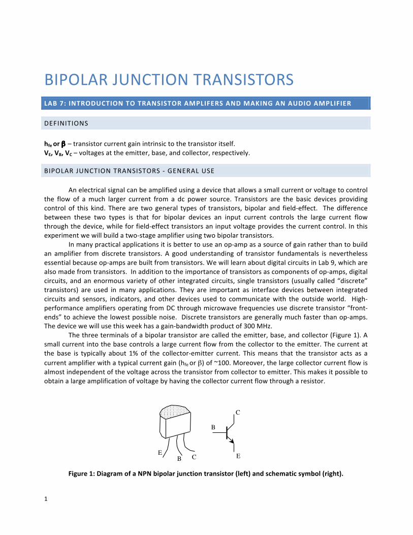
1 BIPOLAR JUNCTION TRANSISTORS LAB 7: INTRODUCTION TO TRANSISTOR AMPLIFERS AND MAKING AN AUDIO AMPLIFIER DEFINITIONS h fe or β – transistor current gain intrinsic to the transistor itself. V E ,V B ,V C – voltages at the emitter, base, and collector, respectively. BIPOLAR JUNCTION TRANSISTORS - GENERAL USE An electrical signal can be amplified using a device that allows a small current or voltage to control the flow of a much larger current from a dc power source. Transistors are the basic devices providing control of this kind. There are two general types of transistors, bipolar and field-effect. The difference between these two types is that for bipolar devices an input current controls the large current flow through the device, while for field-effect transistors an input voltage provides the current control. In this experiment we will build a two-stage amplifier using two bipolar transistors. In many practical applications it is better to use an op-amp as a source of gain rather than to build an amplifier from discrete transistors. A good understanding of transistor fundamentals is nevertheless essential because op-amps are built from transistors. We will learn about digital circuits in Lab 9, which are also made from transistors. In addition to the importance of transistors as components of op-amps, digital circuits, and an enormous variety of other integrated circuits, single transistors (usually called “discrete” transistors) are used in many applications. They are important as interface devices between integrated circuits and sensors, indicators, and other devices used to communicate with the outside world. High- performance amplifiers operating from DC through microwave frequencies use discrete transistor “front- ends” to achieve the lowest possible noise. Discrete transistors are generally much faster than op-amps. The device we will use this week has a gain-bandwidth product of 300 MHz. The three terminals of a bipolar transistor are called the emitter, base, and collector (Figure 1). A small current into the base controls a large current flow from the collector to the emitter. The current at the base is typically about 1% of the collector-emitter current. This means that the transistor acts as a current amplifier with a typical current gain (h fe or β) of ~100. Moreover, the large collector current flow is almost independent of the voltage across the transistor from collector to emitter. This makes it possible to obtain a large amplification of voltage by having the collector current flow through a resistor. Figure 1: Diagram of a NPN bipolar junction transistor (left) and schematic symbol (right). E B C E B C
Transcript of BIPOLAR JUNCTION TRANSISTORS - Home | University … · BIPOLAR JUNCTION TRANSISTORS - GENERAL USE...
1
BIPOLARJUNCTIONTRANSISTORSLAB7:INTRODUCTIONTOTRANSISTORAMPLIFERSANDMAKINGANAUDIOAMPLIFIER
DEFINITIONShfeorβ –transistorcurrentgainintrinsictothetransistoritself.VE,VB,VC–voltagesattheemitter,base,andcollector,respectively.
BIPOLARJUNCTIONTRANSISTORS-GENERALUSE Anelectricalsignalcanbeamplifiedusingadevicethatallowsasmallcurrentorvoltagetocontrolthe flow of amuch larger current from a dc power source. Transistors are the basic devices providingcontrol of this kind. There are two general types of transistors, bipolar and field-effect. The differencebetween these two types is that for bipolar devices an input current controls the large current flowthroughthedevice,whileforfield-effecttransistorsaninputvoltageprovidesthecurrentcontrol. Inthisexperimentwewillbuildatwo-stageamplifierusingtwobipolartransistors. Inmanypracticalapplicationsitisbettertouseanop-ampasasourceofgainratherthantobuildan amplifier from discrete transistors. A good understanding of transistor fundamentals is neverthelessessentialbecauseop-ampsarebuiltfromtransistors.WewilllearnaboutdigitalcircuitsinLab9,whicharealsomadefromtransistors.Inadditiontotheimportanceoftransistorsascomponentsofop-amps,digitalcircuits,andanenormousvarietyofother integratedcircuits, single transistors (usuallycalled“discrete”transistors) are used inmany applications. They are important as interface devices between integratedcircuits and sensors, indicators, and other devices used to communicatewith the outsideworld. High-performanceamplifiersoperatingfromDCthroughmicrowavefrequenciesusediscretetransistor“front-ends”toachievethelowestpossiblenoise.Discretetransistorsaregenerallymuchfasterthanop-amps.Thedevicewewillusethisweekhasagain-bandwidthproductof300MHz. Thethreeterminalsofabipolartransistorarecalledtheemitter,base,andcollector(Figure1).Asmallcurrentintothebasecontrolsalargecurrentflowfromthecollectortotheemitter.Thecurrentatthe base is typically about 1% of the collector-emitter current. Thismeans that the transistor acts as acurrentamplifierwithatypicalcurrentgain(hfeorβ)of~100.Moreover,thelargecollectorcurrentflowisalmostindependentofthevoltageacrossthetransistorfromcollectortoemitter.Thismakesitpossibletoobtainalargeamplificationofvoltagebyhavingthecollectorcurrentflowthrougharesistor.
Figure1:DiagramofaNPNbipolarjunctiontransistor(left)andschematicsymbol(right).
Figure 7.1 Pin-out of 2N3904 and 1 k trimpot
EB C E
B
C
cw
ccwwiper
ccw
wiper
cw
2
CURRENTAMPLIFIERMODELOFABIPOLARTRANSISTOR Fromthesimplestpointofviewabipolartransistorisacurrentamplifier.Thecurrentflowingfromcollectortoemitterisequaltothebasecurrentmultipliedbyafactor.Annpntransistorlikethe2N3904operateswiththecollectorvoltageat leasta fewtenthsofavoltabovetheemitter,andwithacurrentflowing into the base (There are also pnp transistorswith opposite polarity voltages and currents). Thebase-emitterjunctionthenactslikeaforward-biaseddiodewitha0.6Vdrop:VB≈ VE+0.6V.Undertheseconditions,thecollectorcurrentisproportionaltothebasecurrent:IC=hfeIB. The constant of proportionality (‘current gain’) is called hfe because it is one of the "h-parameters," a set of numbers that give a complete description of the small-signal properties of atransistor.Itisimportanttokeepinmindthathfeisnotreallyaconstant.Itdependsoncollectorcurrent(seeH&HFig.2.78),anditvariesby50%ormorefromdevicetodevice.Ifyouwanttoknowtheemittercurrentratherthanthecollectorcurrentyoucanfinditbycurrentconservation:IE=IB+IC=(1/hfe+1)IC.ThedifferencebetweenICandIEisalmostneverimportantsincehfeisnormallyintherange100–1000.Another way to say this is that the base current is very small compared to the collector and emittercurrents.
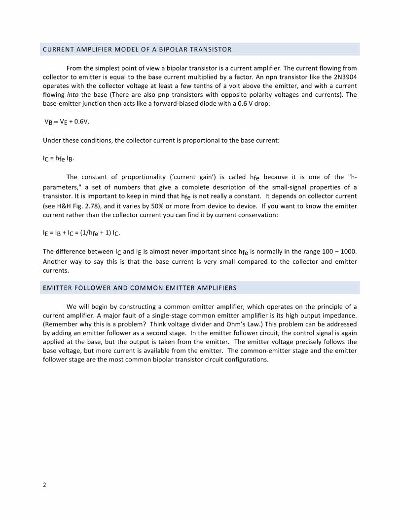
EMITTERFOLLOWERANDCOMMONEMITTERAMPLIFIERS Wewillbeginbyconstructingacommonemitteramplifier,whichoperateson theprincipleofacurrentamplifier.Amajorfaultofasingle-stagecommonemitteramplifier is itshighoutputimpedance.(Rememberwhythisisaproblem?ThinkvoltagedividerandOhm’sLaw.)Thisproblemcanbeaddressedbyaddinganemitterfollowerasasecondstage.Intheemitterfollowercircuit,thecontrolsignalisagainappliedat thebase,but theoutput is takenfromtheemitter. Theemittervoltageprecisely followsthebasevoltage,butmorecurrentisavailablefromtheemitter.Thecommon-emitterstageandtheemitterfollowerstagearethemostcommonbipolartransistorcircuitconfigurations.
3
Figure2Twobasictransistoramplifiers.(a)EmitterFollowerand(b)Commonemitter.
Intheemitter-followerstageofFigure2a,theoutput(emitter)voltageisalways0.6V(onediodedrop)belowtheinput(base)voltage.AsmallsignalofamplitudeδVattheinputwillthereforegiveasignalδVattheoutput,i.e.theoutputjust“follows”theinput.Aswewillseelater,theadvantageofthiscircuitthatithashighinputimpedanceandlowoutputimpedance. Inthecommon-emitterstageofFigure2b,asmallsignalofamplitudeδVattheinputwillagaingiveasignalδVattheemitter.ThiswillcauseavaryingcurrentofamplitudeδV/REtoflowfromtheemittertoground,andhencealsothroughRC.ThiscurrentgeneratesaVoutof–RC(δV/RE).Thusthecommonemitterstagehasasmall-signalvoltagegainof:
𝐺 = −𝑅!𝑅!
Note: thisGain isaboutthechange involtage,which isabitdifferentthantheearlier“Gains”youwereworkingwith.
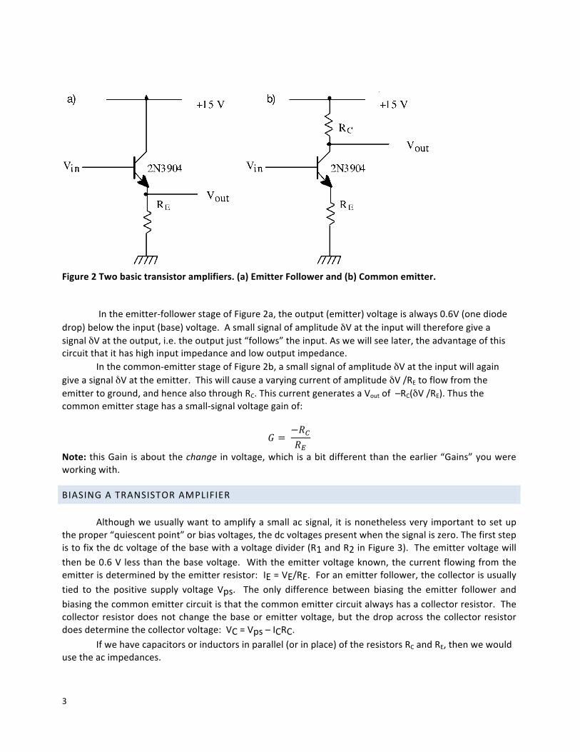
BIASINGATRANSISTORAMPLIFIER Althoughweusuallywanttoamplifyasmallacsignal, it isnonethelessvery importanttosetuptheproper“quiescentpoint”orbiasvoltages,thedcvoltagespresentwhenthesignaliszero.Thefirststepistofixthedcvoltageofthebasewithavoltagedivider(R1andR2inFigure3).Theemittervoltagewillthenbe0.6V lessthanthebasevoltage. Withtheemittervoltageknown,thecurrentflowingfromtheemitterisdeterminedbytheemitterresistor:IE=VE/RE.Foranemitterfollower,thecollectorisusuallytied to the positive supply voltage Vps. The only difference between biasing the emitter follower andbiasingthecommonemittercircuitisthatthecommonemittercircuitalwayshasacollectorresistor.Thecollectorresistordoesnotchangethebaseoremittervoltage,butthedropacrossthecollectorresistordoesdeterminethecollectorvoltage:VC=Vps–ICRC. Ifwehavecapacitorsorinductorsinparallel(orinplace)oftheresistorsRCandRE,thenwewouldusetheacimpedances.
4
Figure3.Common-emitteramplifierwithbiasingresistorsinplace.
OUTPUTRANGEOFTHECOMMONEMITTERAMPLIFER(CLIPPINGVOLTAGES) Evenwithproperbiasingofthetransistor,theoutputvoltagehasarangethatislessthan0−15V.Let’s determine themaximum andminimum output voltages. Since Vout = 15 V – ICRC, themaximumvoltagewilloccurwhenIC=0andtheminimumvoltagewhenICisamaximum.Maximumvoltage:Thisoccurswhenthetransistoristurnedoffandnocurrentisflowing.AsthereisnocurrentflowingthroughRC,thereisnovoltagedropacrossit.ThusVout=Vmax=15V.MinimumVoltage:Thisoccurswhenthetransistorisfullyon.Themaximumcurrentisflowingandthereisverylittlevoltagedropacrossthetransistor.Thevoltageis: Vout=Vmin=15V–RCIC(max)IC(max)canbefoundbyconsideringthevoltagedropfromthepowersupplytogroundwhenthereisnovoltagedropacrossthetransistor:15V–RCIC−REIE=0.Thissimplemodeldoesnotincludethe~0.1Vdropacrossthetransistoritselfevenwhenitisfullyon.
INPUTANDOUTPUTIMPEDANCES The input impedance is the same for both emitter followers and common emitter stages. Theinputimpedancelookingintothebaseis
𝑟!" = 𝑅! ℎ!" InthisexpressionREiswhateverimpedanceisconnectedtotheemitter.Foracommonemitterstage,RE
wouldusually justbetheemitterresistor,butforanemitterfollowerREmightbetheemitterresistor inparallelwiththeinputimpedanceofthenextstage.Ifyouwanttheinputimpedanceofthewholecircuit,rather than just that looking intothebase,youwillhavetoconsiderrin inparallelwiththebasebiasresistors.
5
Theoutputimpedanceofacommonemitterstage(Fig.2b)aloneisjustequaltothecollectorresistorRC.
𝑟!"# = 𝑅! (commonemitterstage)Theoutputimpedancelookingintotheemitterofanemitterfollower(e.g.Fig.2a)isgivenby
𝑟!"# =!!
!!"!!(emitterfollowerstage)
RB stands for whatever impedance is connected to the base. Usually this impedance is in parallel with whateverimpedanceisconnectedtotheemitter(RE).
EBERS-MOLLMODELOFABIPOLARTRANSISTOR Aslightlymorecompletemodelofthebipolartransistorisrequiredtounderstandwhathappenswhentheemitterresistorisverysmall.Insteadofusingthecurrentamplifiermodel,onecantaketheviewthatthecollectorcurrentICiscontrolledbythebase-emittervoltageVBE.Forourpurposes,theEbers-Mollmodelmodifiesourcurrentamplifiermodelofthetransistorinonlyoneimportantway.Forsmallvariationsaboutthequiescentpoint,thetransistornowactsasifithasasmallinternalresistor,re,inserieswiththeemitter.Themagnitudeoftheintrinsicemitterresistance,re,dependsonthecollectorcurrentIC.
𝑟! = 25Ω 1 𝑚𝐴𝐼!
Thepresenceoftheintrinsicemitterresistance,re,modifiestheaboveequationsasfollows.
𝑟!" = (𝑅! + 𝑟!)ℎ!"
𝑟!"# =!!
!!"!!+ 𝑟! (emitterfollowerstage)
Themostimportantoftheseresultsisthemodifiedgain:
𝐺 = −𝑅!𝑅! + 𝑟!
whichshowsthatthecommonemittergainisnotinfinitewhentheexternalemitterresistorgoestozero.
USEFULREADINGS1. Diefenderfer&Holton8.1–8.42. Adatasheetforthe2N3904transistorispostedonourcoursewebsite.3. HorowitzandHill,Chapter2. Themost importantsectionsare2.01–2.03,2.05, thefirstpageof
2.06,2.07,2.09–2.12,andthepartof2.13onpage84and85.HavealookatTable2.1andFigure2.78forasummaryofthespecificationsofsomerealdevices.
LABPREPACTIVITIES
AnswerthefollowingquestionsusingMathematicaorbyhandinyourlabbook.Bringanelectroniccopyofyournotebooktolab,preferablyonyourownlaptop.
6
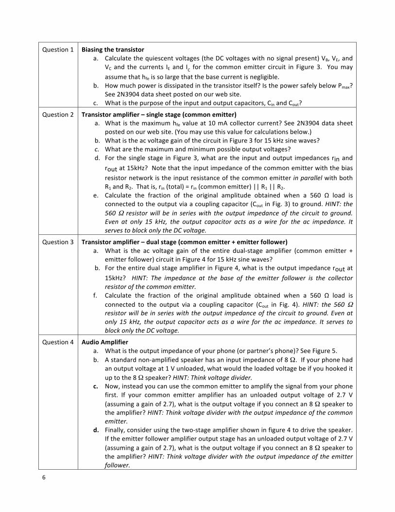
Question1
Biasingthetransistora. Calculatethequiescentvoltages(theDCvoltageswithnosignalpresent)VB,VE,and
VC and the currents IE and IC for the commonemitter circuit in Figure 3. Youmayassumethathfeissolargethatthebasecurrentisnegligible.
b. Howmuchpowerisdissipatedinthetransistoritself?IsthepowersafelybelowPmax?See2N3904datasheetpostedonourwebsite.
c. Whatisthepurposeoftheinputandoutputcapacitors,CinandCout?
Question2
Transistoramplifier–singlestage(commonemitter)a. What is themaximumhfevalueat10mAcollectorcurrent?See2N3904datasheet
postedonourwebsite.(Youmayusethisvalueforcalculationsbelow.)b. WhatistheacvoltagegainofthecircuitinFigure3for15kHzsinewaves?c. Whatarethemaximumandminimumpossibleoutputvoltages?d. For thesingle stage inFigure3,whatare the inputandoutput impedances rinand
routat15kHz?NotethattheinputimpedanceofthecommonemitterwiththebiasresistornetworkistheinputresistanceofthecommonemitterinparallelwithbothR1andR2.Thatis,rin(total)=rin(commonemitter)||R1||R2.
e. Calculate the fraction of the original amplitude obtained when a 560 Ω load isconnectedtotheoutputviaacouplingcapacitor(Cout inFig.3)toground.HINT:the560Ω resistorwill be in serieswith theoutput impedanceof the circuit to ground.Even at only 15 kHz, the output capacitor acts as a wire for the ac impedance. ItservestoblockonlytheDCvoltage.
Question3
Transistoramplifier–dualstage(commonemitter+emitterfollower)a. What is the ac voltage gain of the entire dual-stage amplifier (common emitter +
emitterfollower)circuitinFigure4for15kHzsinewaves?b. FortheentiredualstageamplifierinFigure4,whatistheoutputimpedanceroutat
15kHz? HINT: The impedance at the base of the emitter follower is the collectorresistorofthecommonemitter.
f. Calculate the fraction of the original amplitude obtained when a 560 Ω load isconnected to the output via a coupling capacitor (Cout in Fig. 4).HINT: the 560Ωresistorwillbe inserieswiththeoutput impedanceofthecircuit toground.Evenatonly 15 kHz, the output capacitor acts as awire for the ac impedance. It serves toblockonlytheDCvoltage.
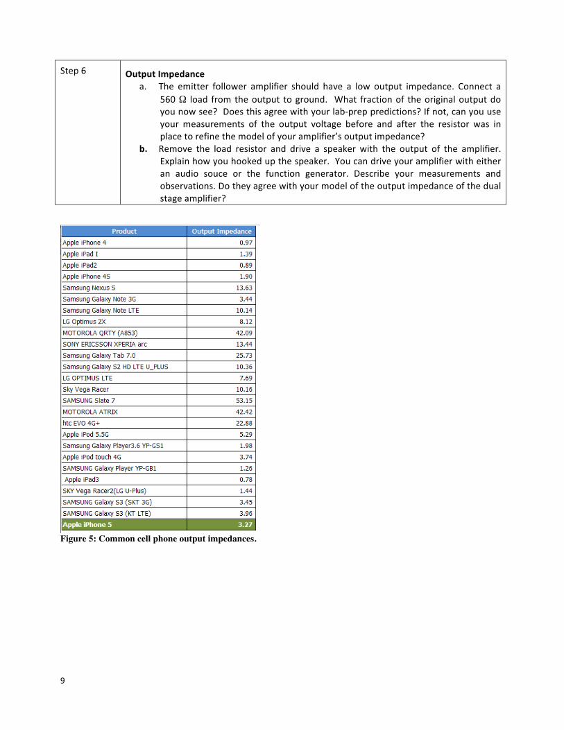
Question4 AudioAmplifiera. Whatistheoutputimpedanceofyourphone(orpartner’sphone)?SeeFigure5.b. Astandardnon-amplifiedspeakerhasaninputimpedanceof8Ω.Ifyourphonehad
anoutputvoltageat1Vunloaded,whatwouldtheloadedvoltagebeifyouhookedituptothe8Ωspeaker?HINT:Thinkvoltagedivider.
c. Now,insteadyoucanusethecommonemittertoamplifythesignalfromyourphonefirst. If your common emitter amplifier has an unloaded output voltage of 2.7 V(assumingagainof2.7),whatistheoutputvoltageifyouconnectan8Ωspeakertotheamplifier?HINT:Thinkvoltagedividerwiththeoutputimpedanceofthecommonemitter.
d. Finally,considerusingthetwo-stageamplifiershowninfigure4todrivethespeaker.Iftheemitterfolloweramplifieroutputstagehasanunloadedoutputvoltageof2.7V(assumingagainof2.7),whatistheoutputvoltageifyouconnectan8Ωspeakertotheamplifier?HINT:Thinkvoltagedividerwiththeoutput impedanceoftheemitterfollower.
7
Question5 Labactivitiesa. Readthroughallofthelabstepsandidentifythestep(orsub-step)thatyouthinkwill
bethemostchallenging.b. Listatleastonequestionyouhaveaboutthelabactivity.
COMMOMEMITTERAMPLIFIER
Step1
QuiescentState a. BuildthecommonemitteramplifiershowninFigure3(withoutthecapacitorsCin
andCout)andcheckthatthecorrectdclevels(quiescentvoltages)areestablished.Measure the resistorsbeforeputting them in thecircuit, and if theydiffer fromthevaluesusedinyourcalculations,recalculatethepredictedquiescentvoltages.Drawthecircuitschematic inyour labbookand labelall components.Whatarethe dc levels VB (at the transistor base), VE (at the emitter) and VC (at thecollector)?Dotheyagreewithyourpredictions?
Step2 LowfrequencyACGaina. ConvertthepreviouscircuittoanACamplifierbyaddingthecouplingcapacitors
CinandCout.Makesuretogetthepolaritycorrect(forCout,considergroundontheright).Thecapacitorswilltransmitacsignalsbutblockdcsignals.Thisallowsyoutoconnectsignalswithoutdisturbingthequiescentconditions.
b. When you switch on the power, you may see high frequency spontaneousoscillations. These must be suppressed before you can proceed. An additionalbypasscapacitor(~100nF)between+15Vandgroundclosetothetransistormayhelp.Also,reducingthelengthofyourcircuitwirescanhelp.
c. Assembleatestset-uptoobservethe inputandoutputoftheamplifierwith15kHzsinewaves,usingthe10xscopeprobefortheoutput.HINT:Youmayneedtoadda220kΩresistortogroundafterCouttokeepthedclevelatthescopeinputnear ground as the large output capacitor can slowly charge up. Youmay alsowanttoputthescopeonaccouplingwhenyouprobepointswithlargedcoffsetsbutswitchitbacktoDCifyouwanttomeasurequiescentvoltages.Varytheinputamplitude todetermine theoutputamplitudeatwhich clippingbegins. Youwillwant to stay below half of this clipping voltage to assure the amplifier is notdistortingtheoutputwaveform.
d. Measurethegainoftheamplifierfor15kHzsinewaves.Doesyourmeasurementagreewithyourprediction?
Step3 OutputImpedancea. The common emitter amplifier often has a large output impedance. Connect a
560Ω load fromtheoutput toground. What fractionof theoriginaloutputdoyounowsee?Doesthisagreewithyourlab-preppredictions?Ifnot,canyouuseyourmeasurements of the output voltage before and after the resistor was inplacetorefinethemodelofyouramplifier’soutputimpedance?
b. Remove the load resistor and drive a speakerwith the output of the amplifier.Explainhowyouhookedupthespeaker.Firstdrivethecircuitwiththefunctiongenerator. Describe your measurements and observations. Do they agree withyour model of the output impedance of the common emitter amplifier?HINT:
8
Consider themaximumandminimumoutput voltagespossible you calculated intheprelab.
c. Now drive the circuit with an audio source. Describe your measurements andobservations.
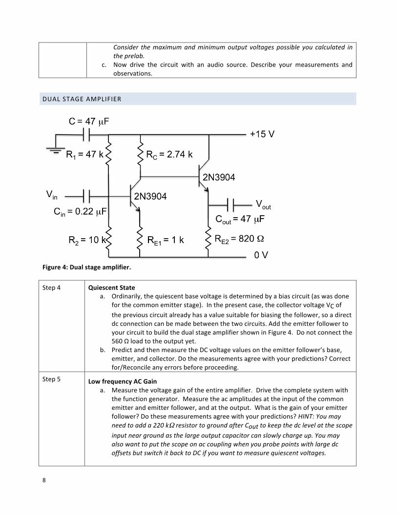
DUALSTAGEAMPLIFIER
Figure4:Dualstageamplifier.
Step4
QuiescentState a. Ordinarily,thequiescentbasevoltageisdeterminedbyabiascircuit(aswasdone
forthecommonemitterstage).Inthepresentcase,thecollectorvoltageVCofthepreviouscircuitalreadyhasavaluesuitableforbiasingthefollower,soadirectdcconnectioncanbemadebetweenthetwocircuits.AddtheemitterfollowertoyourcircuittobuildthedualstageamplifiershowninFigure4.Donotconnectthe560Ωloadtotheoutputyet.
b. PredictandthenmeasuretheDCvoltagevaluesontheemitterfollower’sbase,emitter,andcollector.Dothemeasurementsagreewithyourpredictions?Correctfor/Reconcileanyerrorsbeforeproceeding.
Step5 LowfrequencyACGaina. Measurethevoltagegainoftheentireamplifier.Drivethecompletesystemwith
thefunctiongenerator.Measuretheacamplitudesattheinputofthecommonemitterandemitterfollower,andattheoutput.Whatisthegainofyouremitterfollower?Dothesemeasurementsagreewithyourpredictions?HINT:Youmayneedtoadda220kΩresistortogroundafterCouttokeepthedclevelatthescopeinputneargroundasthelargeoutputcapacitorcanslowlychargeup.YoumayalsowanttoputthescopeonaccouplingwhenyouprobepointswithlargedcoffsetsbutswitchitbacktoDCifyouwanttomeasurequiescentvoltages.
9
Step6 OutputImpedancea. The emitter follower amplifier should have a low output impedance. Connect a
560Ω load fromtheoutput toground. What fractionof theoriginaloutputdoyounowsee?Doesthisagreewithyourlab-preppredictions?Ifnot,canyouuseyour measurements of the output voltage before and after the resistor was inplacetorefinethemodelofyouramplifier’soutputimpedance?
b. Remove the load resistor and drive a speaker with the output of the amplifier.Explainhowyouhookedupthespeaker.Youcandriveyouramplifierwitheitheran audio souce or the function generator. Describe your measurements andobservations.Dotheyagreewithyourmodeloftheoutputimpedanceofthedualstageamplifier?
Figure 5: Common cell phone output impedances.