
BCM5221 Data Sheet - pudn.comread.pudn.com/downloads746/doc/2975733/5221-DS23-R.pdf · • Unique...
107
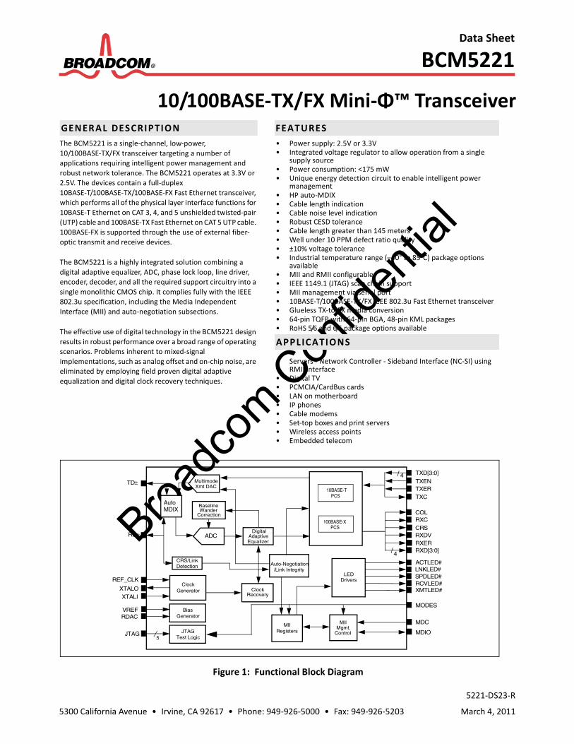
Broadcom Confidential Data Sheet BCM5221 5221-DS23-R 5300 California Avenue • Irvine, CA 92617 • Phone: 949-926-5000 • Fax: 949-926-5203 March 4, 2011 10/100BASE-TX/FX Mini-Φ™ Transceiver Figure 1: Functional Block Diagram GENERAL DESCRIPTION FEATURES The BCM5221 is a single-channel, low-power, 10/100BASE-TX/FX transceiver targeting a number of applications requiring intelligent power management and robust network tolerance. The BCM5221 operates at 3.3V or 2.5V. The devices contain a full-duplex 10BASE-T/100BASE-TX/100BASE-FX Fast Ethernet transceiver, which performs all of the physical layer interface functions for 10BASE-T Ethernet on CAT 3, 4, and 5 unshielded twisted-pair (UTP) cable and 100BASE-TX Fast Ethernet on CAT 5 UTP cable. 100BASE-FX is supported through the use of external fiber- optic transmit and receive devices. The BCM5221 is a highly integrated solution combining a digital adaptive equalizer, ADC, phase lock loop, line driver, encoder, decoder, and all the required support circuitry into a single monolithic CMOS chip. It complies fully with the IEEE 802.3u specification, including the Media Independent Interface (MII) and auto-negotiation subsections. The effective use of digital technology in the BCM5221 design results in robust performance over a broad range of operating scenarios. Problems inherent to mixed-signal implementations, such as analog offset and on-chip noise, are eliminated by employing field proven digital adaptive equalization and digital clock recovery techniques. • Power supply: 2.5V or 3.3V • Integrated voltage regulator to allow operation from a single supply source • Power consumption: <175 mW • Unique energy detection circuit to enable intelligent power management • HP auto-MDIX • Cable length indication • Cable noise level indication • Robust CESD tolerance • Cable length greater than 145 meters • Well under 10 PPM defect ratio quality • ±10% voltage tolerance • Industrial temperature range (–40° to 85°C) package options available • MII and RMII configurable • IEEE 1149.1 (JTAG) scan chain support • MII management via serial port • 10BASE-T/100BASE-TX/FX IEEE 802.3u Fast Ethernet transceiver • Glueless TX-to-FX media conversion • 64-pin TQFP with 64-pin BGA, 48-pin KML packages • RoHS 5/6 and 6/6 package options available APPLICATIONS • Servers - Network Controller - Sideband Interface (NC-SI) using RMII interface • Digital TV • PCMCIA/CardBus cards • LAN on motherboard • IP phones • Cable modems • Set-top boxes and print servers • Wireless access points • Embedded telecom MII MII Equalizer Auto-Negotiation LED Clock Bias Registers Mgmt. Control Correction /Link Integrity Generator Generator Wander Baseline TXD[3:0] TXEN TXER TXC COL RXC CRS RXDV RXER RXD[3:0] LNKLED# MDC MDIO MODES TD± RD± XTALO Recovery Xmt DAC ADC SPDLED# RCVLED# XMTLED# Multimode Digital Adaptive 10BASE-T PCS 100BASE-X PCS Drivers Clock XTALI VREF RDAC ACTLED# REF_CLK Detection CRS/Link 4 4 JTAG Test Logic JTAG 5 Auto MDIX
Transcript of BCM5221 Data Sheet - pudn.comread.pudn.com/downloads746/doc/2975733/5221-DS23-R.pdf · • Unique...
Broadc
om C
onfid
entia
l
Data Sheet
BCM5221
5221-DS23-R
5300 California Avenue • Irvine, CA 92617 • Phone: 949-926-5000 • Fax: 949-926-5203 March 4, 2011
10/100BASE-TX/FX Mini-Φ™ Transceiver
Figure 1: Functional Block Diagram
GENERAL DESCRIPTION FEATURESThe BCM5221 is a single-channel, low-power, 10/100BASE-TX/FX transceiver targeting a number of applications requiring intelligent power management and robust network tolerance. The BCM5221 operates at 3.3V or 2.5V. The devices contain a full-duplex 10BASE-T/100BASE-TX/100BASE-FX Fast Ethernet transceiver, which performs all of the physical layer interface functions for 10BASE-T Ethernet on CAT 3, 4, and 5 unshielded twisted-pair (UTP) cable and 100BASE-TX Fast Ethernet on CAT 5 UTP cable. 100BASE-FX is supported through the use of external fiber-optic transmit and receive devices.
The BCM5221 is a highly integrated solution combining a digital adaptive equalizer, ADC, phase lock loop, line driver, encoder, decoder, and all the required support circuitry into a single monolithic CMOS chip. It complies fully with the IEEE 802.3u specification, including the Media Independent Interface (MII) and auto-negotiation subsections.
The effective use of digital technology in the BCM5221 design results in robust performance over a broad range of operating scenarios. Problems inherent to mixed-signal implementations, such as analog offset and on-chip noise, are eliminated by employing field proven digital adaptive equalization and digital clock recovery techniques.
• Power supply: 2.5V or 3.3V• Integrated voltage regulator to allow operation from a single
supply source• Power consumption: <175 mW• Unique energy detection circuit to enable intelligent power
management• HP auto-MDIX• Cable length indication• Cable noise level indication• Robust CESD tolerance• Cable length greater than 145 meters• Well under 10 PPM defect ratio quality• ±10% voltage tolerance• Industrial temperature range (–40° to 85°C) package options
available• MII and RMII configurable• IEEE 1149.1 (JTAG) scan chain support• MII management via serial port• 10BASE-T/100BASE-TX/FX IEEE 802.3u Fast Ethernet transceiver• Glueless TX-to-FX media conversion• 64-pin TQFP with 64-pin BGA, 48-pin KML packages• RoHS 5/6 and 6/6 package options available
APPLICATIONS
• Servers - Network Controller - Sideband Interface (NC-SI) using RMII interface
• Digital TV• PCMCIA/CardBus cards • LAN on motherboard• IP phones • Cable modems • Set-top boxes and print servers• Wireless access points• Embedded telecom
MII MII
Equalizer
Auto-Negotiation
LED
Clock
Bias
RegistersMgmt.
Control
Correction
/Link Integrity
Generator
Generator
WanderBaseline
TXD[3:0]
TXENTXERTXC
COLRXC CRS RXDV RXER RXD[3:0]
LNKLED#
MDC
MDIO
MODES
TD±
RD±
XTALORecovery
Xmt DAC
ADC
SPDLED# RCVLED# XMTLED#
Multimode
DigitalAdaptive
10BASE-TPCS
100BASE-XPCS
DriversClock
XTALI
VREFRDAC
ACTLED#
REF_CLK
DetectionCRS/Link
4
4
JTAGTest Logic
JTAG5
AutoMDIX
Broadc
om C
onfid
entia
l
Revision HistoryBCM5221 Data Sheet
BROADCOM March 4, 2011 • 5221-DS23-R Page 2
®
Revision History
Revision Date Change Description
5221-DS23-R 03/04/11 Updated:• Table 56: “Recommended Operating Conditions,” on page 97• Table 57: “Electrical Characteristics,” on page 97• Table 62: “Main Differences between Standard and RoHS-Compliant
Packages,” on page 101• Section 11: “Ordering Information,” on page 106
5221-DS22-D1 11/01/10 Updated:• Update vih and vil at OVDD=2.5V
5221-DS21-R 11/02/09 Updated:• Removed BCM5221A4IML references
5221-DS20-R 07/08/09 Updated:• Table 62, ”Main Differences between Standard and RoHS-Compliant
Packages,” on page 76 (part number BCM5221A4KML removed).• Section 11 ”Ordering Information” on page 80 (part number
BCM5221A4KML removed).
5221-DS19-R 06/09/09 Updated:• Figure 6, ”MII Transmit Start of Packet Timing (100BASE-TX),” on page 60• Figure 7, ”MII Transmit End of Packet Timing (100BASE-TX),” on page 60• Table 41, ”MII 100BASE-X Receive Timing,” on page 61
5221-DS18-R 01/09/09 Updated:• H5, G5 in Table 3, ”Pin Descriptions,” on page 7
5221-DS17-R 10/16/08 Updated:• Table 62 on page 76• Section 11: “Ordering Information” on page 80
5221-DS16-R 08/18/08 Added:• Notes in Table 3 on page 7 stating that JTAG function is not supported in
the KML package.
5221-DS15-R 06/25/08 Updated:• Table 4,”10BASE-T Serial Mode (7-Wire) Signals,” on page 17.• Table 39,”Reset Timing,” on page 62.
5221-DS14-R 11/16/07 Updated:• Figure 4,”BCM5221KML Pin Diagram,” on page 14: Changed pin 4 from
unconnected to GND.
5221-DS13-R 11/09/07 Updated:• Table 3,”Pin Descriptions,” on page 7: Changed pin 4 from unconnected to
GND.
5221-DS12-R 08/23/07 Updated:• Table 52,”RMII Receive Timing,” on page 72.
5221-DS11-R 07/05/07 Initial release.

Broadc
om C
onfid
entia
l
Broadcom®, the pulse logo, Connecting everything®, the Connecting everything logo, and and Mini-Φ™ are among the trademarks of Broadcom Corporation and/or its affiliates in the United States, certain other
countries and/or the EU. Any other trademarks or trade names mentioned are the property of their respective owners.
This data sheet (including, without limitation, the Broadcom component(s) identified herein) is not designed, intended, or certified for use in any military, nuclear, medical, mass transportation, aviation, navigations,
pollution control, hazardous substances management, or other high-risk application. BROADCOM PROVIDES THIS DATA SHEET “AS-IS,” WITHOUT WARRANTY OF ANY KIND. BROADCOM DISCLAIMS ALL WARRANTIES,
EXPRESSED AND IMPLIED, INCLUDING, WITHOUT LIMITATION, THE IMPLIED WARRANTIES OF MERCHANTABILITY, FITNESS FOR A PARTICULAR PURPOSE, AND NON-INFRINGEMENT.
Broadcom Corporation5300 California Avenue
Irvine, CA 92617
© 2011 by Broadcom CorporationAll rights reserved
Printed in the U.S.A.
Broadc
om C
onfid
entia
l
Table of Contents BCM5221 Data Sheet
BROADCOM March 4, 2011 • 5221-DS23-R Page 4
®
Table of ContentsAbout This Document...................................................................................................................................14
Purpose and Audience ...........................................................................................................................14
Acronyms and Abbreviations.................................................................................................................14
Document Conventions .........................................................................................................................14
References .............................................................................................................................................15
Technical Support .........................................................................................................................................15
Section 1: Functional Description .................................................................................... 16
Overview.......................................................................................................................................................16
Encoder/Decoder .........................................................................................................................................16
Link Monitor .................................................................................................................................................17
Carrier Sense.................................................................................................................................................17
Collision Detection .......................................................................................................................................17
Auto-negotiation ..........................................................................................................................................18
Digital Adaptive Equalizer ............................................................................................................................18
ADC ...............................................................................................................................................................18
Digital Clock Recovery/Generator ...............................................................................................................18
Baseline Wander Correction ........................................................................................................................19
Multimode Transmit DAC.............................................................................................................................19
Stream Cipher ...............................................................................................................................................19
Far-End Fault.................................................................................................................................................20
RMII Interface ...............................................................................................................................................20
MII Management ..........................................................................................................................................21
Section 2: Hardware Signal Definitions............................................................................ 23
Section 3: Pinout Diagram ............................................................................................... 30
Section 4: Operational Description .................................................................................. 33
Reset .............................................................................................................................................................33
Isolate Mode.................................................................................................................................................33
Super Isolate Mode ......................................................................................................................................33
Loopback Mode ............................................................................................................................................34
Full-Duplex Mode .........................................................................................................................................34
100BASE-FX Mode ........................................................................................................................................34
10BASE-T Mode ............................................................................................................................................35
10BASE-T Serial Mode ..................................................................................................................................35
Broadc
om C
onfid
entia
l
Table of Contents BCM5221 Data Sheet
BROADCOM March 4, 2011 • 5221-DS23-R Page 5
®
Special LED Modes........................................................................................................................................35
Traffic Meter Mode................................................................................................................................35
Force LEDs On ........................................................................................................................................36
Disable LEDs...........................................................................................................................................36
Interrupt Mode .............................................................................................................................................36
Energy Detection ..........................................................................................................................................36
Power-saving Modes ....................................................................................................................................37
Auto Power-down Mode..............................................................................................................................37
HP Auto-MDIX ..............................................................................................................................................38
Section 5: Register Summary........................................................................................... 39
MII Management Interface: Register Programming ...................................................................................39
Preamble (PRE) ......................................................................................................................................39
Start of Frame (ST) .................................................................................................................................39
Operation Code (OP)..............................................................................................................................39
PHY Address (PHYAD) ............................................................................................................................39
Register Address (REGAD)......................................................................................................................40
Turnaround (TA).....................................................................................................................................40
Data........................................................................................................................................................40
Idle .........................................................................................................................................................40
MII Register Map Summary .........................................................................................................................41
MII Control Register .....................................................................................................................................45
Reset ......................................................................................................................................................45
Loopback................................................................................................................................................45
Forced Speed Selection..........................................................................................................................46
Auto-Negotiation Enable .......................................................................................................................46
Power Down ..........................................................................................................................................46
Isolate ....................................................................................................................................................46
Restart Auto-Negotiation.......................................................................................................................46
Duplex Mode..........................................................................................................................................46
Collision Test..........................................................................................................................................47
Reserved Bits .........................................................................................................................................47
MII Status Register .......................................................................................................................................48
100BASE-T4 Capability ...........................................................................................................................48
100BASE-X Full-Duplex Capability..........................................................................................................48
100BASE-X Half-Duplex Capability .........................................................................................................48
10BASE-T Full-Duplex Capability ............................................................................................................49
10BASE-T Half-Duplex Capability ...........................................................................................................49
Broadc
om C
onfid
entia
l
Table of Contents BCM5221 Data Sheet
BROADCOM March 4, 2011 • 5221-DS23-R Page 6
®
Reserved Bits .........................................................................................................................................49
Preamble Suppression ...........................................................................................................................49
Auto-Negotiation Complete...................................................................................................................49
Remote Fault..........................................................................................................................................49
Auto-Negotiation Capability ..................................................................................................................49
Link Status..............................................................................................................................................49
Jabber Detect.........................................................................................................................................50
Extended Capability ...............................................................................................................................50
PHY Identifier Registers................................................................................................................................50
Auto-Negotiation Advertisement Register ..................................................................................................50
Next Page...............................................................................................................................................51
Reserved Bits .........................................................................................................................................51
Remote Fault..........................................................................................................................................51
Reserved Technologies Bits ...................................................................................................................51
Pause......................................................................................................................................................52
Advertisement Bits ................................................................................................................................52
Selector Field .........................................................................................................................................52
Auto-Negotiation Link Partner Ability Register...........................................................................................52
LP Next Page ..........................................................................................................................................53
LP Acknowledge.....................................................................................................................................53
LP Remote Fault .....................................................................................................................................53
Reserved Bits .........................................................................................................................................53
LP Advertise Pause.................................................................................................................................53
LP Advertise Bits ....................................................................................................................................53
LP Selector Field.....................................................................................................................................53
Auto-Negotiation Expansion Register..........................................................................................................53
Reserved Bits .........................................................................................................................................54
Parallel Detection Fault..........................................................................................................................54
Link Partner Next Page Able ..................................................................................................................54
Next Page Able.......................................................................................................................................54
Page Received........................................................................................................................................54
Link Partner Auto-Negotiation Able.......................................................................................................55
Auto-Negotiation Next Page Register..........................................................................................................55
Next Page...............................................................................................................................................55
Message Page ........................................................................................................................................55
Acknowledge 2.......................................................................................................................................55
Broadc
om C
onfid
entia
l
Table of Contents BCM5221 Data Sheet
BROADCOM March 4, 2011 • 5221-DS23-R Page 7
®
Toggle.....................................................................................................................................................55
Message Code Field ...............................................................................................................................56
Unformatted Code Field ........................................................................................................................56
Auto-Negotiation Link Partner Next Page Transmit Register .....................................................................57
Next Page...............................................................................................................................................57
Message Page ........................................................................................................................................57
Acknowledge 2.......................................................................................................................................57
Toggle.....................................................................................................................................................57
Message Code Field ...............................................................................................................................57
Unformatted Code Field ........................................................................................................................58
100BASE-X Auxiliary Control Register..........................................................................................................59
Transmit Disable ....................................................................................................................................59
Bypass 4B5B Encoder/Decoder..............................................................................................................59
Bypass Scrambler/Descrambler .............................................................................................................60
Bypass NRZI Encoder/Decoder ..............................................................................................................60
Bypass Receive Symbol Alignment ........................................................................................................60
Baseline Wander Correction Disable .....................................................................................................60
FEF Enable..............................................................................................................................................60
Extended RMII FIFO Enable....................................................................................................................60
RMII Out-of-Band Enable .......................................................................................................................60
Reserved Bits .........................................................................................................................................60
100BASE-X Auxiliary Status Register............................................................................................................61
RMII Overrun/Underrun Error ...............................................................................................................61
FX Mode.................................................................................................................................................61
Locked....................................................................................................................................................62
Current 100BASE-X Link Status ..............................................................................................................62
Remote Fault..........................................................................................................................................62
False Carrier Detected ...........................................................................................................................62
Bad ESD Detected ..................................................................................................................................62
Receive Error Detected ..........................................................................................................................62
Transmit Error Detected ........................................................................................................................62
Lock Error Detected ...............................................................................................................................62
MLT3 Code Error Detected ....................................................................................................................62
100BASE-X Receive Error Counter................................................................................................................63
Receive Error Counter [15:0] .................................................................................................................63
100BASE-X False Carrier Sense Counter ......................................................................................................63
RMII Overrun/Underrun Counter [7:0]..................................................................................................63
Broadc
om C
onfid
entia
l
Table of Contents BCM5221 Data Sheet
BROADCOM March 4, 2011 • 5221-DS23-R Page 8
®
False Carrier Sense Counter [7:0] ..........................................................................................................63
100BASE-X Disconnect Counter ...................................................................................................................64
RMII Fast RXD.........................................................................................................................................64
RMII Slow RXD........................................................................................................................................64
Ptest Register................................................................................................................................................64
Auxiliary Control/Status Register ................................................................................................................65
Jabber Disable........................................................................................................................................65
Link Force...............................................................................................................................................65
HSQ and LSQ ..........................................................................................................................................66
Edge Rate ...............................................................................................................................................66
Auto-Negotiation Indication ..................................................................................................................66
Force 100/10 Indication.........................................................................................................................66
Speed Indication ....................................................................................................................................66
Full-Duplex Indication ............................................................................................................................66
Auxiliary Status Summary Register..............................................................................................................67
Interrupt Register .........................................................................................................................................68
FDX LED Enable ......................................................................................................................................68
Interrupt Enable.....................................................................................................................................68
FDX Mask ...............................................................................................................................................68
SPD Mask ...............................................................................................................................................69
Link Mask ...............................................................................................................................................69
Interrupt Mask .......................................................................................................................................69
FDX Change............................................................................................................................................69
SPD Change............................................................................................................................................69
Link Change............................................................................................................................................69
Interrupt Status......................................................................................................................................69
Auxiliary Mode 2 Register ............................................................................................................................70
10BT Dribble Bit Correct ........................................................................................................................70
Token Ring Mode...................................................................................................................................70
HSTR FIFO Mode ....................................................................................................................................70
Block 10BT Echo Mode ..........................................................................................................................70
Traffic Meter LED Mode.........................................................................................................................71
Activity LED Force On.............................................................................................................................71
Activity/Link LED Mode..........................................................................................................................71
Qualified Parallel Detect Mode..............................................................................................................71
10BASE-T Auxiliary Error and General Status Register................................................................................71
Broadc
om C
onfid
entia
l
Table of Contents BCM5221 Data Sheet
BROADCOM March 4, 2011 • 5221-DS23-R Page 9
®
MDIX Status ...........................................................................................................................................72
MDIX Manual Swap................................................................................................................................72
HP Auto-MDIX Disable ...........................................................................................................................72
Manchester Code Error..........................................................................................................................72
End of Frame Error.................................................................................................................................73
Auto-negotiation Indication...................................................................................................................73
Force 100/10 Indication.........................................................................................................................73
Speed Indication ....................................................................................................................................73
Full-Duplex Indication ............................................................................................................................73
Auxiliary Mode Register ............................................................................................................................... 73
Activity LED Disable................................................................................................................................74
Link LED Disable .....................................................................................................................................74
Block TXEN Mode...................................................................................................................................74
Auxiliary Multiple PHY Register ...................................................................................................................74
HCD Bits .................................................................................................................................................75
Restart Auto-negotiation .......................................................................................................................75
Auto-negotiation Complete ...................................................................................................................75
Acknowledge Complete .........................................................................................................................75
Acknowledge Detected..........................................................................................................................76
Ability Detect .........................................................................................................................................76
Super Isolate ..........................................................................................................................................76
10BASE-T Serial Mode............................................................................................................................76
Broadcom Test Register ............................................................................................................................... 76
Block RXDV.............................................................................................................................................77
Shadow Register Enable.........................................................................................................................77
Auxiliary Mode 4 Register (Shadow Register) .............................................................................................77
Force LED [1:0].......................................................................................................................................77
Enable Clock During Low Power ............................................................................................................77
Force IDDQ Mode ..................................................................................................................................78
Auxiliary Status 2 Register (Shadow Register).............................................................................................78
MLT3 Detected ......................................................................................................................................78
Cable Length 100X [2:0].........................................................................................................................78
ADC Peak Amplitude [5:0]......................................................................................................................79
APD Enable.............................................................................................................................................79
APD Sleep TImer ....................................................................................................................................79
APD Wake-up TImer [3:0] ......................................................................................................................79
Auxiliary Status 3 Register (Shadow Register).............................................................................................80
Broadc
om C
onfid
entia
l
Table of Contents BCM5221 Data Sheet
BROADCOM March 4, 2011 • 5221-DS23-R Page 10
®
Noise [7:0]..............................................................................................................................................80
FIFO Consumption [3:0] .........................................................................................................................80
Auxiliary Mode 3 Register (Shadow Register) .............................................................................................81
FIFO Size Select [3:0]..............................................................................................................................81
Auxiliary Status 4 Register (Shadow Register).............................................................................................82
Packet Length Counter [15:0] ................................................................................................................82
Section 6: Timing and AC Characteristics ......................................................................... 83
Section 7: Electrical Characteristics.................................................................................. 97
Section 8: Application Example ....................................................................................... 99
Section 9: Thermal Characteristics................................................................................. 100
Junction Temperature Estimation and PSIJT Versus ThetaJC .....................................................................101
RoHS-Compliant Packaging ........................................................................................................................101
Section 10: Mechanical Information .............................................................................. 103
Section 11: Ordering Information .................................................................................. 106
Broadc
om C
onfid
entia
l
List of Figures BCM5221 Data Sheet
BROADCOM March 4, 2011 • 5221-DS23-R Page 11
®
List of FiguresFigure 1: Functional Block Diagram....................................................................................................................1
Figure 2: BCM5221KPB Ballout Diagram ..........................................................................................................30
Figure 3: BCM5221KPT Pin Diagram.................................................................................................................31
Figure 4: BCM5221KML Pin Diagram ...............................................................................................................32
Figure 5: Clock and Reset Timing......................................................................................................................84
Figure 6: MII Transmit Start of Packet Timing (100BASE-TX) ...........................................................................85
Figure 7: MII Transmit End of Packet Timing (100BASE-TX).............................................................................85
Figure 8: MII Receive Start of Packet Timing (100BASE-TX) .............................................................................87
Figure 9: MII Receive End of Packet Timing (100BASE-TX)...............................................................................87
Figure 10: MII Receive Packet Premature End (100BASE-TX) ..........................................................................88
Figure 11: MII Link Failure or Stream Cipher Error During Receive Packet ......................................................88
Figure 12: MII False Carrier Sense Timing (100BASE-TX) .................................................................................89
Figure 13: MII 10BASE-T Transmit Start of Packet Timing................................................................................90
Figure 14: 10BASE-T Serial Transmit Timing.....................................................................................................91
Figure 15: 10BASE-T Serial Receive Timing ......................................................................................................92
Figure 16: Management Interface Timing........................................................................................................93
Figure 17: Management Interface Timing (with Preamble Suppression On)...................................................94
Figure 18: RMII Transmit Packet Timing...........................................................................................................95
Figure 19: RMII Receive Packet Timing ............................................................................................................96
Figure 20: Power Connections BCM5221 (3.3V) ..............................................................................................99
Figure 21: 64-Pin TQFP 10 mm Package (BCM5221 KPT)...............................................................................103
Figure 22: FBGA 64, 8 mm x 8 mm (BCM5221 KPB) .......................................................................................104
Figure 23: BCM5221KML Package Diagram ...................................................................................................105
Broadc
om C
onfid
entia
l
List of Tables BCM5221 Data Sheet
BROADCOM March 4, 2011 • 5221-DS23-R Page 12
®
List of TablesTable 1: 4B5B Encoding ....................................................................................................................................21
Table 2: Receive Error Encoding.......................................................................................................................22
Table 3: Pin Descriptions ..................................................................................................................................23
Table 4: 10BASE-T Serial Mode (7-Wire) Signals ..............................................................................................35
Table 5: Low-power Modes..............................................................................................................................37
Table 6: MII Management Frame Format ........................................................................................................39
Table 7: MII Register Map Summary ................................................................................................................41
Table 8: MII Shadow Register Map Summary ..................................................................................................44
Table 9: MII Control Register (Address 00000b, 0d, 00h) ................................................................................45
Table 10: MII Status Register (Address 00001B, 01d, 01h) ..............................................................................48
Table 11: PHY Indentifier Registers (Addresses 00010 and 00011b, 02 and 03b, 02 and 03h)........................50
Table 12: Auto-Negotiation Advertisement Register (Address 04d, 04h)........................................................50
Table 13: Auto-Negotiation Link Partner Ability Register (Address 05d, 05h) .................................................52
Table 14: Auto-Negotiation Expansion Register (Address 00110b, 6d, 06h) ...................................................54
Table 15: Next Page Transmit Register (Address 07d, 07h) .............................................................................55
Table 16: Next Page Transmit Register (Address 08d, 08h) .............................................................................57
Table 17: 100BASE-X Auxiliary Control Register (Address 16d, 10h) ...............................................................59
Table 18: 100BASE-X Auxiliary Status Register (Address 17d, 11h) .................................................................61
Table 19: 100BASE-X Receive Error Counter (Address 18d, 12h).....................................................................63
Table 20: 100BASE-X False Carrier Sense Counter (Address 19d, 13h) ............................................................63
Table 21: 100BASE-X Disconnect Counter (Address 20d, 14h).........................................................................64
Table 22: PTEST Register (Address 10111b, 23d, 17h) .....................................................................................64
Table 23: Auxiliary Control/Status Register (Address 24d, 18h) ......................................................................65
Table 24: Auxiliary Status Summary Register (Address 25d, 19h)....................................................................67
Table 25: Interrupt Register (Address 26d, 1Ah)..............................................................................................68
Table 26: Auxiliary Mode 2 Register (Address 27d, 1Bh) .................................................................................70
Table 27: 10BASE-T Auxiliary Error and General Status Register (Address 28d, 1Ch)......................................71
Table 28: Auxiliary Mode Register (Address 29d, 1Dh) ....................................................................................73
Table 29: Auxiliary Multiple PHY Register (Address 30d, 1Eh) .........................................................................74
Table 30: Broadcom Test (Address 31d, 1Fh)...................................................................................................76
Table 31: Auxiliary Mode 4 Register (Shadow Register 26d, 1Ah) ...................................................................77
Table 32: Auxiliary Status 2 Register (Shadow Register 27d, 1Bh)...................................................................78
Table 33: Cable Length .....................................................................................................................................78
Table 34: Auxiliary Status 3 Register (Shadow Register 28d, 1Ch) ...................................................................80
Table 35: Auxiliary Mode 3 Register (Shadow Register 29d, 1Dh) ...................................................................81
Broadc
om C
onfid
entia
l
List of Tables BCM5221 Data Sheet
BROADCOM March 4, 2011 • 5221-DS23-R Page 13
®
Table 36: Current Receive FIFO Size .................................................................................................................81
Table 37: Auxiliary Status 4 Register (Shadow Register 30d, 1Eh) ...................................................................82
Table 38: Clock Timing......................................................................................................................................83
Table 39: Reset Timing .....................................................................................................................................83
Table 40: MII 100BASE-X Transmit Timing .......................................................................................................84
Table 41: MII 100BASE-X Receive Timing .........................................................................................................86
Table 42: MII 10BASE-T Transmit Timing .........................................................................................................89
Table 43: MII 10BASE-T Receive Timing ...........................................................................................................90
Table 44: MII 10BASE-T Collision Timing ..........................................................................................................90
Table 45: 10BASE-T Serial Transmit Timing......................................................................................................91
Table 46: 10BASE-T Serial Receive Timing........................................................................................................92
Table 47: Loopback Timing (MII) ......................................................................................................................92
Table 48: Auto-negotiation Timing...................................................................................................................92
Table 49: LED Timing ........................................................................................................................................93
Table 50: Management Data Interface Timing.................................................................................................93
Table 51: RMII Transmit Timing .......................................................................................................................94
Table 52: RMII Receive Timing .........................................................................................................................95
Table 53: RMII 100BASE-X Propagation Delay Timing......................................................................................96
Table 54: RMII 10BASE-T Propagation Delay Timing........................................................................................96
Table 55: Absolute Maximum Ratings..............................................................................................................97
Table 56: Recommended Operating Conditions ..............................................................................................97
Table 57: Electrical Characteristics...................................................................................................................97
Table 58: Theta-JA vs. Airflow for the BCM5221KPB (FBGA 64) ....................................................................100
Table 59: Theta-JA vs. Airflow for the BCM5221KPT (64 TQFP) .....................................................................100
Table 60: Theta-JA vs. Airflow for the BCM5221KML.....................................................................................100
Table 61: Psi-JT (YJT) vs. Airflow for the BCM5221KML (32-pin)....................................................................101
Table 62: Main Differences between Standard and RoHS-Compliant Packages ............................................101
Broadc
om C
onfid
entia
l
About This Document
BROADCOM March 4, 2011 • 5221-DS23-R Page 14
®
BCM5221 Data Sheet
About This Document
Purpose and AudienceThis document describes in detail, the features, architecture , and functions of the BCM5221 Fast Ethernet transceiver.
This document is intended for system architects, programmers, and those interested in learning how the BCM5221 operates.
Acronyms and AbbreviationsIn most cases, acronyms and abbreviations are defined on first use.
For a comprehensive list of acronyms and other terms used in Broadcom documents, go to: http://www.broadcom.com/press/glossary.php.
Document ConventionsThe following conventions may be used in this document:
Convention Description
Bold User input and actions: for example, type exit, click OK, press Alt+CMonospace Code: #include <iostream>
HTML: <td rowspan = 3> Command line commands and parameters: wl [-l] <command>
< > Placeholders for required elements: enter your <username> or wl <command>
[ ] Indicates optional command-line parameters: wl [-l]Indicates bit and byte ranges (inclusive): [0:3] or [7:0]
Broadc
om C
onfid
entia
l
Technical Support
BROADCOM March 4, 2011 • 5221-DS23-R Page 15
®
BCM5221 Data Sheet
ReferencesThe references in this section may be used in conjunction with this document.
For Broadcom documents, replace the “xx” in the document number with the largest number available in the repository to ensure that you have the most current version of the document.
Technical SupportBroadcom provides customer access to a wide range of information, including technical documentation, schematic diagrams, product bill of materials, PCB layout information, and software updates through its customer support portal (https://support.broadcom.com). For a CSP account, contact your Sales or Engineering support representative.
In addition, Broadcom provides other product support through its Downloads & Support site (http://www.broadcom.com/support/).
Note: Broadcom provides customer access to technical documentation and software through its Customer Support Portal (CSP) and Downloads & Support site (see Technical Support).
Document (or Item) Name Number Source
Broadcom Items
[1] 10/100BASE-TX/FX Single-Channel PHY Transceiver Product Brief
BCM5221-PBxx-R CSP
[2] BCM5221/5220 Application Note BCM5221/5220-ANxx-R CSP
Broadc
om C
onfid
entia
l
Functional Description
BROADCOM March 4, 2011 • 5221-DS23-R Page 16
®
BCM5221 Data Sheet
Section 1: Functional Description
OverviewThe BCM5221 is a single-chip Fast Ethernet transceiver. It performs all of the physical layer interface functions for 100BASE-TX full- or half-duplex Ethernet on CAT 5 twisted-pair cable and 10BASE-T full- or half-duplex Ethernet on CAT 3, 4, or 5 cable. It may also be configured for 100BASE-FX full- or half-duplex transmission over fiber-optic cabling when paired with an external fiber-optic line driver and receiver.
The chip performs 4B5B, MLT3, NRZI, and Manchester encoding and decoding, clock and data recovery, stream cipher scrambling/descrambling, digital adaptive equalization, line transmission, carrier sense and link integrity monitor, auto-negotiation and Media Independent Interface (MII) management functions. The BCM5221 can be connected to a MAC switch controller through the MII on one side, and connects directly to the network media on the other side (through isolation transformers for unshielded twisted-pair (UTP) modes or fiber-optic transmitter/receiver components for FX modes). The BCM5221 is fully compliant with the IEEE 802.3 and 802.3u standards.
Encoder/DecoderIn 100BASE-TX and 100BASE-FX modes, the BCM5221 transmits and receives a continuous data stream on twisted-pair or fiber-optic cable. When the MII transmit enable is asserted, nibble-wide (4-bit) data from the transmit data pins is encoded into 5-bit code groups and inserted into the transmit data stream. The 4B5B encoding is shown in Table 1 on page 21. The transmit packet is encapsulated by replacing the first two nibbles of preamble with a start of stream delimiter (J/K codes) and appending an end of stream delimiter (T/R codes) to the end of the packet. When the MII transmit error input is asserted during a packet, the transmit error code group (H) is sent in place of the corresponding data code group. The transmitter repeatedly sends the idle code group between packets.
In TX mode, the encoded data stream is scrambled by a stream cipher block and serialized and encoded into MLT3 signal levels. A multimode transmit DAC is used to drive the MLT3 data onto the twisted-pair cable. In FX mode, the scrambling function is bypassed and the data is NRZI encoded. The multimode transmit DAC drives differential positive ECL (PECL) levels to an external fiber-optic transmitter.
Following baseline wander correction, adaptive equalization, and clock recovery in TX mode, the receive data stream is converted from MLT3 to serial NRZ data. The NRZ data is descrambled by the stream cipher block and then deserialized and aligned into 5-bit code groups.
In FX mode, the receive data stream differential PECL levels are sampled from the fiber-optic receiver. Baseline wander correction, adaptive equalization, and stream cipher descrambling functions are bypassed, and NRZI decoding is used instead of MLT3.
Broadc
om C
onfid
entia
l
Link Monitor
BROADCOM March 4, 2011 • 5221-DS23-R Page 17
®
BCM5221 Data Sheet
The 5-bit code groups are decoded into 4-bit data nibbles, as shown in Table 1. The start of stream delimiter is replaced with preamble nibbles and the end of stream delimiter and idle codes are replaced with all zeros. The decoded data is driven onto the MII receive data pins. When an invalid code group is detected in the data stream, the BCM5221 asserts the MII RXER signal. The chip also asserts RXER for several other error conditions that improperly terminate the data stream. While RXER is asserted, the receive data pins are driven with a 4-bit code, indicating the type of error detected. The error codes are listed in Table 2 on page 22.
In 10BASE-T mode, Manchester encoding and decoding is performed on the data stream. The multimode transmit DAC performs pre equalization for 100 meters of CAT 3 cable.
Link MonitorIn 100BASE-TX mode, receive signal energy is detected by monitoring the receive pair for transitions in the signal level. Signal levels are qualified using squelch detect circuits. When no signal or certain invalid signals are detected on the receive pair, the link monitor enters and remains in the link-fail state, where only idle codes are transmitted. When a valid signal is detected on the receive pair for a minimum period of time, the link monitor enters the link-pass state, and the transmit and receive functions are enabled.
In 100BASE-FX mode, the external fiber-optic receiver performs the signal energy detection function and communicates this information directly to the BCM5221 through the differential SD± pins.
In 10BASE-T mode, a link-pulse detection circuit constantly monitors the RD± pins for the presence of valid link pulses.
Carrier SenseIn 100BASE-X modes, carrier sense is asserted asynchronously on the CRS pin as soon as activity is detected in the receive data stream. RXDV is asserted as soon as a valid Start-of-Stream Delimiter (SSD) is detected. Carrier sense and RXDV are deasserted synchronously upon detection of a valid end of stream delimiter or two consecutive idle code groups in the receive data stream. If carrier sense is asserted and a valid SSD is not detected immediately, then RXER is asserted in place of RXDV. A value of 1110 is driven on the receive data pins to indicate false carrier sense.
In 10BASE-T mode, carrier sense is asserted asynchronously on the CRS pin when valid preamble activity is detected on the RD± input pins.
In half-duplex DTE mode, the BCM5221 asserts carrier sense, while transmit enable is asserted and the link monitor is in the pass state. In full-duplex mode, CRS is only asserted for receive activity.
Collision DetectionIn half-duplex mode, collision detection is asserted on the COL pin whenever carrier sense is asserted and transmission is in progress.

Broadc
om C
onfid
entia
l
Auto-negotiation
BROADCOM March 4, 2011 • 5221-DS23-R Page 18
®
BCM5221 Data Sheet
Auto-negotiation The BCM5221 contains the ability to negotiate its mode of operation over the twisted-pair link using the auto-negotiation mechanism defined in the IEEE 802.3u specification. Auto-negotiation can be enabled or disabled by hardware or software control. When the auto-negotiation function is enabled, the BCM5221 automatically chooses its mode of operation by advertising its abilities and comparing them with those received from its link partner.
The BCM5221 can be configured to advertise 100BASE-TX full-duplex and/or half-duplex and 10BASE-T full-and/or half-duplex. The transceiver negotiates with its link partner and chooses the highest level of operation available for its own link. Auto-negotiation is not operational during 100BASE-FX operation.
Digital Adaptive Equalizer The digital adaptive equalizer removes Intersymbol Interference (ISI) created by the transmission channel media. The equalizer accepts sampled unequalized data from the ADC on each channel and produces equalized data. The BCM5221 achieves an optimum signal-to-noise ratio by using a combination of feed forward equalization and decision feedback equalization. This powerful technique achieves a 100BASE-TX BER of less than 1 x 10-12 for transmission up to 100 meters on CAT 5 twisted-pair cable, even in harsh noise environments. The digital adaptive equalizers in the BCM5221 achieve performance close to theoretical limits. The all-digital nature of the design makes the performance very tolerant to on-chip noise. The filter coefficients are self-adapting to any quality of cable or cable length. Due to transmit pre equalization in 10BASE-T mode and complete lack of ISI in 100BASE-FX mode, the adaptive equalizer is bypassed in these two modes of operation.
ADCThe receive channel has a 6-bit, 125 MHz analog-to-digital converter (ADC). The ADC samples the incoming data on the receive channel and produces a 6-bit output. The output of the ADC is fed to the digital adaptive equalizer. Advanced analog circuit techniques achieve low-offset, high-power-supply noise rejection, fast settling time, and low bit error rate.
Digital Clock Recovery/GeneratorThe all-digital clock recovery and generator block creates all internal transmit and receive clocks. The transmit clock is locked to the 25 MHz clock input, while the receive clock is locked to the incoming data stream. Clock recovery circuits optimized to MLT3, NRZI, and Manchester encoding schemes are included for use with each of the three different operating modes. The input data stream is sampled by the recovered clock and fed synchronously to the digital adaptive equalizer.
Broadc
om C
onfid
entia
l
Baseline Wander Correction
BROADCOM March 4, 2011 • 5221-DS23-R Page 19
®
BCM5221 Data Sheet
Baseline Wander CorrectionA 100BASE-TX data stream is not always DC-balanced. Because the receive signal must pass through a transformer, the DC offset of the differential receive input can wander. This effect, known as baseline wander, can greatly reduce the noise immunity of the receiver. The BCM5221 automatically compensates for baseline wander by removing the DC offset from the input signal, and thereby significantly reduces the chance of a receive symbol error.
The baseline wander correction circuit is not required, and therefore is bypassed, in 10BASE-T and 100BASE-FX operating modes.
Multimode Transmit DACThe multimode transmit digital-to-analog converter (DAC) transmits MLT3-coded symbols in 100BASE-TX mode, NRZI-coded symbols in 100BASE-FX mode, and Manchester-coded symbols in 10BASE-T mode. It allows programmable edge-rate control in TX mode, which decreases unwanted high-frequency signal components, thus reducing EMI. High-frequency preemphasis is performed in 10BASE-T mode; no filtering is performed in 100BASE-FX mode. The transmit DAC utilizes a current drive output, which is well-balanced and produces very low noise transmit signals. PECL voltage levels are produced with resistive terminations in 100BASE-FX mode.
Stream CipherIn 100BASE-TX mode, the transmit data stream is scrambled to reduce radiated emissions on the twisted-pair cable. The data is scrambled by exclusive Ring the NRZ signal with the output of an 11-bit-wide linear feedback shift register (LFSR), which produces a 2047-bit non-repeating sequence. The scrambler reduces peak emissions by randomly spreading the signal energy over the transmit frequency range and eliminating peaks at certain frequencies.
The receiver descrambles the incoming data stream by exclusive O-ring it with the same sequence generated at the transmitter. The descrambler detects the state of the transmit LFSR by looking for a sequence representing consecutive idle codes. The descrambler locks to the scrambler state after detecting a sufficient number of consecutive idle code groups. The receiver does not attempt to decode the data stream unless the descrambler is locked. When locked, the descrambler continuously monitors the data stream to make sure that it has not lost synchronization. The receive data stream is expected to contain inter-packet idle periods. If the descrambler does not detect enough idle codes within 724μs, it becomes unlocked, and the receive decoder is disabled. The descrambler is always forced into the unlocked state when a link-failure condition is detected.
A special node called High Speed Token Ring can be enabled. It increases the scrambler time-out from 724 μs to 5816 μs, thus allowing frames as large as the Token Ring maximum length to be received without error.
Stream cipher scrambling/descrambling is not used in 100BASE-FX and 10BASE-T modes.
Broadc
om C
onfid
entia
l
Far-End Fault
BROADCOM March 4, 2011 • 5221-DS23-R Page 20
®
BCM5221 Data Sheet
Far-End FaultAuto-negotiation provides a remote fault capability for detection of asymmetric link failures. Since auto-negotiation is not available for 100BASE-FX, the BCM5221 implements the IEEE 802.3 standard Far-End Fault mechanism for the indication and detection of remote error conditions. When the Far-End Fault mechanism is enabled, a transceiver transmits the Far-End Fault Indication whenever a receive channel failure is detected (signal detect is deasserted). The transceiver also continuously monitors the receive channel when a valid signal is present (signal detect asserted). When its link partner is indicating a remote error, the transceiver forces its link monitor into the link-fail state and sets the remote fault bit in the MII status register.
The Far-End Fault mechanism is enabled by default in 100BASE-FX mode and disabled in 100BASE-TX and 10BASE-T modes, and can be controlled by software after reset.
RMII InterfaceIn addition to MII interface, the BCM5221 also provides a low pin count (Reduced) Media Independent Interface (RMII) developed by the RMII Consortium. A copy of the specification can be found on the Consortium web site at: http://www.rmii-consort.com. This interface provides a low-cost alternative to the IEEE 802.3u[2] MII interface. It is capable of supporting 10 and 100 Mbit data rates with a single clock, using independent 2-bit-wide transmit and receive paths.
Broadc
om C
onfid
entia
l
MII Management
BROADCOM March 4, 2011 • 5221-DS23-R Page 21
®
BCM5221 Data Sheet
MII ManagementThe BCM5221 contains a complete set of MII management registers accessible by using the management clock line (MDC) and the bidirectional serial data line (MDIO). Many transceivers can be bussed together on a single MDIO/MDC wire pair by giving each a unique PHY address, defined by configuring the five external PHY address input pins.
Every time an MII read or write operation is executed, the BCM5221 compares the operation’s PHY address with its own PHY address definition. The operation is executed only when the addresses match.
For further details, see Section 5: “Register Summary,” on page 39.
Table 1: 4B5B Encoding
Name 4B Code 5B Code Meaning
0 0000 11110 Data 0
1 0001 01001 Data 1
2 0010 10100 Data 2
3 0011 10101 Data 3
4 0100 01010 Data 4
5 0101 01011 Data 5
6 0110 01110 Data 6
7 0111 01111 Data 7
8 1000 10010 Data 8
9 1001 10011 Data 9
A 1010 10110 Data A
B 1011 10111 Data B
C 1100 11010 Data C
D 1101 11011 Data D
E 1110 11100 Data E
F 1111 11101 Data F
I 0000* 11111 Idle
J 0101* 11000 Start-of-Stream Delimiter, Part 1
K 0101* 10001 Start-of-Stream Delimiter, Part 2
T 0000* 01101 End-of-Stream Delimiter, Part 1
R 0000* 00111 End-of-Stream Delimiter, Part 2
H 1000 00100 Transmit Error (used to force signalling errors)
V 0111 00000 Invalid Code
V 0111 00001 Invalid Code
V 0111 00010 Invalid Code
V 0111 00011 Invalid Code
Broadc
om C
onfid
entia
l
MII Management
BROADCOM March 4, 2011 • 5221-DS23-R Page 22
®
BCM5221 Data Sheet
V 0111 00101 Invalid Code
V 0111 00110 Invalid Code
V 0111 01000 Invalid Code
V 0111 011000 Invalid Code
V 0111 10000 Invalid Code
V 0111 11001 Invalid Code* Treated as invalid code (mapped to 0111) when received in data field.
Table 2: Receive Error Encoding
Error Type RXD[3:0]
Stream cipher error—descrambler lost lock 0010
Link failure 0011
Premature end of stream 0110
Invalid code 0111
Transmit error 1000
False carrier sense 1110
Table 1: 4B5B Encoding (Cont.)
Name 4B Code 5B Code Meaning
Broadc
om C
onfid
entia
l
Hardware Signal Definitions
BROADCOM March 4, 2011 • 5221-DS23-R Page 23
®
BCM5221 Data Sheet
Section 2: Hardware Signal Definitions
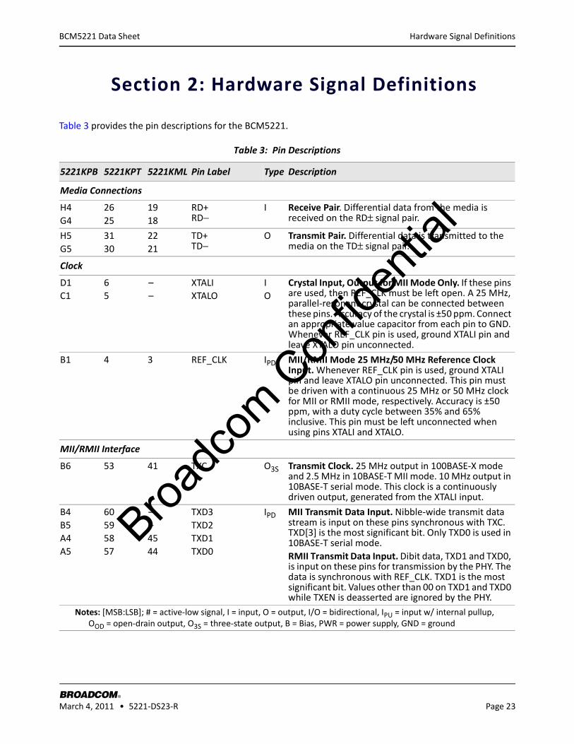
Table 3 provides the pin descriptions for the BCM5221.
Table 3: Pin Descriptions
5221KPB 5221KPT 5221KML Pin Label Type Description
Media Connections
H4G4
2625
1918
RD+ RD−
I Receive Pair. Differential data from the media is received on the RD± signal pair.
H5G5
3130
2221
TD+ TD−
O Transmit Pair. Differential data is transmitted to the media on the TD± signal pair.
Clock
D1C1
65
– –
XTALIXTALO
IO
Crystal Input, Output for MII Mode Only. If these pins are used, then REF_CLK must be left open. A 25 MHz, parallel-resonant crystal can be connected between these pins. Accuracy of the crystal is ±50 ppm. Connect an appropriate value capacitor from each pin to GND. Whenever REF_CLK pin is used, ground XTALI pin and leave XTALO pin unconnected.
B1 4 3 REF_CLK IPD MII/RMII Mode 25 MHz/50 MHz Reference Clock Input. Whenever REF_CLK pin is used, ground XTALI pin and leave XTALO pin unconnected. This pin must be driven with a continuous 25 MHz or 50 MHz clock for MII or RMII mode, respectively. Accuracy is ±50 ppm, with a duty cycle between 35% and 65% inclusive. This pin must be left unconnected when using pins XTALI and XTALO.
MII/RMII Interface
B6 53 41 TXC O3S Transmit Clock. 25 MHz output in 100BASE-X mode and 2.5 MHz in 10BASE-T MII mode. 10 MHz output in 10BASE-T serial mode. This clock is a continuously driven output, generated from the XTALI input.
B4B5A4A5
60595857
– – 4544
TXD3TXD2TXD1TXD0
IPD MII Transmit Data Input. Nibble-wide transmit data stream is input on these pins synchronous with TXC. TXD[3] is the most significant bit. Only TXD0 is used in 10BASE-T serial mode. RMII Transmit Data Input. Dibit data, TXD1 and TXD0, is input on these pins for transmission by the PHY. The data is synchronous with REF_CLK. TXD1 is the most significant bit. Values other than 00 on TXD1 and TXD0 while TXEN is deasserted are ignored by the PHY.
Notes: [MSB:LSB]; # = active-low signal, I = input, O = output, I/O = bidirectional, IPU = input w/ internal pullup, OOD = open-drain output, O3S = three-state output, B = Bias, PWR = power supply, GND = ground
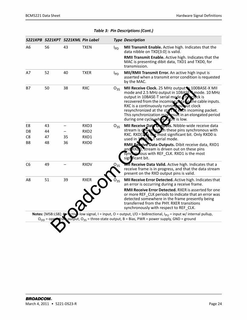
Broadc
om C
onfid
entia
l
Hardware Signal Definitions
BROADCOM March 4, 2011 • 5221-DS23-R Page 24
®
BCM5221 Data Sheet
A6 56 43 TXEN IPD MII Transmit Enable. Active high. Indicates that the data nibble on TXD[3:0] is valid.RMII Transmit Enable. Active high. Indicates that the MAC is presenting dibit data, TXD1 and TXD0, for transmission.
A7 52 40 TXER IPD MII/RMII Transmit Error. An active high input is asserted when a transmit error condition is requested by the MAC.
B7 50 38 RXC O3S MII Receive Clock. 25 MHz output in 100BASE-X MII mode and 2.5 MHz output in 10BASE-T mode. 10 MHz output in 10BASE-T serial mode. This clock is recovered from the incoming data on the cable inputs. RXC is a continuously running output clock resynchronized at the start of each incoming packet. This synchronization may result in an elongated period during one cycle while RXDV is low.
E8D8C8B8
43444748
– – 3536
RXD3RXD2RXD1RXD0
O3S MII Receive Data Outputs. Nibble-wide receive data stream is driven out on these pins synchronous with RXC. RXD[3] is the most significant bit. Only RXD0 is used in 10BASE-T serial mode.RMII Receive Data Outputs. Dibit receive data, RXD1 and RXD0, stream is driven out on these pins synchronous with REF_CLK. RXD1 is the most significant bit.
C6 49 – RXDV O3S MII Receive Data Valid. Active high. Indicates that a receive frame is in progress, and that the data stream present on the RXD output pins is valid.
A8 51 39 RXER O3S MII Receive Error Detected. Active high. Indicates that an error is occurring during a receive frame.RMII Receive Error Detected. RXER is asserted for one or more REF_CLK periods to indicate that an error was detected somewhere in the frame presently being transferred from the PHY. RXER transitions synchronously with respect to REF_CLK.
Table 3: Pin Descriptions (Cont.)
5221KPB 5221KPT 5221KML Pin Label Type Description
Notes: [MSB:LSB]; # = active-low signal, I = input, O = output, I/O = bidirectional, IPU = input w/ internal pullup, OOD = open-drain output, O3S = three-state output, B = Bias, PWR = power supply, GND = ground
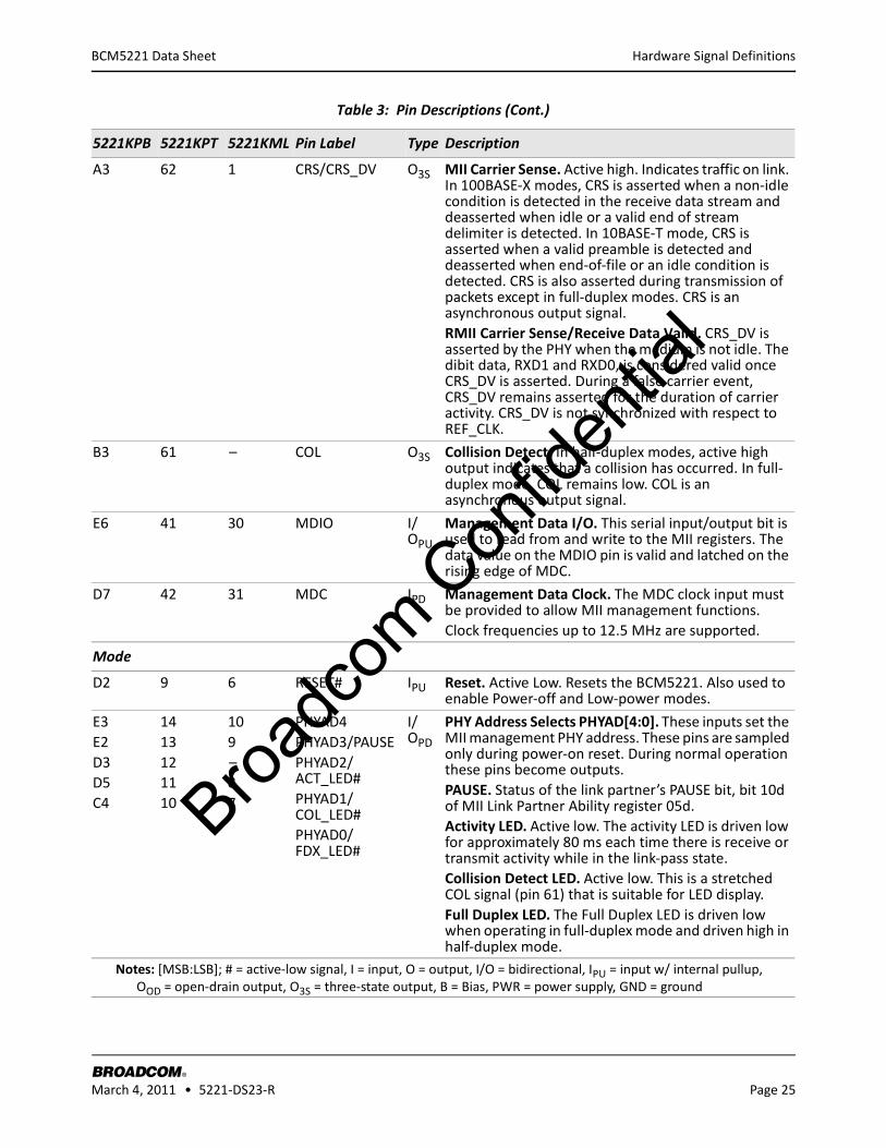
Broadc
om C
onfid
entia
l
Hardware Signal Definitions
BROADCOM March 4, 2011 • 5221-DS23-R Page 25
®
BCM5221 Data Sheet
A3 62 1 CRS/CRS_DV O3S MII Carrier Sense. Active high. Indicates traffic on link. In 100BASE-X modes, CRS is asserted when a non-idle condition is detected in the receive data stream and deasserted when idle or a valid end of stream delimiter is detected. In 10BASE-T mode, CRS is asserted when a valid preamble is detected and deasserted when end-of-file or an idle condition is detected. CRS is also asserted during transmission of packets except in full-duplex modes. CRS is an asynchronous output signal. RMII Carrier Sense/Receive Data Valid. CRS_DV is asserted by the PHY when the medium is not idle. The dibit data, RXD1 and RXD0, is considered valid once CRS_DV is asserted. During a false carrier event, CRS_DV remains asserted for the duration of carrier activity. CRS_DV is not synchronized with respect to REF_CLK.
B3 61 – COL O3S Collision Detect. In half-duplex modes, active high output indicates that a collision has occurred. In full-duplex mode, COL remains low. COL is an asynchronous output signal.
E6 41 30 MDIO I/OPU
Management Data I/O. This serial input/output bit is used to read from and write to the MII registers. The data value on the MDIO pin is valid and latched on the rising edge of MDC.
D7 42 31 MDC IPD Management Data Clock. The MDC clock input must be provided to allow MII management functions. Clock frequencies up to 12.5 MHz are supported.
Mode
D2 9 6 RESET# IPU Reset. Active Low. Resets the BCM5221. Also used to enable Power-off and Low-power modes.
E3E2D3D5C4
1413121110
109 – 87
PHYAD4PHYAD3/PAUSEPHYAD2/ACT_LED#PHYAD1/COL_LED#PHYAD0/FDX_LED#
I/OPD
PHY Address Selects PHYAD[4:0]. These inputs set the MII management PHY address. These pins are sampled only during power-on reset. During normal operation these pins become outputs.PAUSE. Status of the link partner’s PAUSE bit, bit 10d of MII Link Partner Ability register 05d.Activity LED. Active low. The activity LED is driven low for approximately 80 ms each time there is receive or transmit activity while in the link-pass state.Collision Detect LED. Active low. This is a stretched COL signal (pin 61) that is suitable for LED display.Full Duplex LED. The Full Duplex LED is driven low when operating in full-duplex mode and driven high in half-duplex mode.
Table 3: Pin Descriptions (Cont.)
5221KPB 5221KPT 5221KML Pin Label Type Description
Notes: [MSB:LSB]; # = active-low signal, I = input, O = output, I/O = bidirectional, IPU = input w/ internal pullup, OOD = open-drain output, O3S = three-state output, B = Bias, PWR = power supply, GND = ground
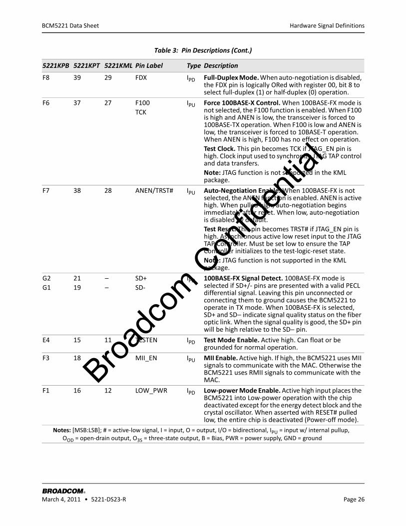
Broadc
om C
onfid
entia
l
Hardware Signal Definitions
BROADCOM March 4, 2011 • 5221-DS23-R Page 26
®
BCM5221 Data Sheet
F8 39 29 FDX IPD Full-Duplex Mode. When auto-negotiation is disabled, the FDX pin is logically ORed with register 00, bit 8 to select full-duplex (1) or half-duplex (0) operation.
F6 37 27 F100TCK
IPU Force 100BASE-X Control. When 100BASE-FX mode is not selected, the F100 function is enabled. When F100 is high and ANEN is low, the transceiver is forced to 100BASE-TX operation. When F100 is low and ANEN is low, the transceiver is forced to 10BASE-T operation. When ANEN is high, F100 has no effect on operation. Test Clock. This pin becomes TCK if JTAG_EN pin is high. Clock input used to synchronize JTAG TAP control and data transfers.Note: JTAG function is not supported in the KML package.
F7 38 28 ANEN/TRST# IPU Auto-Negotiation Enable. When 100BASE-FX is not selected, the ANEN function is enabled. ANEN is active high. When pulled high, auto-negotiation begins immediately after reset. When low, auto-negotiation is disabled by default. Test Reset. This pin becomes TRST# if JTAG_EN pin is high. Asynchronous active low reset input to the JTAG TAP Controller. Must be set low to ensure the TAP Controller initializes to the test-logic-reset state.Note: JTAG function is not supported in the KML package.
G2G1
2119
– –
SD+SD-
IPD 100BASE-FX Signal Detect. 100BASE-FX mode is selected if SD+/- pins are presented with a valid PECL differential signal. Leaving this pin unconnected or connecting them to ground causes the BCM5221 to operate in TX mode. When 100BASE-FX is selected, SD+ and SD− indicate signal quality status on the fiber optic link. When the signal quality is good, the SD+ pin will be high relative to the SD− pin.
E4 15 11 TESTEN IPD Test Mode Enable. Active high. Can float or be grounded for normal operation.
F3 18 – MII_EN IPU MII Enable. Active high. If high, the BCM5221 uses MII signals to communicate with the MAC. Otherwise the BCM5221 uses RMII signals to communicate with the MAC.
F1 16 12 LOW_PWR IPD Low-power Mode Enable. Active high input places the BCM5221 into Low-power operation with the chip deactivated except for the energy detect block and the crystal oscillator. When asserted with RESET# pulled low, the entire chip is deactivated (Power-off mode).
Table 3: Pin Descriptions (Cont.)
5221KPB 5221KPT 5221KML Pin Label Type Description
Notes: [MSB:LSB]; # = active-low signal, I = input, O = output, I/O = bidirectional, IPU = input w/ internal pullup, OOD = open-drain output, O3S = three-state output, B = Bias, PWR = power supply, GND = ground
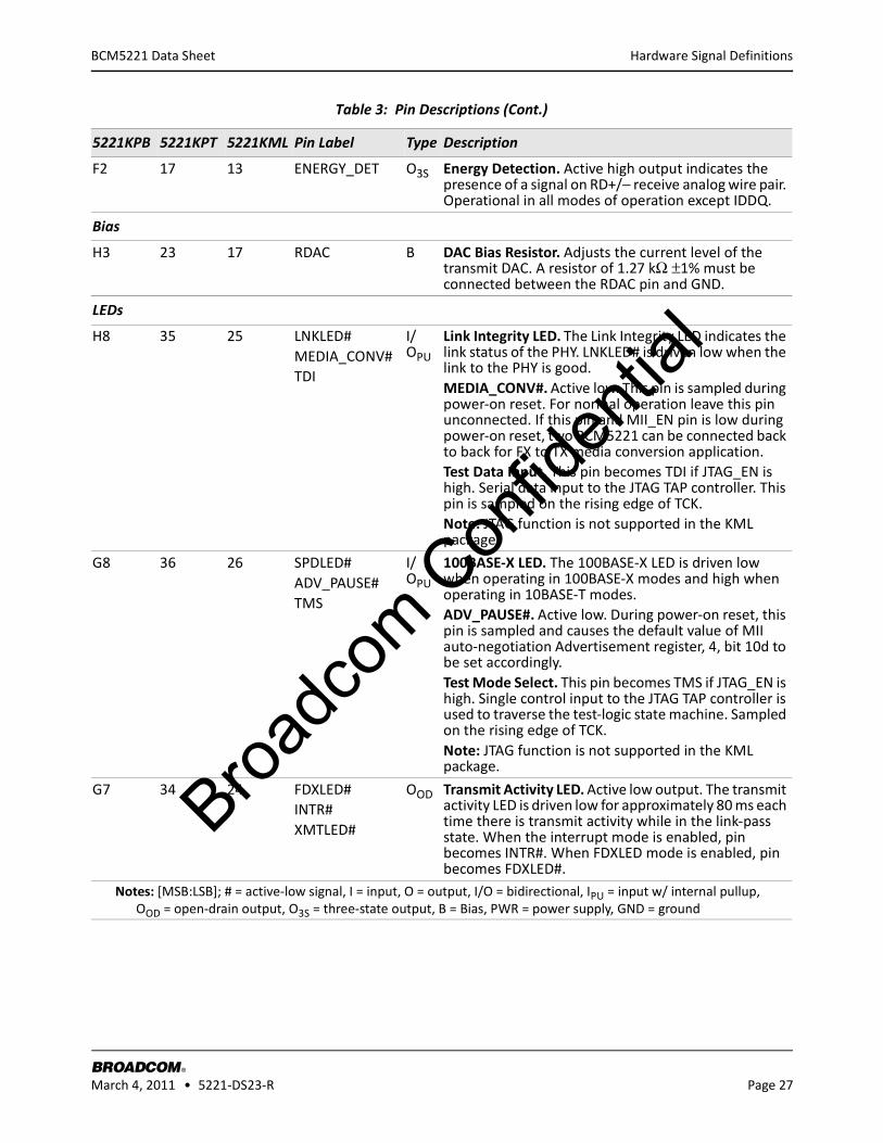
Broadc
om C
onfid
entia
l
Hardware Signal Definitions
BROADCOM March 4, 2011 • 5221-DS23-R Page 27
®
BCM5221 Data Sheet
F2 17 13 ENERGY_DET O3S Energy Detection. Active high output indicates the presence of a signal on RD+/− receive analog wire pair. Operational in all modes of operation except IDDQ.
Bias
H3 23 17 RDAC B DAC Bias Resistor. Adjusts the current level of the transmit DAC. A resistor of 1.27 kΩ ±1% must be connected between the RDAC pin and GND.
LEDs
H8 35 25 LNKLED#MEDIA_CONV#TDI
I/OPU
Link Integrity LED. The Link Integrity LED indicates the link status of the PHY. LNKLED# is driven low when the link to the PHY is good.MEDIA_CONV#. Active low. This pin is sampled during power-on reset. For normal operation leave this pin unconnected. If this pin and MII_EN pin is low during power-on reset, two BCM5221 can be connected back to back for FX to TX media conversion application. Test Data Input. This pin becomes TDI if JTAG_EN is high. Serial data input to the JTAG TAP controller. This pin is sampled on the rising edge of TCK.Note: JTAG function is not supported in the KML package.
G8 36 26 SPDLED#ADV_PAUSE#TMS
I/OPU
100BASE-X LED. The 100BASE-X LED is driven low when operating in 100BASE-X modes and high when operating in 10BASE-T modes.ADV_PAUSE#. Active low. During power-on reset, this pin is sampled and causes the default value of MII auto-negotiation Advertisement register, 4, bit 10d to be set accordingly.Test Mode Select. This pin becomes TMS if JTAG_EN is high. Single control input to the JTAG TAP controller is used to traverse the test-logic state machine. Sampled on the rising edge of TCK.Note: JTAG function is not supported in the KML package.
G7 34 24 FDXLED#INTR#XMTLED#
OOD Transmit Activity LED. Active low output. The transmit activity LED is driven low for approximately 80 ms each time there is transmit activity while in the link-pass state. When the interrupt mode is enabled, pin becomes INTR#. When FDXLED mode is enabled, pin becomes FDXLED#.
Table 3: Pin Descriptions (Cont.)
5221KPB 5221KPT 5221KML Pin Label Type Description
Notes: [MSB:LSB]; # = active-low signal, I = input, O = output, I/O = bidirectional, IPU = input w/ internal pullup, OOD = open-drain output, O3S = three-state output, B = Bias, PWR = power supply, GND = ground
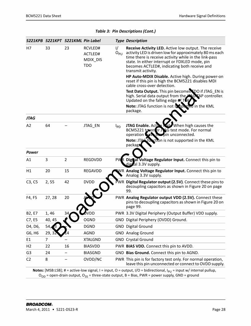
Broadc
om C
onfid
entia
l
Hardware Signal Definitions
BROADCOM March 4, 2011 • 5221-DS23-R Page 28
®
BCM5221 Data Sheet
H7 33 23 RCVLED#ACTLED#MDIX_DISTDO
I/OPU
Receive Activity LED. Active low output. The receive activity LED is driven low for approximately 80 ms each time there is receive activity while in the link-pass state. In either interrupt or FDXLED mode, pin becomes ACTLED#, indicating both receive and transmit activity.HP Auto-MDIX Disable. Active high. During power-on reset if this pin is high the BCM5221 disables MDI cable cross-over detection.Test Data Output. This pin becomes TDO if JTAG_EN is high. Serial data output from the JTAG TAP controller. Updated on the falling edge of TCK.Note: JTAG function is not supported in the KML package.
JTAG
A2 64 – JTAG_EN IPD JTAG Enable. Active high. When high causes the BCM5221 to enter JTAG test mode. For normal operation leave this pin unconnected.Note: JTAG function is not supported in the KML package.
Power
A1 3 2 REGDVDD PWR Digital Voltage Regulator Input. Connect this pin to digital 3.3V supply.
H1 20 15 REGAVDD PWR Analog Voltage Regulator Input. Connect this pin to Analog 3.3V supply.
C3, C5 2, 55 42 DVDD PWR Digital Regulator output (2.5V). Connect these pins to decoupling capacitors as shown in Figure 20 on page 99.
F4, F5 27, 28 20 AVDD PWR Analog Regulator output VDD (2.5V). Connect these pins to decoupling capacitors as shown in Figure 20 on page 99.
B2, E7 1, 46 34 OVDD PWR 3.3V Digital Periphery (Output Buffer) VDD supply.
C7, E5 40, 45 – OGND GND Digital Periphery (OVDD) Ground.
D4, D6, 54, 63 – DGND GND Digital Ground
G6, H6 29, 32 14 AGND GND Analog Ground
E1 7 – XTALGND GND Crystal Ground
H2 22 16 BIASVDD PWR BIAS VDD. Connect this pin to AVDD.
G3 24 – BIASGND GND Bias Ground. Connect this pin to AGND.
C2 8 – OVDD/NC PWR This pin is for factory test only. For normal operation, leave this pin unconnected or connect to OVDD supply.
Table 3: Pin Descriptions (Cont.)
5221KPB 5221KPT 5221KML Pin Label Type Description
Notes: [MSB:LSB]; # = active-low signal, I = input, O = output, I/O = bidirectional, IPU = input w/ internal pullup, OOD = open-drain output, O3S = three-state output, B = Bias, PWR = power supply, GND = ground
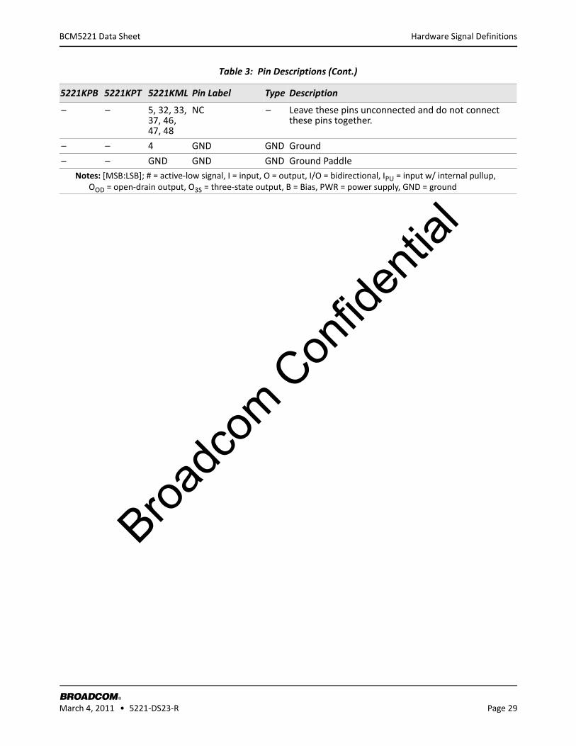
Broadc
om C
onfid
entia
l
Hardware Signal Definitions
BROADCOM March 4, 2011 • 5221-DS23-R Page 29
®
BCM5221 Data Sheet
– – 5, 32, 33, 37, 46, 47, 48
NC – Leave these pins unconnected and do not connect these pins together.
– – 4 GND GND Ground
– – GND GND GND Ground Paddle
Table 3: Pin Descriptions (Cont.)
5221KPB 5221KPT 5221KML Pin Label Type Description
Notes: [MSB:LSB]; # = active-low signal, I = input, O = output, I/O = bidirectional, IPU = input w/ internal pullup, OOD = open-drain output, O3S = three-state output, B = Bias, PWR = power supply, GND = ground
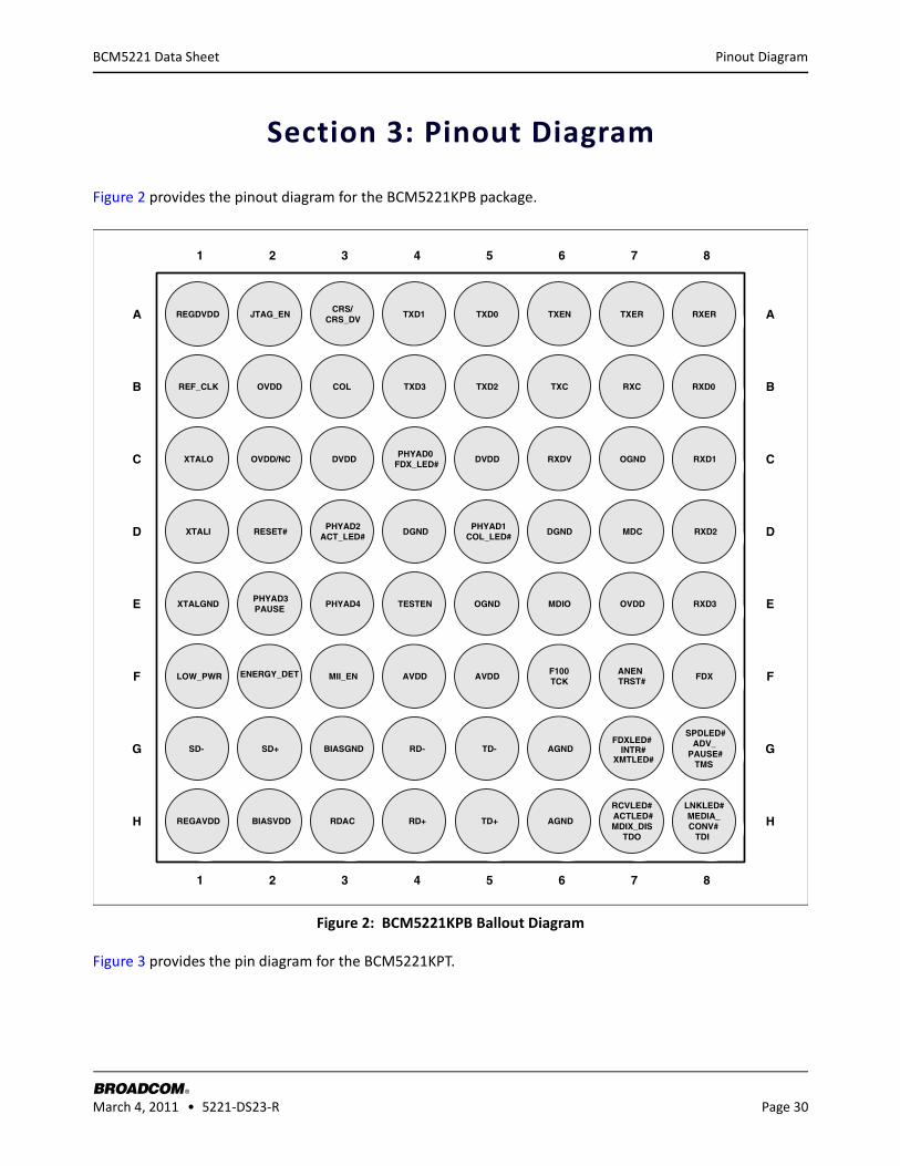
Broadc
om C
onfid
entia
l
Pinout Diagram
BROADCOM March 4, 2011 • 5221-DS23-R Page 30
®
BCM5221 Data Sheet
Section 3: Pinout Diagram
Figure 2 provides the pinout diagram for the BCM5221KPB package.
Figure 2: BCM5221KPB Ballout Diagram
Figure 3 provides the pin diagram for the BCM5221KPT.
REGDVDD JTAG_ENCRS/
CRS_DVTXD1 TXD0 TXEN TXER RXER
REF_CLK OVDD COL TXD3 TXD2 TXC RXC RXD0
XTALO OVDD/NC DVDDPHYAD0
FDX_LED# DVDD RXDV OGND RXD1
XTALI RESET#PHYAD2
ACT_LED# DGNDPHYAD1
COL_LED# DGND MDC RXD2
XTALGNDPHYAD3PAUSE PHYAD4 TESTEN OGND MDIO OVDD RXD3
LOW_PWR ENERGY_DET MII_EN AVDD AVDDF100TCK
ANENTRST# FDX
SD- SD+ BIASGND RD- TD- AGNDXMTLED#
INTR#FDXLED#
SPDLED#ADV_
PAUSE#TMS
REGAVDD BIASVDD RDAC RD+ TD+ AGND
RCVLED#ACTLED#MDIX_DIS
TDO
LNKLED#MEDIA_CONV#
TDI
B
A
C
D
E
F
G
H
1 2 3 4 5 6 7 8
1 2 3 4 5 6 7 8
B
A
C
D
E
F
G
H
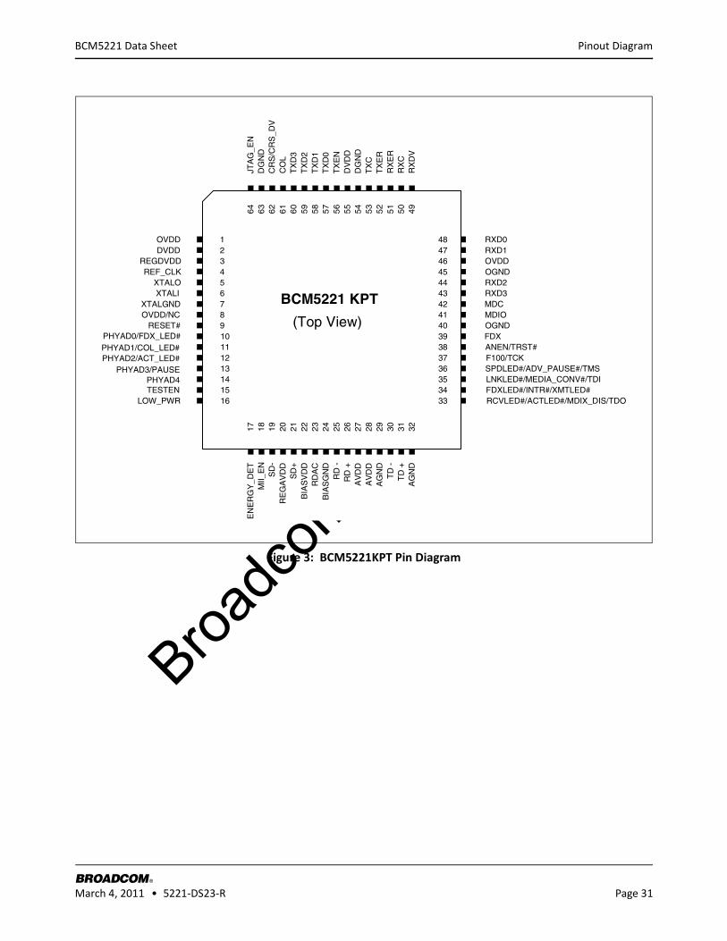
Broadc
om C
onfid
entia
l
Pinout Diagram
BROADCOM March 4, 2011 • 5221-DS23-R Page 31
®
BCM5221 Data Sheet
Figure 3: BCM5221KPT Pin Diagram
SD
-R
EG
AV
DD
SD
+B
IAS
VD
D
RD
+
TD
+
BIA
SG
ND
RD
-
RD
AC
TD
-
AV
DD
AG
ND
AV
DD
TX
D1
TX
D0
RX
DV
RX
C
TX
D2
AG
ND
ANEN/TRST#
RXD3MDC
F100/TCK
TX
D3
DG
ND
CR
S/C
RS
_DV
JTA
G_E
N
CO
L
TX
ER
RX
ER
TX
CD
GN
D
TX
EN
DV
DD
RXD0RXD1
PHYAD4
RESET#OVDD/NC
TESTEN
OVDDDVDD
REGDVDDREF_CLK
XTALIXTALGND
LOW_PWR
PHYAD3/PAUSE
PHYAD1/COL_LED#PHYAD2/ACT_LED#
PHYAD0/FDX_LED#
OVDD
OGND
RXD2OGND
EN
ER
GY
_DE
TM
II_E
N
RCVLED#/ACTLED#/MDIX_DIS/TDO
SPDLED#/ADV_PAUSE#/TMS
FDXLED#/INTR#/XMTLED#LNKLED#/MEDIA_CONV#/TDI
MDIO
FDX
BCM5221 KPT
464748
45
38
34
44
36
4243
35
37
4039
33
41
21
43
65
87
109
1211
1413
1615
1817 2019 2221 2423 2625 2827 3029 3231
6264 6061 5859 5657 545563 53 5152 4950
(Top View)
XTALO
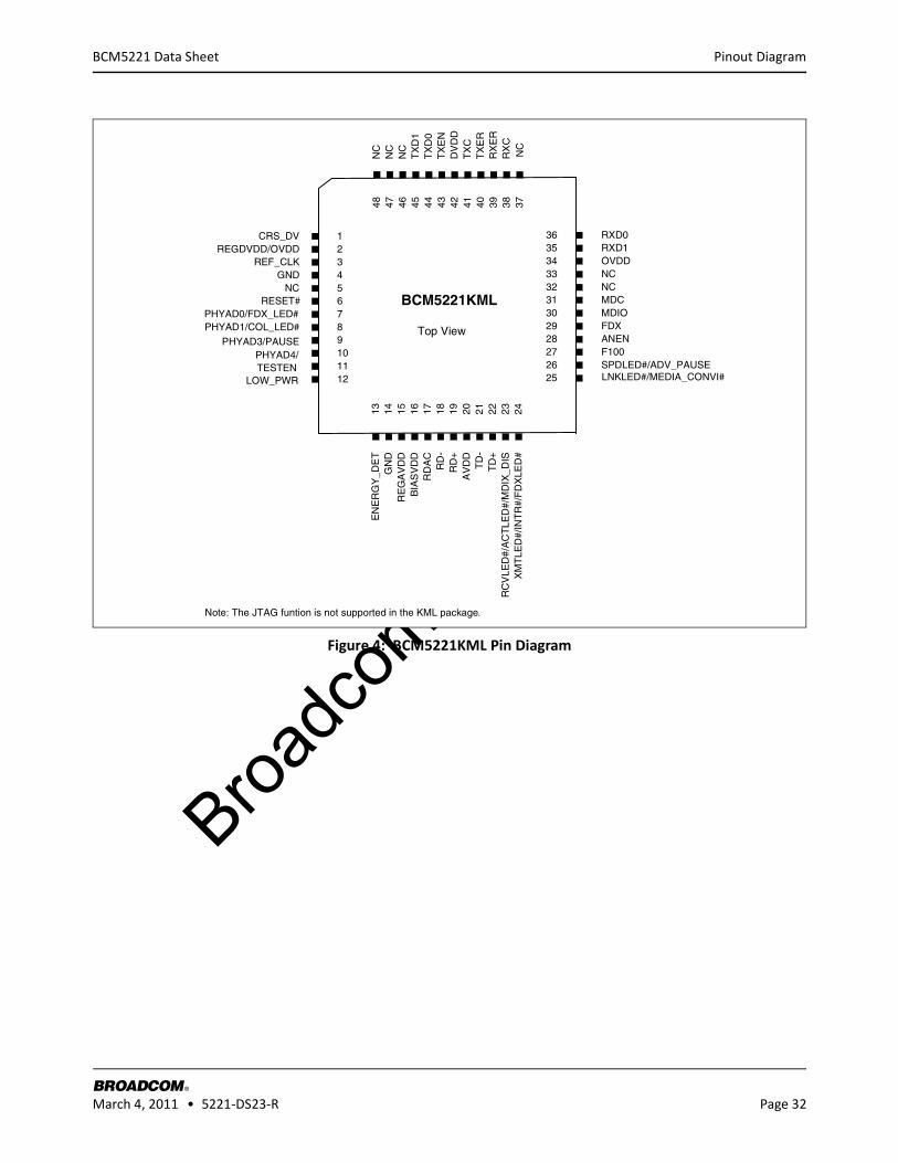
Broadc
om C
onfid
entia
l
Pinout Diagram
BROADCOM March 4, 2011 • 5221-DS23-R Page 32
®
BCM5221 Data Sheet
Figure 4: BCM5221KML Pin Diagram
RE
GA
VD
DB
IAS
VD
DR
DA
CR
D-
TD
+
AV
DD
TD
-
RD
+
XM
TLE
D#/
INT
R#/
FD
XLE
D#
RC
VLE
D#/
AC
TLE
D#/
MD
IX_D
IS
DV
DD
TX
C
TX
EN
SPDLED#/ADV_PAUSE
MDCMDIO
LNKLED#/MEDIA_CONVI#
TX
D0
NC
NC
NC
TX
D1
NC
RX
C
TX
ER
RX
ER
RXD0RXD1
PHYAD3/PAUSE
PHYAD1/COL_LED#
CRS_DVREGDVDD/OVDD
REF_CLKGND
RESET#
PHYAD0/FDX_LED#
TESTENLOW_PWR
PHYAD4/
OVDD
ANEN
NCNC
EN
ER
GY
_DE
TG
ND
FDX
F100
BCM5221KML
343536
33
26
32
3031
25
2827
29
21
43
65
87
109
1211
1413 1615 1817 2019 2221 2423
4648 4445 4243 4041 383947 37
Top View
NC
Note: The JTAG funtion is not supported in the KML package.
Broadc
om C
onfid
entia
l
Operational Description
BROADCOM March 4, 2011 • 5221-DS23-R Page 33
®
BCM5221 Data Sheet
Section 4: Operational Description
ResetThere are two ways to reset the BCM5221. A hardware reset pin is provided that resets all internal nodes in the chip to a known state. RESET# pin must be held low when powering the BCM5221 to get the chip into normal mode. If the BCM5221 is not provided a power on reset, it is possible for the chip to power up in a low-power mode. To exit this low-power mode, RESET# pin must be held low for at least 20 μs. Hardware reset should always be applied to the BCM5221 after power-up.
The BCM5221 also has a software reset capability. To perform software reset, 1 must be written to bit 15 of the MII Control register. This bit is self-clearing, meaning that a second write operation is not necessary to end the reset. There is no effect if 0 is written to the MII Control register reset bit.
The BCM5221 clock input can be driven two ways: internal crystal oscillator or external oscillator. To take advantage of the internal oscillator, attach a 25 MHz crystal between the XTALI and XTALO pins. Connect 27 pF capacitors from each pin to ground. Alternatively, a 50% duty cycle 25 MHz clock can be directly applied to the XTALI pin. In this case, the XTALO output must be left unconnected. No capacitors are used.
Isolate ModeWhen the BCM5221 is put into isolate mode, all MII inputs (TXD[3:0], TXEN, and TXER) are ignored, and all MII outputs (TXC, COL, CRS, RXC, RXDV, RXER, and RXD[3:0]) are set to high impedance. MII management pins (MDC, MDIO), TD± and RD± pins operate normally. Writing 1 to bit 10 of the MII Control register puts the port into isolate mode. Writing 0 to the same bit removes it from isolate mode. Upon resetting the chip through hardware or software, the isolate mode is off.
Super Isolate ModeWhen the chip is in super isolate mode, in addition to Isolate mode actions, the chip also sets TD± pins to high impedance. Writing 1 to bit 3 of the MII register 1Eh puts the port into super isolate mode. Writing 0 to the same bit removes it from super isolate mode. Upon resetting the chip through hardware or software, the isolate mode is off.
Broadc
om C
onfid
entia
l
Loopback Mode
BROADCOM March 4, 2011 • 5221-DS23-R Page 34
®
BCM5221 Data Sheet
Loopback ModeLoopback mode allows in-circuit testing of the BCM5221 chip. All packets sent in through the TXD pins are looped-back internally to the RXD pins, and are not sent out to the cable. The loopback mode is enabled by writing 1 to bit 14 of the MII Control register. To resume normal operation, bit 14 of the MII Control register must be 0.
Incoming packets on the cable are ignored in loopback mode. Because of this, the COL pin is normally not activated during loopback mode. To test that the COL pin is actually working, the BCM5221 can be placed into collision test mode. This mode is enabled by writing 1 to bit 7 of the MII Control register. Asserting TXEN causes the COL output to go high, and deasserting TXEN causes the COL output to go low.
Full-Duplex ModeThe BCM5221 supports full-duplex operation. While in full-duplex mode, a transceiver can simultaneously transmit and receive packets on the cable. The COL signal is never activated when in full-duplex mode. The CRS output is asserted only during receive packets, not transmit packets.
By default, the BCM5221 powers up in half-duplex mode. When auto-negotiation is disabled, full-duplex operation can be enabled either by FDX pin control or by an MII register bit (Register 0, bit 8).
When auto-negotiation is enabled in DTE mode, full-duplex capability is advertised by default, but can be overridden by a write to the auto-negotiation Advertisement register (04h).
One of the LED outputs can be modified to signal full-duplex versus half-duplex operation. This capability is enabled by setting MII register 1Ah, bit 15. In this mode, XMTLED# becomes FDXLED#, where 1 output indicates half-duplex and 0 output indicates full-duplex. This value is the inverse of MII register 18h, bit 0. When the FDXLED mode is activated, the RCVLED# becomes ACTLED#.
100BASE-FX ModeFor 100BASE-FX mode, the BCM5221 transceiver interfaces with an external 100BASE-FX fiber-optic driver and receiver instead of the magnetics module used with twisted-pair cable. The differential transmit and receive data pairs operate at PECL voltage levels instead of those required for twisted-pair transmission. The data stream is encoded using two-level NRZI instead of three-level MLT3. Since scrambling is not used in 100BASE-FX operation, the stream cipher function is bypassed.
The external fiber-optic receiver detects signal status and passes it into the BCM5221 through the SD± pins. The SD± pins select the 100BASE-FX mode.
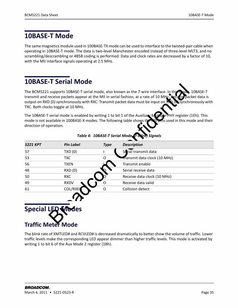
Broadc
om C
onfid
entia
l
10BASE-T Mode
BROADCOM March 4, 2011 • 5221-DS23-R Page 35
®
BCM5221 Data Sheet
10BASE-T ModeThe same magnetics module used in 100BASE-TX mode can be used to interface to the twisted-pair cable when operating in 10BASE-T mode. The data is two-level Manchester encoded instead of three-level MLT3, and no scrambling/descrambling or 4B5B coding is performed. Data and clock rates are decreased by a factor of 10, with the MII interface signals operating at 2.5 MHz.
10BASE-T Serial ModeThe BCM5221 supports 10BASE-T serial mode, also known as the 7-wire interface. In this mode, 10BASE-T transmit and receive packets appear at the MII in serial fashion, at a rate of 10 MHz. Receive packet data is output on RXD (0) synchronously with RXC. Transmit packet data must be input on TXD (0) synchronously with TXC. Both clocks toggle at 10 MHz.
The 10BASE-T serial mode is enabled by writing 1 to bit 1 of the Auxiliary Multiple-PHY register (1Eh). This mode is not available in 100BASE-X modes. The following table shows the MII pins used in this mode and their direction of operation.
Special LED Modes
Traffic Meter ModeThe blink rate of XMTLED# and RCVLED# is decreased dramatically to better show the volume of traffic. Lower traffic levels make the corresponding LED appear dimmer than higher traffic levels. This mode is activated by writing 1 to bit 6 of the Aux Mode 2 register (1Bh).
Table 4: 10BASE-T Serial Mode (7-Wire) Signals
5221 KPT Pin Label Type Description
57 TXD (0) I Serial transmit data
53 TXC O Transmit data clock (10 MHz)
56 TXEN I Transmit enable
48 RXD (0) O Serial receive data
50 RXC O Receive data clock (10 MHz)
49 RXDV O Receive data valid
61 COL/RXEN O Collision detect

Broadc
om C
onfid
entia
l
Interrupt Mode
BROADCOM March 4, 2011 • 5221-DS23-R Page 36
®
BCM5221 Data Sheet
Force LEDs OnThe SPDLED#, LNKLED#, XMTLED#, RCVLED#, COL_LED#, ACT_LED#, and FDX_LED# outputs can be forced on (0 value) by writing 01 to bit 5 and 4 of shadow register 1Ah.
Disable LEDsThe SPDLED#, LNKLED#, XMTLED#, RCVLED#, COL_LED#, ACT_LED#, and FDX_LED# outputs can be forced off (1 value) by writing a 10 to bit 5 and 4 of shadow register 1Ah.
Interrupt ModeThe BCM5221 can be programmed to provide an interrupt output. Three conditions can cause an interrupt to be generated: changes in the duplex mode, changes in the speed of operation or changes in the link status. The interrupt feature is disabled by default. When the interrupt capability is enabled by setting MII register 1Ah, bit 14, the XMTLED# pin becomes the INTR# pin and the RCVLED# pin becomes an activity pin named ACTLED#. The INTR# pin is open-drain and can be wire-ORed with INTR# pins of other chips on a board. The status of each interrupt source is reflected in register 1Ah, bits 1, 2, and 3. If any type of interrupt occurs, the Interrupt Status bit, register 1Ah, bit 0, is set.
The Interrupt register (1Ah) also contains several bits to control different facets of the interrupt function. If the interrupt enable bit is set to 0, no status bits are set and no interrupts are generated. If the interrupt enable bit is set to 1, the following conditions apply:
• If mask status bits (bits 9,10,11) are set to 0 and the interrupt mask (bit 8) is set to 0, status bits and interrupts are available.
• If mask status bits (bits 9,10,11) are set to 0 and the interrupt mask (bit 8) is set to 1, status bits are set but no interrupts are generated.
• If any mask status bit is set to 1 and the interrupt mask is set to 0, that status bit is not set and no interrupt of that type is generated.
• If any mask status bit is set to 1 and the interrupt mask is set to 1, that status bit is not set and no interrupt of any kind is generated.
Energy DetectionAn on-chip energy detection circuit can determine when a link partner is connected to the end of the transmission media. The circuit monitors the receive inputs for any type of energy, including 10BASE-T, 100BASE-TX or 100BASE-FX packets, and 10BASE-T or auto-negotiation link pulses. When energy is detected on the receive inputs for longer than 1.3 ms, the ENERGYDET output is asserted. If all traces of energy disappear for longer then 1.3s, it is assumed that the link partner has disconnected, and the ENERGYDET output is deasserted. The energy detection circuit is operational in both full-power and some of the low-power modes.
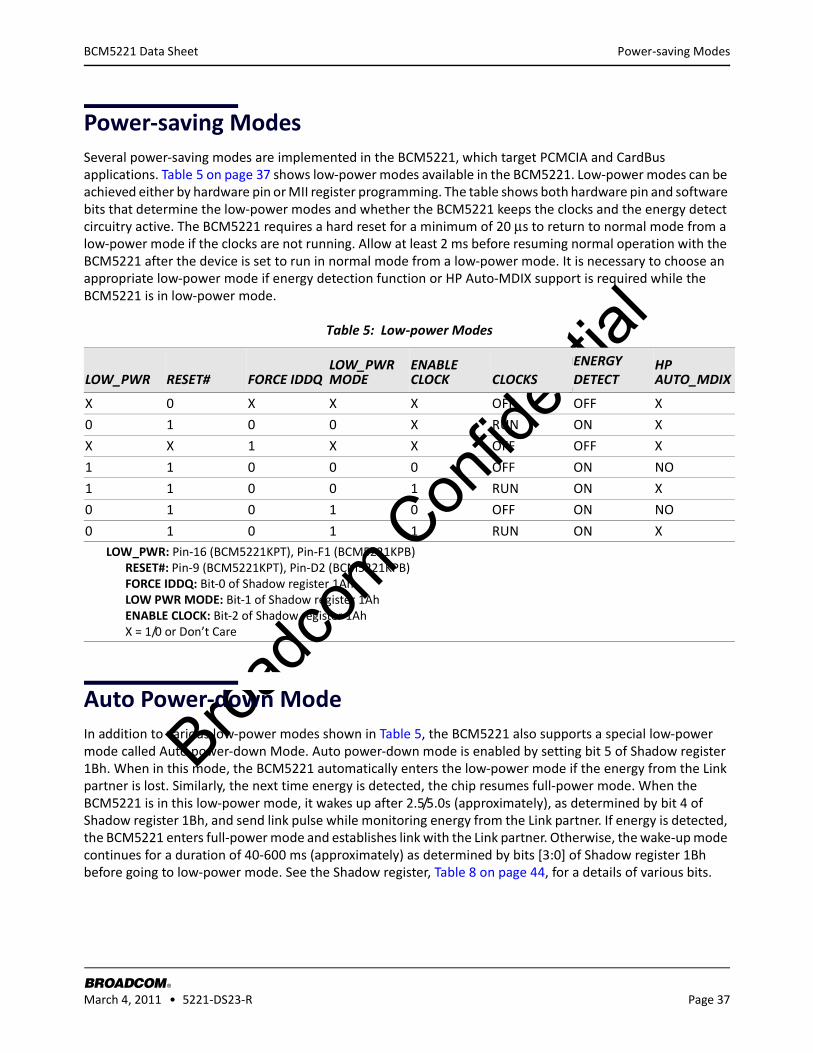
Broadc
om C
onfid
entia
l
Power-saving Modes
BROADCOM March 4, 2011 • 5221-DS23-R Page 37
®
BCM5221 Data Sheet
Power-saving ModesSeveral power-saving modes are implemented in the BCM5221, which target PCMCIA and CardBus applications. Table 5 on page 37 shows low-power modes available in the BCM5221. Low-power modes can be achieved either by hardware pin or MII register programming. The table shows both hardware pin and software bits that determine the low-power modes and whether the BCM5221 keeps the clocks and the energy detect circuitry active. The BCM5221 requires a hard reset for a minimum of 20 μs to return to normal mode from a low-power mode if the clocks are not running. Allow at least 2 ms before resuming normal operation with the BCM5221 after the device is set to run in normal mode from a low-power mode. It is necessary to choose an appropriate low-power mode if energy detection function or HP Auto-MDIX support is required while the BCM5221 is in low-power mode.
Auto Power-down ModeIn addition to various low-power modes shown in Table 5, the BCM5221 also supports a special low-power mode called Auto power-down Mode. Auto power-down mode is enabled by setting bit 5 of Shadow register 1Bh. When in this mode, the BCM5221 automatically enters the low-power mode if the energy from the Link partner is lost. Similarly, the next time energy is detected, the chip resumes full-power mode. When the BCM5221 is in this low-power mode, it wakes up after 2.5/5.0s (approximately), as determined by bit 4 of Shadow register 1Bh, and send link pulse while monitoring energy from the Link partner. If energy is detected, the BCM5221 enters full-power mode and establishes link with the Link partner. Otherwise, the wake-up mode continues for a duration of 40-600 ms (approximately) as determined by bits [3:0] of Shadow register 1Bh before going to low-power mode. See the Shadow register, Table 8 on page 44, for a details of various bits.
Table 5: Low-power Modes
LOW_PWR RESET# FORCE IDDQLOW_PWR MODE
ENABLE CLOCK CLOCKS
ENERGYDETECT
HP AUTO_MDIX
X 0 X X X OFF OFF X
0 1 0 0 X RUN ON X
X X 1 X X OFF OFF X
1 1 0 0 0 OFF ON NO
1 1 0 0 1 RUN ON X
0 1 0 1 0 OFF ON NO
0 1 0 1 1 RUN ON XLOW_PWR: Pin-16 (BCM5221KPT), Pin-F1 (BCM5221KPB)
RESET#: Pin-9 (BCM5221KPT), Pin-D2 (BCM5221KPB) FORCE IDDQ: Bit-0 of Shadow register 1Ah LOW PWR MODE: Bit-1 of Shadow register 1Ah ENABLE CLOCK: Bit-2 of Shadow register 1Ah X = 1/0 or Don’t Care

Broadc
om C
onfid
entia
l
HP Auto-MDIX
BROADCOM March 4, 2011 • 5221-DS23-R Page 38
®
BCM5221 Data Sheet
HP Auto-MDIXDuring auto-negotiation and in various operating modes, one end of the link must be configured as an MDI (Media Independent Interface) crossover so that each transceiver’s transmitter is connected to the other’s receiver. The BCM5221 contains the ability to perform HP Auto-MDIX crossover, thus eliminating the need for crossover cable or cross-wired (MDIX) ports.
During Auto-Negotiation and in various operating modes, the BCM5221 normally transmits on TD± and receives on RD±. When connected via a straight-through cable to another device that does not have HP Auto-MDIX feature, the BCM5221 automatically switches its transmitter to RD± and its receiver to TD± in order to communicate with that device. If the link partner also has HP Auto-MDIX feature, then a random algorithm determines which end performs the crossover function.
The HP Auto-MDIX feature is implemented in accordance with the IEEE 802.3ab specification. The HP Auto-MDIX crossover feature is a function of Auto-Negotiation. Therefore if the BCM5221 is configured not to perform Auto-Negotiation, the feature will not work, and a specific cable will be required to ensure that each transceiver’s transmitter is connected to the other’s receiver.
The HP Auto-MDIX feature is enabled in hardware by pulling MDIX_DIS pin low during power on reset. If enabled by hardware, this feature can be disabled by setting bit 11 of MII register 1Ch to 0.
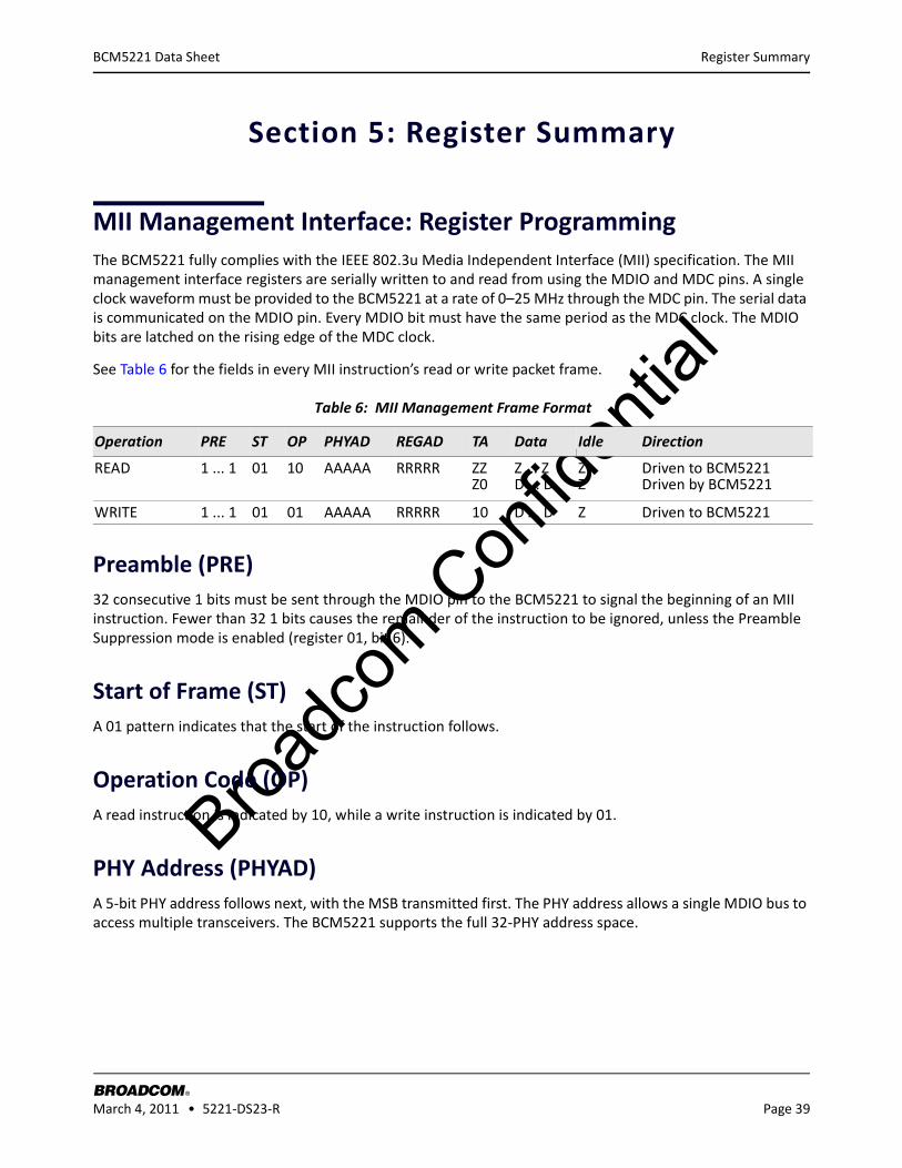
Broadc
om C
onfid
entia
l
Register Summary
BROADCOM March 4, 2011 • 5221-DS23-R Page 39
®
BCM5221 Data Sheet
Section 5: Register Summary
MII Management Interface: Register Programming The BCM5221 fully complies with the IEEE 802.3u Media Independent Interface (MII) specification. The MII management interface registers are serially written to and read from using the MDIO and MDC pins. A single clock waveform must be provided to the BCM5221 at a rate of 0–25 MHz through the MDC pin. The serial data is communicated on the MDIO pin. Every MDIO bit must have the same period as the MDC clock. The MDIO bits are latched on the rising edge of the MDC clock.
See Table 6 for the fields in every MII instruction’s read or write packet frame.
Preamble (PRE)32 consecutive 1 bits must be sent through the MDIO pin to the BCM5221 to signal the beginning of an MII instruction. Fewer than 32 1 bits causes the remainder of the instruction to be ignored, unless the Preamble Suppression mode is enabled (register 01, bit 6).
Start of Frame (ST)A 01 pattern indicates that the start of the instruction follows.
Operation Code (OP)A read instruction is indicated by 10, while a write instruction is indicated by 01.
PHY Address (PHYAD)A 5-bit PHY address follows next, with the MSB transmitted first. The PHY address allows a single MDIO bus to access multiple transceivers. The BCM5221 supports the full 32-PHY address space.
Table 6: MII Management Frame Format
Operation PRE ST OP PHYAD REGAD TA Data Idle Direction
READ 1 ... 1 01 10 AAAAA RRRRR ZZ Z0
Z ... Z D ... D
Z Z
Driven to BCM5221 Driven by BCM5221
WRITE 1 ... 1 01 01 AAAAA RRRRR 10 D ... D Z Driven to BCM5221
Broadc
om C
onfid
entia
l
MII Management Interface: Register Programming
BROADCOM March 4, 2011 • 5221-DS23-R Page 40
®
BCM5221 Data Sheet
Register Address (REGAD)A 5-bit register Address follows, with the MSB transmitted first. The register map of the BCM5221, containing register addresses and bit definitions, is provided on the following pages.
Turnaround (TA)The next two bit times are used to avoid contention on the MDIO pin when a read operation is performed. For a write operation, 10 must be sent to the chip during these two bit times. For a read operation, the MDIO pin must be placed into high-impedance during these two bit times. The chip drives the MDIO pin to 0 during the second bit time.
DataThe last 16 bits of the frame are the actual data bits. For a write operation, these bits are sent to the BCM5221. For a read operation, these bits are driven by the BCM5221. In either case, the MSB is transmitted first.
When writing to the BCM5221, the data field bits must be stable 10 ns before the rising-edge of MDC, and must be held valid for 10 ns after the rising edge of MDC. When reading from the BCM5221, the data field bits are valid after the rising edge of MDC until the next rising edge of MDC.
IdleA high-impedance state of the MDIO line. All drivers are disabled and the PHY’s pullup resistor pulls the line high. At least one or more clocked idle states are required between frames. Following are two examples of MII write and read instructions.
To put a chip with PHY address 00001 into loopback mode, the following MII write instruction must be issued:
1111 1111 1111 1111 1111 1111 1111 1111 0101 00001 00000 10 0100 0000 0000 0000 1...
To determine whether a PHY is in the link-pass state, the following MII read instruction must be issued:
1111 1111 1111 1111 1111 1111 1111 1111 0110 00001 00001 ZZ ZZZZ ZZZZ ZZZZ ZZZZ 1...
For the MII read operation, the BCM5221 drives the MDIO line during the TA and Data fields (the last 17 bit times). A final 65th clock pulse must be sent to close the transaction and cause a write operation.
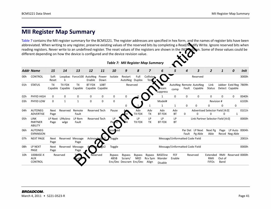
Broadc
om C
onfid
entia
l
BROADCOM March 4, 2011 • 5221-DS23-R Page 41
®
MII Register Map SummaryBCM5221 Data Sheet
MII Register Map SummaryTable 7 contains the MII register summary for the BCM5221. The register addresses are specified in hex form, and the names of register bits have been abbreviated. When writing to any register, preserve existing values of the reserved bits by completing a Read/Modify Write. Ignore reserved bits when reading registers. Never write to an undefined register. The reset values of the registers are shown in the INIT column. Some of these values could be different depending on how the device is configured and the device revision value.
Table 7: MII Register Map Summary
Addr Name 15 14 13 12 11 10 9 8 7 6 5 4 3 2 1 0 Init
00h CONTROL SoftReset
Loopback
Force100 AutoNegEnable
PowerDown
Isolate RestartAutoNeg
FullDuplex
CollisionTest
Reserved 3000h
01h STATUS T4Capable
TX FDXCapable
TXCapable
BT FDXCapable
10BTCapable
Reserved MF pream
suppress
AutoNeg
comp
RemoteFault
AutoNegCapable
LinkStatus
JabberDetect
Extd RegCapable
7809h
02h PHYID HIGH 0 0 0 0 0 0 0 0 0 1 0 0 0 0 0 0 0040h
03h PHYID LOW 0 1 1 0 0 0
0 1 1
Model#
1 1 0
Revision #
0 0 0 0
61E0h
04h AUTONEG ADVERTISE
NextPage
Reserved RemoteFault
Reserved Tech Pause AdvT4
AdvTX FDX
AdvTX
AdvBT FDX
AdvBT
Advertised Selector Field [4:0] 0 0 0 0 1
01E1h
05h LINK PARTNER ABILITY
LP NextPage
LPAcknowlge
LP Rem Fault
Reserved Tech LPPause
LP T4
LPTX FDX
LPTX
LPBT FDX
LPBT
Link Partner Selector Field [4:0] 0000h
06h AUTONEG EXPANSION
Reserved Par DetFault
LP NextPg Able
Next PgAble
PageRecvd
LP AutoNeg Able
0004h
07h NEXT PAGE Next Page
Reserved Message Page
Acknowledge2 Toggle Message/Unformatted Code Field 2001h
08h LP NEXT PAGE
Next Page
Reserved Message Page
Acknowledge2 Toggle Message/Unformatted Code Field 0000h
10h 100BASE-X AUX CONTROL
Reserved TransDisable
Reserved Bypass4B5B
Enc/Dec
BypassScram/
Descram
BypassNRZI
Enc/Dec
BypassRcv Sym
Align
BASElineWander
Disable
FEFEnable
Reserved ExtendedRMIIFIFOs
RMIIOut ofBand
Reserved 0000h
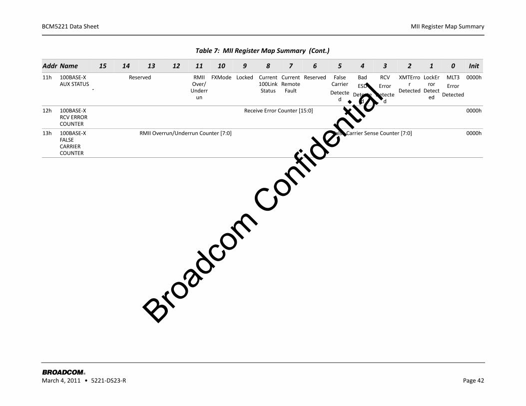
Broadc
om C
onfid
entia
l
BROADCOM March 4, 2011 • 5221-DS23-R Page 42
®
MII Register Map SummaryBCM5221 Data Sheet
11h 100BASE-X AUX STATUS
-
Reserved RMII Over/
Underrun
FXMode Locked Current 100Link Status
Current Remote
Fault
Reserved False Carrier
Detected
Bad
ESD
Detected
RCV
Error
Detected
XMTError
Detected
LockError
Detected
MLT3
Error
Detected
0000h
12h 100BASE-X RCV ERROR COUNTER
Receive Error Counter [15:0] 0000h
13h 100BASE-X FALSE CARRIER COUNTER
RMII Overrun/Underrun Counter [7:0] False Carrier Sense Counter [7:0] 0000h
Table 7: MII Register Map Summary (Cont.)
Addr Name 15 14 13 12 11 10 9 8 7 6 5 4 3 2 1 0 Init
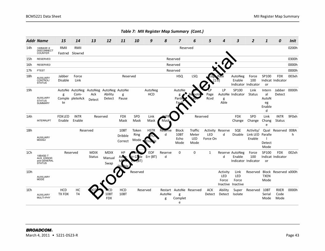
Broadc
om C
onfid
entia
l
BROADCOM March 4, 2011 • 5221-DS23-R Page 43
®
MII Register Map SummaryBCM5221 Data Sheet
14h 100BASE-X DISCONNECT COUNTER
RMII
Fastrxd
RMII
Slowrxd
Reserved 0200h
15h RESERVED Reserved 0300h
16h RESERVED Reserved 0000h
17h PTEST Reserved 0000h
18hAUXILIARY CONTROL/STATUS
JabberDisable
Force Link
Reserved HSQ LSQ Edge Rate[1:0]
AutoNegEnable
Indicator
Force 100
Indicator
SP100Indicat
or
FDXIndicator
003xh
19h
AUXILIARYSTATUS SUMMARY
AutoNeg
Complete
AutoNegCom-
pleteAck
AutoNegAck
Detect
AutoNegAbilityDetect
AutoNeg
Pause
AutoNegHCD
AutoNeg
PardetFault
LPRemote
Fault
LPPageRcvd
LPAutoNe
gAble
SP100Indicator
LinkStatus
Internal
AutoNeg
Enabled
JabberDetect
0000h
1AhINTERRUPT
FDX LED Enable
INTR Enable
Reserved FDX Mask
SPD Mask
Link Mask
INTR Mask
Reserved FDX Change
SPD Change
Link Chang
e
INTRStatus
9F0xh
1Bh
AUXILIARY MODE2
Reserved 10BT
Dribble
Correct
Token Ring
Mode
HSTR
FIFO
Enable
Reserved
Block10BTEcho
Mode
TrafficMeter
LEDMode
ActivityLED
Force On
Reserved
SQE Disable
Activity/Link LEDEnable
QualParalle
lDetectMode
Reserved 008Ah
1Ch10BASE-T AUX. ERROR and GENERAL STATUS
Reserved MDIX Status
MDIX
Manual
Swap
HP Auto-MDIX
Disable
Manchstr CodeErr (BT)
EOFErr (BT)
Reserved
0 0 1 Reserved
AutoNegEnable
Indicator
Force 100
Indicator
SP100Indicat
or
FDXIndicator
002xh
1DhAUXILIARY MODE
Reserved ActivityLED
ForceInactive
LinkLED
ForceInactive
Reserved Block TXENMode
Reserved x000h
1EhAUXILIARY MULTI-PHY
HCDTX FDX
HCT4
HCDTX
HCD 10BT FDX
HCD 10BT
Reserved Restart AutoNe
g
AutoNeg
Complete
Reserved ACK Detect
Ability Detect
Super Isolate
Reserved 10BT Serial Mode
RXER Code Mode
0000h
Table 7: MII Register Map Summary (Cont.)
Addr Name 15 14 13 12 11 10 9 8 7 6 5 4 3 2 1 0 Init
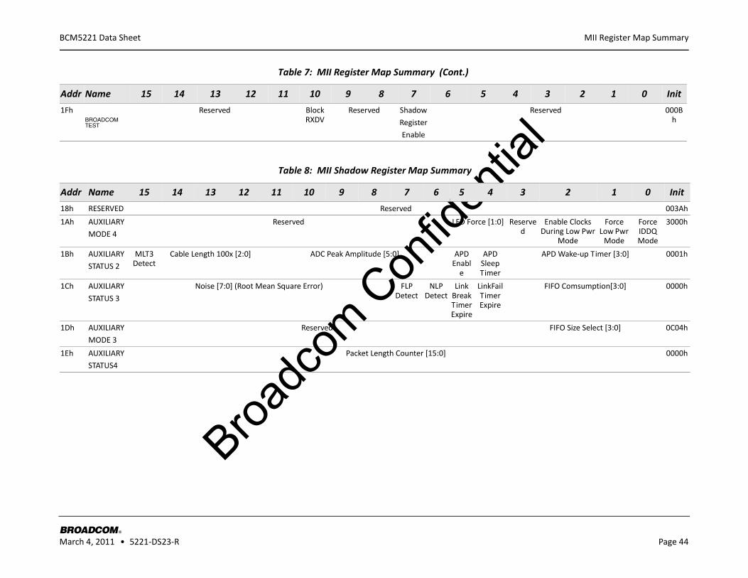
Broadc
om C
onfid
entia
l
BROADCOM March 4, 2011 • 5221-DS23-R Page 44
®
MII Register Map SummaryBCM5221 Data Sheet
1FhBROADCOM TEST
Reserved Block RXDV
Reserved Shadow
Register
Enable
Reserved 000Bh
Table 8: MII Shadow Register Map Summary
Addr Name 15 14 13 12 11 10 9 8 7 6 5 4 3 2 1 0 Init
18h RESERVED Reserved 003Ah
1Ah AUXILIARY
MODE 4
Reserved LED Force [1:0] Reserved
Enable ClocksDuring Low Pwr
Mode
Force Low Pwr
Mode
Force IDDQ Mode
3000h
1Bh AUXILIARY
STATUS 2
MLT3 Detect
Cable Length 100x [2:0] ADC Peak Amplitude [5:0] APD Enabl
e
APD Sleep Timer
APD Wake-up Timer [3:0] 0001h
1Ch AUXILIARY
STATUS 3
Noise [7:0] (Root Mean Square Error) FLP Detect
NLPDetect
LinkBreakTimerExpire
LinkFail Timer Expire
FIFO Comsumption[3:0] 0000h
1Dh AUXILIARY
MODE 3
Reserved FIFO Size Select [3:0] 0C04h
1Eh AUXILIARY
STATUS4
Packet Length Counter [15:0] 0000h
Table 7: MII Register Map Summary (Cont.)
Addr Name 15 14 13 12 11 10 9 8 7 6 5 4 3 2 1 0 Init
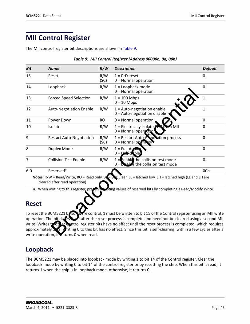
Broadc
om C
onfid
entia
l
MII Control Register
BROADCOM March 4, 2011 • 5221-DS23-R Page 45
®
BCM5221 Data Sheet
MII Control RegisterThe MII control register bit descriptions are shown in Table 9.
ResetTo reset the BCM5221 by software control, 1 must be written to bit 15 of the Control register using an MII write operation. The bit clears itself after the reset process is complete and need not be cleared using a second MII write. Writes to other Control register bits have no effect until the reset process is completed, which requires approximately 1 μs. Writing 0 to this bit has no effect. Since this bit is self-clearing, within a few cycles after a write operation, it returns 0 when read.
LoopbackThe BCM5221 may be placed into loopback mode by writing 1 to bit 14 of the Control register. Clear the loopback mode by writing 0 to bit 14 of the control register or by resetting the chip. When this bit is read, it returns 1 when the chip is in loopback mode, otherwise, it returns 0.
Table 9: MII Control Register (Address 00000b, 0d, 00h)
Bit Name R/W Description Default
15 Reset R/W (SC)
1 = PHY reset 0 = Normal operation
0
14 Loopback R/W 1 = Loopback mode 0 = Normal operation
0
13 Forced Speed Selection R/W 1 = 100 Mbps 0 = 10 Mbps
1
12 Auto-Negotiation Enable R/W 1 = Auto-negotiation enable 0 = Auto-negotiation disable
1
11 Power Down RO 0 = Normal operation 0
10 Isolate R/W 1 = Electrically isolate PHY from MII 0 = Normal operation
0
9 Restart Auto-Negotiation R/W (SC)
1 = Restart Auto-negotiation process 0 = Normal operation
0
8 Duplex Mode R/W 1 = Full-duplex 0 = Half-duplex
0
7 Collision Test Enable R/W 1 = Enable the collision test mode 0 = Disable the collision test mode
0
6:0 Reserveda
a. When writing to this register, preserve existing values of reserved bits by completing a Read/Modify Write.
– – 00hNotes: R/W = Read/Write, RO = Read only, SC = Self Clear, LL = latched low, LH = latched high (LL and LH are
cleared after read operation)
Broadc
om C
onfid
entia
l
MII Control Register
BROADCOM March 4, 2011 • 5221-DS23-R Page 46
®
BCM5221 Data Sheet
Forced Speed SelectionIf auto-negotiation is enabled (both auto-negotiation pin and bit are enabled) or disabled by hardware control (auto-negotiation pin is pulled low), this bit has no effect on the speed selection. However, if auto-negotiation is disabled by software control, the operating speed of the BCM5221 can be forced by writing the appropriate value to bit 13 of the Control register. Writing 1 to this bit forces 100BASE-X operation, while writing 0 forces 10BASE-T operation. When this bit is read, it returns the value of the software-controlled forced speed selection only. To read the overall state of forced speed selection, including both hardware and software control, use bit 2 of the Auxiliary Control register (18h).
Auto-Negotiation EnableAuto-negotiation can be disabled by one of two methods: hardware or software control. If the ANEN input pin is driven to a logic 0, auto-negotiation is disabled by hardware control. If bit 12 of the Control register is written with a value of 0, auto-negotiation is disabled by software control. When auto-negotiation is disabled in this manner, writing 1 to the same bit of the Control register or resetting the chip reenables auto-negotiation. Writing to this bit has no effect when auto-negotiation has been disabled by hardware control. When read, this bit returns the value most recently written to this location, or 1 if it has not been written since the last chip reset.
Power DownThe power modes of the BCM5221 are not accessible by this MII register bit. Use LOWPWR pin control instead.
IsolateThe PHY can be isolated from its Media Independent Interface by writing 1 to bit 10 of the Control register. All MII outputs are tristated and all MII inputs are ignored. Because the MII management interface is still active, the isolate mode can be cleared by writing 0 to bit 10 of the control register or by resetting the chip. When this bit is read, it returns 1 when the chip is in isolate mode; otherwise, it returns 0.
Restart Auto-NegotiationBit 9 of the Control register is a self-clearing bit that allows the auto-negotiation process to be restarted, regardless of the current status of the auto-negotiation state machine. For this bit to have an effect, auto-negotiation must be enabled. Writing 1 to this bit restarts the auto-negotiation, while writing 0 to this bit has no effect. Because the bit is self-clearing after only a few cycles, it always returns 0 when read. The operation of this bit is identical to bit 8 of the Auxiliary Multiple PHY register (1Eh).
Duplex ModeBy default, the BCM5221 powers up in half-duplex mode. The chip can be forced into full-duplex mode by writing 1 to bit 8 of the Control register while auto-negotiation is disabled. Half-duplex mode can be resumed by writing 0 to bit 8 of the Control register or by resetting the chip.

Broadc
om C
onfid
entia
l
MII Control Register
BROADCOM March 4, 2011 • 5221-DS23-R Page 47
®
BCM5221 Data Sheet
Collision TestTest the COL pin by activating the collision test mode. While in this mode, asserting TXEN causes the COL output to go high within 512 bit times. Deasserting TXEN causes the COL output to go low within 4 bit times. Writing 1 to bit 7 of the Control register enables the collision test mode. Writing 0 to this bit or resetting the chip disables the collision test mode. When this bit is read, it returns 1 when the collision test mode has been enabled; otherwise, it returns 0. This bit should only be set while in loopback test mode.
Reserved BitsAll reserved MII register bits must be written as 0 at all times. Ignore the BCM5221 output when these bits are read.
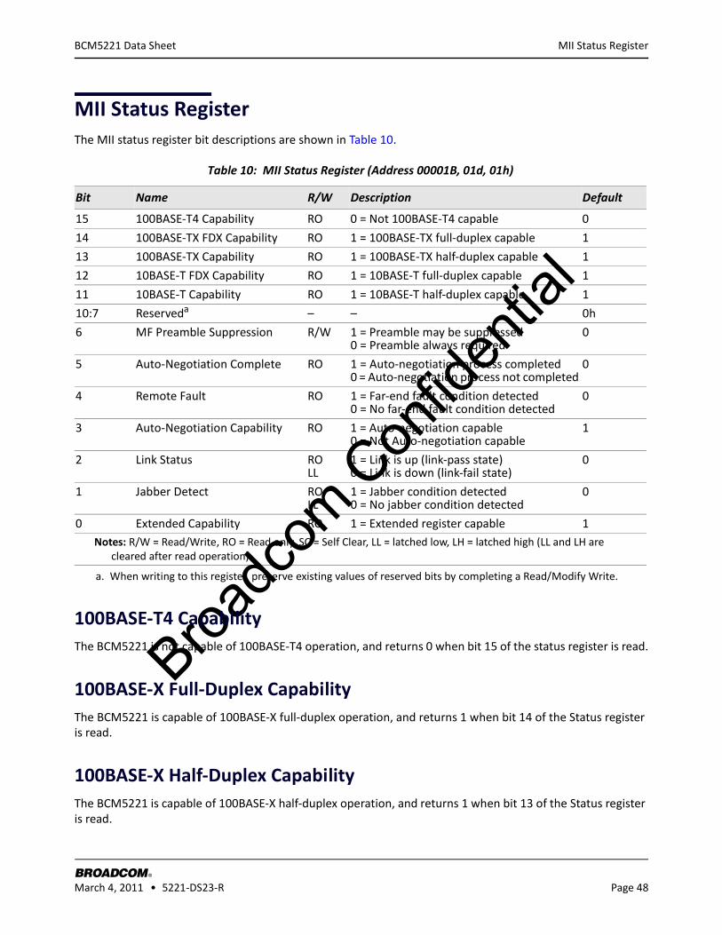
Broadc
om C
onfid
entia
l
MII Status Register
BROADCOM March 4, 2011 • 5221-DS23-R Page 48
®
BCM5221 Data Sheet
MII Status RegisterThe MII status register bit descriptions are shown in Table 10.
100BASE-T4 CapabilityThe BCM5221 is not capable of 100BASE-T4 operation, and returns 0 when bit 15 of the status register is read.
100BASE-X Full-Duplex CapabilityThe BCM5221 is capable of 100BASE-X full-duplex operation, and returns 1 when bit 14 of the Status register is read.
100BASE-X Half-Duplex CapabilityThe BCM5221 is capable of 100BASE-X half-duplex operation, and returns 1 when bit 13 of the Status register is read.
Table 10: MII Status Register (Address 00001B, 01d, 01h)
Bit Name R/W Description Default
15 100BASE-T4 Capability RO 0 = Not 100BASE-T4 capable 0
14 100BASE-TX FDX Capability RO 1 = 100BASE-TX full-duplex capable 1
13 100BASE-TX Capability RO 1 = 100BASE-TX half-duplex capable 1
12 10BASE-T FDX Capability RO 1 = 10BASE-T full-duplex capable 1
11 10BASE-T Capability RO 1 = 10BASE-T half-duplex capable 1
10:7 Reserveda
a. When writing to this register, preserve existing values of reserved bits by completing a Read/Modify Write.
– – 0h
6 MF Preamble Suppression R/W 1 = Preamble may be suppressed 0 = Preamble always required
0
5 Auto-Negotiation Complete RO 1 = Auto-negotiation process completed 0 = Auto-negotiation process not completed
0
4 Remote Fault RO 1 = Far-end fault condition detected 0 = No far-end fault condition detected
0
3 Auto-Negotiation Capability RO 1 = Auto-negotiation capable 0 = Not Auto-negotiation capable
1
2 Link Status RO LL
1 = Link is up (link-pass state) 0 = Link is down (link-fail state)
0
1 Jabber Detect RO LL
1 = Jabber condition detected 0 = No jabber condition detected
0
0 Extended Capability RO 1 = Extended register capable 1Notes: R/W = Read/Write, RO = Read only, SC = Self Clear, LL = latched low, LH = latched high (LL and LH are
cleared after read operation)
Broadc
om C
onfid
entia
l
MII Status Register
BROADCOM March 4, 2011 • 5221-DS23-R Page 49
®
BCM5221 Data Sheet
10BASE-T Full-Duplex CapabilityThe BCM5221 is capable of 10BASE-T full-duplex operation, and returns 1 when bit 12 of the Status register is read.
10BASE-T Half-Duplex CapabilityThe BCM5221 is capable of 10BASE-T half-duplex operation and returns 1 when bit 11 of the Status register is read.
Reserved BitsIgnore the BCM5221 output when these bits are read.
Preamble SuppressionThis bit is the only writable bit in the Status register. Setting this bit to 1 allows subsequent MII management frames to be accepted with or without the standard preamble pattern. When preamble suppression is enabled, only 2 preamble bits are required between successive management commands, instead of the normal 32.
Auto-Negotiation CompleteReturns 1 if auto-negotiation process has been completed and the contents of registers 4, 5, and 6 are valid.
Remote FaultThe PHY returns 1 on bit 4 of the status register when its link partner has signalled a far-end fault condition. When a far-end fault occurs, the bit is latched at 1 and remains so until the register is read and the remote fault condition has been cleared.
Auto-Negotiation CapabilityThe BCM5221 is capable of performing IEEE auto-negotiation, and returns 1 when bit 4 of the Status register is read, regardless of whether the auto-negotiation function has been disabled.
Link StatusThe BCM5221 returns 1 on bit 2 of the Status register when the link-state machine is in link-pass, indicating that a valid link has been established. Otherwise, it returns 0. When a link failure occurs after the link-pass state has been entered, the link status bit is etched at 0 and remains so until the bit is read. After the bit is read, it becomes 1 when the link-pass state is entered again.
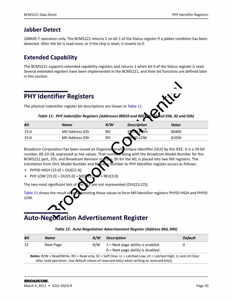
Broadc
om C
onfid
entia
l
PHY Identifier Registers
BROADCOM March 4, 2011 • 5221-DS23-R Page 50
®
BCM5221 Data Sheet
Jabber Detect10BASE-T operation only. The BCM5221 returns 1 on bit 1 of the Status register if a jabber condition has been detected. After the bit is read once, or if the chip is reset, it reverts to 0.
Extended CapabilityThe BCM5221 supports extended capability registers and returns 1 when bit 0 of the Status register is read. Several extended registers have been implemented in the BCM5221, and their bit functions are defined later in this section.
PHY Identifier RegistersThe physical indentifier register bit descriptions are shown in Table 11.
Broadcom Corporation has been issued an Organizationally Unique Identifier (OUI) by the IEEE. It is a 24-bit number, 00-10-18, expressed as hex values. That number, along with the Broadcom Model Number for the BCM5221 part, 1Eh, and Broadcom Revision number, 0h for the A0, is placed into two MII registers. The translation from OUI, Model Number and Revision Number to PHY Identifier register occurs as follows:
• PHYID HIGH [15:0] = OUI[21:6]
• PHY LOW [15:0] = OUI[5:0] + MODEL[5:0] + REV[3:0]
The two most significant bits of the OUI are not represented (OUI[23:22]).
Table 11 shows the result of concatenating these values to form MII Identifier registers PHYID HIGH and PHYID LOW.
Auto-Negotiation Advertisement Register
Table 11: PHY Indentifier Registers (Addresses 00010 and 00011b, 02 and 03b, 02 and 03h)
Bit Name R/W Description Value
15:0 MII Address 02h RO PHYID HIGH 0040h
15:0 MII Address 03h RO PHYID LOW 61E0h
Table 12: Auto-Negotiation Advertisement Register (Address 04d, 04h)
Bit Name R/W Description Default
15 Next Page R/W 1 = Next page ability is enabled.0 = Next page ability is disabled.
0
Notes: R/W = Read/Write, RO = Read only, SC = Self Clear, LL = Latched Low, LH = Latched High, LL and LH Clear after read operation. Use default values of reserved bit(s) when writing to reserved bit(s).
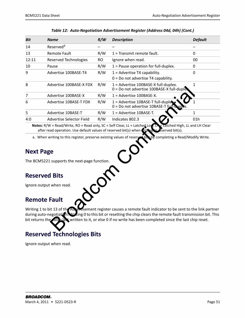
Broadc
om C
onfid
entia
l
Auto-Negotiation Advertisement Register
BROADCOM March 4, 2011 • 5221-DS23-R Page 51
®
BCM5221 Data Sheet
Next PageThe BCM5221 supports the next-page function.
Reserved BitsIgnore output when read.
Remote FaultWriting 1 to bit 13 of the Advertisement register causes a remote fault indicator to be sent to the link partner during auto-negotiation. Writing 0 to this bit or resetting the chip clears the remote fault transmission bit. This bit returns the value last written to it, or else 0 if no write has been completed since the last chip reset.
Reserved Technologies BitsIgnore output when read.
14 Reserveda – – –
13 Remote Fault R/W 1 = Transmit remote fault. 0
12:11 Reserved Technologies RO Ignore when read. 00
10 Pause R/W 1 = Pause operation for full-duplex. 0
9 Advertise 100BASE-T4 R/W 1 = Advertise T4 capability.0 = Do not advertise T4 capability.
0
8 Advertise 100BASE-X FDX R/W 1 = Advertise 100BASE-X full-duplex. 0 = Do not advertise 100BASE-X full-duplex.
1
7 Advertise 100BASE-X R/W 1 = Advertise 100BASE-X. 1
6 Advertise 10BASE-T FDX R/W 1 = Advertise 10BASE-T full-duplex. 0 = Do not advertise 10BASE-T full-duplex.
1
5 Advertise 10BASE-T R/W 1 = Advertise 10BASE-T. 1
4:0 Advertise Selector Field R/W Indicates 802.3 01h
a. When writing to this register, preserve existing values of reserved bits by completing a Read/Modify Write.
Table 12: Auto-Negotiation Advertisement Register (Address 04d, 04h) (Cont.)
Bit Name R/W Description Default
Notes: R/W = Read/Write, RO = Read only, SC = Self Clear, LL = Latched Low, LH = Latched High, LL and LH Clear after read operation. Use default values of reserved bit(s) when writing to reserved bit(s).
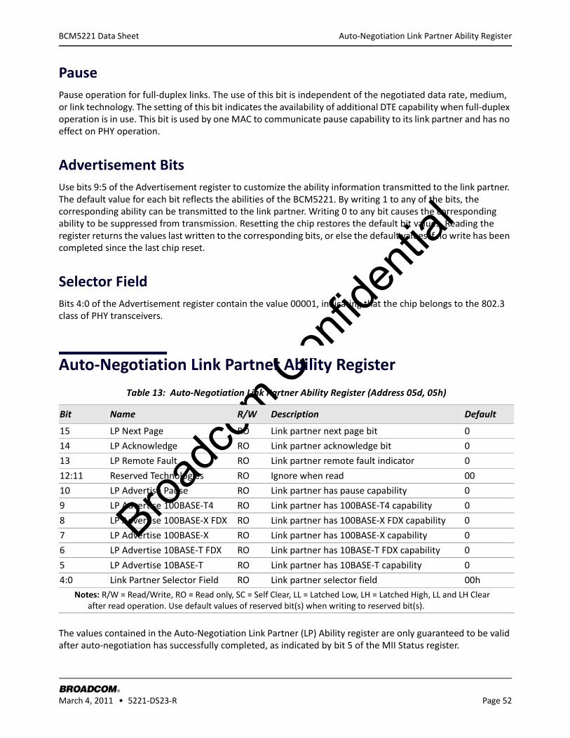
Broadc
om C
onfid
entia
l
Auto-Negotiation Link Partner Ability Register
BROADCOM March 4, 2011 • 5221-DS23-R Page 52
®
BCM5221 Data Sheet
PausePause operation for full-duplex links. The use of this bit is independent of the negotiated data rate, medium, or link technology. The setting of this bit indicates the availability of additional DTE capability when full-duplex operation is in use. This bit is used by one MAC to communicate pause capability to its link partner and has no effect on PHY operation.
Advertisement BitsUse bits 9:5 of the Advertisement register to customize the ability information transmitted to the link partner. The default value for each bit reflects the abilities of the BCM5221. By writing 1 to any of the bits, the corresponding ability can be transmitted to the link partner. Writing 0 to any bit causes the corresponding ability to be suppressed from transmission. Resetting the chip restores the default bit values. Reading the register returns the values last written to the corresponding bits, or else the default values if no write has been completed since the last chip reset.
Selector FieldBits 4:0 of the Advertisement register contain the value 00001, indicating that the chip belongs to the 802.3 class of PHY transceivers.
Auto-Negotiation Link Partner Ability Register
The values contained in the Auto-Negotiation Link Partner (LP) Ability register are only guaranteed to be valid after auto-negotiation has successfully completed, as indicated by bit 5 of the MII Status register.
Table 13: Auto-Negotiation Link Partner Ability Register (Address 05d, 05h)
Bit Name R/W Description Default
15 LP Next Page RO Link partner next page bit 0
14 LP Acknowledge RO Link partner acknowledge bit 0
13 LP Remote Fault RO Link partner remote fault indicator 0
12:11 Reserved Technologies RO Ignore when read 00
10 LP Advertise Pause RO Link partner has pause capability 0
9 LP Advertise 100BASE-T4 RO Link partner has 100BASE-T4 capability 0
8 LP Advertise 100BASE-X FDX RO Link partner has 100BASE-X FDX capability 0
7 LP Advertise 100BASE-X RO Link partner has 100BASE-X capability 0
6 LP Advertise 10BASE-T FDX RO Link partner has 10BASE-T FDX capability 0
5 LP Advertise 10BASE-T RO Link partner has 10BASE-T capability 0
4:0 Link Partner Selector Field RO Link partner selector field 00hNotes: R/W = Read/Write, RO = Read only, SC = Self Clear, LL = Latched Low, LH = Latched High, LL and LH Clear
after read operation. Use default values of reserved bit(s) when writing to reserved bit(s).
Broadc
om C
onfid
entia
l
Auto-Negotiation Expansion Register
BROADCOM March 4, 2011 • 5221-DS23-R Page 53
®
BCM5221 Data Sheet
LP Next PageBit 15 of the Link Partner Ability register returns a value of 1 when the link partner implements the next page function and has next page information that it wants to transmit. The BCM5221 does not implement the next page function, and thus ignores the next page bit, except to copy it to this register.
LP AcknowledgeBit 14 of the Link Partner Ability register is used by auto-negotiation to indicate that a device has successfully received its link partner’s link code word.
LP Remote FaultBit 13 of the Link Partner Ability register returns a value of 1 when the link partner signals that a remote fault has occurred. The BCM5221 simply copies the value to this register and does not act upon it.
Reserved BitsIgnore when read.
LP Advertise PauseIndicates that the Link Partner Pause bit is set.
LP Advertise BitsBits 9:5 of the Link Partner Ability register reflect the abilities of the link partner. A 1 on any of these bits indicates that the link partner is capable of performing the corresponding mode of operation. Bits 9:5 are cleared any time auto-negotiation is restarted or the BCM5221 is reset.
LP Selector FieldBits 4:0 of the Link Partner Ability register reflect the value of the link partner’s selector field. These bits are cleared any time auto-negotiation is restarted or the chip is reset.
Auto-Negotiation Expansion RegisterTable 14 shows the Auto-Negotiation Expansion register bit descriptions.
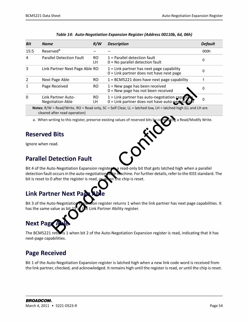
Broadc
om C
onfid
entia
l
Auto-Negotiation Expansion Register
BROADCOM March 4, 2011 • 5221-DS23-R Page 54
®
BCM5221 Data Sheet
Reserved BitsIgnore when read.
Parallel Detection FaultBit 4 of the Auto-Negotiation Expansion register is a read-only bit that gets latched high when a parallel detection fault occurs in the auto-negotiation state machine. For further details, refer to the IEEE standard. The bit is reset to 0 after the register is read, or when the chip is reset.
Link Partner Next Page AbleBit 3 of the Auto-Negotiation Expansion register returns 1 when the link partner has next page capabilities. It has the same value as bit 15 of the Link Partner Ability register.
Next Page AbleThe BCM5221 returns 1 when bit 2 of the Auto-Negotiation Expansion register is read, indicating that it has next-page capabilities.
Page ReceivedBit 1 of the Auto-Negotiation Expansion register is latched high when a new link code word is received from the link partner, checked, and acknowledged. It remains high until the register is read, or until the chip is reset.
Table 14: Auto-Negotiation Expansion Register (Address 00110b, 6d, 06h)
Bit Name R/W Description Default
15:5 Reserveda
a. When writing to this register, preserve existing values of reserved bits by completing a Read/Modify Write.
– – 000h
4 Parallel Detection Fault RO LH
1 = Parallel detection fault 0 = No parallel detection fault 0
3 Link Partner Next Page Able RO 1 = Link partner has next page capability 0 = Link partner does not have next page 0
2 Next Page Able RO 1 = BCM5221 does have next page capability 1
1 Page Received RO 1 = New page has been received 0 = New page has not been received 0
0 Link Partner Auto-Negotiation Able
RO LH
1 = Link partner has auto-negotiation capability 0 = Link partner does not have auto-negotiation 0
Notes: R/W = Read/Write, RO = Read only, SC = Self Clear, LL = latched low, LH = latched high (LL and LH are cleared after read operation)
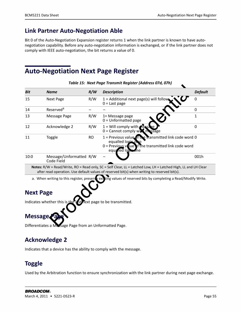
Broadc
om C
onfid
entia
l
Auto-Negotiation Next Page Register
BROADCOM March 4, 2011 • 5221-DS23-R Page 55
®
BCM5221 Data Sheet
Link Partner Auto-Negotiation AbleBit 0 of the Auto-Negotiation Expansion register returns 1 when the link partner is known to have auto-negotiation capability. Before any auto-negotiation information is exchanged, or if the link partner does not comply with IEEE auto-negotiation, the bit returns a value of 0.
Auto-Negotiation Next Page Register
Next PageIndicates whether this is the last next page to be transmitted.
Message PageDifferentiates a Message Page from an Unformatted Page.
Acknowledge 2Indicates that a device has the ability to comply with the message.
ToggleUsed by the Arbitration function to ensure synchronization with the link partner during next page exchange.
Table 15: Next Page Transmit Register (Address 07d, 07h)
Bit Name R/W Description Default
15 Next Page R/W 1 = Additional next page(s) will follow 0 = Last page
0
14 Reserveda
a. When writing to this register, preserve existing values of reserved bits by completing a Read/Modify Write.
– – 0
13 Message Page R/W 1= Message page 0 = Unformatted page
1
12 Acknowledge 2 R/W 1 = Will comply with message 0 = Cannot comply with message
0
11 Toggle RO 1 = Previous value of the transmitted link code word equalled logic zero 0 = Previous value of the transmitted link code word equalled logic one
0
10:0 Message/Unformatted Code Field
R/W – 001h
Notes: R/W = Read/Write, RO = Read only, SC = Self Clear, LL = Latched Low, LH = Latched High, LL and LH Clear after read operation. Use default values of reserved bit(s) when writing to reserved bit(s).

Broadc
om C
onfid
entia
l
Auto-Negotiation Next Page Register
BROADCOM March 4, 2011 • 5221-DS23-R Page 56
®
BCM5221 Data Sheet
Message Code FieldAn 11-bit-wide field, encoding 2048 possible messages.
Unformatted Code FieldAn 11-bit-wide field, which may contain an arbitrary value.
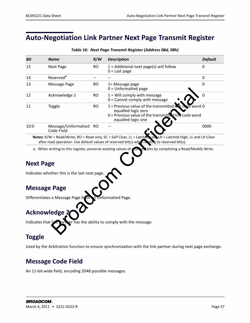
Broadc
om C
onfid
entia
l
Auto-Negotiation Link Partner Next Page Transmit Register
BROADCOM March 4, 2011 • 5221-DS23-R Page 57
®
BCM5221 Data Sheet
Auto-Negotiation Link Partner Next Page Transmit Register
Next PageIndicates whether this is the last next page.
Message PageDifferentiates a Message Page from an Unformatted Page.
Acknowledge 2Indicates that link partner has the ability to comply with the message.
ToggleUsed by the Arbitration function to ensure synchronization with the link partner during next page exchange.
Message Code FieldAn 11-bit-wide field, encoding 2048 possible messages.
Table 16: Next Page Transmit Register (Address 08d, 08h)
Bit Name R/W Description Default
15 Next Page RO 1 = Additional next page(s) will follow 0 = Last page
0
14 Reserveda
a. When writing to this register, preserve existing values of reserved bits by completing a Read/Modify Write.
– – 0
13 Message Page RO 1= Message page 0 = Unformatted page
0
12 Acknowledge 2 RO 1 = Will comply with message 0 = Cannot comply with message
0
11 Toggle RO 1 = Previous value of the transmitted link code word equalled logic zero 0 = Previous value of the transmitted link code word equalled logic one
0
10:0 Message/Unformatted Code Field
RO – 000h
Notes: R/W = Read/Write, RO = Read only, SC = Self Clear, LL = Latched Low, LH = Latched High, LL and LH Clear after read operation. Use default values of reserved bit(s) when writing to reserved bit(s).

Broadc
om C
onfid
entia
l
Auto-Negotiation Link Partner Next Page Transmit Register
BROADCOM March 4, 2011 • 5221-DS23-R Page 58
®
BCM5221 Data Sheet
Unformatted Code FieldAn 11-bit-wide field, which may contain an arbitrary value.
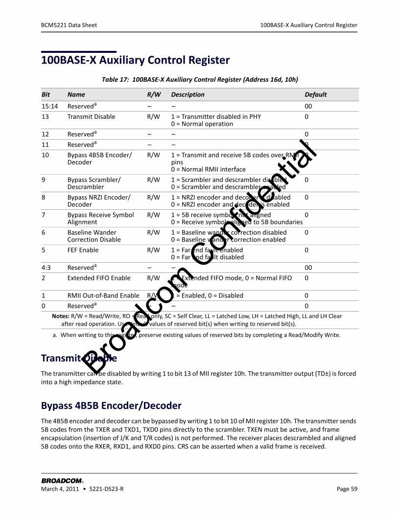
Broadc
om C
onfid
entia
l
100BASE-X Auxiliary Control Register
BROADCOM March 4, 2011 • 5221-DS23-R Page 59
®
BCM5221 Data Sheet
100BASE-X Auxiliary Control Register
Transmit DisableThe transmitter can be disabled by writing 1 to bit 13 of MII register 10h. The transmitter output (TD±) is forced into a high impedance state.
Bypass 4B5B Encoder/DecoderThe 4B5B encoder and decoder can be bypassed by writing 1 to bit 10 of MII register 10h. The transmitter sends 5B codes from the TXER and TXD1, TXD0 pins directly to the scrambler. TXEN must be active, and frame encapsulation (insertion of J/K and T/R codes) is not performed. The receiver places descrambled and aligned 5B codes onto the RXER, RXD1, and RXD0 pins. CRS can be asserted when a valid frame is received.
Table 17: 100BASE-X Auxiliary Control Register (Address 16d, 10h)
Bit Name R/W Description Default
15:14 Reserveda
a. When writing to this register, preserve existing values of reserved bits by completing a Read/Modify Write.
– – 00
13 Transmit Disable R/W 1 = Transmitter disabled in PHY 0 = Normal operation
0
12 Reserveda – – 0
11 Reserveda – – 0
10 Bypass 4B5B Encoder/Decoder
R/W 1 = Transmit and receive 5B codes over RMII pins 0 = Normal RMII interface
0
9 Bypass Scrambler/Descrambler
R/W 1 = Scrambler and descrambler disabled 0 = Scrambler and descrambler enabled
0
8 Bypass NRZI Encoder/Decoder
R/W 1 = NRZI encoder and decoder is disabled 0 = NRZI encoder and decoder is enabled
0
7 Bypass Receive Symbol Alignment
R/W 1 = 5B receive symbols not aligned 0 = Receive symbols aligned to 5B boundaries
0
6 Baseline Wander Correction Disable
R/W 1 = Baseline wander correction disabled 0 = Baseline wander correction enabled
0
5 FEF Enable R/W 1 = Far end fault enabled 0 = Far end fault disabled
0
4:3 Reserveda – – 00
2 Extended FIFO Enable R/W 1 = Extended FIFO mode, 0 = Normal FIFO mode
0
1 RMII Out-of-Band Enable R/W 1 = Enabled, 0 = Disabled 0
0 Reserveda – – 0 Notes: R/W = Read/Write, RO = Read only, SC = Self Clear, LL = Latched Low, LH = Latched High, LL and LH Clear
after read operation. Use default values of reserved bit(s) when writing to reserved bit(s).
Broadc
om C
onfid
entia
l
100BASE-X Auxiliary Control Register
BROADCOM March 4, 2011 • 5221-DS23-R Page 60
®
BCM5221 Data Sheet
Bypass Scrambler/DescramblerThe stream cipher function can be disabled by writing 1 to bit 9 of MII register 10h. The stream cipher function is reenabled by writing 0 to this bit.
Bypass NRZI Encoder/DecoderThe NRZI encoder and decoder can be bypassed by writing 1 to bit 8 of MII register 10h, causing 3-level NRZ data to be transmitted and received on the cable. Normal operation (3-level NRZI encoding and decoding) can be reenabled by writing 0 to this bit.
Bypass Receive Symbol AlignmentReceive symbol alignment can be bypassed by writing 1 to bit 7 of MII register 10h. When used in conjunction with the bypass 4B5B encoder/decoder bit, unaligned 5B codes are placed directly on the RXER and RXD1, RXD0 pins.
Baseline Wander Correction DisableThe baseline wander correction circuit can be disabled by writing 1 to bit 6 of MII register 10h. The BCM5221 corrects for baseline wander on the receive data signal when this bit is cleared.
FEF EnableControls the far end fault mechanism associated with 100BASE-FX operation. A 1 enables the FEF function and 0 disables it.
Extended RMII FIFO EnableControls the extended RMII FIFO mechanism.
RMII Out-of-Band EnableControls the RMII out-of band mechanism within the RMII receive logic.
Reserved BitsThe reserved bits of the 100BASE-X Auxiliary Control register must be written as 0 at all times. Ignore the BCM5221 outputs when these bits are read.
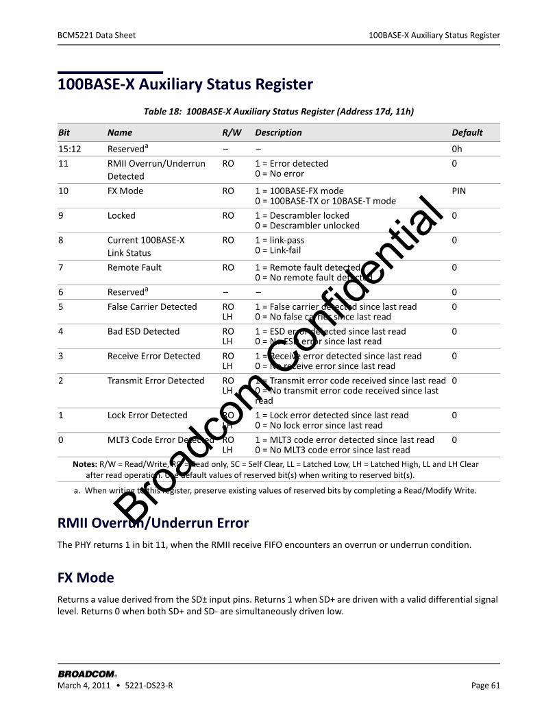
Broadc
om C
onfid
entia
l
100BASE-X Auxiliary Status Register
BROADCOM March 4, 2011 • 5221-DS23-R Page 61
®
BCM5221 Data Sheet
100BASE-X Auxiliary Status Register
RMII Overrun/Underrun ErrorThe PHY returns 1 in bit 11, when the RMII receive FIFO encounters an overrun or underrun condition.
FX ModeReturns a value derived from the SD± input pins. Returns 1 when SD+ are driven with a valid differential signal level. Returns 0 when both SD+ and SD- are simultaneously driven low.
Table 18: 100BASE-X Auxiliary Status Register (Address 17d, 11h)
Bit Name R/W Description Default
15:12 Reserveda
a. When writing to this register, preserve existing values of reserved bits by completing a Read/Modify Write.
– – 0h
11 RMII Overrun/UnderrunDetected
RO 1 = Error detected 0 = No error
0
10 FX Mode RO 1 = 100BASE-FX mode 0 = 100BASE-TX or 10BASE-T mode
PIN
9 Locked RO 1 = Descrambler locked 0 = Descrambler unlocked
0
8 Current 100BASE-X Link Status
RO 1 = link-pass 0 = Link-fail
0
7 Remote Fault RO 1 = Remote fault detected 0 = No remote fault detected
0
6 Reserveda – – 0
5 False Carrier Detected RO LH
1 = False carrier detected since last read 0 = No false carrier since last read
0
4 Bad ESD Detected RO LH
1 = ESD error detected since last read 0 = No ESD error since last read
0
3 Receive Error Detected RO LH
1 = Receive error detected since last read 0 = No receive error since last read
0
2 Transmit Error Detected RO LH
1 = Transmit error code received since last read 0 = No transmit error code received since last read
0
1 Lock Error Detected RO LH
1 = Lock error detected since last read 0 = No lock error since last read
0
0 MLT3 Code Error Detected RO LH
1 = MLT3 code error detected since last read 0 = No MLT3 code error since last read
0
Notes: R/W = Read/Write, RO = Read only, SC = Self Clear, LL = Latched Low, LH = Latched High, LL and LH Clear after read operation. Use default values of reserved bit(s) when writing to reserved bit(s).
Broadc
om C
onfid
entia
l
100BASE-X Auxiliary Status Register
BROADCOM March 4, 2011 • 5221-DS23-R Page 62
®
BCM5221 Data Sheet
LockedThe PHY returns 1 in bit 9 when the descrambler is locked to the incoming data stream. Otherwise, it returns 0.
Current 100BASE-X Link StatusThe PHY returns 1 in bit 8 when the 100BASE-X link status is good. Otherwise, it returns 0.
Remote FaultThe PHY returns 1 while its link partner is signalling a far-end fault condition. Otherwise it returns 0.
False Carrier DetectedThe PHY returns 1 in bit 5 of the Extended Status register if a false carrier has been detected since the last time this register was read. Otherwise it returns 0.
Bad ESD DetectedThe PHY returns 1 in bit 4 if an end of stream delimiter error has been detected since the last time this register was read. Otherwise it returns 0.
Receive Error DetectedThe PHY returns 1 in bit 3 if a packet was received with an invalid code since the last time this register was read. Otherwise it returns 0.
Transmit Error DetectedThe PHY returns 1 in bit 2 if a packet was received with a transmit error code since the last time this register was read. Otherwise it returns 0.
Lock Error DetectedThe PHY returns 1 in bit 1 if the descrambler has lost lock since the last time this register was read. Otherwise it returns 0.
MLT3 Code Error DetectedThe PHY returns 1 in bit 0 if an MLT3 coding error has been detected in the receive data stream since the last time this register was read. Otherwise it returns 0.
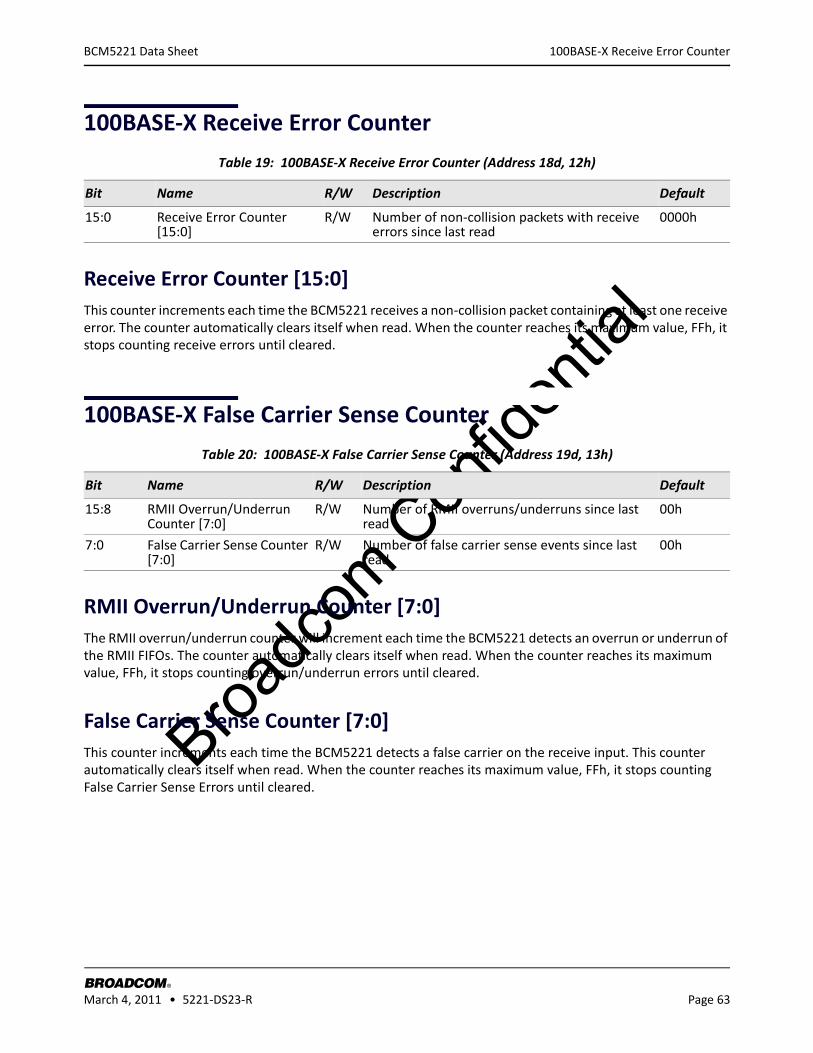
Broadc
om C
onfid
entia
l
100BASE-X Receive Error Counter
BROADCOM March 4, 2011 • 5221-DS23-R Page 63
®
BCM5221 Data Sheet
100BASE-X Receive Error Counter
Receive Error Counter [15:0]This counter increments each time the BCM5221 receives a non-collision packet containing at least one receive error. The counter automatically clears itself when read. When the counter reaches its maximum value, FFh, it stops counting receive errors until cleared.
100BASE-X False Carrier Sense Counter
RMII Overrun/Underrun Counter [7:0]The RMII overrun/underrun counter will increment each time the BCM5221 detects an overrun or underrun of the RMII FIFOs. The counter automatically clears itself when read. When the counter reaches its maximum value, FFh, it stops counting overrun/underrun errors until cleared.
False Carrier Sense Counter [7:0]This counter increments each time the BCM5221 detects a false carrier on the receive input. This counter automatically clears itself when read. When the counter reaches its maximum value, FFh, it stops counting False Carrier Sense Errors until cleared.
Table 19: 100BASE-X Receive Error Counter (Address 18d, 12h)
Bit Name R/W Description Default
15:0 Receive Error Counter [15:0]
R/W Number of non-collision packets with receive errors since last read
0000h
Table 20: 100BASE-X False Carrier Sense Counter (Address 19d, 13h)
Bit Name R/W Description Default
15:8 RMII Overrun/Underrun Counter [7:0]
R/W Number of RMII overruns/underruns since last read
00h
7:0 False Carrier Sense Counter [7:0]
R/W Number of false carrier sense events since last read
00h
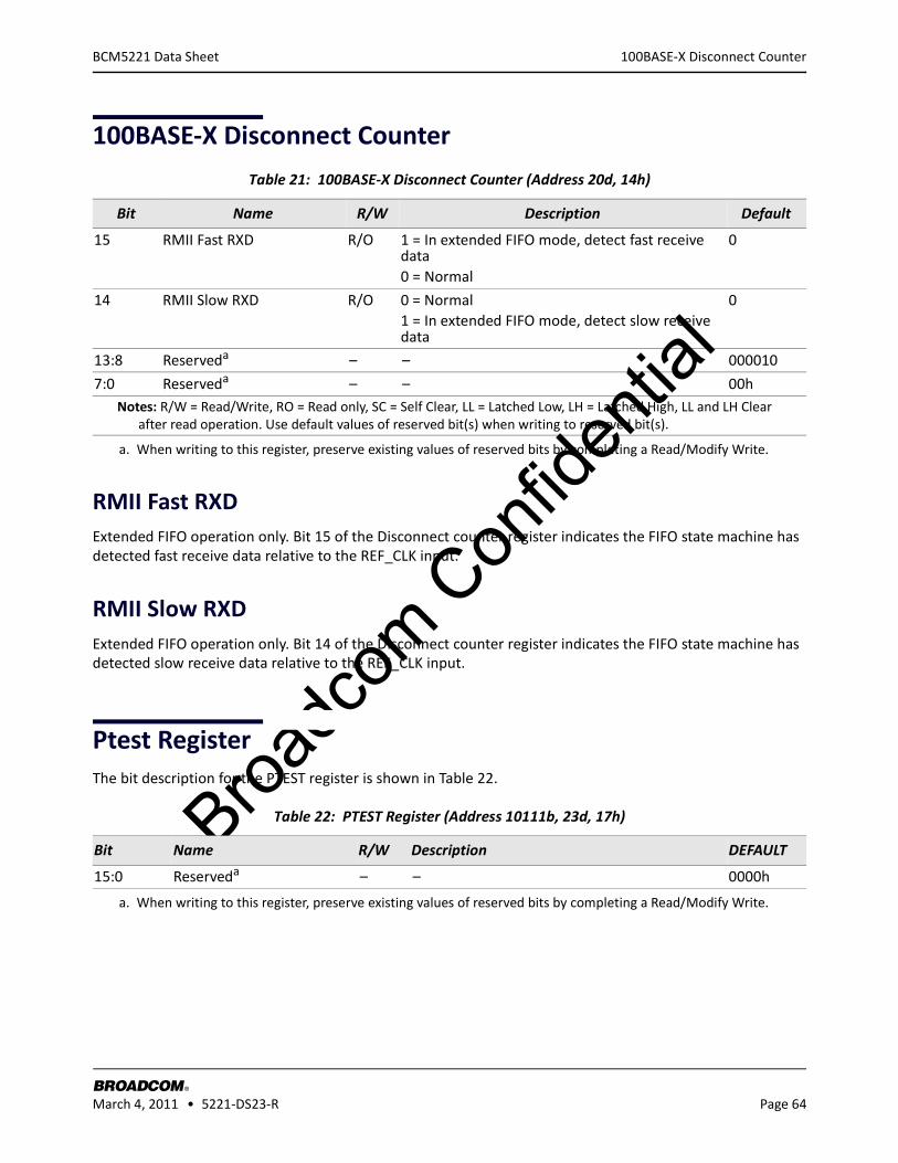
Broadc
om C
onfid
entia
l
100BASE-X Disconnect Counter
BROADCOM March 4, 2011 • 5221-DS23-R Page 64
®
BCM5221 Data Sheet
100BASE-X Disconnect Counter
RMII Fast RXDExtended FIFO operation only. Bit 15 of the Disconnect counter register indicates the FIFO state machine has detected fast receive data relative to the REF_CLK input.
RMII Slow RXDExtended FIFO operation only. Bit 14 of the Disconnect counter register indicates the FIFO state machine has detected slow receive data relative to the REF_CLK input.
Ptest RegisterThe bit description for the PTEST register is shown in Table 22.
Table 21: 100BASE-X Disconnect Counter (Address 20d, 14h)
Bit Name R/W Description Default
15 RMII Fast RXD R/O 1 = In extended FIFO mode, detect fast receive data0 = Normal
0
14 RMII Slow RXD R/O 0 = Normal1 = In extended FIFO mode, detect slow receive data
0
13:8 Reserveda
a. When writing to this register, preserve existing values of reserved bits by completing a Read/Modify Write.
– – 000010
7:0 Reserveda – – 00hNotes: R/W = Read/Write, RO = Read only, SC = Self Clear, LL = Latched Low, LH = Latched High, LL and LH Clear
after read operation. Use default values of reserved bit(s) when writing to reserved bit(s).
Table 22: PTEST Register (Address 10111b, 23d, 17h)
Bit Name R/W Description DEFAULT
15:0 Reserveda
a. When writing to this register, preserve existing values of reserved bits by completing a Read/Modify Write.
– – 0000h
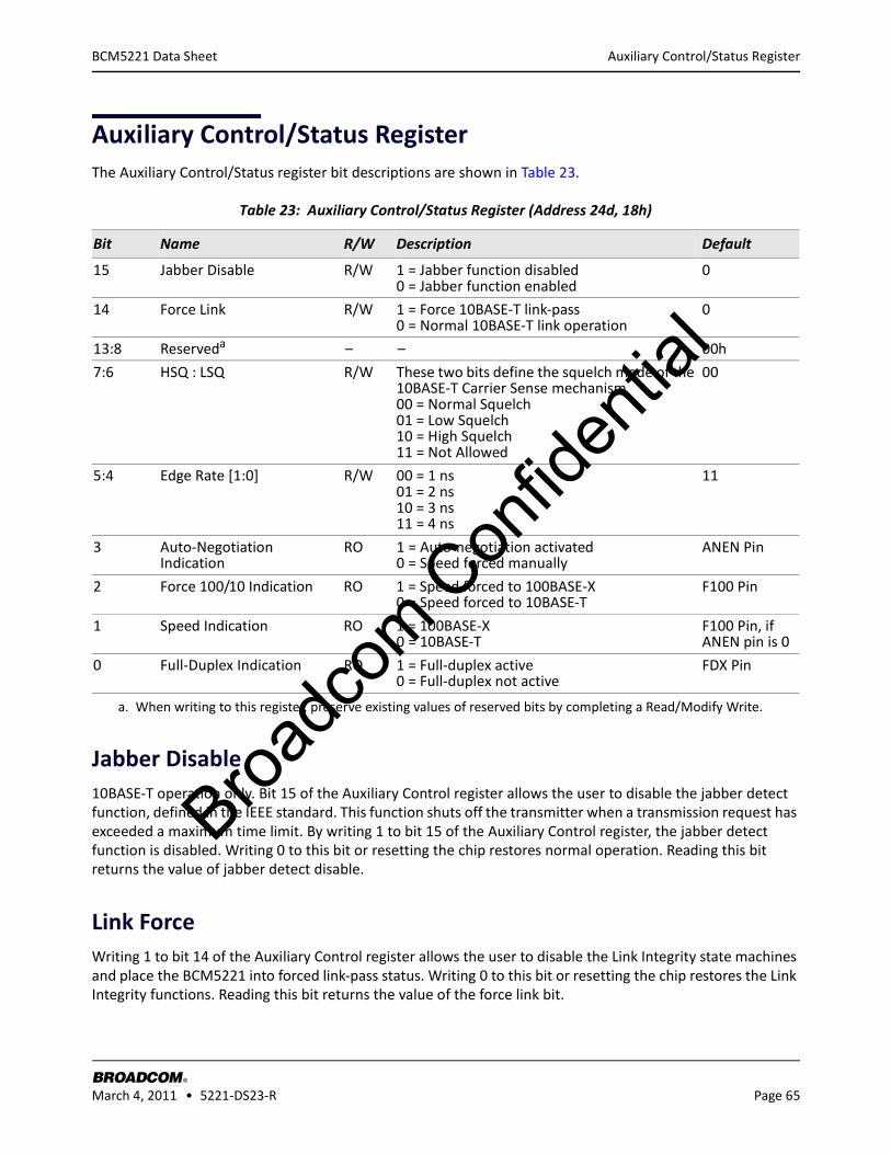
Broadc
om C
onfid
entia
l
Auxiliary Control/Status Register
BROADCOM March 4, 2011 • 5221-DS23-R Page 65
®
BCM5221 Data Sheet
Auxiliary Control/Status RegisterThe Auxiliary Control/Status register bit descriptions are shown in Table 23.
Jabber Disable10BASE-T operation only. Bit 15 of the Auxiliary Control register allows the user to disable the jabber detect function, defined in the IEEE standard. This function shuts off the transmitter when a transmission request has exceeded a maximum time limit. By writing 1 to bit 15 of the Auxiliary Control register, the jabber detect function is disabled. Writing 0 to this bit or resetting the chip restores normal operation. Reading this bit returns the value of jabber detect disable.
Link ForceWriting 1 to bit 14 of the Auxiliary Control register allows the user to disable the Link Integrity state machines and place the BCM5221 into forced link-pass status. Writing 0 to this bit or resetting the chip restores the Link Integrity functions. Reading this bit returns the value of the force link bit.
Table 23: Auxiliary Control/Status Register (Address 24d, 18h)
Bit Name R/W Description Default
15 Jabber Disable R/W 1 = Jabber function disabled 0 = Jabber function enabled
0
14 Force Link R/W 1 = Force 10BASE-T link-pass 0 = Normal 10BASE-T link operation
0
13:8 Reserveda
a. When writing to this register, preserve existing values of reserved bits by completing a Read/Modify Write.
– – 00h
7:6 HSQ : LSQ R/W These two bits define the squelch mode of the 10BASE-T Carrier Sense mechanism 00 = Normal Squelch 01 = Low Squelch 10 = High Squelch 11 = Not Allowed
00
5:4 Edge Rate [1:0] R/W 00 = 1 ns 01 = 2 ns 10 = 3 ns 11 = 4 ns
11
3 Auto-Negotiation Indication
RO 1 = Auto-negotiation activated 0 = Speed forced manually
ANEN Pin
2 Force 100/10 Indication RO 1 = Speed forced to 100BASE-X 0 = Speed forced to 10BASE-T
F100 Pin
1 Speed Indication RO 1 = 100BASE-X 0 = 10BASE-T
F100 Pin, if ANEN pin is 0
0 Full-Duplex Indication RO 1 = Full-duplex active 0 = Full-duplex not active
FDX Pin
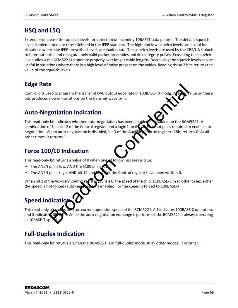
Broadc
om C
onfid
entia
l
Auxiliary Control/Status Register
BROADCOM March 4, 2011 • 5221-DS23-R Page 66
®
BCM5221 Data Sheet
HSQ and LSQExtend or decrease the squelch levels for detection of incoming 10BASET data packets. The default squelch levels implemented are those defined in the IEEE standard. The high-and low-squelch levels are useful for situations where the IEEE-prescribed levels are inadequate. The squelch levels are used by the CRS/LINK block to filter out noise and recognize only valid packet preambles and link integrity pulses. Extending the squelch levels allows the BCM5221 to operate properly over longer cable lengths. Decreasing the squelch levels can be useful in situations where there is a high level of noise present on the cables. Reading these 2 bits returns the value of the squelch levels.
Edge RateControl bits used to program the transmit DAC output edge rate in 100BASE-TX mode. A larger value on these bits produces slower transitions on the transmit waveform.
Auto-Negotiation IndicationThis read-only bit indicates whether auto-negotiation has been enabled or disabled on the BCM5221. A combination of 1 in bit 12 of the Control register and a logic 1 on the ANEN input pin is required to enable auto-negotiation. When auto-negotiation is disabled, bit 3 of the Auxiliary Control register (18h) returns 0. At all other times, it returns 1.
Force 100/10 IndicationThis read-only bit returns a value of 0 when one of following cases is true:
• The ANEN pin is low, AND the F100 pin is low.
• The ANEN pin is high, AND bit 12 and bit 13 of the Control register have been written 0.
When bit 2 of the Auxiliary Control register (18h) is 0, the speed of the chip is 10BASE-T. In all other cases, either the speed is not forced (auto-negotiation is enabled), or the speed is forced to 100BASE-X.
Speed IndicationThis read-only bit shows the true current operation speed of the BCM5221. A 1 indicates 100BASE-X operation, and 0 indicates 10BASE-T. While the auto-negotiation exchange is performed, the BCM5221 is always operating at 10BASE-T speed.
Full-Duplex IndicationThis read-only bit returns 1 when the BCM5221 is in full-duplex mode. In all other modes, it returns 0.
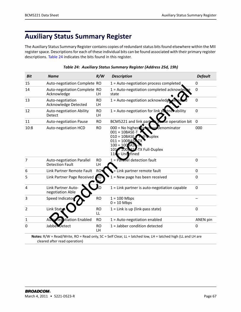
Broadc
om C
onfid
entia
l
Auxiliary Status Summary Register
BROADCOM March 4, 2011 • 5221-DS23-R Page 67
®
BCM5221 Data Sheet
Auxiliary Status Summary RegisterThe Auxiliary Status Summary Register contains copies of redundant status bits found elsewhere within the MII register space. Descriptions for each of these individual bits can be found associated with their primary register descriptions. Table 24 indicates the bits found in this register.
Table 24: Auxiliary Status Summary Register (Address 25d, 19h)
Bit Name R/W Description Default
15 Auto-negotiation Complete RO 1 = Auto-negotiation process completed 0
14 Auto-negotiation Complete Acknowledge
RO LH
1 = Auto-negotiation completed acknowledge state
0
13 Auto-negotiation Acknowledge Detected
RO LH
1 = Auto-negotiation acknowledge detected 0
12 Auto-negotiation Ability Detect
RO LH
1 = Auto-negotiation for link partner ability 0
11 Auto-negotiation Pause RO BCM5221 and link partner pause operation bit 0
10:8 Auto-negotiation HCD RO 000 = No highest common denominator 001 = 10BASE-T 010 = 10BASE-T Full-Duplex 011 = 100BASE-TX 100 = 100BASE-T4 101 = 100BASE-TX Full-Duplex 11x = Undefined
000
7 Auto-negotiation Parallel Detection Fault
RO LH
1 = Parallel detection fault 0
6 Link Partner Remote Fault RO 1 = Link partner remote fault 0
5 Link Partner Page Received RO LH
1 = New page has been received 0
4 Link Partner Auto-negotiation Able
RO 1 = Link partner is auto-negotiation capable 0
3 Speed Indicator RO 1 = 100 Mbps 0 = 10 Mbps
–
2 Link Status RO LL
1 = Link is up (link-pass state) 0
1 Auto-negotiation Enabled RO 1 = Auto-negotiation enabled ANEN pin
0 Jabber Detect RO LH
1 = Jabber condition detected 0
Notes: R/W = Read/Write, RO = Read only, SC = Self Clear, LL = latched low, LH = latched high (LL and LH are cleared after read operation)
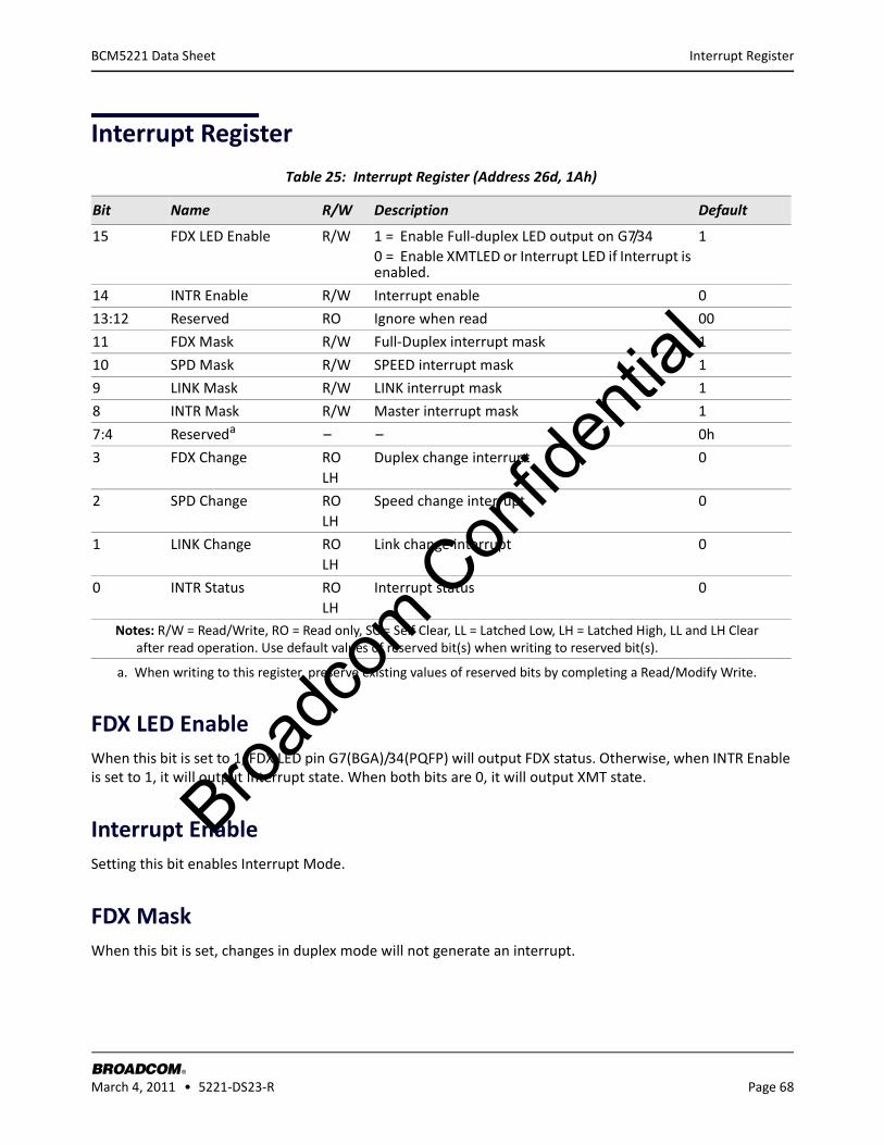
Broadc
om C
onfid
entia
l
Interrupt Register
BROADCOM March 4, 2011 • 5221-DS23-R Page 68
®
BCM5221 Data Sheet
Interrupt Register
FDX LED EnableWhen this bit is set to 1, FDX LED pin G7(BGA)/34(PQFP) will output FDX status. Otherwise, when INTR Enable is set to 1, it will output Interrupt state. When both bits are 0, it will output XMT state.
Interrupt EnableSetting this bit enables Interrupt Mode.
FDX MaskWhen this bit is set, changes in duplex mode will not generate an interrupt.
Table 25: Interrupt Register (Address 26d, 1Ah)
Bit Name R/W Description Default
15 FDX LED Enable R/W 1 = Enable Full-duplex LED output on G7/34 0 = Enable XMTLED or Interrupt LED if Interrupt is enabled.
1
14 INTR Enable R/W Interrupt enable 0
13:12 Reserved RO Ignore when read 00
11 FDX Mask R/W Full-Duplex interrupt mask 1
10 SPD Mask R/W SPEED interrupt mask 1
9 LINK Mask R/W LINK interrupt mask 1
8 INTR Mask R/W Master interrupt mask 1
7:4 Reserveda
a. When writing to this register, preserve existing values of reserved bits by completing a Read/Modify Write.
– – 0h
3 FDX Change ROLH
Duplex change interrupt 0
2 SPD Change ROLH
Speed change interrupt 0
1 LINK Change ROLH
Link change interrupt 0
0 INTR Status ROLH
Interrupt status 0
Notes: R/W = Read/Write, RO = Read only, SC = Self Clear, LL = Latched Low, LH = Latched High, LL and LH Clear after read operation. Use default values of reserved bit(s) when writing to reserved bit(s).

Broadc
om C
onfid
entia
l
Interrupt Register
BROADCOM March 4, 2011 • 5221-DS23-R Page 69
®
BCM5221 Data Sheet
SPD MaskWhen this bit is set, changes in operating speed will not generate an interrupt.
Link MaskWhen this bit is set, changes in Link status will not generate an interrupt.
Interrupt MaskMaster Interrupt Mask. When this bit is set, no interrupts will be generated, regardless of the state of the other MASK bits.
FDX Change1 indicates a change of Duplex status since last register read. Register read clears the bit.
SPD Change1 indicates a change of Speed status since last register read. Register read clears the bit.
Link Change1 indicates a change of Link status since last register read. Register read clears the bit.
Interrupt StatusRepresents status of the INTR# pin. 1 indicates that the interrupt mask is off, and one or more of the change bits are set. Register read clears the bit.
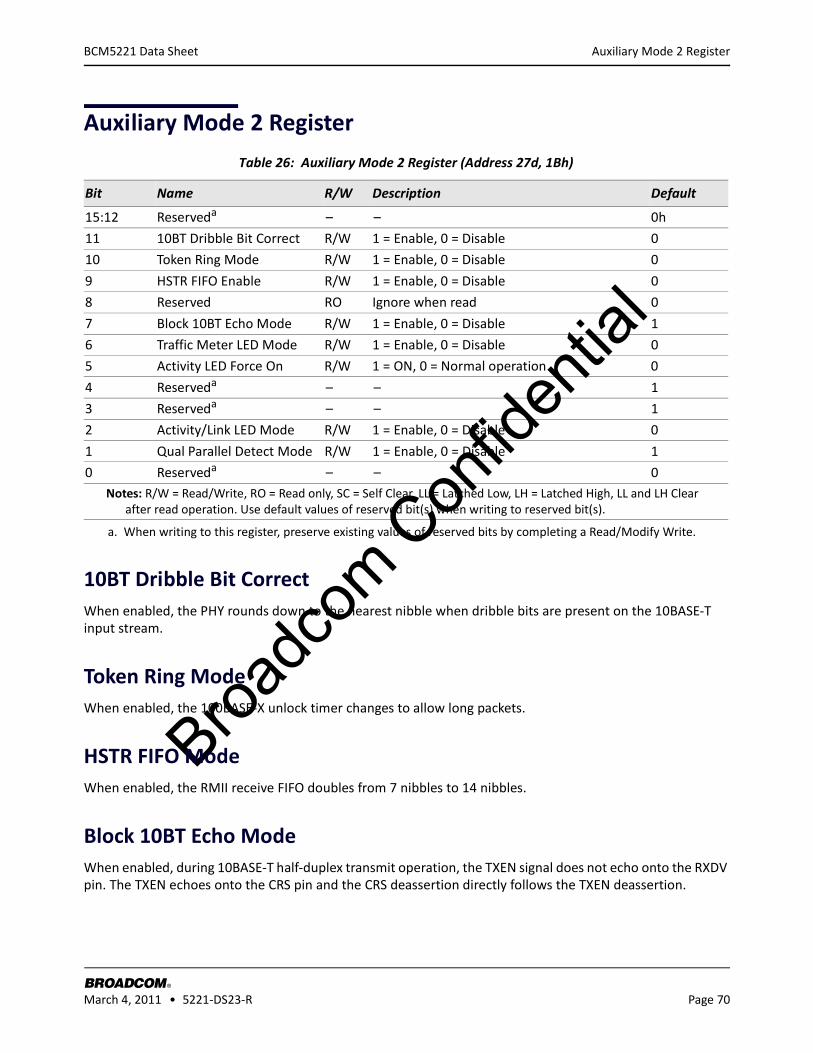
Broadc
om C
onfid
entia
l
Auxiliary Mode 2 Register
BROADCOM March 4, 2011 • 5221-DS23-R Page 70
®
BCM5221 Data Sheet
Auxiliary Mode 2 Register
10BT Dribble Bit CorrectWhen enabled, the PHY rounds down to the nearest nibble when dribble bits are present on the 10BASE-T input stream.
Token Ring ModeWhen enabled, the 100BASE-X unlock timer changes to allow long packets.
HSTR FIFO ModeWhen enabled, the RMII receive FIFO doubles from 7 nibbles to 14 nibbles.
Block 10BT Echo ModeWhen enabled, during 10BASE-T half-duplex transmit operation, the TXEN signal does not echo onto the RXDV pin. The TXEN echoes onto the CRS pin and the CRS deassertion directly follows the TXEN deassertion.
Table 26: Auxiliary Mode 2 Register (Address 27d, 1Bh)
Bit Name R/W Description Default
15:12 Reserveda
a. When writing to this register, preserve existing values of reserved bits by completing a Read/Modify Write.
– – 0h
11 10BT Dribble Bit Correct R/W 1 = Enable, 0 = Disable 0
10 Token Ring Mode R/W 1 = Enable, 0 = Disable 0
9 HSTR FIFO Enable R/W 1 = Enable, 0 = Disable 0
8 Reserved RO Ignore when read 0
7 Block 10BT Echo Mode R/W 1 = Enable, 0 = Disable 1
6 Traffic Meter LED Mode R/W 1 = Enable, 0 = Disable 0
5 Activity LED Force On R/W 1 = ON, 0 = Normal operation 0
4 Reserveda – – 1
3 Reserveda – – 1
2 Activity/Link LED Mode R/W 1 = Enable, 0 = Disable 0
1 Qual Parallel Detect Mode R/W 1 = Enable, 0 = Disable 1
0 Reserveda – – 0Notes: R/W = Read/Write, RO = Read only, SC = Self Clear, LL = Latched Low, LH = Latched High, LL and LH Clear
after read operation. Use default values of reserved bit(s) when writing to reserved bit(s).
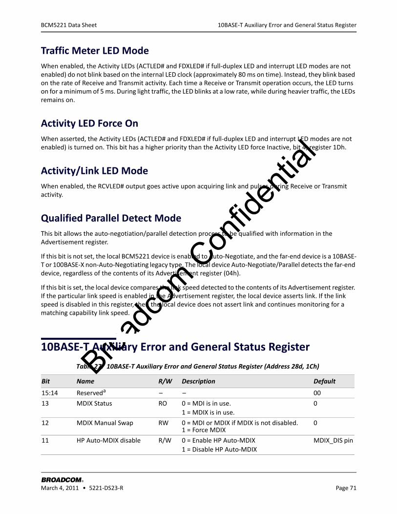
Broadc
om C
onfid
entia
l
10BASE-T Auxiliary Error and General Status Register
BROADCOM March 4, 2011 • 5221-DS23-R Page 71
®
BCM5221 Data Sheet
Traffic Meter LED ModeWhen enabled, the Activity LEDs (ACTLED# and FDXLED# if full-duplex LED and interrupt LED modes are not enabled) do not blink based on the internal LED clock (approximately 80 ms on time). Instead, they blink based on the rate of Receive and Transmit activity. Each time a Receive or Transmit operation occurs, the LED turns on for a minimum of 5 ms. During light traffic, the LED blinks at a low rate, while during heavier traffic, the LEDs remains on.
Activity LED Force OnWhen asserted, the Activity LEDs (ACTLED# and FDXLED# if full-duplex LED and interrupt LED modes are not enabled) is turned on. This bit has a higher priority than the Activity LED force Inactive, bit 4, register 1Dh.
Activity/Link LED ModeWhen enabled, the RCVLED# output goes active upon acquiring link and pulses during Receive or Transmit activity.
Qualified Parallel Detect ModeThis bit allows the auto-negotiation/parallel detection process to be qualified with information in the Advertisement register.
If this bit is not set, the local BCM5221 device is enabled to Auto-Negotiate, and the far-end device is a 10BASE-T or 100BASE-X non-Auto-Negotiating legacy type. The local device Auto-Negotiate/Parallel detects the far-end device, regardless of the contents of its Advertisement register (04h).
If this bit is set, the local device compares the link speed detected to the contents of its Advertisement register. If the particular link speed is enabled in the Advertisement register, the local device asserts link. If the link speed is disabled in this register, then the local device does not assert link and continues monitoring for a matching capability link speed.
10BASE-T Auxiliary Error and General Status Register
Table 27: 10BASE-T Auxiliary Error and General Status Register (Address 28d, 1Ch)
Bit Name R/W Description Default
15:14 Reserveda – – 00
13 MDIX Status RO 0 = MDI is in use.1 = MDIX is in use.
0
12 MDIX Manual Swap RW 0 = MDI or MDIX if MDIX is not disabled. 1 = Force MDIX
0
11 HP Auto-MDIX disable R/W 0 = Enable HP Auto-MDIX1 = Disable HP Auto-MDIX
MDIX_DIS pin
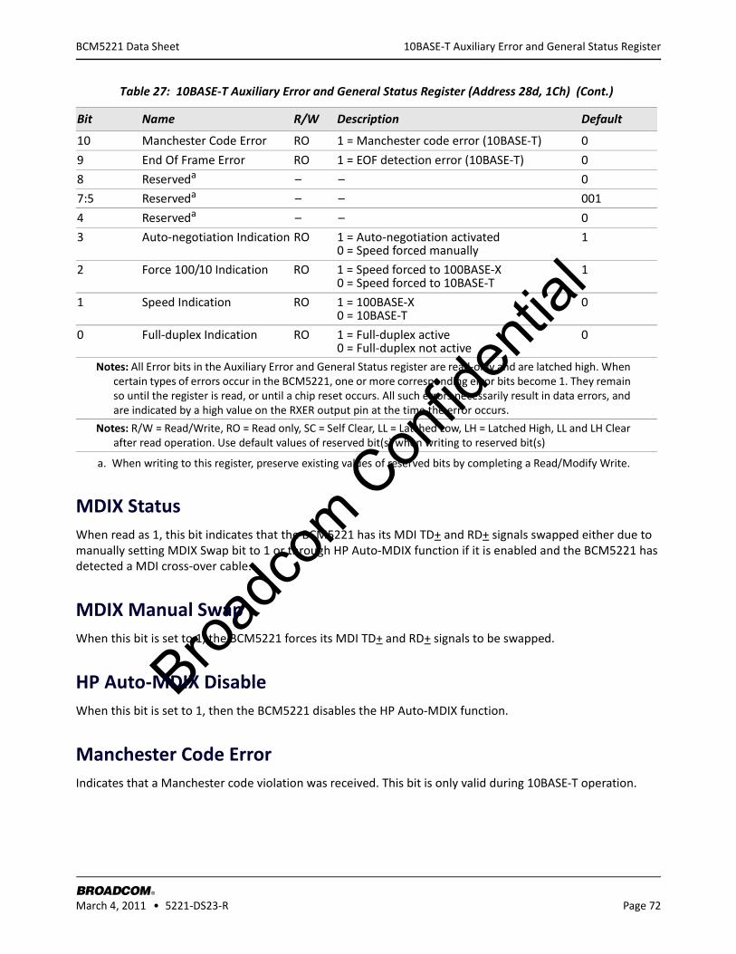
Broadc
om C
onfid
entia
l
10BASE-T Auxiliary Error and General Status Register
BROADCOM March 4, 2011 • 5221-DS23-R Page 72
®
BCM5221 Data Sheet
MDIX StatusWhen read as 1, this bit indicates that the BCM5221 has its MDI TD+ and RD+ signals swapped either due to manually setting MDIX Swap bit to 1 or through HP Auto-MDIX function if it is enabled and the BCM5221 has detected a MDI cross-over cable.
MDIX Manual SwapWhen this bit is set to 1, the BCM5221 forces its MDI TD+ and RD+ signals to be swapped.
HP Auto-MDIX DisableWhen this bit is set to 1, then the BCM5221 disables the HP Auto-MDIX function.
Manchester Code ErrorIndicates that a Manchester code violation was received. This bit is only valid during 10BASE-T operation.
10 Manchester Code Error RO 1 = Manchester code error (10BASE-T) 0
9 End Of Frame Error RO 1 = EOF detection error (10BASE-T) 0
8 Reserveda – – 0
7:5 Reserveda – – 001
4 Reserveda – – 0
3 Auto-negotiation Indication RO 1 = Auto-negotiation activated 0 = Speed forced manually
1
2 Force 100/10 Indication RO 1 = Speed forced to 100BASE-X 0 = Speed forced to 10BASE-T
1
1 Speed Indication RO 1 = 100BASE-X 0 = 10BASE-T
0
0 Full-duplex Indication RO 1 = Full-duplex active 0 = Full-duplex not active
0
Notes: All Error bits in the Auxiliary Error and General Status register are read-only and are latched high. When certain types of errors occur in the BCM5221, one or more corresponding error bits become 1. They remain so until the register is read, or until a chip reset occurs. All such errors necessarily result in data errors, and are indicated by a high value on the RXER output pin at the time the error occurs.
Notes: R/W = Read/Write, RO = Read only, SC = Self Clear, LL = Latched Low, LH = Latched High, LL and LH Clear after read operation. Use default values of reserved bit(s) when writing to reserved bit(s)
a. When writing to this register, preserve existing values of reserved bits by completing a Read/Modify Write.
Table 27: 10BASE-T Auxiliary Error and General Status Register (Address 28d, 1Ch) (Cont.)
Bit Name R/W Description Default
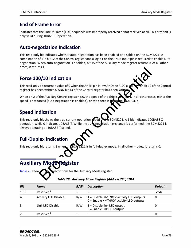
Broadc
om C
onfid
entia
l
Auxiliary Mode Register
BROADCOM March 4, 2011 • 5221-DS23-R Page 73
®
BCM5221 Data Sheet
End of Frame ErrorIndicates that the End Of Frame (EOF) sequence was improperly received or not received at all. This error bit is only valid during 10BASE-T operation.
Auto-negotiation IndicationThis read-only bit indicates whether auto-negotiation has been enabled or disabled on the BCM5221. A combination of 1 in bit 12 of the Control register and a logic 1 on the ANEN input pin is required to enable auto-negotiation. When auto-negotiation is disabled, bit 15 of the Auxiliary Mode register returns 0. At all other times, it returns 1.
Force 100/10 IndicationThis read-only bit returns a value of 0 when the ANEN pin is low AND the F100 pin is low, or Bit 12 of the Control register has been written 0 AND bit 13 of the Control register has been written 0.
When bit 2 of the Auxiliary Control register is 0, the speed of the chip is 10BASE-T. In all other cases, either the speed is not forced (auto-negotiation is enabled), or the speed is forced to 100BASE-X.
Speed IndicationThis read-only bit shows the true current operation speed of the BCM5221. A 1 bit indicates 100BASE-X operation, while 0 indicates 10BASE-T. While the auto-negotiation exchange is performed, the BCM5221 is always operating at 10BASE-T speed.
Full-Duplex IndicationThis read-only bit returns 1 when the BCM5221 is in full-duplex mode. In all other modes, it returns 0.
Auxiliary Mode RegisterTable 28 shows the bit descriptions for the Auxiliary Mode register.
Table 28: Auxiliary Mode Register (Address 29d, 1Dh)
Bit Name R/W Description Default
15:5 Reserveda – – xxxh
4 Activity LED Disable R/W 1 = Disable XMT/RCV activity LED outputs 0 = Enable XMT/RCV activity LED outputs
0
3 Link LED Disable R/W 1 = Disable link LED output 0 = Enable link LED output
0
2 Reserveda – – 0
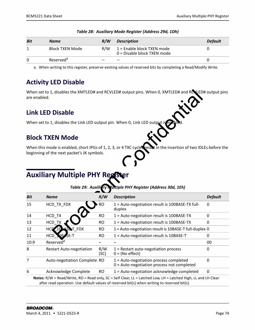
Broadc
om C
onfid
entia
l
Auxiliary Multiple PHY Register
BROADCOM March 4, 2011 • 5221-DS23-R Page 74
®
BCM5221 Data Sheet
Activity LED DisableWhen set to 1, disables the XMTLED# and RCVLED# output pins. When 0, XMTLED# and RCVLED# output pins are enabled.
Link LED DisableWhen set to 1, disables the Link LED output pin. When 0, Link LED output is enabled.
Block TXEN ModeWhen this mode is enabled, short IPGs of 1, 2, 3, or 4 TXC cycles result in the insertion of two IDLEs before the beginning of the next packet’s JK symbols.
Auxiliary Multiple PHY Register
1 Block TXEN Mode R/W 1 = Enable block TXEN mode 0 = Disable block TXEN mode
0
0 Reserveda – – 0
a. When writing to this register, preserve existing values of reserved bits by completing a Read/Modify Write.
Table 29: Auxiliary Multiple PHY Register (Address 30d, 1Eh)
Bit Name R/W Description Default
15 HCD_TX_FDX RO 1 = Auto-negotiation result is 100BASE-TX full-duplex
0
14 HCD_T4 RO 1 = Auto-negotiation result is 100BASE-T4 0
13 HCD_TX RO 1 = Auto-negotiation result is 100BASE-TX 0
12 HCD_10BASE-T_FDX RO 1 = Auto-negotiation result is 10BASE-T full-duplex 0
11 HCD_10BASE-T RO 1 = Auto-negotiation result is 10BASE-T 0
10:9 Reserveda – – 00
8 Restart Auto-negotiation R/W (SC)
1 = Restart auto-negotiation process 0 = (No effect)
0
7 Auto-negotiation Complete RO 1 = Auto-negotiation process completed 0 = Auto-negotiation process not completed
0
6 Acknowledge Complete RO 1 = Auto-negotiation acknowledge completed 0Notes: R/W = Read/Write, RO = Read only, SC = Self Clear, LL = Latched Low, LH = Latched High, LL and LH Clear
after read operation. Use default values of reserved bit(s) when writing to reserved bit(s).
Table 28: Auxiliary Mode Register (Address 29d, 1Dh)
Bit Name R/W Description Default
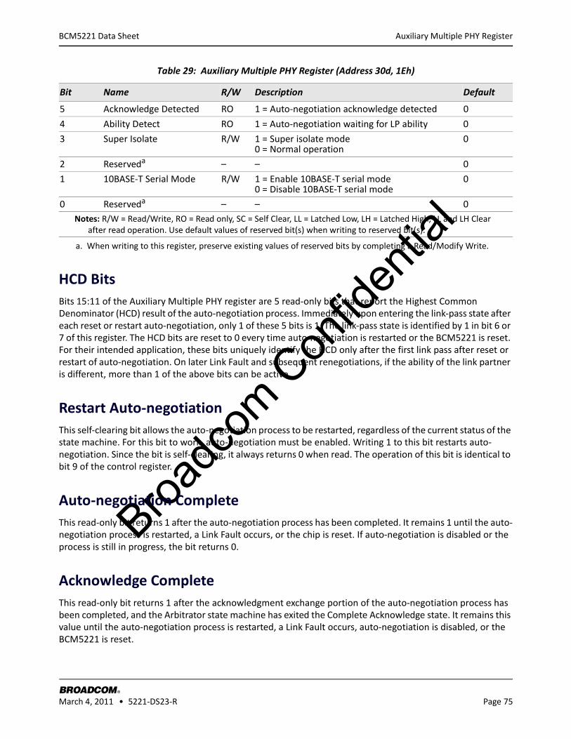
Broadc
om C
onfid
entia
l
Auxiliary Multiple PHY Register
BROADCOM March 4, 2011 • 5221-DS23-R Page 75
®
BCM5221 Data Sheet
HCD BitsBits 15:11 of the Auxiliary Multiple PHY register are 5 read-only bits that report the Highest Common Denominator (HCD) result of the auto-negotiation process. Immediately upon entering the link-pass state after each reset or restart auto-negotiation, only 1 of these 5 bits is 1. The link-pass state is identified by 1 in bit 6 or 7 of this register. The HCD bits are reset to 0 every time auto-negotiation is restarted or the BCM5221 is reset. For their intended application, these bits uniquely identify the HCD only after the first link pass after reset or restart of auto-negotiation. On later Link Fault and subsequent renegotiations, if the ability of the link partner is different, more than 1 of the above bits can be active.
Restart Auto-negotiationThis self-clearing bit allows the auto-negotiation process to be restarted, regardless of the current status of the state machine. For this bit to work, auto-negotiation must be enabled. Writing 1 to this bit restarts auto-negotiation. Since the bit is self-clearing, it always returns 0 when read. The operation of this bit is identical to bit 9 of the control register.
Auto-negotiation CompleteThis read-only bit returns 1 after the auto-negotiation process has been completed. It remains 1 until the auto-negotiation process is restarted, a Link Fault occurs, or the chip is reset. If auto-negotiation is disabled or the process is still in progress, the bit returns 0.
Acknowledge CompleteThis read-only bit returns 1 after the acknowledgment exchange portion of the auto-negotiation process has been completed, and the Arbitrator state machine has exited the Complete Acknowledge state. It remains this value until the auto-negotiation process is restarted, a Link Fault occurs, auto-negotiation is disabled, or the BCM5221 is reset.
5 Acknowledge Detected RO 1 = Auto-negotiation acknowledge detected 0
4 Ability Detect RO 1 = Auto-negotiation waiting for LP ability 0
3 Super Isolate R/W 1 = Super isolate mode 0 = Normal operation
0
2 Reserveda – – 0
1 10BASE-T Serial Mode R/W 1 = Enable 10BASE-T serial mode 0 = Disable 10BASE-T serial mode
0
0 Reserveda – – 0
a. When writing to this register, preserve existing values of reserved bits by completing a Read/Modify Write.
Table 29: Auxiliary Multiple PHY Register (Address 30d, 1Eh)
Bit Name R/W Description Default
Notes: R/W = Read/Write, RO = Read only, SC = Self Clear, LL = Latched Low, LH = Latched High, LL and LH Clear after read operation. Use default values of reserved bit(s) when writing to reserved bit(s).
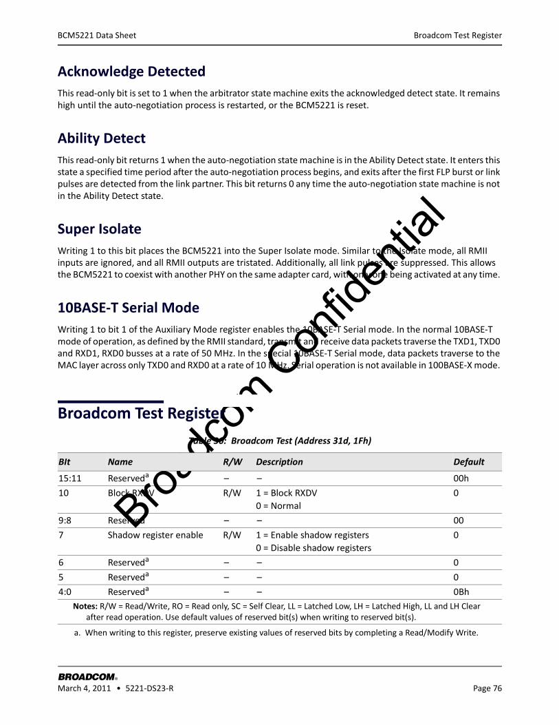
Broadc
om C
onfid
entia
l
Broadcom Test Register
BROADCOM March 4, 2011 • 5221-DS23-R Page 76
®
BCM5221 Data Sheet
Acknowledge DetectedThis read-only bit is set to 1 when the arbitrator state machine exits the acknowledged detect state. It remains high until the auto-negotiation process is restarted, or the BCM5221 is reset.
Ability DetectThis read-only bit returns 1 when the auto-negotiation state machine is in the Ability Detect state. It enters this state a specified time period after the auto-negotiation process begins, and exits after the first FLP burst or link pulses are detected from the link partner. This bit returns 0 any time the auto-negotiation state machine is not in the Ability Detect state.
Super IsolateWriting 1 to this bit places the BCM5221 into the Super Isolate mode. Similar to the Isolate mode, all RMII inputs are ignored, and all RMII outputs are tristated. Additionally, all link pulses are suppressed. This allows the BCM5221 to coexist with another PHY on the same adapter card, with only one being activated at any time.
10BASE-T Serial ModeWriting 1 to bit 1 of the Auxiliary Mode register enables the 10BASE-T Serial mode. In the normal 10BASE-T mode of operation, as defined by the RMII standard, transmit and receive data packets traverse the TXD1, TXD0 and RXD1, RXD0 busses at a rate of 50 MHz. In the special 10BASE-T Serial mode, data packets traverse to the MAC layer across only TXD0 and RXD0 at a rate of 10 MHz. Serial operation is not available in 100BASE-X mode.
Broadcom Test Register
Table 30: Broadcom Test (Address 31d, 1Fh)
BIt Name R/W Description Default
15:11 Reserveda
a. When writing to this register, preserve existing values of reserved bits by completing a Read/Modify Write.
– – 00h
10 Block RXDV R/W 1 = Block RXDV0 = Normal
0
9:8 Reserved – – 00
7 Shadow register enable R/W 1 = Enable shadow registers0 = Disable shadow registers
0
6 Reserveda – – 0
5 Reserveda – – 0
4:0 Reserveda – – 0BhNotes: R/W = Read/Write, RO = Read only, SC = Self Clear, LL = Latched Low, LH = Latched High, LL and LH Clear
after read operation. Use default values of reserved bit(s) when writing to reserved bit(s).
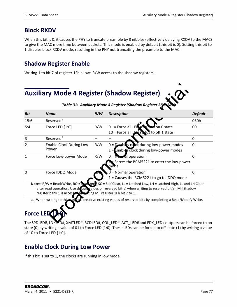
Broadc
om C
onfid
entia
l
Auxiliary Mode 4 Register (Shadow Register)
BROADCOM March 4, 2011 • 5221-DS23-R Page 77
®
BCM5221 Data Sheet
Block RXDVWhen this bit is 0, it causes the PHY to truncate preamble by 8 nibbles (effectively delaying RXDV to the MAC) to give the MAC more time between packets. This mode is enabled by default (this bit is 0). Setting this bit to 1 disables block RXDV mode, resulting in the PHY not truncating the preamble to the MAC.
Shadow Register EnableWriting 1 to bit 7 of register 1Fh allows R/W access to the shadow registers.
Auxiliary Mode 4 Register (Shadow Register)
Force LED [1:0]The SPDLED#, LNKLED#, XMTLED#, RCDLED#, COL_LED#, ACT_LED# and FDX_LED# outputs can be forced to on state (0) by writing a value of 01 to Force LED [1:0]. These LEDs can be forced to off state (1) by writing a value of 10 to Force LED {1:0].
Enable Clock During Low PowerIf this bit is set to 1, the clocks are running in low mode.
Table 31: Auxiliary Mode 4 Register (Shadow Register 26d, 1Ah)
BIt Name R/W Description Default
15:6 Reserveda
a. When writing to this register, preserve existing values of reserved bits by completing a Read/Modify Write.
– – 030h
5:4 Force LED [1:0] R/W 01 = Force all LED status to on 0 state10 = Force all LED status to off 1 state
00
3 Reserveda – – 0
2 Enable Clock During Low Power
R/W 0 = Disables clock during low-power modes1 = Enables clock during low-power modes
0
1 Force Low-power Mode R/W 0 = Normal operation1 = Forces the BCM5221 to enter the low-power mode
0
0 Force IDDQ Mode R/W 0 = Normal operation1 = Causes the BCM5221 to go to IDDQ mode
0
Notes: R/W = Read/Write, RO = Read only, SC = Self Clear, LL = Latched Low, LH = Latched High, LL and LH Clear after read operation. Use default values of reserved bit(s) when writing to reserved bit(s). MII Shadow register bank 1 is accessed by setting MII register 1Fh bit 7 to 1.
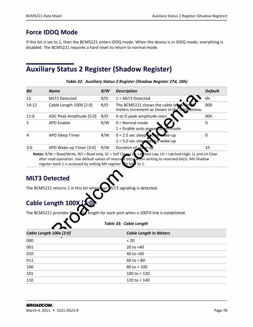
Broadc
om C
onfid
entia
l
Auxiliary Status 2 Register (Shadow Register)
BROADCOM March 4, 2011 • 5221-DS23-R Page 78
®
BCM5221 Data Sheet
Force IDDQ ModeIf this bit is set to 1, then the BCM5221 enters IDDQ mode. When the device is in IDDQ mode, everything is disabled. The BCM5221 requires a hard reset to return to normal mode.
Auxiliary Status 2 Register (Shadow Register)
MLT3 DetectedThe BCM5221 returns 1 in this bit whenever MLT3 signaling is detected.
Cable Length 100X [2:0]The BCM5221 provides the cable length for each port when a 100TX link is established.
Table 32: Auxiliary Status 2 Register (Shadow Register 27d, 1Bh)
Bit Name R/W Description Default
15 MLT3 Detected R/O 1 = MLT3 Detected 0h
14:12 Cable Length 100X [2:0] R/O The BCM5221 shows the cable length in 20 meters increment as shown in the table below.
000
11:6 ADC Peak Amplitude [5:0] R/O A to D peak amplitude seen 00h
5 APD Enable R/W 0 = Normal mode1 = Enable auto power-down mode
0
4 APD Sleep Timer R/W 0 = 2.5 sec sleep before wake-up1 = 5.0 sec sleep before wake-up
0
3:0 APD Wake-up Timer [3:0] R/W Duration of wake-up 1hNotes: R/W = Read/Write, RO = Read only, SC = Self Clear, LL = Latched Low, LH = Latched High, LL and LH Clear
after read operation. Use default values of reserved bit(s) when writing to reserved bit(s). MII Shadow register bank 1 is accessed by setting MII register 1Fh bit 7 to 1.
Table 33: Cable Length
Cable Length 100x [2:0] Cable Length In Meters
000 < 20
001 20 to <40
010 40 to <60
011 60 to < 80
100 80 to < 100
101 100 to < 120
110 120 to < 140
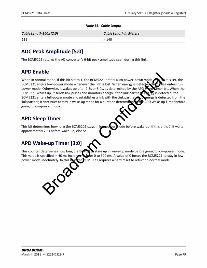
Broadc
om C
onfid
entia
l
Auxiliary Status 2 Register (Shadow Register)
BROADCOM March 4, 2011 • 5221-DS23-R Page 79
®
BCM5221 Data Sheet
ADC Peak Amplitude [5:0]The BCM5221 returns the AD converter’s 6-bit peak amplitude seen during this link.
APD EnableWhen in normal mode, if this bit set to 1, the BCM5221 enters auto power-down mode. If this bit is set, the BCM5221 enters low-power mode whenever the link is lost. When energy is detected the device enters full-power mode. Otherwise, it wakes up after 2.5s or 5.0s, as determined by the APD Sleep Timer bit. When the BCM5221 wakes up, it sends link pulses and monitors energy. If the link partner’s energy is detected, the BCM5221 enters full-power mode and establishes a link with the Link partner. If no energy is detected from the link partner, it continues to stay in wake-up mode for a duration determined by the APD Wake-up Timer before going to low-power mode.
APD Sleep TImerThis bit determines how long the BCM5221 stays in low-power mode before wake-up. If this bit is 0, it waits approximately 2.5s before wake-up, else 5s.
APD Wake-up TImer [3:0]This counter determines how long the BCM5221 stays up in wake-up mode before going to low-power mode. This value is specified in 40 ms increments from 0 to 600 ms. A value of 0 forces the BCM5221 to stay in low-power mode indefinitely. In this case the BCM5221 requires a hard reset to return to normal mode.
111 > 140
Table 33: Cable Length
Cable Length 100x [2:0] Cable Length In Meters
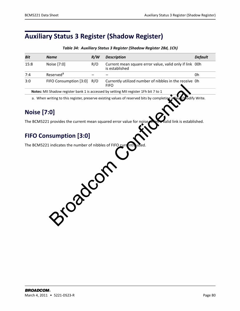
Broadc
om C
onfid
entia
l
Auxiliary Status 3 Register (Shadow Register)
BROADCOM March 4, 2011 • 5221-DS23-R Page 80
®
BCM5221 Data Sheet
Auxiliary Status 3 Register (Shadow Register)
Noise [7:0]The BCM5221 provides the current mean squared error value for noise when a valid link is established.
FIFO Consumption [3:0]The BCM5221 indicates the number of nibbles of FIFO currently used.
Table 34: Auxiliary Status 3 Register (Shadow Register 28d, 1Ch)
Bit Name R/W Description Default
15:8 Noise [7:0] R/O Current mean square error value, valid only if link is established
00h
7:4 Reserveda
a. When writing to this register, preserve existing values of reserved bits by completing a Read/Modify Write.
– – 0h
3:0 FIFO Consumption [3:0] R/O Currently utilized number of nibbles in the receive FIFO
0h
Notes: MII Shadow register bank 1 is accessed by setting MII register 1Fh bit 7 to 1
Broadc
om C
onfid
entia
l
Auxiliary Mode 3 Register (Shadow Register)
BROADCOM March 4, 2011 • 5221-DS23-R Page 81
®
BCM5221 Data Sheet
Auxiliary Mode 3 Register (Shadow Register)
FIFO Size Select [3:0]The BCM5221 indicates the current selection of receive FIFO size using bit 3 through 0 as shown in Table 36. The size can also be determined by bit “Extended RMII FIFO Enable” on page 60.
Table 35: Auxiliary Mode 3 Register (Shadow Register 29d, 1Dh)
Bit Name R/W Description Default
15:4 Reserveda
a. When writing to this register, preserve existing values of reserved bits by completing a Read/Modify Write.
– – 000h
3:0 FIFO Size Select [3:0] R/W Currently selected receive FIFO Size 4hNotes: R/W = Read/Write, RO = Read only, SC = Self Clear, LL = Latched Low, LH = Latched High, LL and LH Clear
after read operation. Use default values of reserved bit(s) when writing to reserved bit(s). MII Shadow register bank 1 is accessed by setting MII register 1Fh bit 7 to 1.
Table 36: Current Receive FIFO Size
FIFO Size Select [3:0]Receive FIFO Size in Use(# of bits)
0001 16
0010 20
0011 24
0100 28
0101 32
0110 36
0111 40
1000 44
1001 48
1010 52
1011 56
1100 60
1101 64

Broadc
om C
onfid
entia
l
Auxiliary Status 4 Register (Shadow Register)
BROADCOM March 4, 2011 • 5221-DS23-R Page 82
®
BCM5221 Data Sheet
Auxiliary Status 4 Register (Shadow Register)
Packet Length Counter [15:0]The BCM5221 shows the number of bytes in the last packet received. This is valid only when a valid link is established.
Table 37: Auxiliary Status 4 Register (Shadow Register 30d, 1Eh)
Bit Name R/W Description Default
15:0 Packet Length Counter[15:0]
R/O Number of bytes in the last received packet 0000h
Broadc
om C
onfid
entia
l
Timing and AC Characteristics
BROADCOM March 4, 2011 • 5221-DS23-R Page 83
®
BCM5221 Data Sheet
Section 6: T iming and AC Characteristics
The timing information contained in this section applies to the BCM5221.
All MII Interface pins comply with IEEE 802.3u timing specifications (see Reconciliation Sublayer and Media Independent Interface in IEEE 802.3u timing specifications). All digital output timing specified at CL = 30 pF.
Output rise/fall times measured between 10% and 90% of the output signal swing. Input rise/fall times measured between VIL max. and VIH min. Output signal transitions referenced to the midpoint of the output signal swing. Input signal transitions referenced to the midpoint between VIL max. and VIH min. See Table 38 and Table 39 for the timing parameters. See Figure 5 for an illustration of clock and reset timing.
Table 38: Clock Timing
Parameter Symbol Min Typ Max Unit
XTALI Cycle Time CK_CYCLE 39.998 40 40.002 ns
XTALI High/Low Time CK_HI CK_LO
14 20 26 ns
REF_CLK Cycle Time (MII - 25 MHz) – – 40 – ns
REF_CLK High/Low Time (MII - 25 MHz) – 13 20 27 ns
REF_CLK Rise/Fall Time (MII - 25 MHz) – – – 4 ns
REF_CLK Cycle Time (RMII - 50 MHz) – – 20 2 ns
REF_CLK High/Low Time (RMII - 50 MHz) – 7 10 13 ns
REF_CLK Rise/Fall Time (RMII - 50 MHz) – – – 2 ns
Table 39: Reset Timinga
a. If the reference clock is not supplied at power-on, the chip can enter low-power mode. To exit low-power mode, it is necessary to input the reset with reference clock for at least 20 μs.
Parameter Symbol Min Typ Max Unit
Reset Pulse Length with stable XTALI Inputb
b. During power-on, RESET# pin must be held low to get the BCM5221 to power-up in normal mode.
RESET_LEN 400 – – ns
Activity after end of Hardware Reset RESET_WAIT 100 – – μs
RESET# Rise/Fall Time RESET_EDGE – – 10 ns
Broadc
om C
onfid
entia
l
Timing and AC Characteristics
BROADCOM March 4, 2011 • 5221-DS23-R Page 84
®
BCM5221 Data Sheet
Figure 5: Clock and Reset Timing
Table 40 provides the parameters for 100BASE-X transmit timing. Figure 6 illustrates the 100BASE-TX transmit start of packet timing and Figure 7 on page 85 shows the100BASE-TX transmit end of packet timing.
Table 40: MII 100BASE-X Transmit Timing
Parameter Symbol Min Typ Max Unit
TXC Cycle Time – – 40 – ns
TXC High/Low Time – 16 20 24 ns
TXC Rise/Fall Time – 2 – 5 ns
TXEN, TXD[3:0] Setup Time to TXC rising TXEN_SETUP 10 – – ns
TXEN, TXD[3:0] Hold Time from TXC rising TXEN_HOLD 0 – – ns
TD± after TXEN Assert (unsampled) TXEN_TDATA – 100 – ns
TXD to TD± Steady State Delay TXD_TDATA – 100 – ns
CRS Assert after TXEN Assert TXEN_CRS – 11 – ns
CRS Deassert after TXEN Deassert TXEN_CRS_EOP – 11 – ns
COL Assert after TXEN Assert (while RX) TXEN_COL – 17 – ns
COL Deassert after TXEN Deassert (while RX) TXEN_COL_EOP – 17 – ns
XTALI
RESET#
Normal PHY
RESET_LEN RESET_WAIT
CK_HI
CK_CYCLE
CK_EDGE
CK_LO
CK_EDGE
activity begins here RESET_EDGE
RESET_EDGE
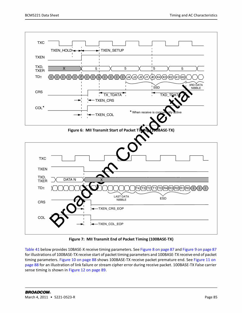
Broadc
om C
onfid
entia
l
Timing and AC Characteristics
BROADCOM March 4, 2011 • 5221-DS23-R Page 85
®
BCM5221 Data Sheet
Figure 6: MII Transmit Start of Packet Timing (100BASE-TX)
Figure 7: MII Transmit End of Packet Timing (100BASE-TX)
Table 41 below provides 10BASE-X receive timing parameters. See Figure 8 on page 87 and Figure 9 on page 87 for illustrations of 100BASE-TX receive start of packet timing parameters and 100BASE-TX receive end of packet timing parameters. Figure 10 on page 88 shows 100BASE-TX receive packet premature end. See Figure 11 on page 88 for an illustration of link failure or stream cipher error during receive packet. 100BASE-TX False carrier sense timing is shown in Figure 12 on page 89.
5 5 5 5
TX_TDATA
TXEN_CRS
TXEN_COL
TXD_TDATA
SSD3RD DATA
NIBBLE
COL** When receive is concurrently active
I I I I J4 J3 J2 K4 K3 K2 K1 K0
CRS
TD±
TXER
TXEN
TXD,
J1
TXEN_SETUP
IIIIIIIII
X
J0
TXEN_HOLD
TXC
ESD
TXEN_CRS_EOP
TXEN_COL_EOP
LAST DATA
DATA N
T4 T3 T2 T1 T0 R4 R3 R2 R1 R0
NIBBLE
TD±
TXD,TXER
COL
TXEN
CRS
IIII
X
TXC
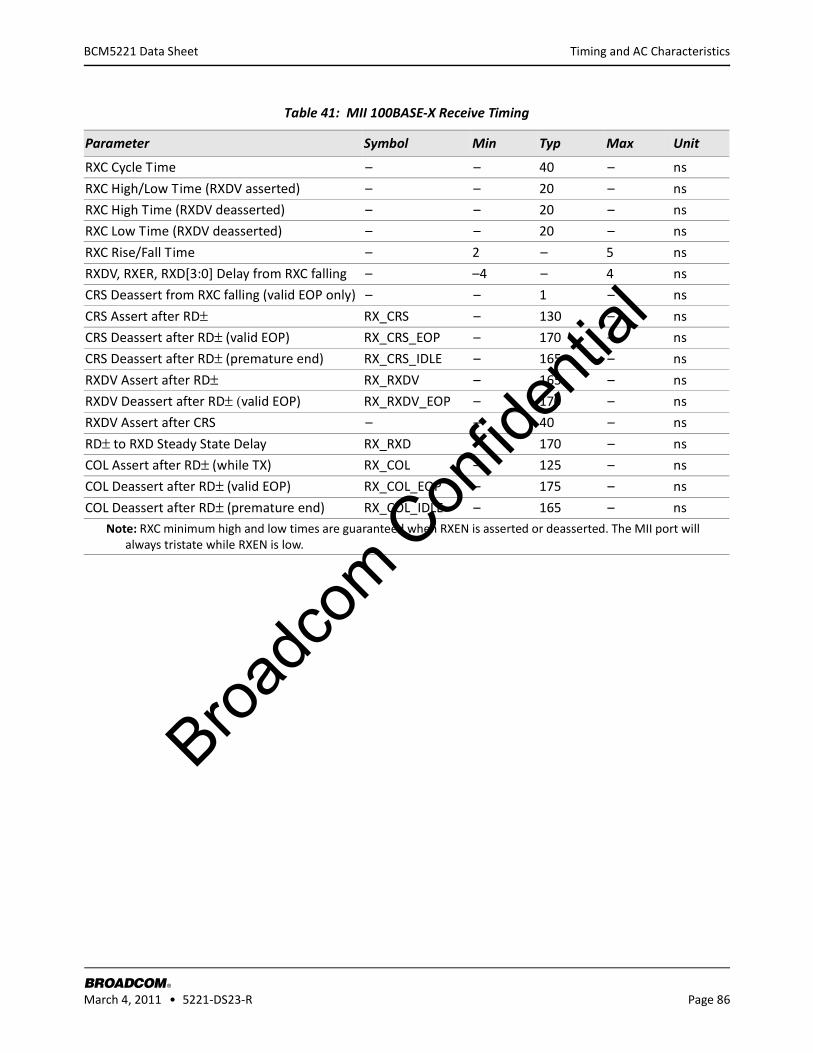
Broadc
om C
onfid
entia
l
Timing and AC Characteristics
BROADCOM March 4, 2011 • 5221-DS23-R Page 86
®
BCM5221 Data Sheet
Table 41: MII 100BASE-X Receive Timing
Parameter Symbol Min Typ Max Unit
RXC Cycle Time – – 40 – ns
RXC High/Low Time (RXDV asserted) – – 20 – ns
RXC High Time (RXDV deasserted) – – 20 – ns
RXC Low Time (RXDV deasserted) – – 20 – ns
RXC Rise/Fall Time – 2 – 5 ns
RXDV, RXER, RXD[3:0] Delay from RXC falling – –4 – 4 ns
CRS Deassert from RXC falling (valid EOP only) – – 1 – ns
CRS Assert after RD± RX_CRS – 130 – ns
CRS Deassert after RD± (valid EOP) RX_CRS_EOP – 170 – ns
CRS Deassert after RD± (premature end) RX_CRS_IDLE – 165 – ns
RXDV Assert after RD± RX_RXDV – 165 – ns
RXDV Deassert after RD± (valid EOP) RX_RXDV_EOP – 170 – ns
RXDV Assert after CRS – – 40 – ns
RD± to RXD Steady State Delay RX_RXD – 170 – ns
COL Assert after RD± (while TX) RX_COL – 125 – ns
COL Deassert after RD± (valid EOP) RX_COL_EOP – 175 – ns
COL Deassert after RD± (premature end) RX_COL_IDLE – 165 – nsNote: RXC minimum high and low times are guaranteed when RXEN is asserted or deasserted. The MII port will
always tristate while RXEN is low.
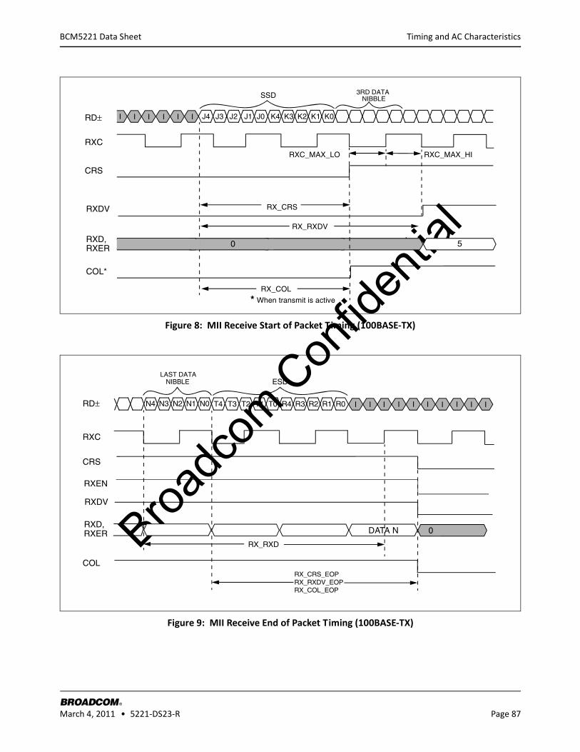
Broadc
om C
onfid
entia
l
Timing and AC Characteristics
BROADCOM March 4, 2011 • 5221-DS23-R Page 87
®
BCM5221 Data Sheet
Figure 8: MII Receive Start of Packet Timing (100BASE-TX)
Figure 9: MII Receive End of Packet Timing (100BASE-TX)
RX_CRS
RX_COL
3RD DATA SSD
RX_RXDV
NIBBLE
* When transmit is active
J4 J3 J2 K4 K3 K2 K1 K0J1 J0I I I IIII
0 5
COL*
RXDV
RXD,
RD±
RXC
CRS
RXER
RXC_MAX_HIRXC_MAX_LO
LAST DATA
COL
RXDV
RXD,
RD±
RXC
CRS
ESD
RX_CRS_EOP
RX_COL_EOP
N4 N3 N2 N1 N0 T4 T3 T2 T1 T0 R4 R3 R2 R1 R0
RXER
NIBBLE
DATA N
RX_RXD
IIIIIIIIII
RX_RXDV_EOP
0
RXEN
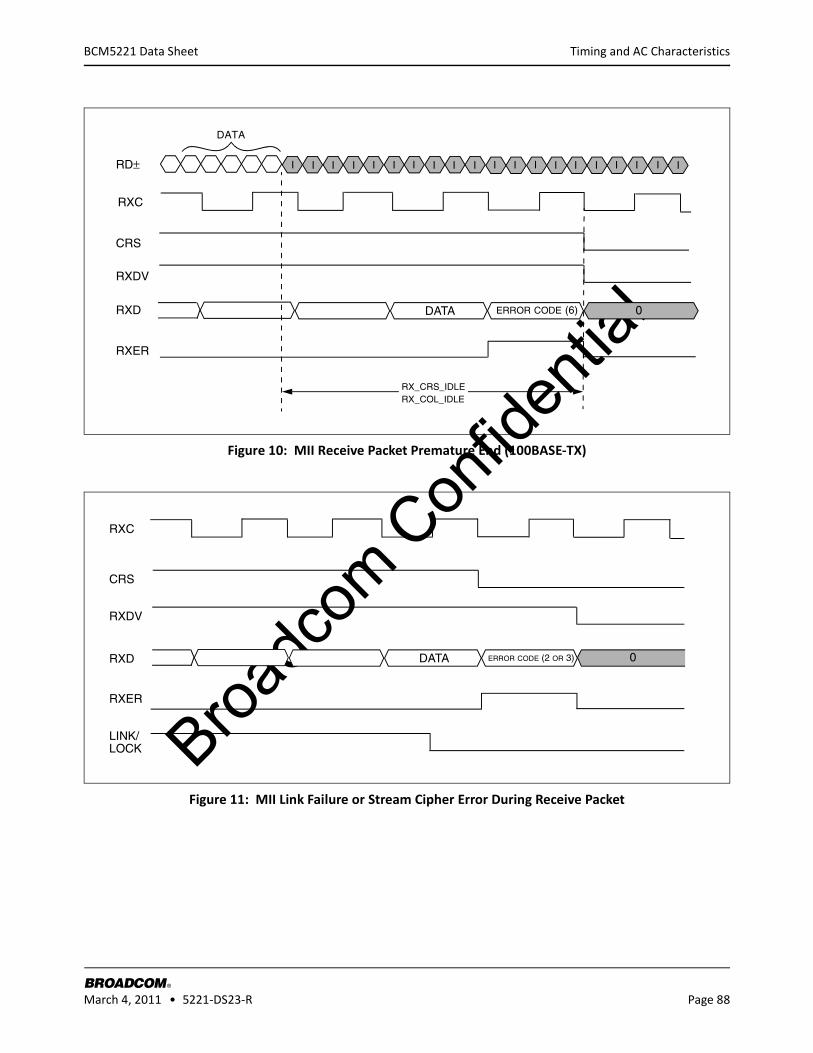
Broadc
om C
onfid
entia
l
Timing and AC Characteristics
BROADCOM March 4, 2011 • 5221-DS23-R Page 88
®
BCM5221 Data Sheet
Figure 10: MII Receive Packet Premature End (100BASE-TX)
Figure 11: MII Link Failure or Stream Cipher Error During Receive Packet
DATA
I
RXDV
RXD
RD±
RXC
CRS
I I I III I I I III III I I III
DATA ERROR CODE (6)
RX_CRS_IDLERX_COL_IDLE
RXER
0
RXDV
RXD
RXC
CRS
DATA ERROR CODE (2 OR 3)
RXER
LINK/ LOCK
0
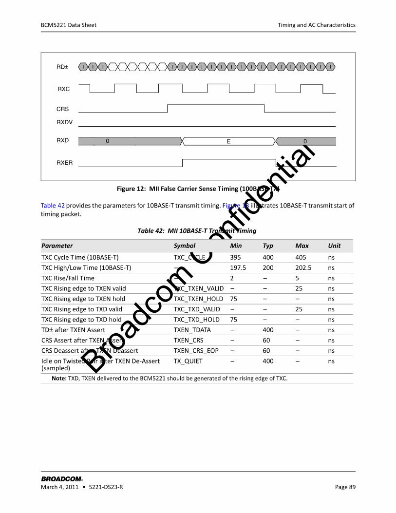
Broadc
om C
onfid
entia
l
Timing and AC Characteristics
BROADCOM March 4, 2011 • 5221-DS23-R Page 89
®
BCM5221 Data Sheet
Figure 12: MII False Carrier Sense Timing (100BASE-TX)
Table 42 provides the parameters for 10BASE-T transmit timing. Figure 13 illustrates 10BASE-T transmit start of timing packet.
Table 42: MII 10BASE-T Transmit Timing
Parameter Symbol Min Typ Max Unit
TXC Cycle Time (10BASE-T) TXC_CYCLE 395 400 405 ns
TXC High/Low Time (10BASE-T) – 197.5 200 202.5 ns
TXC Rise/Fall Time – 2 – 5 ns
TXC Rising edge to TXEN valid TXC_TXEN_VALID – – 25 ns
TXC Rising edge to TXEN hold TXC_TXEN_HOLD 75 – – ns
TXC Rising edge to TXD valid TXC_TXD_VALID – – 25 ns
TXC Rising edge to TXD hold TXC_TXD_HOLD 75 – – ns
TD± after TXEN Assert TXEN_TDATA – 400 – ns
CRS Assert after TXEN Assert TXEN_CRS – 60 – ns
CRS Deassert after TXEN Deassert TXEN_CRS_EOP – 60 – ns
Idle on Twisted Pair after TXEN De-Assert (sampled)
TX_QUIET – 400 – ns
Note: TXD, TXEN delivered to the BCM5221 should be generated of the rising edge of TXC.
0
RXDV
RXD
RD±
RXC
CRS
RXER
0E
I I I III I I I III I III IIII
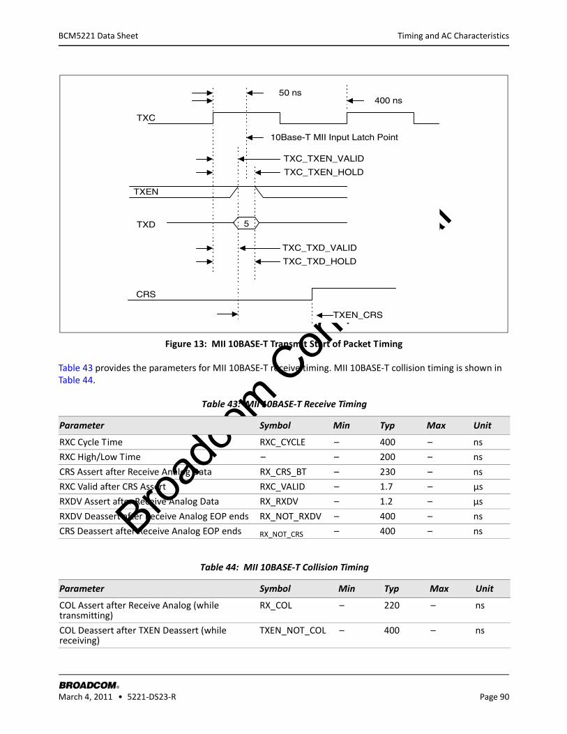
Broadc
om C
onfid
entia
l
Timing and AC Characteristics
BROADCOM March 4, 2011 • 5221-DS23-R Page 90
®
BCM5221 Data Sheet
Figure 13: MII 10BASE-T Transmit Start of Packet Timing
Table 43 provides the parameters for MII 10BASE-T receive timing. MII 10BASE-T collision timing is shown in Table 44.
Table 43: MII 10BASE-T Receive Timing
Parameter Symbol Min Typ Max Unit
RXC Cycle Time RXC_CYCLE – 400 – ns
RXC High/Low Time – – 200 – ns
CRS Assert after Receive Analog Data RX_CRS_BT – 230 – ns
RXC Valid after CRS Assert RXC_VALID – 1.7 – µs
RXDV Assert after Receive Analog Data RX_RXDV – 1.2 – µs
RXDV Deassert after Receive Analog EOP ends RX_NOT_RXDV – 400 – ns
CRS Deassert after Receive Analog EOP ends RX_NOT_CRS – 400 – ns
Table 44: MII 10BASE-T Collision Timing
Parameter Symbol Min Typ Max Unit
COL Assert after Receive Analog (while transmitting)
RX_COL – 220 – ns
COL Deassert after TXEN Deassert (while receiving)
TXEN_NOT_COL – 400 – ns
TXC
TXEN
TXC_TXEN_VALID
TXC_TXEN_HOLD
10Base-T MII Input Latch Point
50 ns
5TXD
CRS
TXEN_CRS
TXC_TXD_HOLD
TXC_TXD_VALID
400 ns
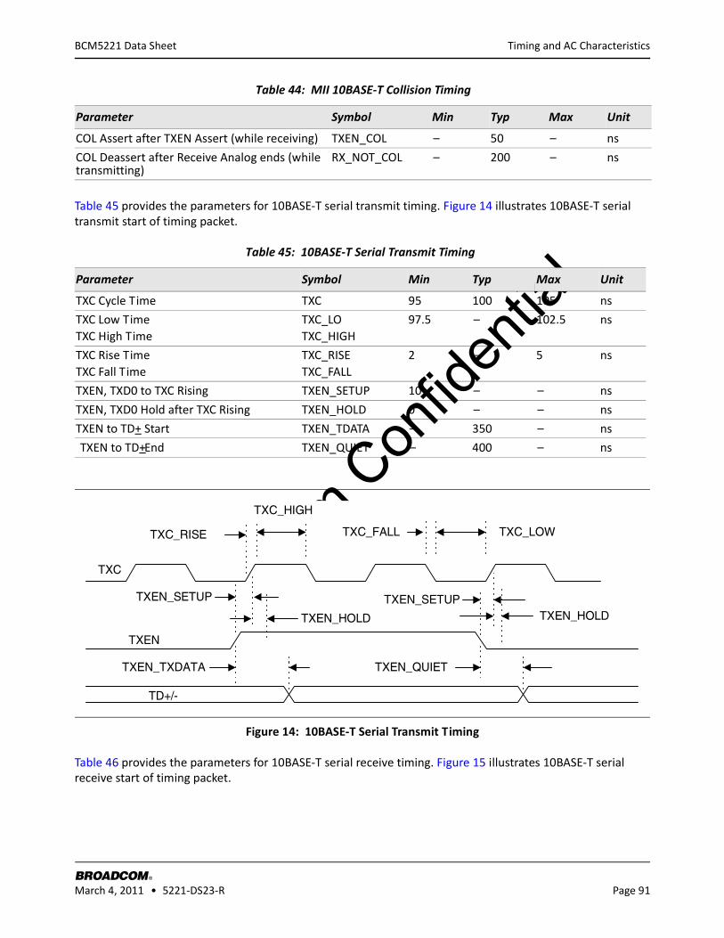
Broadc
om C
onfid
entia
l
Timing and AC Characteristics
BROADCOM March 4, 2011 • 5221-DS23-R Page 91
®
BCM5221 Data Sheet
Table 45 provides the parameters for 10BASE-T serial transmit timing. Figure 14 illustrates 10BASE-T serial transmit start of timing packet.
Figure 14: 10BASE-T Serial Transmit Timing
Table 46 provides the parameters for 10BASE-T serial receive timing. Figure 15 illustrates 10BASE-T serial receive start of timing packet.
COL Assert after TXEN Assert (while receiving) TXEN_COL – 50 – ns
COL Deassert after Receive Analog ends (while transmitting)
RX_NOT_COL – 200 – ns
Table 45: 10BASE-T Serial Transmit Timing
Parameter Symbol Min Typ Max Unit
TXC Cycle Time TXC 95 100 105 ns
TXC Low TimeTXC High Time
TXC_LOTXC_HIGH
97.5 – 102.5 ns
TXC Rise TimeTXC Fall Time
TXC_RISETXC_FALL
2 – 5 ns
TXEN, TXD0 to TXC Rising TXEN_SETUP 10 – – ns
TXEN, TXD0 Hold after TXC Rising TXEN_HOLD 0 – – ns
TXEN to TD+ Start TXEN_TDATA – 350 – ns
TXEN to TD+ End TXEN_QUIET – 400 – ns
Table 44: MII 10BASE-T Collision Timing
Parameter Symbol Min Typ Max Unit
TXC_LOW
TXC_HIGH
TXC_RISE TXC_FALL
TXC
TXEN
TXEN_SETUP
TXEN_HOLD
TXEN_QUIETTXEN_TXDATA
TXEN_SETUPTXEN_HOLD
TD+/-
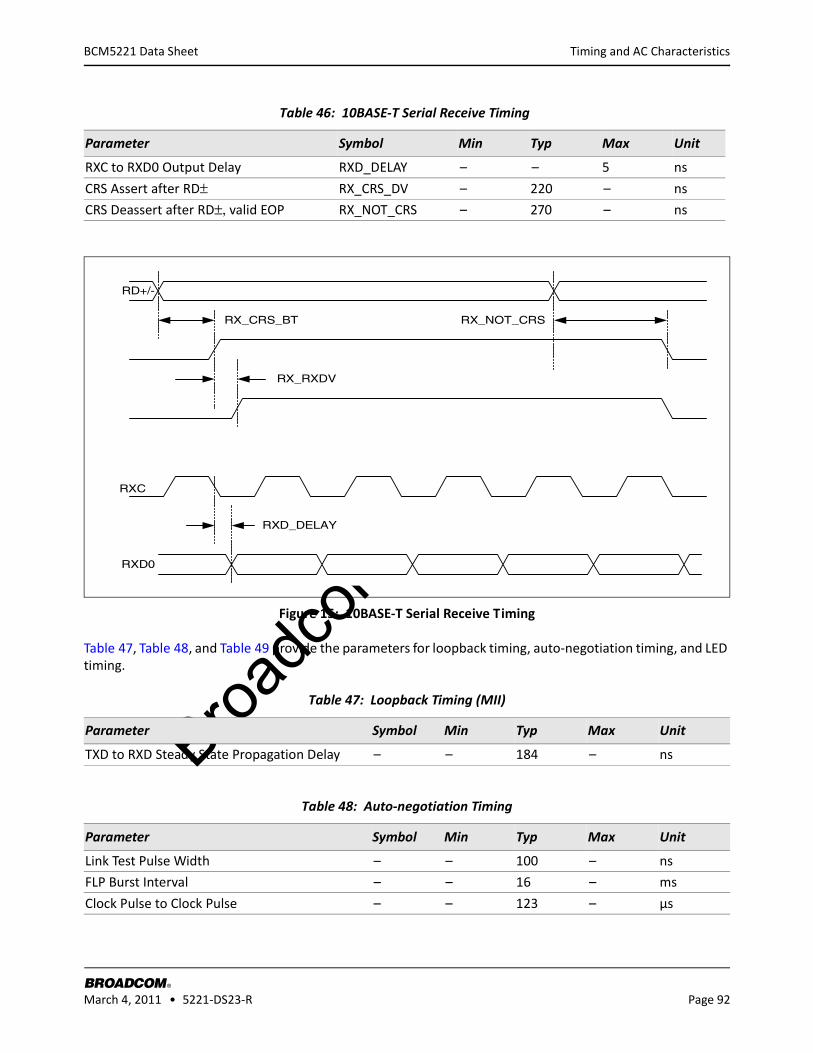
Broadc
om C
onfid
entia
l
Timing and AC Characteristics
BROADCOM March 4, 2011 • 5221-DS23-R Page 92
®
BCM5221 Data Sheet
Figure 15: 10BASE-T Serial Receive Timing
Table 47, Table 48, and Table 49 provide the parameters for loopback timing, auto-negotiation timing, and LED timing.
Table 46: 10BASE-T Serial Receive Timing
Parameter Symbol Min Typ Max Unit
RXC to RXD0 Output Delay RXD_DELAY – – 5 ns
CRS Assert after RD± RX_CRS_DV – 220 – ns
CRS Deassert after RD±, valid EOP RX_NOT_CRS – 270 – ns
Table 47: Loopback Timing (MII)
Parameter Symbol Min Typ Max Unit
TXD to RXD Steady State Propagation Delay – – 184 – ns
Table 48: Auto-negotiation Timing
Parameter Symbol Min Typ Max Unit
Link Test Pulse Width – – 100 – ns
FLP Burst Interval – – 16 – ms
Clock Pulse to Clock Pulse – – 123 – µs
RXC
RXD0
RXD_DELAY
RD+/-
RX_CRS_BT
RX_RXDV
RX_NOT_CRS
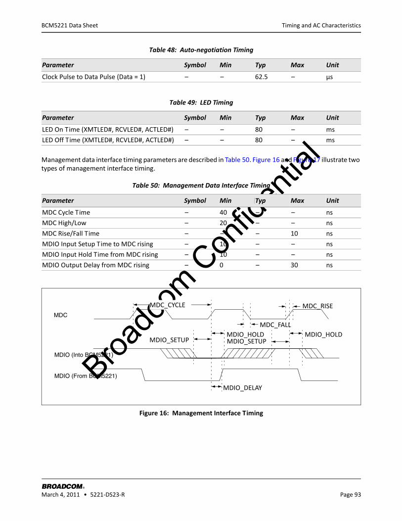
Broadc
om C
onfid
entia
l
Timing and AC Characteristics
BROADCOM March 4, 2011 • 5221-DS23-R Page 93
®
BCM5221 Data Sheet
Management data interface timing parameters are described in Table 50. Figure 16 and Figure 17 illustrate two types of management interface timing.
Figure 16: Management Interface Timing
Clock Pulse to Data Pulse (Data = 1) – – 62.5 – µs
Table 49: LED Timing
Parameter Symbol Min Typ Max Unit
LED On Time (XMTLED#, RCVLED#, ACTLED#) – – 80 – ms
LED Off Time (XMTLED#, RCVLED#, ACTLED#) – – 80 – ms
Table 50: Management Data Interface Timing
Parameter Symbol Min Typ Max Unit
MDC Cycle Time – 40 – – ns
MDC High/Low – 20 – – ns
MDC Rise/Fall Time – – – 10 ns
MDIO Input Setup Time to MDC rising – 10 – – ns
MDIO Input Hold Time from MDC rising – 10 – – ns
MDIO Output Delay from MDC rising – 0 – 30 ns
Table 48: Auto-negotiation Timing
Parameter Symbol Min Typ Max Unit
MDIO (From BCM5221)
MDC
MDC_FALLMDIO_HOLD
MDIO_SETUP
MDC_RISEMDC_CYCLE
MDIO_SETUPMDIO_HOLD
MDIO_DELAY
MDIO (Into BCM5221)
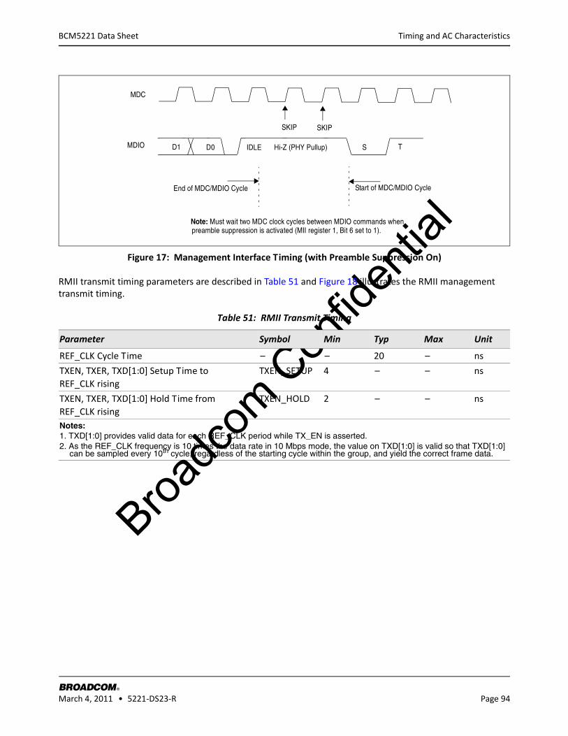
Broadc
om C
onfid
entia
l
Timing and AC Characteristics
BROADCOM March 4, 2011 • 5221-DS23-R Page 94
®
BCM5221 Data Sheet
Figure 17: Management Interface Timing (with Preamble Suppression On)
RMII transmit timing parameters are described in Table 51 and Figure 18 illustrates the RMII management transmit timing.
Table 51: RMII Transmit Timing
Parameter Symbol Min Typ Max Unit
REF_CLK Cycle Time – – 20 – ns
TXEN, TXER, TXD[1:0] Setup Time toREF_CLK rising
TXEN_SETUP 4 – – ns
TXEN, TXER, TXD[1:0] Hold Time fromREF_CLK rising
TXEN_HOLD 2 – – ns
Notes:1. TXD[1:0] provides valid data for each REF_CLK period while TX_EN is asserted.2. As the REF_CLK frequency is 10 times the data rate in 10 Mbps mode, the value on TXD[1:0] is valid so that TXD[1:0]
can be sampled every 10th cycle, regardless of the starting cycle within the group, and yield the correct frame data.
MDC
SKIP SKIP
D0D1 Hi-Z (PHY Pullup)IDLE S TMDIO
Start of MDC/MDIO CycleEnd of MDC/MDIO Cycle
Note: Must wait two MDC clock cycles between MDIO commands whenpreamble suppression is activated (MII register 1, Bit 6 set to 1).
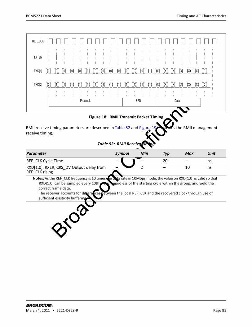
Broadc
om C
onfid
entia
l
Timing and AC Characteristics
BROADCOM March 4, 2011 • 5221-DS23-R Page 95
®
BCM5221 Data Sheet
Figure 18: RMII Transmit Packet Timing
RMII receive timing parameters are described in Table 52 and Figure 19 illustrates the RMII management receive timing.
Table 52: RMII Receive Timing
Parameter Symbol Min Typ Max Unit
REF_CLK Cycle Time – – 20 – ns
RXD[1:0], RXER, CRS_DV Output delay from REF_CLK rising
– 2 – 10 ns
Notes: As the REF_CLK frequency is 10 times the data rate in 10Mbps mode, the value on RXD[1:0] is valid so that RXD[1:0] can be sampled every 10th cycle, regardless of the starting cycle within the group, and yield the correct frame data. The receiver accounts for differences between the local REF_CLK and the recovered clock through use of sufficient elasticity buffering.
00000
0 0
0TXD[1]
TXD[0]
TX_EN
REF_CLK
1
111 1 1 1 1 1 1 1 1 1 1 X X X XX X
XXXXXX0 0 0 0 0 0 0 0
Preamble DataSFD
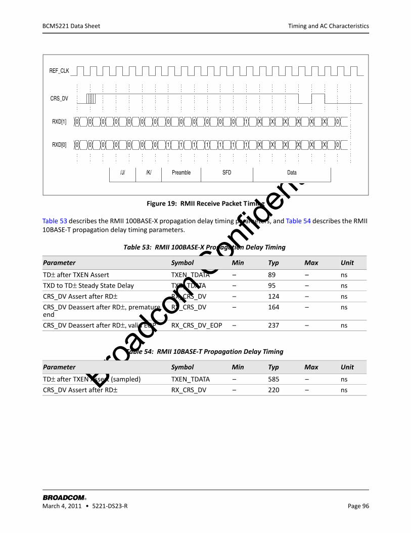
Broadc
om C
onfid
entia
l
Timing and AC Characteristics
BROADCOM March 4, 2011 • 5221-DS23-R Page 96
®
BCM5221 Data Sheet
Figure 19: RMII Receive Packet Timing
Table 53 describes the RMII 100BASE-X propagation delay timing parameters, and Table 54 describes the RMII 10BASE-T propagation delay timing parameters.
Table 53: RMII 100BASE-X Propagation Delay Timing
Parameter Symbol Min Typ Max Unit
TD± after TXEN Assert TXEN_TDATA – 89 – ns
TXD to TD± Steady State Delay TXD_TDATA – 95 – ns
CRS_DV Assert after RD± RX_CRS_DV – 124 – ns
CRS_DV Deassert after RD±, premature end
RX_CRS_DV – 164 – ns
CRS_DV Deassert after RD±, valid EOP RX_CRS_DV_EOP – 237 – ns
Table 54: RMII 10BASE-T Propagation Delay Timing
Parameter Symbol Min Typ Max Unit
TD± after TXEN Assert (sampled) TXEN_TDATA – 585 – ns
CRS_DV Assert after RD± RX_CRS_DV – 220 – ns
/J/ /K/ Preamble SFD Data
0
1
000 000000000
0 0 0 0 0 0 0 1 1 1 1 1 1 X X X X X 0
0
X
X X X X XX1RXD[1]
RXD[0]
CRS_DV
REF_CLK
Broadc
om C
onfid
entia
l
Electrical Characteristics
BROADCOM March 4, 2011 • 5221-DS23-R Page 97
®
BCM5221 Data Sheet
Section 7: Electrical Characteristics
Table 55 provides the absolute maximum ratings for the BCM5221. Table 56 shows the recommended operating conditions for the BCM5221. Table 57 gives the electrical characteristics of the BCM5221.
. Table 55: Absolute Maximum Ratings
Symbols Parameters Min Max Units
VDD Supply voltage REGDVDD, REGAVDD, OVDD GND − 0.3 3.60 V
DVDD, AVDD, BIASVDD GND − 0.3 2.75 V
TD+, TD – , RD+, RD – – 6.53 V
VI Input voltage GND − 0.3 OVDD + 0.3 V
II Input current – ±10 mA
TSTG Storage temperature –40 +125 °CNote: These specifications indicate levels where permanent damage to the device may occur. Functional
operation is not guaranteed under these conditions. Operation at absolute maximum conditions for extended periods may adversely affect long-term reliability of the device
Table 56: Recommended Operating Conditions
Sym Parameter Pin Operating Mode Min Max Units
VDD Supply voltage BCM5221
REGDVDD, REGAVDD – 3.00 3.60 V
OVDD – 2.375 3.60 V
VIH High-levelinput voltage
All digital inputs, at 3.3V OVDDAll digital inputs, at 2.5V OVDD
– 2.01.8
OVDDOVDD
VV –
VIL Low-level input voltage
All digital inputs, at 3.3V OVDDAll digital inputs, at 2.5V OVDD
– – 0.80.7
VV
SD± 100BASE-TX – 0.4 V
VIDIFF Differential input voltage
RD±,SD± 100BASE-FX 150 – mV
VICM Common mode input voltage
RD± 100BASE-TX 1.85 2.05 V
RD±,SD± 100BASE-FX 1.85 2.05 V
TA Ambient operating temperature –40 85 °C
Table 57: Electrical Characteristics
Sym Parameter Pins Conditions Min Typ Max Units
IDD Supply current AVDD, DVDD, OVDD 100BASE-TX – 110 – mA
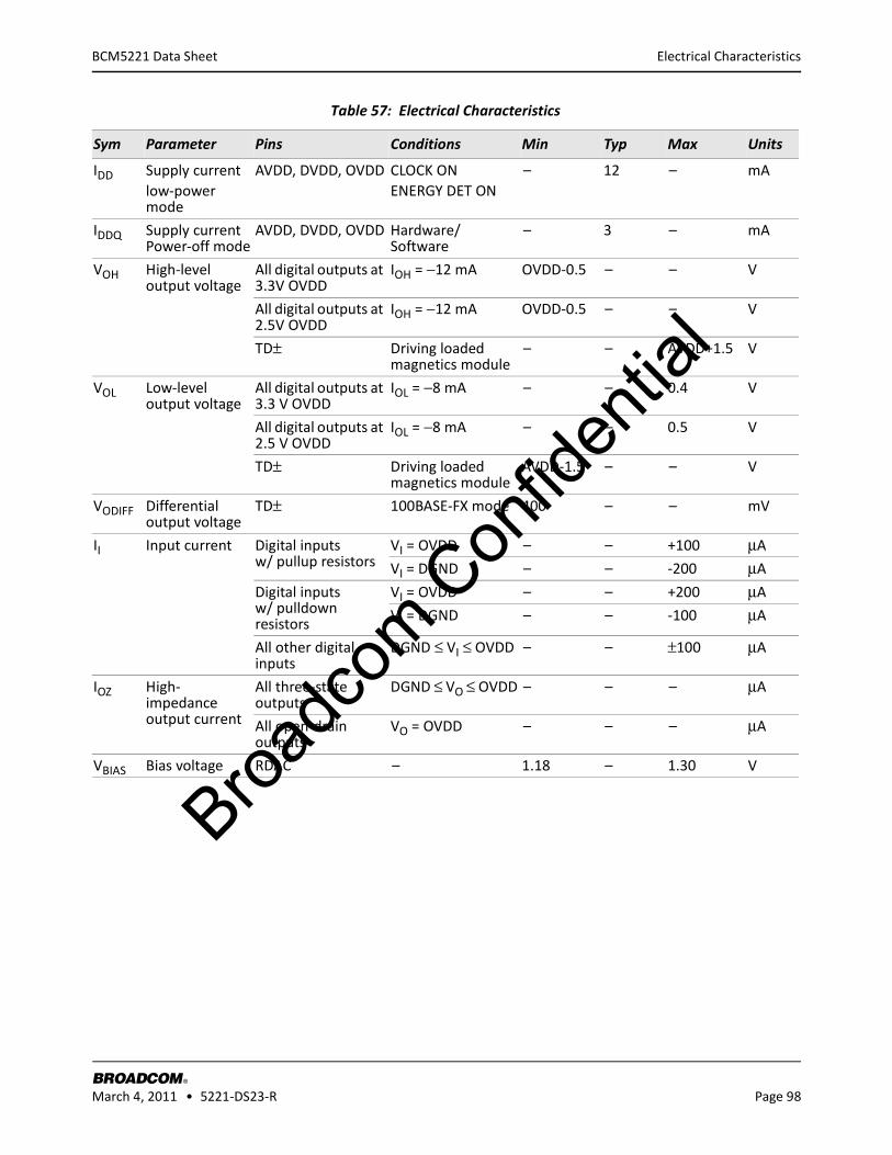
Broadc
om C
onfid
entia
l
Electrical Characteristics
BROADCOM March 4, 2011 • 5221-DS23-R Page 98
®
BCM5221 Data Sheet
IDD Supply currentlow-power mode
AVDD, DVDD, OVDD CLOCK ONENERGY DET ON
– 12 – mA
IDDQ Supply current Power-off mode
AVDD, DVDD, OVDD Hardware/Software
– 3 – mA
VOH High-level output voltage
All digital outputs at 3.3V OVDD
IOH = −12 mA OVDD-0.5 – – V
All digital outputs at 2.5V OVDD
IOH = −12 mA OVDD-0.5 – – V
TD± Driving loaded magnetics module
– – AVDD+1.5 V
VOL Low-level output voltage
All digital outputs at 3.3 V OVDD
IOL = −8 mA – – 0.4 V
All digital outputs at 2.5 V OVDD
IOL = −8 mA – – 0.5 V
TD± Driving loaded magnetics module
AVDD-1.5 – – V
VODIFF Differential output voltage
TD± 100BASE-FX mode 400 – – mV
II Input current Digital inputs w/ pullup resistors
VI = OVDD – – +100 μA
VI = DGND – – -200 μA
Digital inputs w/ pulldown resistors
VI = OVDD – – +200 μA
VI = DGND – – -100 μA
All other digital inputs
DGND ≤ VI ≤ OVDD – – ±100 μA
IOZ High-impedance output current
All three-state outputs
DGND ≤ VO ≤ OVDD – – – μA
All open-drain outputs
VO = OVDD – – – μA
VBIAS Bias voltage RDAC – 1.18 – 1.30 V
Table 57: Electrical Characteristics
Sym Parameter Pins Conditions Min Typ Max Units
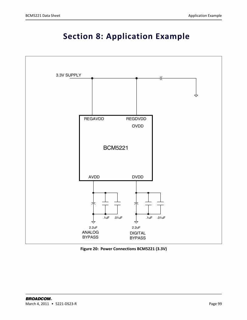
Broadc
om C
onfid
entia
l
Application Example
BROADCOM March 4, 2011 • 5221-DS23-R Page 99
®
BCM5221 Data Sheet
Section 8: Application Example
Figure 20: Power Connections BCM5221 (3.3V)
BCM5221
DIGITALBYPASS
ANALOGBYPASS
REGAVDD REGDVDD
AVDD DVDD
OVDD
.1uF
2.2uF
.01uF
3.3V SUPPLY
.1uF
2.2uF
.01uF
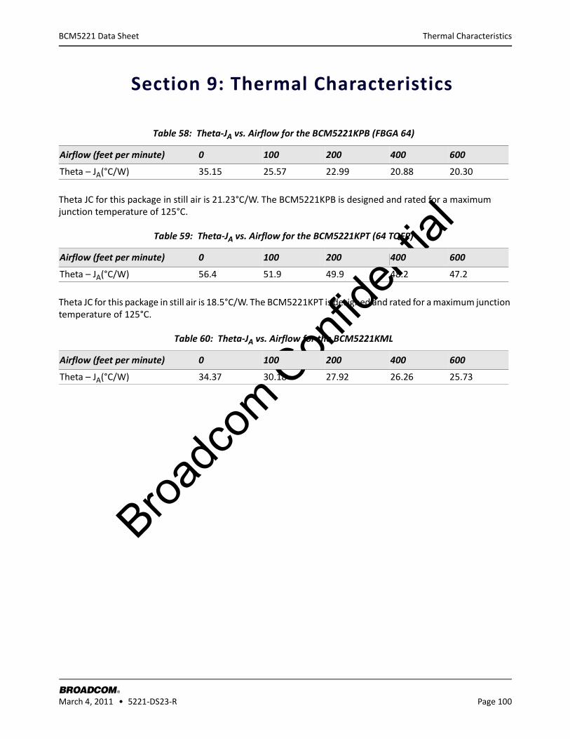
Broadc
om C
onfid
entia
l
Thermal Characteristics
BROADCOM March 4, 2011 • 5221-DS23-R Page 100
®
BCM5221 Data Sheet
Section 9: Thermal Characteristics
Theta JC for this package in still air is 21.23°C/W. The BCM5221KPB is designed and rated for a maximum junction temperature of 125°C.
Theta JC for this package in still air is 18.5°C/W. The BCM5221KPT is designed and rated for a maximum junction temperature of 125°C.
Table 58: Theta-JA vs. Airflow for the BCM5221KPB (FBGA 64)
Airflow (feet per minute) 0 100 200 400 600
Theta – JA(°C/W) 35.15 25.57 22.99 20.88 20.30
Table 59: Theta-JA vs. Airflow for the BCM5221KPT (64 TQFP)
Airflow (feet per minute) 0 100 200 400 600
Theta – JA(°C/W) 56.4 51.9 49.9 48.2 47.2
Table 60: Theta-JA vs. Airflow for the BCM5221KML
Airflow (feet per minute) 0 100 200 400 600
Theta – JA(°C/W) 34.37 30.18 27.92 26.26 25.73
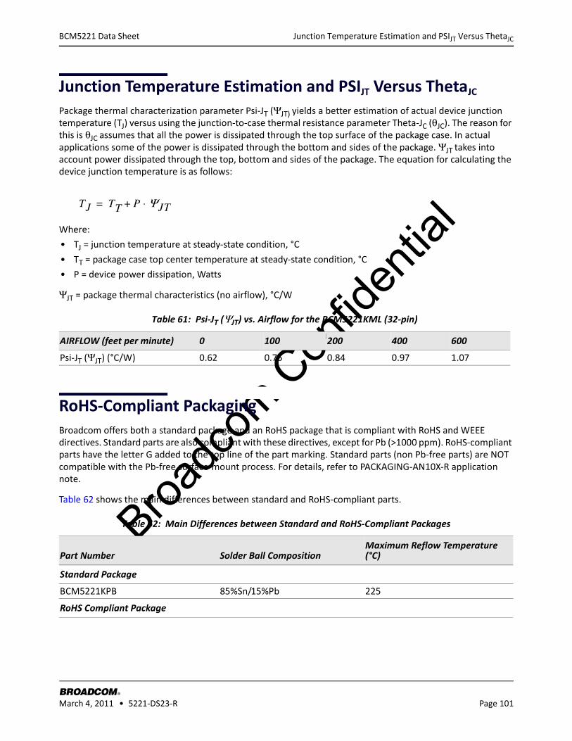
Broadc
om C
onfid
entia
l
Junction Temperature Estimation and PSIJT Versus ThetaJC
BROADCOM March 4, 2011 • 5221-DS23-R Page 101
®
BCM5221 Data Sheet
Junction Temperature Estimation and PSIJT Versus ThetaJC
Package thermal characterization parameter Psi-JT (ΨJT) yields a better estimation of actual device junction temperature (TJ) versus using the junction-to-case thermal resistance parameter Theta-JC (θJC). The reason for this is θJC assumes that all the power is dissipated through the top surface of the package case. In actual applications some of the power is dissipated through the bottom and sides of the package. ΨJT takes into account power dissipated through the top, bottom and sides of the package. The equation for calculating the device junction temperature is as follows:
Where:
• TJ = junction temperature at steady-state condition, °C
• TT = package case top center temperature at steady-state condition, °C
• P = device power dissipation, Watts
ΨJT = package thermal characteristics (no airflow), °C/W
RoHS-Compliant PackagingBroadcom offers both a standard package and an RoHS package that is compliant with RoHS and WEEE directives. Standard parts are also compliant with these directives, except for Pb (>1000 ppm). RoHS-compliant parts have the letter G added to the top line of the part marking. Standard parts (non Pb-free parts) are NOT compatible with the Pb-free surface-mount process. For details, refer to PACKAGING-AN10X-R application note.
Table 62 shows the main differences between standard and RoHS-compliant parts.
Table 61: Psi-JT (ΨJT) vs. Airflow for the BCM5221KML (32-pin)
AIRFLOW (feet per minute) 0 100 200 400 600
Psi-JT (ΨJT) (°C/W) 0.62 0.75 0.84 0.97 1.07
Table 62: Main Differences between Standard and RoHS-Compliant Packages
Part Number Solder Ball CompositionMaximum Reflow Temperature (°C)
Standard Package
BCM5221KPB 85%Sn/15%Pb 225
RoHS Compliant Package
TJ TT P ΨJT⋅+=

Broadc
om C
onfid
entia
l
RoHS-Compliant Packaging
BROADCOM March 4, 2011 • 5221-DS23-R Page 102
®
BCM5221 Data Sheet
BCM5221A4KPTGBCM5221A4KMLGBCM5221A4IMLG
100%Sn 255
Table 62: Main Differences between Standard and RoHS-Compliant Packages
Part Number Solder Ball CompositionMaximum Reflow Temperature (°C)
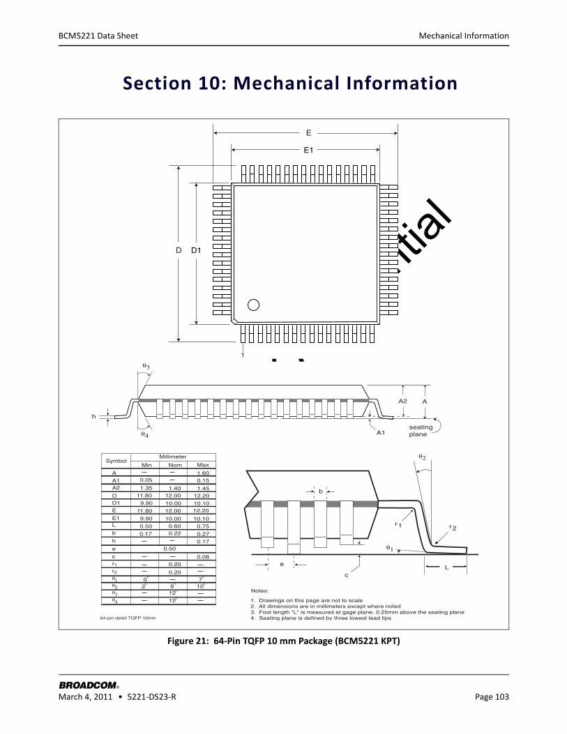
Broadc
om C
onfid
entia
l
Mechanical Information
BROADCOM March 4, 2011 • 5221-DS23-R Page 103
®
BCM5221 Data Sheet
Section 10: Mechanical Information
Figure 21: 64-Pin TQFP 10 mm Package (BCM5221 KPT)
seatingplane
A
A1
A2
L
b
e
r1
θ2
r2
θ1
c
1. Drawings on this page are not to scale2. All dimensions are in millimeters except where noted3. Foot length "L" is measured at gage plane, 0.25mm above the seating plane4. Seating plane is defined by three lowest lead tips64-pin detail TQFP 10mm
θ3
θ4
h
MillimeterSymbol
Min Nom Max
A
A1A2
DD1
E
E1L
e
b
c
0.05
1.35
11.80
9.90
11.80
0.50
0.50
0.17 0.22 0.27
0.60 0.75
12.00 12.2010.00 10.10
12.00 12.20
1.40 1.45
0.151.60
0.17h
0.08r
r0.20
0.20
3θ
1θ
2θ
4θ
°2
°0°6
°7
°12
°12
°10Notes:
1
2
9.90 10.00 10.10
D1D
E1
E
1
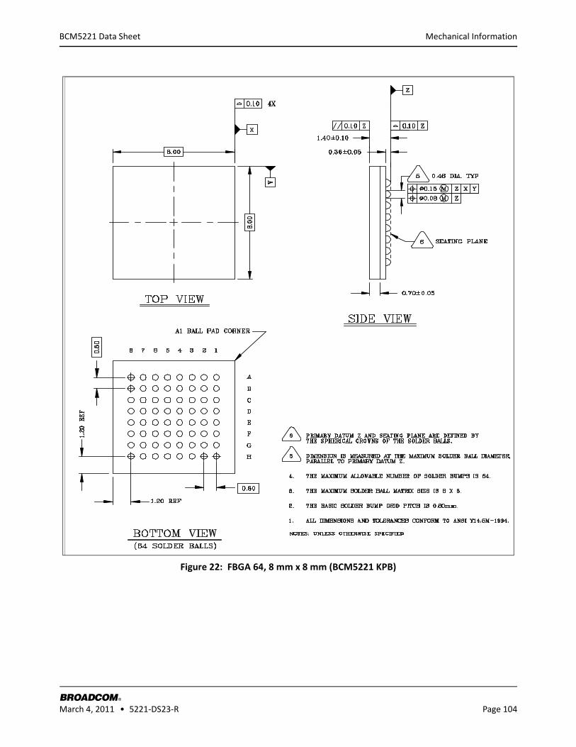
Broadc
om C
onfid
entia
l
Mechanical Information
BROADCOM March 4, 2011 • 5221-DS23-R Page 104
®
BCM5221 Data Sheet
Figure 22: FBGA 64, 8 mm x 8 mm (BCM5221 KPB)
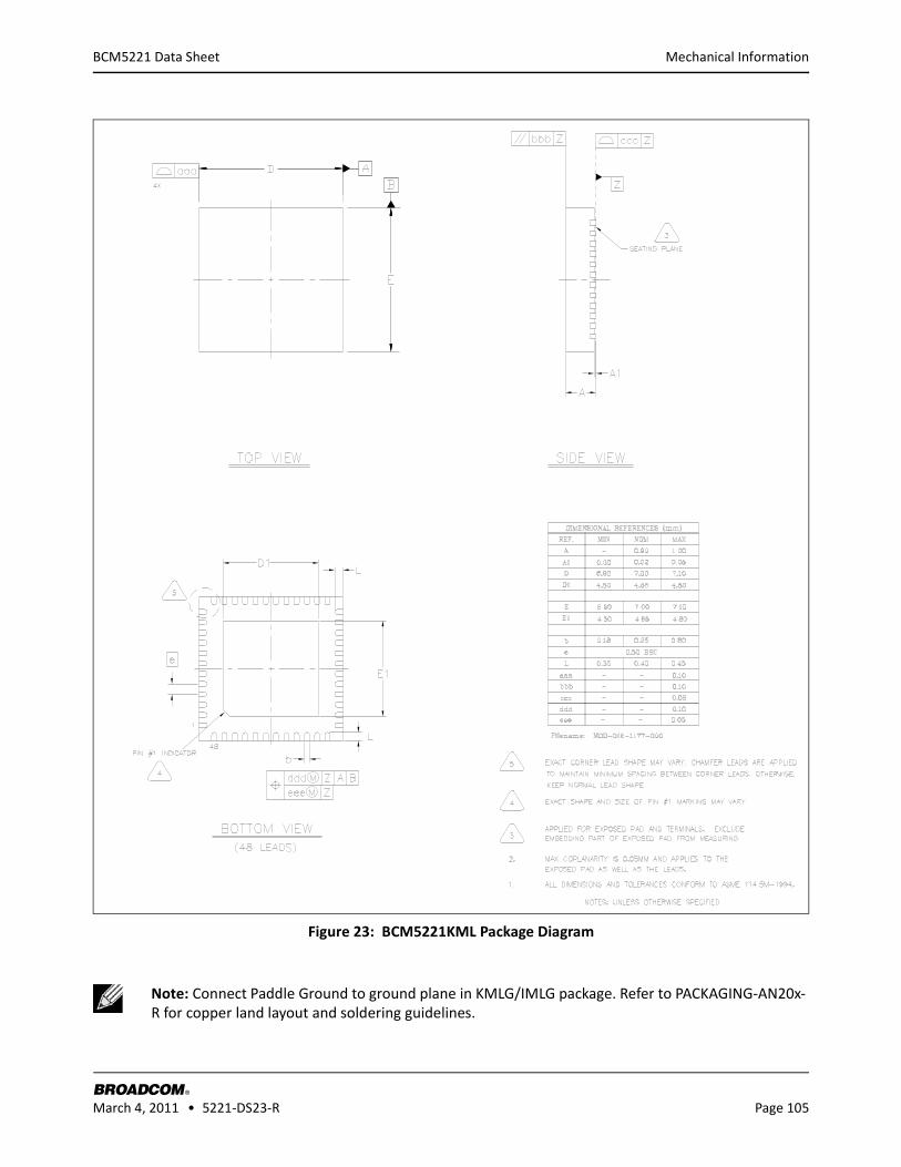
Broadc
om C
onfid
entia
l
Mechanical Information
BROADCOM March 4, 2011 • 5221-DS23-R Page 105
®
BCM5221 Data Sheet
Figure 23: BCM5221KML Package Diagram
Note: Connect Paddle Ground to ground plane in KMLG/IMLG package. Refer to PACKAGING-AN20x-R for copper land layout and soldering guidelines.
Broadc
om C
onfid
entia
l
Ordering Information
BROADCOM March 4, 2011 • 5221-DS23-R Page 106
®
BCM5221 Data Sheet
Section 11: Ordering Information
Part Number Package Ambient Temperature
BCM5221KPB FBGA 64 – 40°C to 85°C
BCM5221A4KPTG 64-TQFP, RoHS 6/6-compliant package – 40°C to 85°C
BCM5221A4KMLG 48-pin KML, RoHS 6/6-compliant package 0°C to 70°C
BCM5221A4IMLG 48-pin KML, RoHS 6/6-compliant package –40°C to 85°C

Broadc
om C
onfid
entia
l
®
Phone: 949-926-5000Fax: 949-926-5203E-mail: [email protected]: www.broadcom.com
BROADCOM CORPORATION5300 California AvenueIrvine, CA 92617© 2011 by BROADCOM CORPORATION. All rights reserved.
5221-DS23-R March 4, 2011
Broadcom® Corporation reserves the right to make changes without further notice to any products or data herein to improve reliability, function, or design.
Information furnished by Broadcom Corporation is believed to be accurate and reliable. However, Broadcom Corporation does not assume any liability arising out of the application or use of this information, nor the application or use of any product or circuit described herein, neither does it convey any license under its patent rights nor the rights of others.
BCM5221 Data Sheet