Bandwidth Extension Techniques for CMOS Amplifiers...
50
1 1 Bandwidth Extension Techniques for CMOS Amplifiers David J. Allstot, Sudip Shekhar, and Jeffrey S. Walling Dept. of Electrical Engineering University of Washington Seattle, WA 98195-2500
Transcript of Bandwidth Extension Techniques for CMOS Amplifiers...
11
Bandwidth Extension Techniques for CMOS Amplifiers
David J. Allstot, Sudip Shekhar, and Jeffrey S. Walling
Dept. of Electrical EngineeringUniversity of WashingtonSeattle, WA 98195-2500
22
Outline
• Motivations: Performance and Low Power (bandwidth α gm α [I]1/2, settling time, rise time)
• Bridged-Shunt Peaking
• Bridged-Shunt-Series Peaking
• Asymmetric T-coil Peaking
• Wideband Amplifiers
• Results
• Conclusions
33
Motivation
• Broad Band Amplifiers
• Ultra Wideband (UWB) Receivers
• Transimpedance Amplifiers (TIAs)
• Pre-drivers and Mux/Demux
Wireless Wireline Optical
WidebandAmplifiers
44
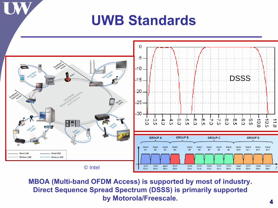
UWB Standards
DSSS
MBOA (Multi-band OFDM Access) is supported by most of industry. Direct Sequence Spread Spectrum (DSSS) is primarily supported
by Motorola/Freescale.
© Intel
55
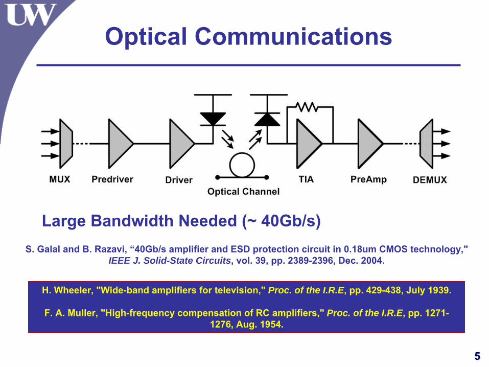
Optical Communications
Large Bandwidth Needed (~ 40Gb/s)S. Galal and B. Razavi, “40Gb/s amplifier and ESD protection circuit in 0.18um CMOS technology,"
IEEE J. Solid-State Circuits, vol. 39, pp. 2389-2396, Dec. 2004.
H. Wheeler, "Wide-band amplifiers for television," Proc. of the I.R.E, pp. 429-438, July 1939.
F. A. Muller, "High-frequency compensation of RC amplifiers," Proc. of the I.R.E, pp. 1271-1276, Aug. 1954.
66
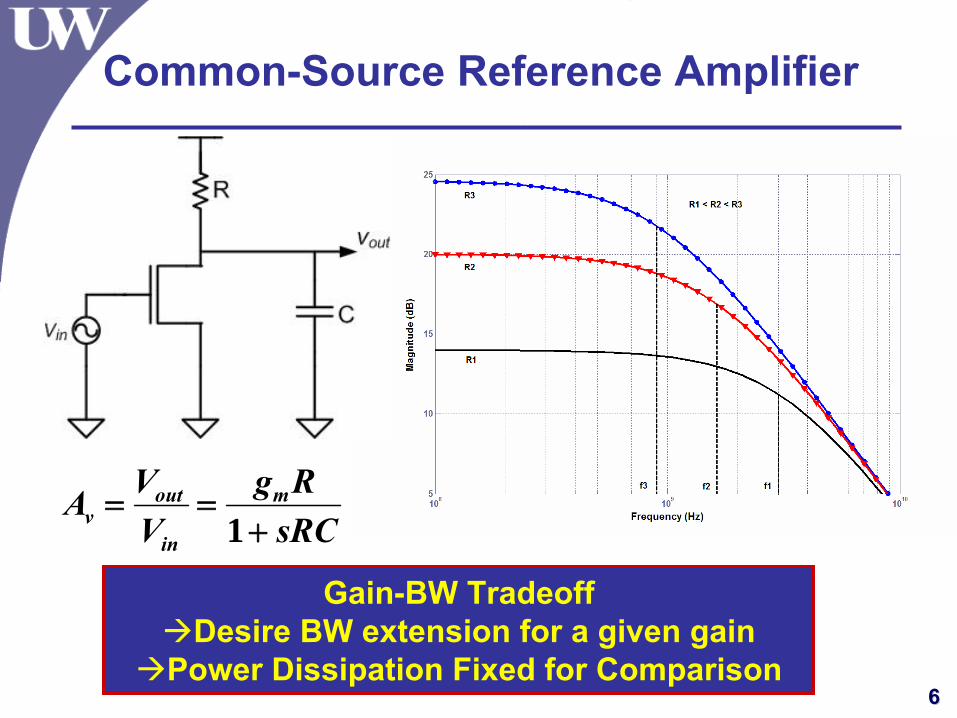
Common-Source Reference Amplifier
sRCRg
VVA m
in
outv +
==1
Gain-BW Tradeoff Desire BW extension for a given gain
Power Dissipation Fixed for Comparison
77
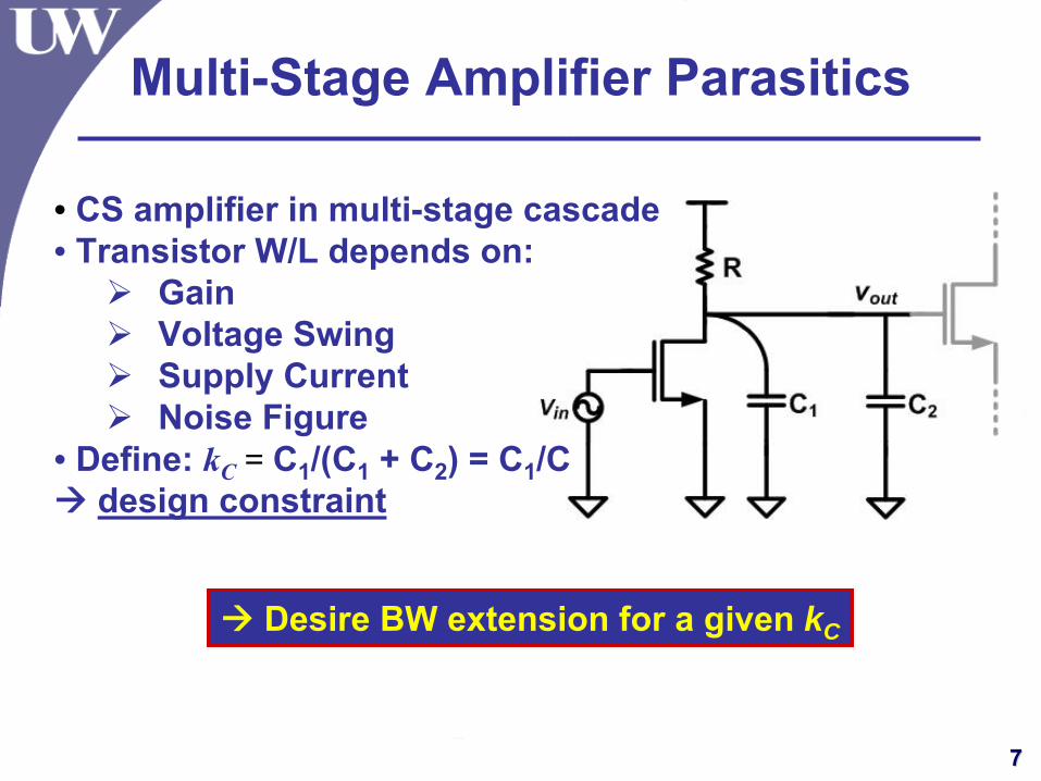
Multi-Stage Amplifier Parasitics
Desire BW extension for a given kC
• CS amplifier in multi-stage cascade• Transistor W/L depends on:
GainVoltage SwingSupply CurrentNoise Figure
• Define: kC = C1/(C1 + C2) = C1/Cdesign constraint
88
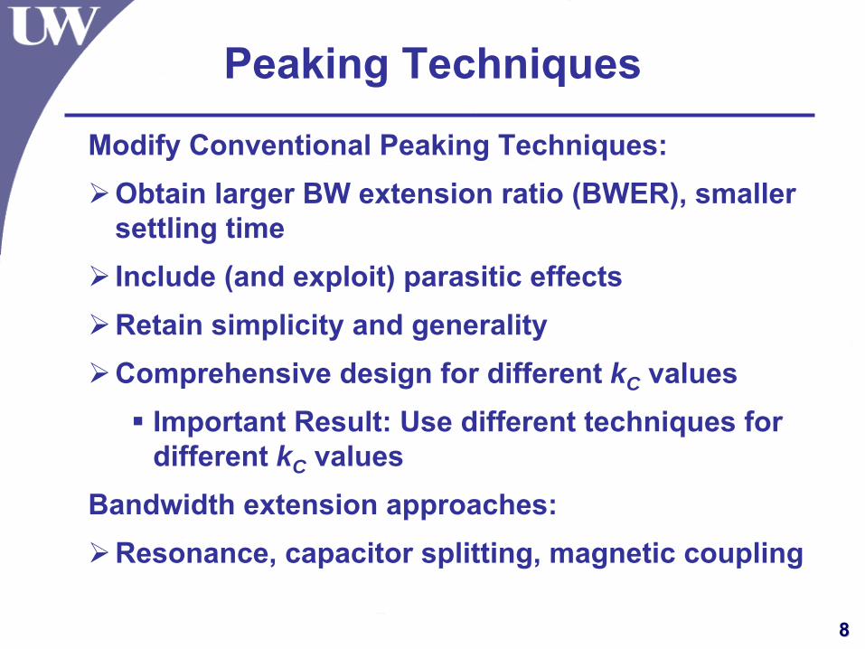
Peaking Techniques
Modify Conventional Peaking Techniques:Obtain larger BW extension ratio (BWER), smaller settling timeInclude (and exploit) parasitic effects Retain simplicity and generality Comprehensive design for different kC values
Important Result: Use different techniques for different kC values
Bandwidth extension approaches:Resonance, capacitor splitting, magnetic coupling
99
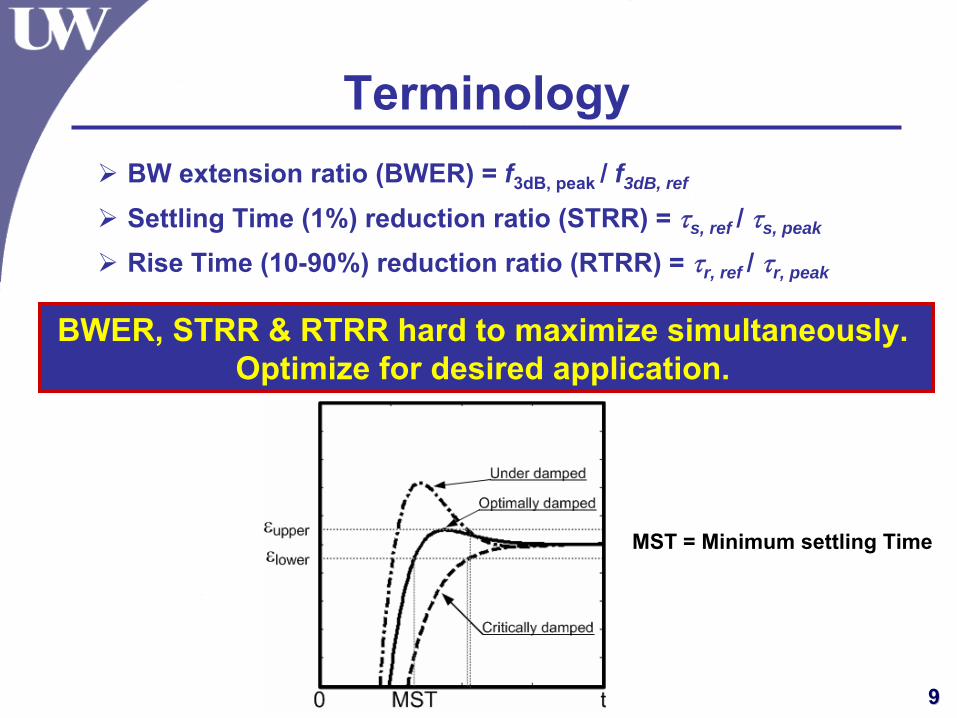
TerminologyBW extension ratio (BWER) = f3dB, peak / f3dB, ref
Settling Time (1%) reduction ratio (STRR) = τs, ref / τs, peak
Rise Time (10-90%) reduction ratio (RTRR) = τr, ref / τr, peak
MST = Minimum settling Time
BWER, STRR & RTRR hard to maximize simultaneously. Optimize for desired application.
1010
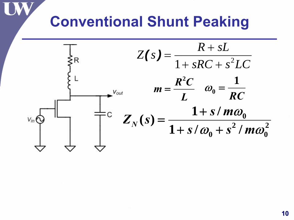
Conventional Shunt Peaking
LCssRCsLRsZ 21 ++
+=)(
20
20
0
//1/1)(
ωωωmss
mssZN +++
=
LCRm
2
=RC1
0 =ω
1111
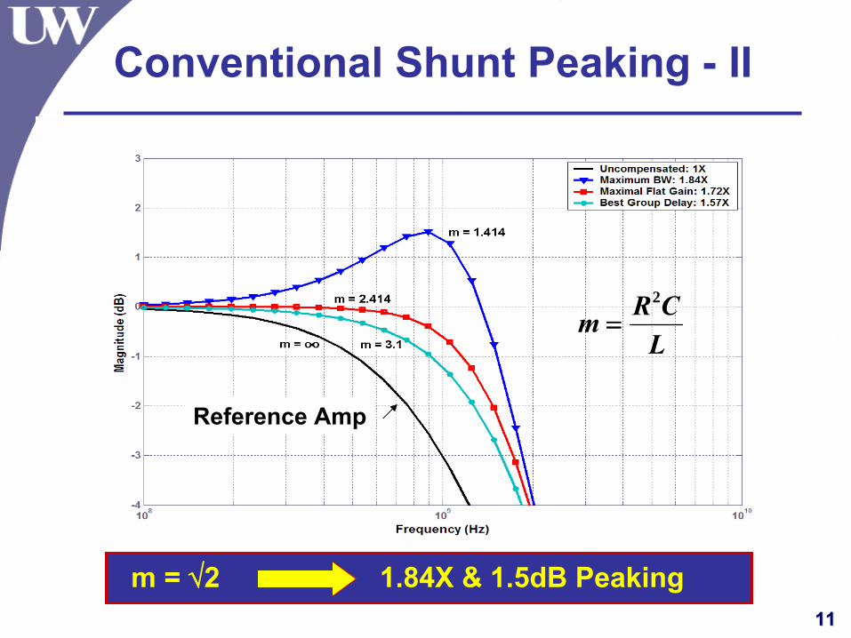
Conventional Shunt Peaking - II
LCRm
2
=
m = √2 1.84X & 1.5dB Peaking
Reference Amp
1212
20
20
0
//1/1)(
ωωωmss
mssZN +++
=
LCRm
2
=RC1
0 =ω
30
3
20
2
0
20
2
0
11
11)(
ωωω
ωωs
mks
mks
smks
msZBB
B
N
⎟⎠⎞
⎜⎝⎛+⎟
⎠⎞
⎜⎝⎛ +++
⎟⎠⎞
⎜⎝⎛+⎟
⎠⎞
⎜⎝⎛+
=
BB
CkC
=
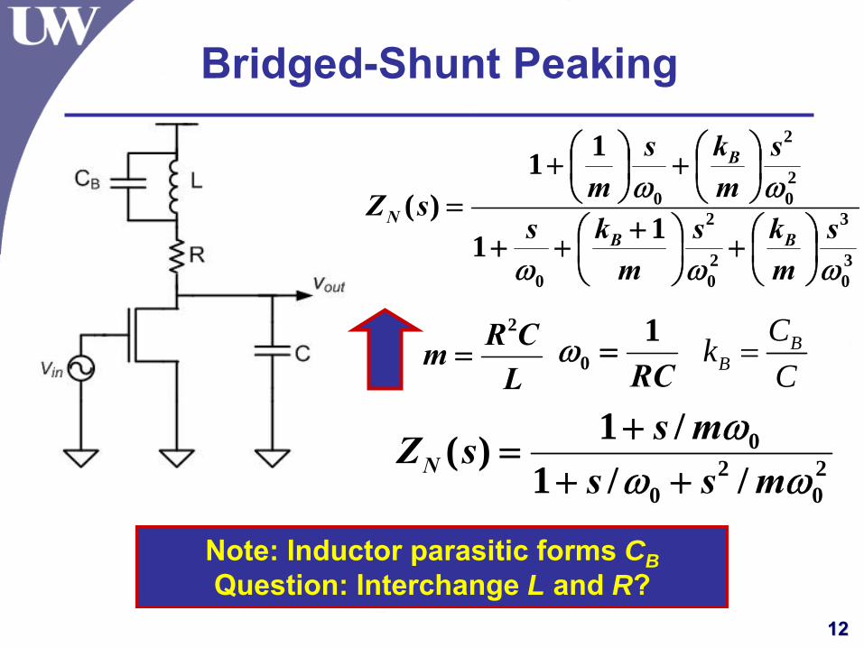
Bridged-Shunt Peaking
Note: Inductor parasitic forms CBQuestion: Interchange L and R?
1313
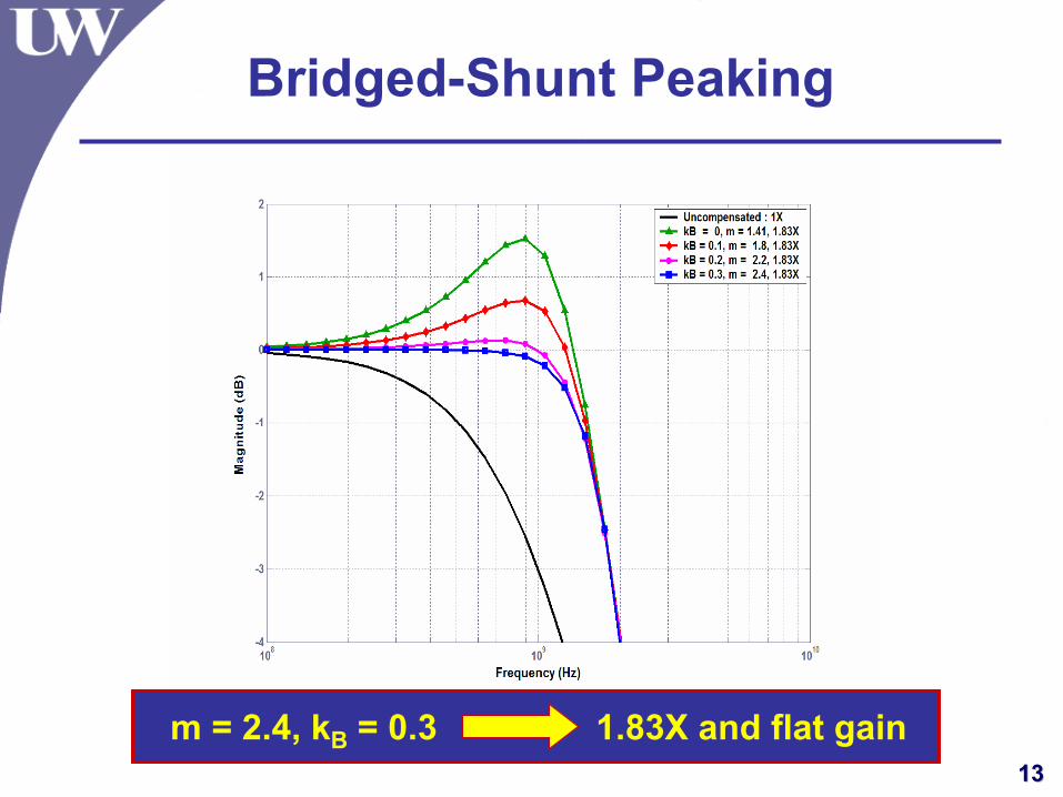
Bridged-Shunt Peaking
m = 2.4, kB = 0.3 1.83X and flat gain
1414
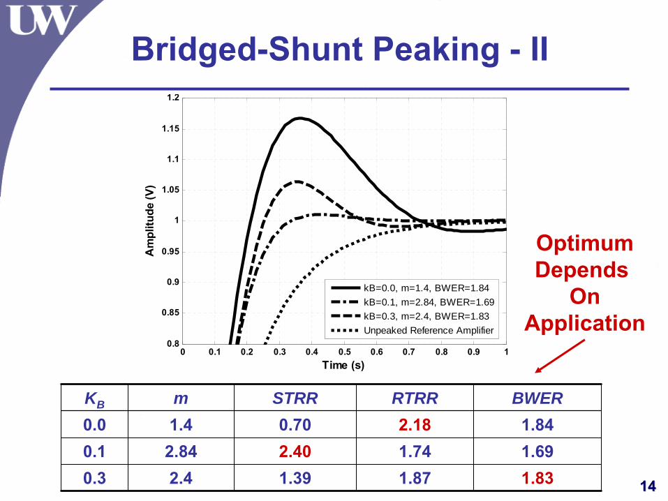
Bridged-Shunt Peaking - II
0 0.1 0.2 0.3 0.4 0.5 0.6 0.7 0.8 0.9 10.8
0.85
0.9
0.95
1
1.05
1.1
1.15
1.2
Time (s)
Am
plitu
de (V
)
kB=0.0, m=1.4, BWER=1.84kB=0.1, m=2.84, BWER=1.69kB=0.3, m=2.4, BWER=1.83Unpeaked Reference Amplifier
1.831.871.392.40.31.691.742.402.840.11.842.180.701.40.0
BWERRTRRSTRRmKB
OptimumDepends
OnApplication
1515
Bridged-Shunt Peaking
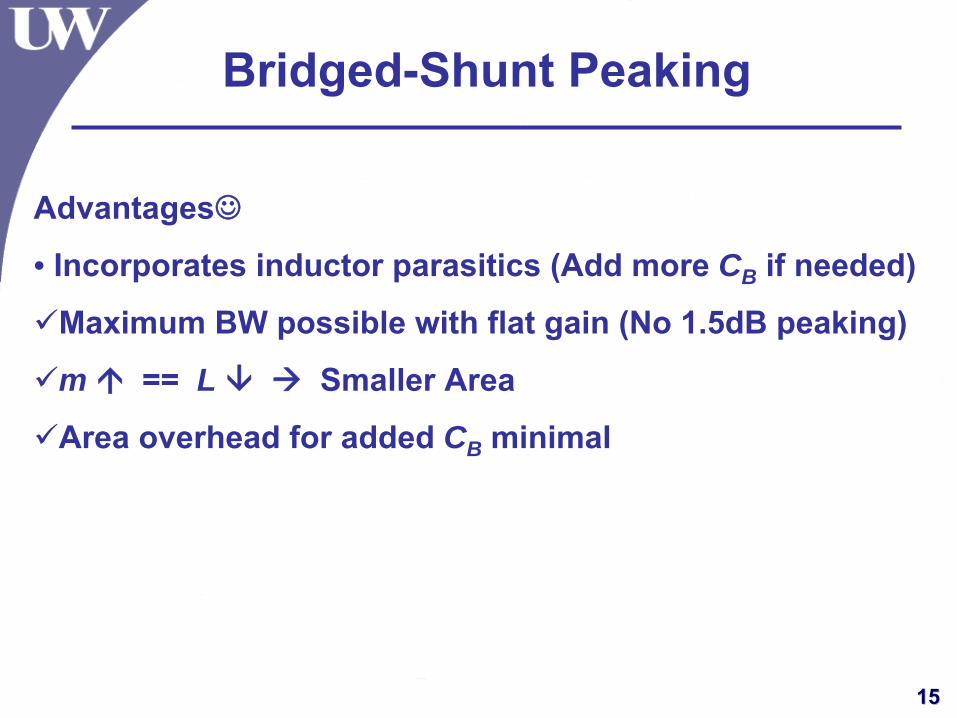
Advantages
• Incorporates inductor parasitics (Add more CB if needed)
Maximum BW possible with flat gain (No 1.5dB peaking)
m == L Smaller Area
Area overhead for added CB minimal
1616
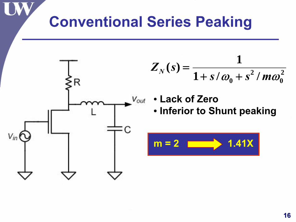
Conventional Series Peaking
20
20 //1
1)(ωω mss
sZN ++=
1.41Xm = 2
• Lack of Zero• Inferior to Shunt peaking
1717
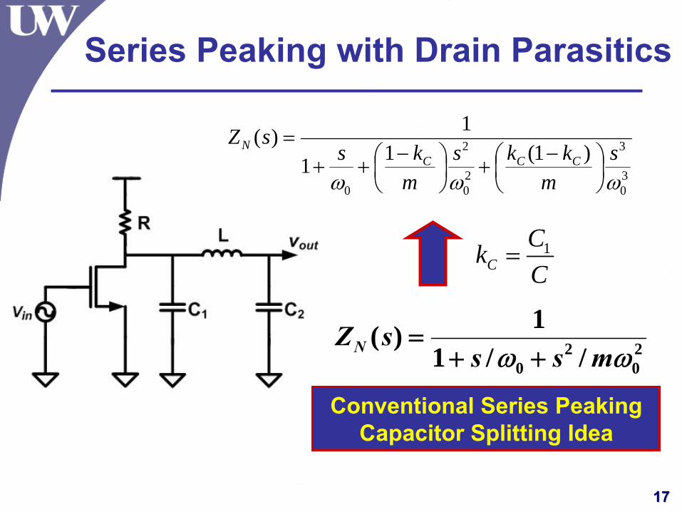
Series Peaking with Drain Parasitics
20
20 //1
1)(ωω mss
sZN ++=
30
3
20
2
0
)1(11
1)(
ωωωs
mkks
mks
sZCCC
N
⎟⎠⎞
⎜⎝⎛ −
+⎟⎠⎞
⎜⎝⎛ −
++=
1C
CkC
=
Conventional Series PeakingCapacitor Splitting Idea
1818
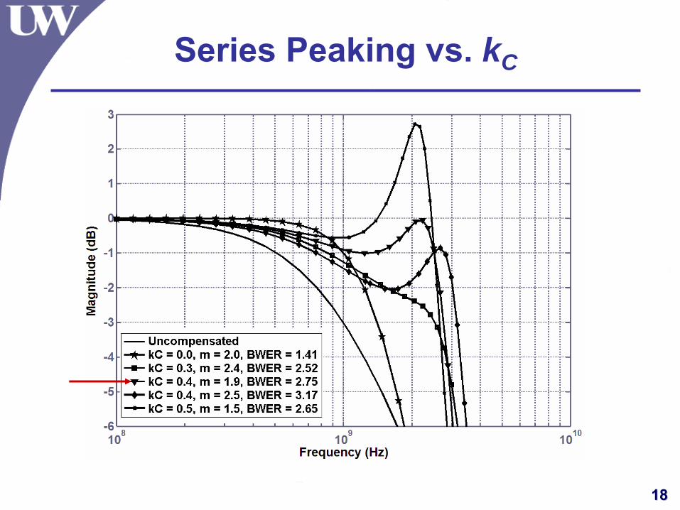
Series Peaking vs. kC
1919
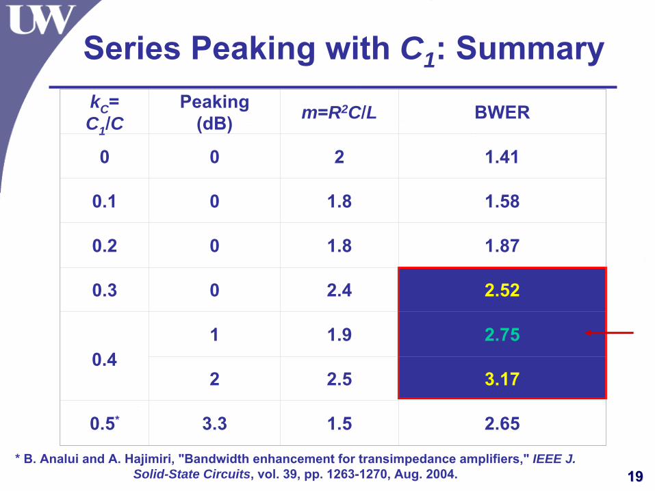
Series Peaking with C1: Summary
0.4
* B. Analui and A. Hajimiri, "Bandwidth enhancement for transimpedance amplifiers," IEEE J. Solid-State Circuits, vol. 39, pp. 1263-1270, Aug. 2004.
kC= C1/C
Peaking (dB) m=R2C/L BWER
0 0 2 1.41
0.1 0 1.8 1.58
0.2 0 1.8 1.87
0.3 0 2.4 2.52
0.4 1 1.9 2.75
2 2.5 3.17
0.5* 3.3 1.5 2.65
2020
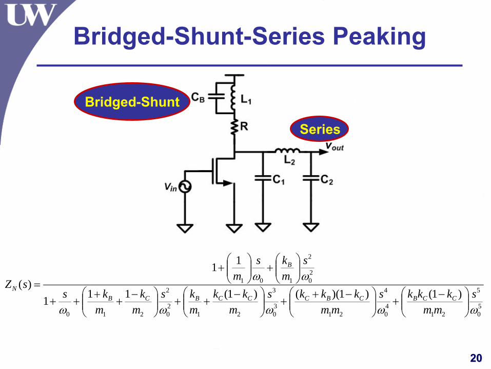
Bridged-Shunt-Series Peaking
50
5
2140
4
2130
3
2120
2
210
20
2
101
)1()1)(()1(111
11)(
ωωωωω
ωωs
mmkkks
mmkkks
mkk
mks
mk
mks
smks
msZ
CCBCBCCCBCB
B
N
⎟⎟⎠
⎞⎜⎜⎝
⎛ −+⎟⎟⎠
⎞⎜⎜⎝
⎛ −++⎟⎟⎠
⎞⎜⎜⎝
⎛ −++⎟⎟⎠
⎞⎜⎜⎝
⎛ −++++
⎟⎟⎠
⎞⎜⎜⎝
⎛+⎟⎟
⎠
⎞⎜⎜⎝
⎛+
=
Bridged-Shunt
Series
2121
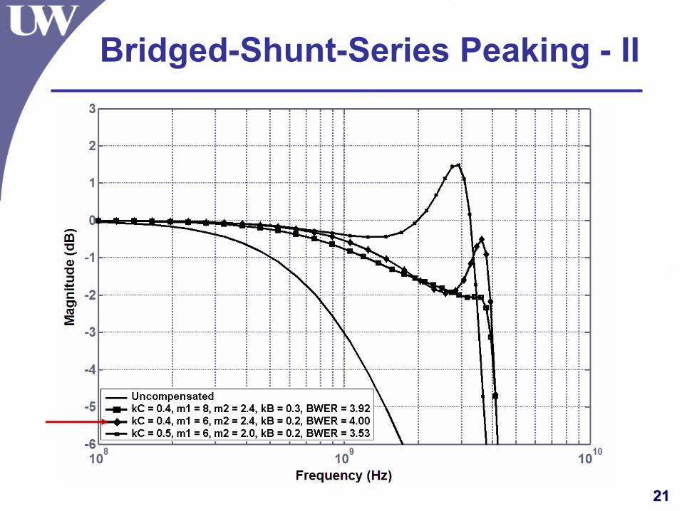
Bridged-Shunt-Series Peaking - II
2222
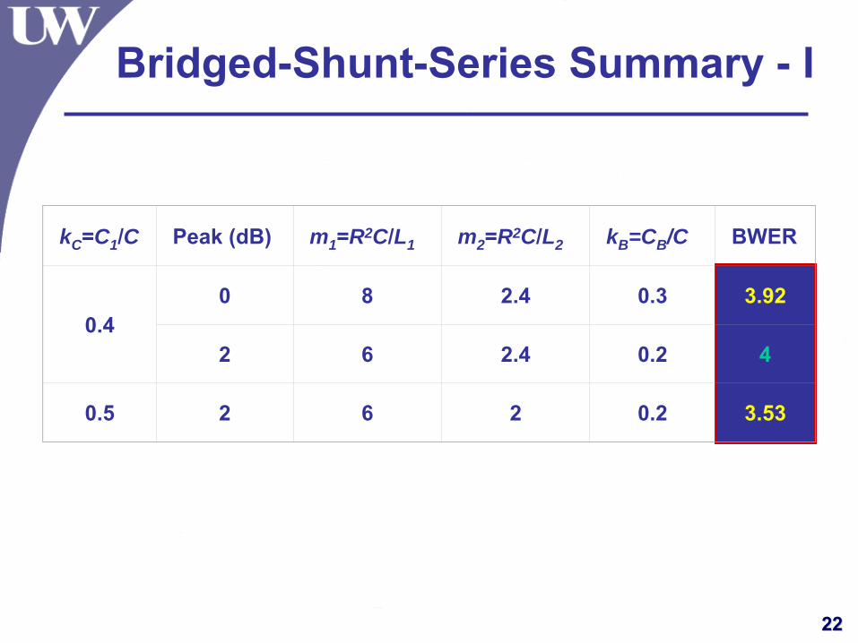
Bridged-Shunt-Series Summary - I
kC=C1/C Peak (dB) m1=R2C/L1 m2=R2C/L2 kB=CB/C BWER
0.40 8 2.4 0.3 3.92
2 6 2.4 0.2 4
0.5 2 6 2 0.2 3.53
2323
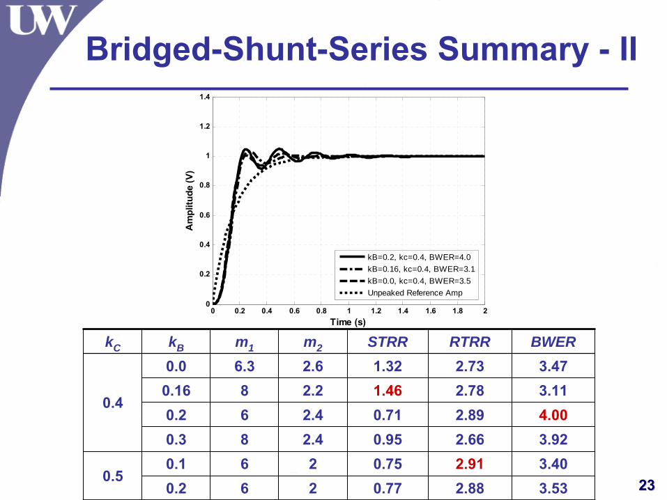
Bridged-Shunt-Series Summary - II
0 0.2 0.4 0.6 0.8 1 1.2 1.4 1.6 1.8 20
0.2
0.4
0.6
0.8
1
1.2
1.4
Time (s)
Am
plitu
de (V
)
kB=0.2, kc=0.4, BWER=4.0kB=0.16, kc=0.4, BWER=3.1kB=0.0, kc=0.4, BWER=3.5Unpeaked Reference Amp
3.532.880.77260.23.402.910.75260.1
0.5
3.922.660.952.480.34.002.890.712.460.23.112.781.462.280.163.472.731.322.66.30.0
0.4
BWERRTRRSTRRm2m1kBkC
2424
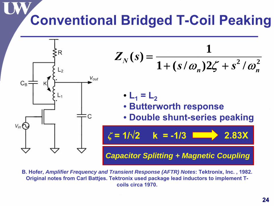
Conventional Bridged T-Coil Peaking
22 /2)/(11)(
nnN sssZ
ωζω ++=
ζ = 1/√2 k = -1/3 2.83X
• L1 = L2• Butterworth response• Double shunt-series peaking
B. Hofer, Amplifier Frequency and Transient Response (AFTR) Notes: Tektronix, Inc. , 1982. Original notes from Carl Battjes. Tektronix used package lead inductors to implement T-
coils circa 1970.
Capacitor Splitting + Magnetic Coupling
2525
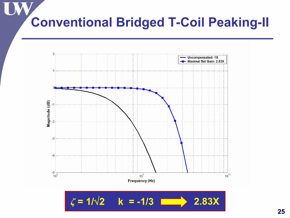
Conventional Bridged T-Coil Peaking-II
ζ = 1/√2 k = -1/3 2.83X
2626
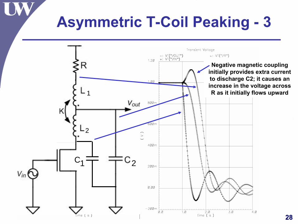
Asymmetric T-Coil Peaking - 1
40
4
21
2
30
3
220
2
21210
0211
)1)(1()1(211
11)(
ωωωω
ω
smm
kkksm
kksmmkk
mk
ms
smm
km
sZmCCCCmCC
m
N
⎟⎟⎠
⎞⎜⎜⎝
⎛ −−+⎟⎟⎠
⎞⎜⎜⎝
⎛ −+⎟⎟⎠
⎞⎜⎜⎝
⎛++++
⎟⎟⎠
⎞⎜⎜⎝
⎛++
=
21/ LLMkm =
1C
CkC
=
2727
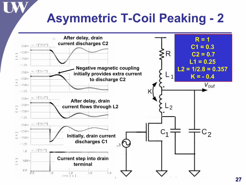
Asymmetric T-Coil Peaking - 2
C1 2
2
1
R = 1 C1 = 0.3 C2 = 0.7
L1 = 0.25 L2 = 1/2.8 = 0.357
K = - 0.4
Current step into drain terminal
Initially, drain current discharges C1
After delay, drain current discharges C2
Negative magnetic coupling initially provides extra current
to discharge C2
After delay, drain current flows through L2
2828
Asymmetric T-Coil Peaking - 3
C1 2
2
1
Negative magnetic coupling initially provides extra current to discharge C2; it causes an increase in the voltage across R as it initially flows upward
2929
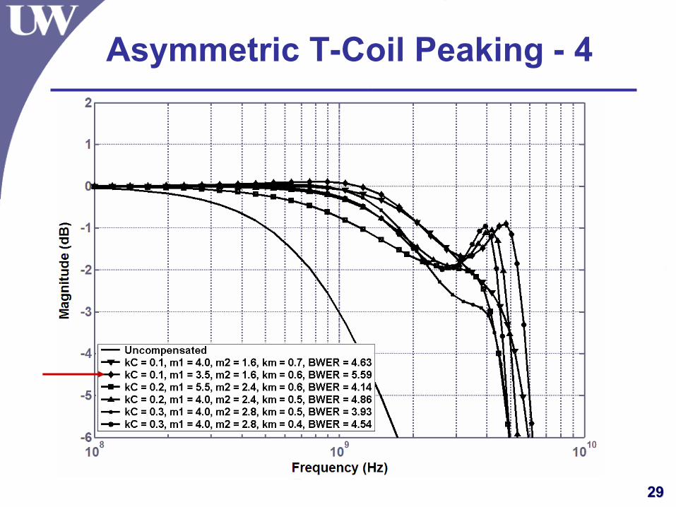
Asymmetric T-Coil Peaking - 4
3030
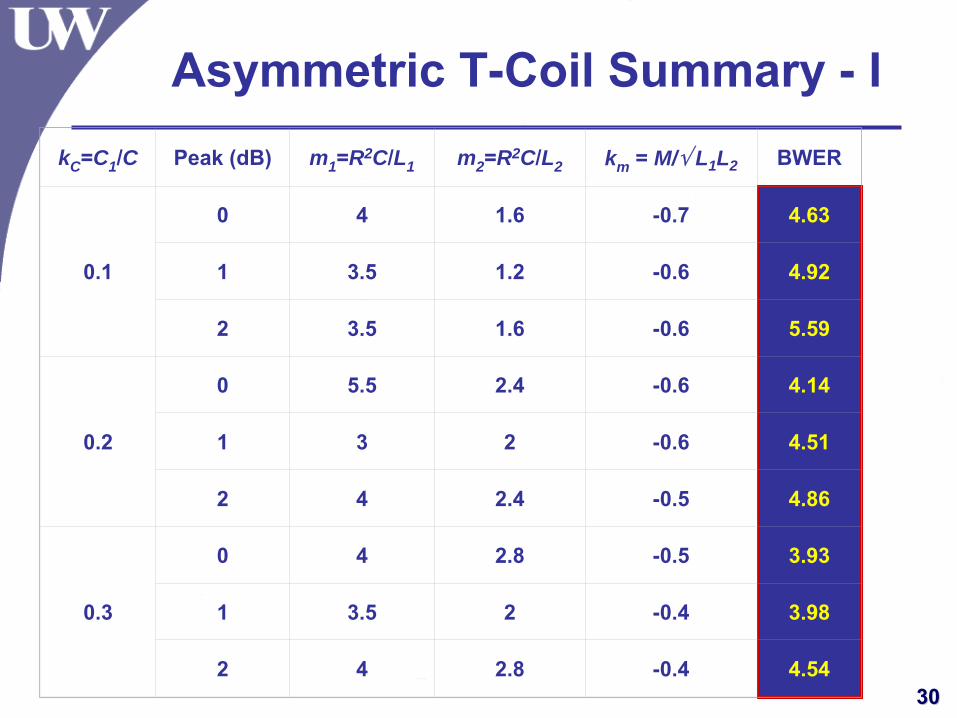
Asymmetric T-Coil Summary - IkC=C1/C Peak (dB) m1=R2C/L1 m2=R2C/L2 km = M/√ L1L2 BWER
0.1
0 4 1.6 -0.7 4.63
1 3.5 1.2 -0.6 4.92
2 3.5 1.6 -0.6 5.59
0.2
0 5.5 2.4 -0.6 4.14
1 3 2 -0.6 4.51
2 4 2.4 -0.5 4.86
0.3
0 4 2.8 -0.5 3.93
1 3.5 2 -0.4 3.98
2 4 2.8 -0.4 4.54
3131
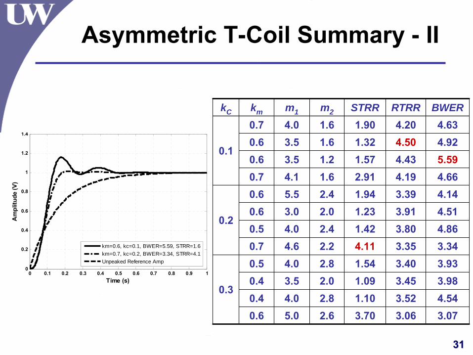
Asymmetric T-Coil Summary - II
0 0.1 0.2 0.3 0.4 0.5 0.6 0.7 0.8 0.9 10
0.2
0.4
0.6
0.8
1
1.2
1.4
Time (s)
Am
plitu
de (V
)
km=0.6, kc=0.1, BWER=5.59, STRR=1.6km=0.7, kc=0.2, BWER=3.34, STRR=4.1Unpeaked Reference Amp
3.073.063.702.65.00.64.543.521.102.84.00.43.983.451.092.03.50.43.933.401.542.84.00.5
0.3
3.343.354.112.24.60.74.863.801.422.44.00.54.513.911.232.03.00.64.143.391.942.45.50.6
0.2
4.664.192.911.64.10.75.594.431.571.23.50.64.924.501.321.63.50.64.634.201.901.64.00.7
0.1
BWERRTRRSTRRm2m1kmkC
3232
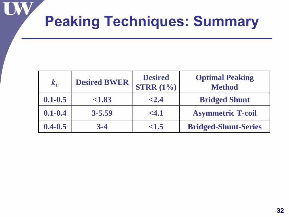
Peaking Techniques: Summary
Bridged-Shunt-Series<1.53-40.4-0.5
Asymmetric T-coil<4.13-5.590.1-0.4
Bridged Shunt<2.4<1.830.1-0.5
Optimal Peaking Method
Desired STRR (1%)Desired BWERkC
3333
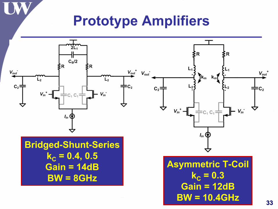
Prototype Amplifiers
Bridged-Shunt-SerieskC = 0.4, 0.5Gain = 14dBBW = 8GHz
Asymmetric T-CoilkC = 0.3
Gain = 12dBBW = 10.4GHz
3434
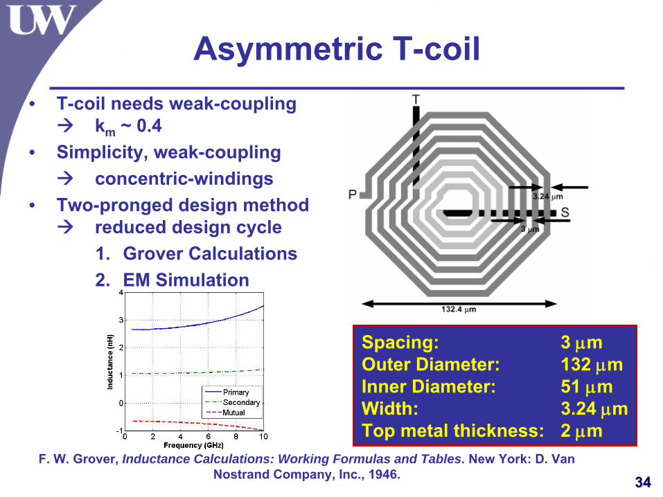
Asymmetric T-coil• T-coil needs weak-coupling
km ~ 0.4• Simplicity, weak-coupling
concentric-windings • Two-pronged design method
reduced design cycle1. Grover Calculations2. EM Simulation
Spacing: 3 μmOuter Diameter: 132 μmInner Diameter: 51 μmWidth: 3.24 μmTop metal thickness: 2 μm
F. W. Grover, Inductance Calculations: Working Formulas and Tables. New York: D. Van Nostrand Company, Inc., 1946.
3535
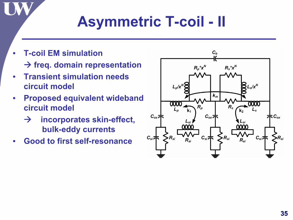
Asymmetric T-coil - II
• T-coil EM simulation freq. domain representation
• Transient simulation needs circuit model
• Proposed equivalent wideband circuit model
incorporates skin-effect, bulk-eddy currents
• Good to first self-resonance
3636
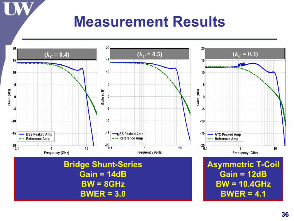
(a) (b) (c)
B
(kC = 0.4) (kC = 0.5) (kC = 0.3)
Measurement Results
Bridge Shunt-SeriesGain = 14dBBW = 8GHzBWER = 3.0
Asymmetric T-CoilGain = 12dB
BW = 10.4GHzBWER = 4.1
3737
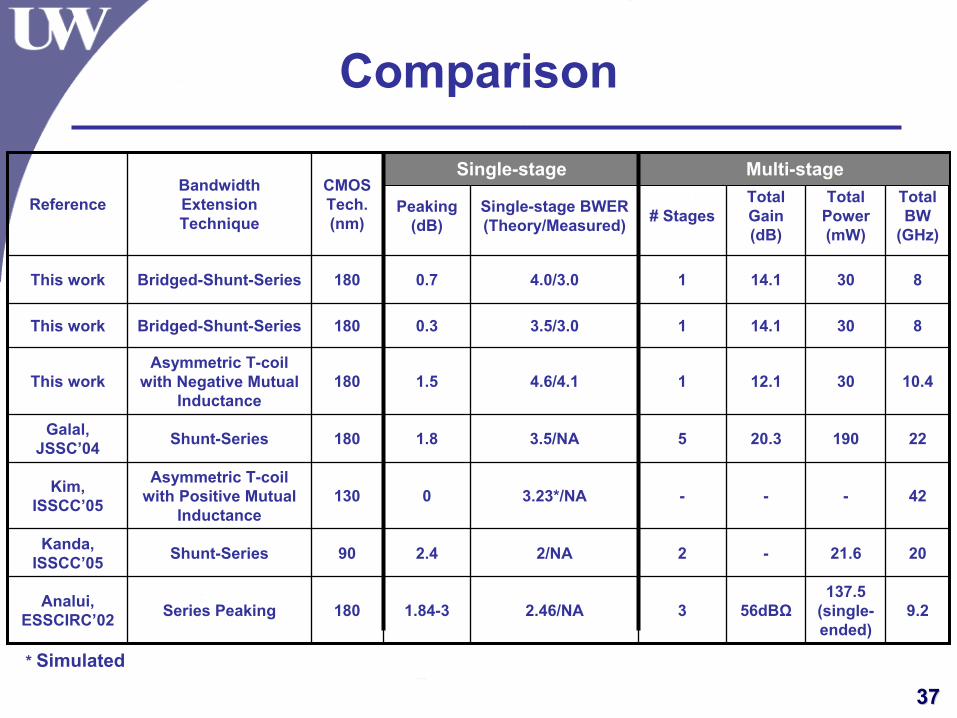
Comparison
137.5 (single-ended)
21.6
-
190
30
30
30
Total Power (mW)
56dBΩ
-
-
20.3
12.1
14.1
14.1
Total Gain (dB)
3
2
-
5
1
1
1
# Stages
2.46/NA
2/NA
3.23*/NA
3.5/NA
4.6/4.1
3.5/3.0
4.0/3.0
Single-stage BWER (Theory/Measured)
80.3180Bridged-Shunt-SeriesThis work
9.21.84-3180Series PeakingAnalui, ESSCIRC’02
90
130
180
180
180
CMOS Tech. (nm)
202.4Shunt-SeriesKanda, ISSCC’05
10.41.5Asymmetric T-coil
with Negative Mutual Inductance
This work
42
22
8
Total BW
(GHz)
0Asymmetric T-coil
with Positive Mutual Inductance
Kim, ISSCC’05
1.8Shunt-SeriesGalal, JSSC’04
0.7Bridged-Shunt-SeriesThis work
Peaking (dB)
Bandwidth Extension Technique
Reference
* Simulated
Single-stage Multi-stage
3838
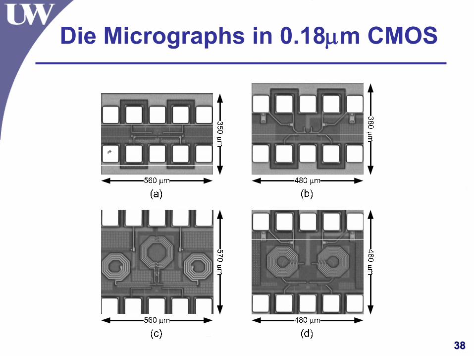
Die Micrographs in 0.18μm CMOS
3939
Conclusions
• Peaking techniques for larger BW extension
• Applicable to different kC constraints
• Trade-off gain flatness for BW
• Amplifiers show large gain (>12dB) with largest BWER (4.1) reported.
• Wide bandwidth, high gain fewer stages power, area savings
4040
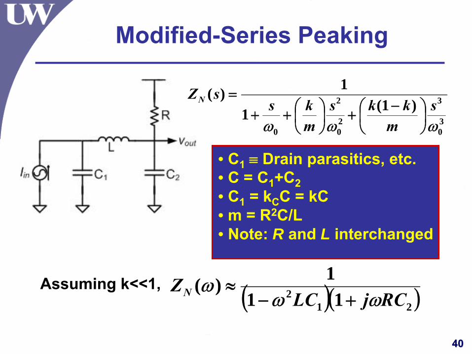
Modified-Series Peaking
• C1 ≡ Drain parasitics, etc. • C = C1+C2• C1 = kCC = kC• m = R2C/L• Note: R and L interchanged
30
3
20
2
0
)1(1
1)(
ωωωs
mkks
mks
sZN⎟⎠⎞
⎜⎝⎛ −+⎟
⎠⎞
⎜⎝⎛++
=
( )( )212 11
1)(RCjLC
ZN ωωω
+−≈Assuming k<<1,
4141
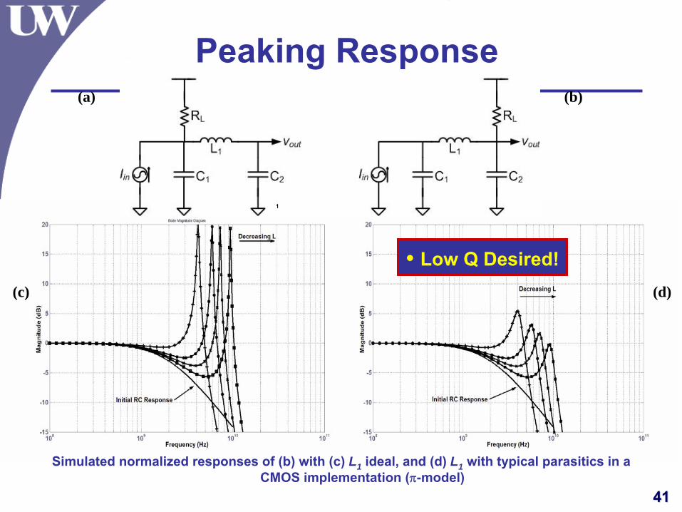
(a) (b)
(c) (d)
1
1
Simulated normalized responses of (b) with (c) L1 ideal, and (d) L1 with typical parasitics in a CMOS implementation (π-model)
Peaking Response
• Low Q Desired!
4242
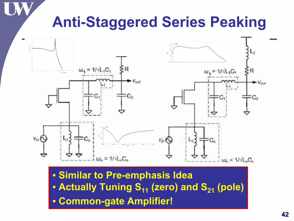
Anti-Staggered Series Peaking
• Similar to Pre-emphasis Idea• Actually Tuning S11 (zero) and S21 (pole)• Common-gate Amplifier!
4343
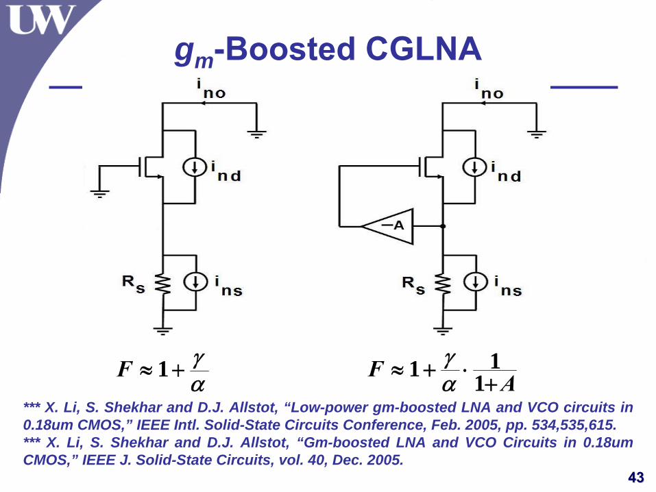
gm-Boosted CGLNA
AF+
⋅+≈ 111 α
γαγ+≈ 1F
*** X. Li, S. Shekhar and D.J. Allstot, “Low-power gm-boosted LNA and VCO circuits in 0.18um CMOS,” IEEE Intl. Solid-State Circuits Conference, Feb. 2005, pp. 534,535,615.*** X. Li, S. Shekhar and D.J. Allstot, “Gm-boosted LNA and VCO Circuits in 0.18um CMOS,” IEEE J. Solid-State Circuits, vol. 40, Dec. 2005.
4444
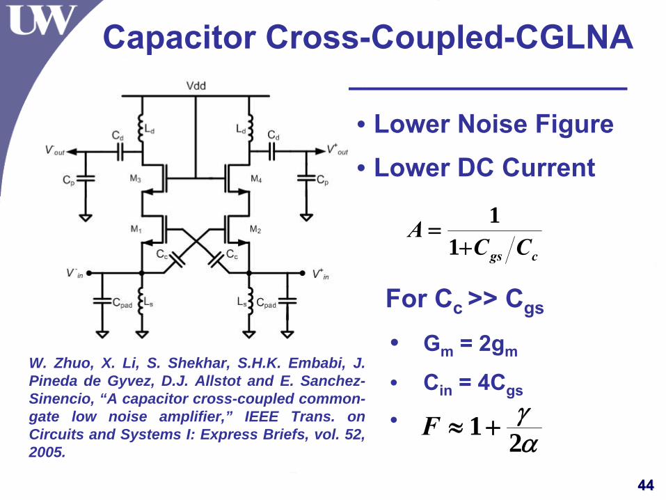
Capacitor Cross-Coupled-CGLNA
• Lower Noise Figure• Lower DC Current
For Cc >> Cgs
• Gm = 2gm
• Cin = 4Cgs
•αγ
21 +≈F
cgs CCA
+=
11
W. Zhuo, X. Li, S. Shekhar, S.H.K. Embabi, J. Pineda de Gyvez, D.J. Allstot and E. Sanchez-Sinencio, “A capacitor cross-coupled common-gate low noise amplifier,” IEEE Trans. on Circuits and Systems I: Express Briefs, vol. 52, 2005.
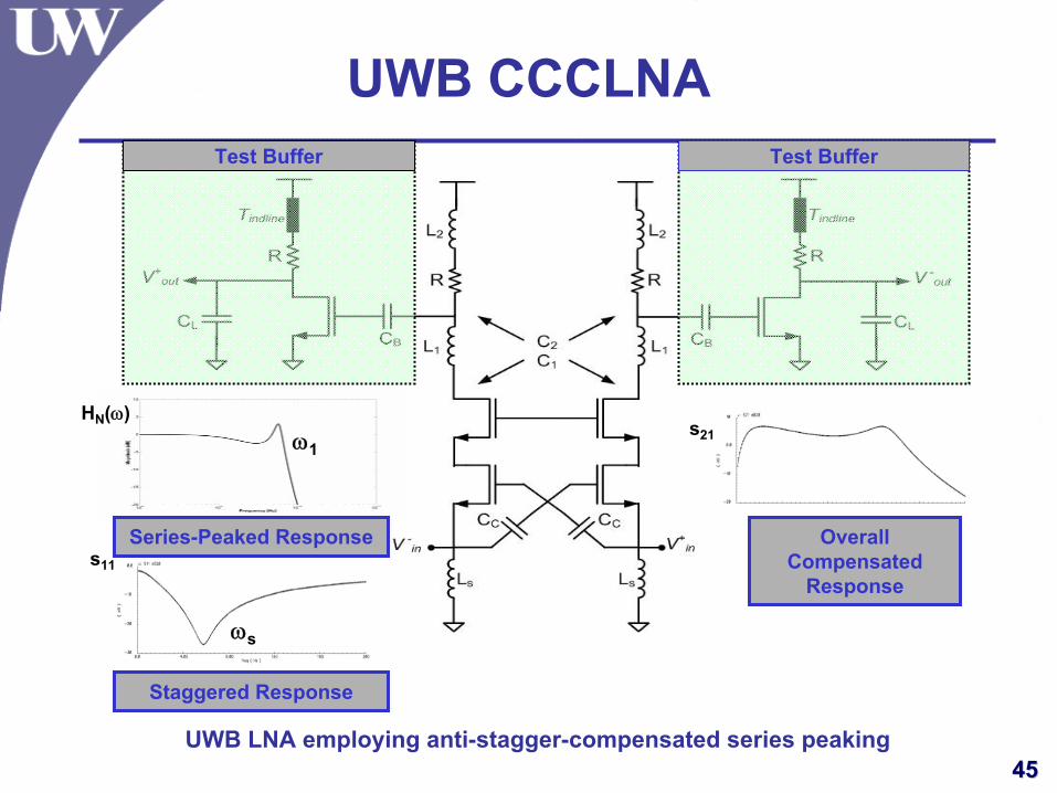
4545UWB LNA employing anti-stagger-compensated series peaking
ω1s21
ωs
s11
HN(ω)
Series-Peaked Response
Staggered Response
Overall Compensated
Response
Test Buffer Test Buffer
UWB CCCLNA
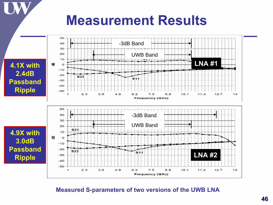
4646Measured S-parameters of two versions of the UWB LNA
UWB Band
-3dB Band
LNA #1
UWB Band
-3dB Band
LNA #2
Measurement Results
4.1X with 2.4dB
PassbandRipple
4.9X with 3.0dB
PassbandRipple
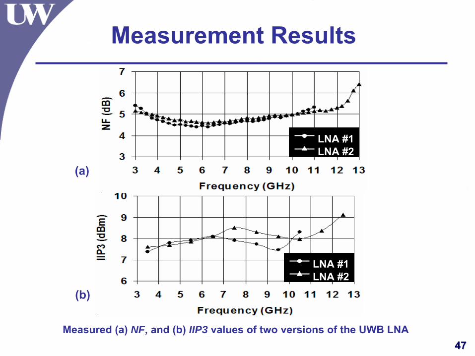
4747Measured (a) NF, and (b) IIP3 values of two versions of the UWB LNA
(a)
(b)
LNA #1LNA #2
LNA #1LNA #2
Measurement Results
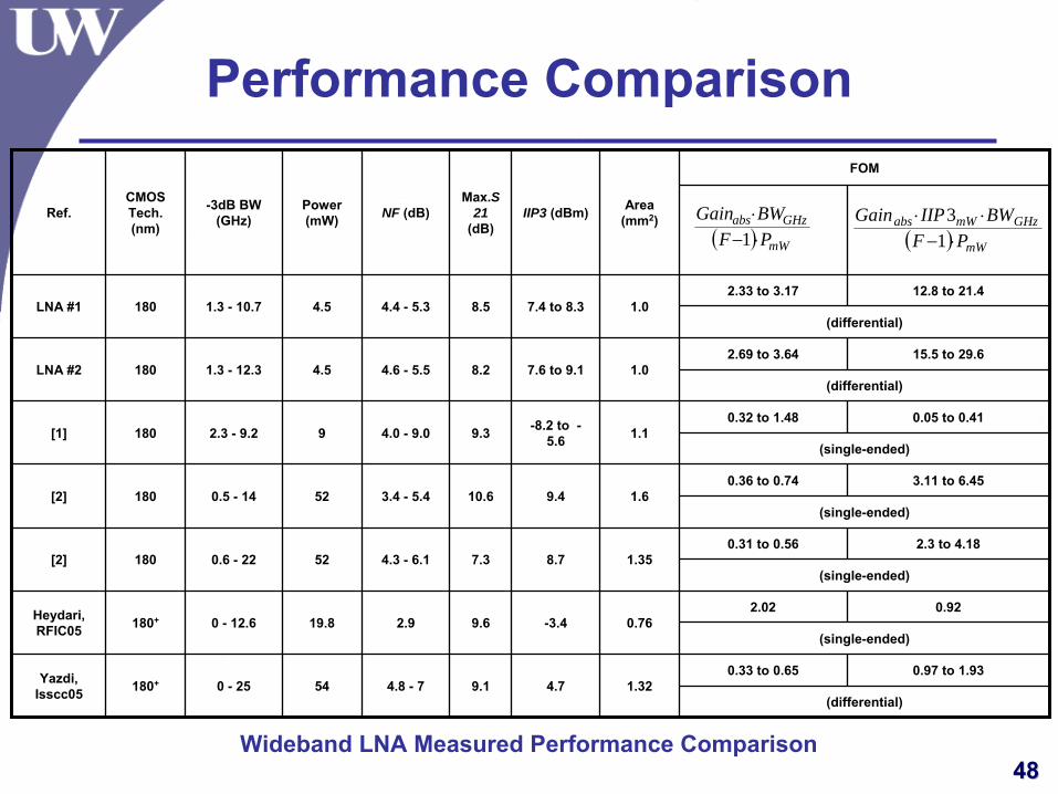
4848
(differential)
(single-ended)
(single-ended)
(single-ended)
(single-ended)
(differential)
(differential)
0.922.020.76-3.49.62.919.80 - 12.6180+Heydari,
RFIC05
2.3 to 4.180.31 to 0.56 1.358.77.34.3 - 6.1520.6 - 22180[2]
15.5 to 29.62.69 to 3.641.07.6 to 9.18.24.6 - 5.54.51.3 - 12.3180LNA #2
0.33 to 0.65
0.36 to 0.74
0.32 to 1.48
2.33 to 3.17
FOM
54
52
9
4.5
Power (mW)
0.97 to 1.931.324.79.14.8 - 70 - 25180+Yazdi,
Isscc05
3.11 to 6.451.69.410.63.4 - 5.40.5 - 14180[2]
0.05 to 0.41 1.1-8.2 to -
5.69.34.0 - 9.02.3 - 9.2180[1]
12.8 to 21.4 1.07.4 to 8.38.54.4 - 5.31.3 - 10.7180LNA #1
Area (mm2)IIP3 (dBm)
Max.S21
(dB)NF (dB)-3dB BW
(GHz)
CMOS Tech. (nm)
Ref.
Wideband LNA Measured Performance Comparison
( ) mW
GHzabsPFBWGain⋅−⋅
1 ( ) mW
GHzmWabsPF
BWIIPGain⋅−
⋅⋅13
Performance Comparison
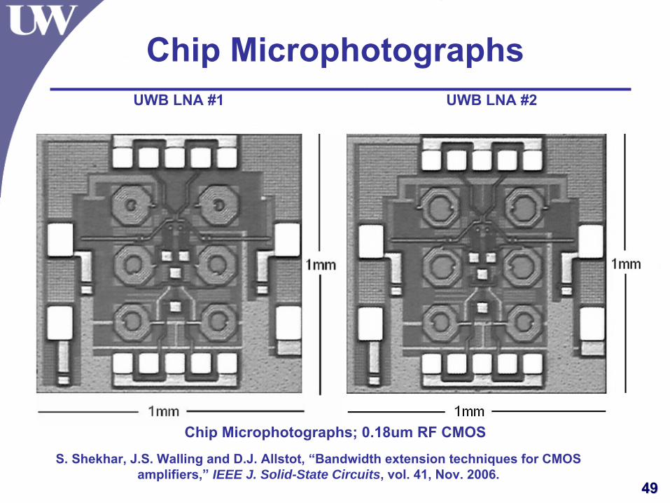
4949
Chip Microphotographs; 0.18um RF CMOS
UWB LNA #1 UWB LNA #2
Chip Microphotographs
S. Shekhar, J.S. Walling and D.J. Allstot, “Bandwidth extension techniques for CMOS amplifiers,” IEEE J. Solid-State Circuits, vol. 41, Nov. 2006.
5050
Conclusions
• Pros Large Bandwidth ExtensionLow PowerSimple Input MatchLow Inductor CountFlat Noise Figure
• Cons Low GainBandwidth Extension Requires Two Stages/Nodes3dB Ripple Too Large for Some ApplicationsSensitive Tuning