Applying Complementary Trap Characterization Technique to...
10
IEEE TRANSACTIONS ON ELECTRON DEVICES, VOL. 57, NO. 11, NOVEMBER 2010 2907 Applying Complementary Trap Characterization Technique to Crystalline γ -Phase-Al 2 O 3 for Improved Understanding of Nonvolatile Memory Operation and Reliability Mohammed B. Zahid, Daniel Ruiz Aguado, R. Degraeve, W. C. Wang, Bogdan Govoreanu, Member, IEEE, María Toledano-Luque, V. V. Afanas’ev, and Jan Van Houdt, Senior Member, IEEE Abstract—The operation and reliability of nonvolatile memory concepts based on charge storage in nitride layers, such as TANOS (TaN/Al 2 O 3 /Si 3 N 4 /SiO 2 /Si), require detailed information on the energy and spatial distribution of the charge defects in both the nitride and the Al 2 O 3 blocking dielectric. This paper focuses on the characterization of Al 2 O 3 . We have successfully applied complementary trap characterization techniques to crystalline γ -phase-Al 2 O 3 in order to obtain a complete picture of the spatial and energetic distribution of the defect density. As a result, two defect types at energy levels 1.8 and 3.5 eV below the conduction band edge are found. Index Terms—Charge trap (CT) memory, crystalline Al 2 O 3 , photodepopulation spectroscopy (PDS), TANOS, trap characteri- zation, trap spectroscopy by charge injection and sensing (TSCIS), two-pulse C –V . I. I NTRODUCTION A GGRESSIVE scaling of Flash memory technology, driven by a continuing demand for higher density and lower costs, opens opportunities for charge trap (CT) Flash memory to extend the lifetime of the floating-gate Flash mem- ory to below 30 nm technology nodes [1]. The tunnel oxide in conventional CT Flash however lacks scalability to below 4–5 nm, which leads to a series of shortcomings, e.g., the program/erase window and/or speed at operating voltages. These make the classical silicon–oxide–nitride–oxide–silicon (SONOS) structure unattractive for standalone Flash mem- ory. In order to address such issues, high-k materials have Manuscript received March 22, 2010; revised June 21, 2010; accepted August 5, 2010. Date of publication September 30, 2010; date of current version November 5, 2010. This work was supported in part by the EC through Project Gossamer “Giga-scale oriented solid-state Flash memory for Europe” and in part by imec’s Industrial Affiliation Program on Advanced Flash Memory. The review of this paper was arranged by Editor D. Esseni. M. B. Zahid, R. Degraeve, B. Govoreanu, and J. Van Houdt are with imec, 3001 Leuven, Belgium (e-mail: [email protected]). D. R. Aguado is with imec, 3001 Leuven, Belgium, and also with the ESAT Department, Katholieke Universiteit Leuven, 3001 Leuven, Belgium. W. C. Wang and V. V. Afanas’ev are with the Department of Physics and Astronomy and the Institute for Nanoscale Physic and Chemistry (INPAC), University of Leuven, 3001 Leuven, Belgium. M. Toledano-Luque is with imec, 3001 Leuven, Belgium, on leave from the Departamento Física Aplicada III, Universidad Complutense de Madrid, Ciudad Universitaria, 28040 Madrid, Spain. Color versions of one or more of the figures in this paper are available online at http://ieeexplore.ieee.org. Digital Object Identifier 10.1109/TED.2010.2071071 been proposed to replace the blocking dielectric [2], even- tually in combination with metal gate, leading to TANOS (TaN (TiN)/Al 2 O 3 /Si 3 N 4 /SiO 2 /Si) CT memory. The high-k/ metal gate solution also received attention in floating-gate tech- nology, where high-k interpolydielectrics (IPD) can eventually compensate for the cell coupling-capacitance loss induced by architectural modifications imminent below 45-nm nodes. In contrast to most high-k materials, such as HfO 2 [3], [4], ZrO 2 [5]–[8], and TiO 2 [9], for which higher dielectric constant usually comes at the expense of narrower band gap, typically in the range of 5–6 eV [10], [11] and, consequently, lower barrier heights for electrons and holes, which determine leakage current, Al 2 O 3 has, apart from stable chemical and thermal properties, material characteristics that rank it high in view of application to NVM technologies, e.g., a band gap similar to SiO 2 , high barrier offset, and a dielectric constant more than double that of SiO 2 . Consequently, Al 2 O 3 [12], [13] has received considerable attention in the development of nonvolatile memories (NVMs), mainly as replacement for blocking dielectric in TANOS or for IPD in floating-gate cells, where state-of-the-art oxide–nitride–oxide (ONO) stacks lack scalability to below 10 nm [14]. Al 2 O 3 is also interesting in NVM technologies because of the persistence of its insulating properties (e.g., large band gap) after crystallization, which makes it compatible with conventional processes that involve high temperatures above 1000 ◦ C [15]. Unfortunately, Al 2 O 3 has significantly more electron traps, compared with SiO 2 [16]– [18], which act detrimentally for NVM reliability. As shown by Mehta et al. [33] using photoinjection–photodepopulation, defects are present in the energy range 1.8–3.6 eV below E c (Al 2 O 3 ). More recently, Kim et al. [34] showed, using photoconductivity, the existence of two dominant trap levels, located at around 2 and 4 eV below E c (Al 2 O 3 ). In this context, it is important to investigate and understand the as-processed and the stress-induced defects in Al 2 O 3 . The optimization of Al 2 O 3 and the necessity of overcoming the reliability concerns [19], [20] require a thorough understanding of the distribution of electrical defects. The aim of this work is to apply complementary trap characterization techniques to crystalline γ -phase-Al 2 O 3 in order to obtain a complete picture of the spatial and energetic distribution of the defect density. We only aim at characterizing 0018-9383/$26.00 © 2010 IEEE
Transcript of Applying Complementary Trap Characterization Technique to...
IEEE TRANSACTIONS ON ELECTRON DEVICES, VOL. 57, NO. 11, NOVEMBER 2010 2907
Applying Complementary Trap CharacterizationTechnique to Crystalline γ-Phase-Al2O3 for
Improved Understanding of Nonvolatile MemoryOperation and Reliability
Mohammed B. Zahid, Daniel Ruiz Aguado, R. Degraeve, W. C. Wang, Bogdan Govoreanu, Member, IEEE,María Toledano-Luque, V. V. Afanas’ev, and Jan Van Houdt, Senior Member, IEEE
Abstract—The operation and reliability of nonvolatile memoryconcepts based on charge storage in nitride layers, such as TANOS(TaN/Al2O3/Si3N4/SiO2/Si), require detailed information onthe energy and spatial distribution of the charge defects in boththe nitride and the Al2O3 blocking dielectric. This paper focuseson the characterization of Al2O3. We have successfully appliedcomplementary trap characterization techniques to crystallineγ-phase-Al2O3 in order to obtain a complete picture of the spatialand energetic distribution of the defect density. As a result, twodefect types at energy levels 1.8 and 3.5 eV below the conductionband edge are found.
Index Terms—Charge trap (CT) memory, crystalline Al2O3,photodepopulation spectroscopy (PDS), TANOS, trap characteri-zation, trap spectroscopy by charge injection and sensing (TSCIS),two-pulse C–V .
I. INTRODUCTION
AGGRESSIVE scaling of Flash memory technology,driven by a continuing demand for higher density and
lower costs, opens opportunities for charge trap (CT) Flashmemory to extend the lifetime of the floating-gate Flash mem-ory to below 30 nm technology nodes [1]. The tunnel oxidein conventional CT Flash however lacks scalability to below4–5 nm, which leads to a series of shortcomings, e.g., theprogram/erase window and/or speed at operating voltages.These make the classical silicon–oxide–nitride–oxide–silicon(SONOS) structure unattractive for standalone Flash mem-ory. In order to address such issues, high-k materials have
Manuscript received March 22, 2010; revised June 21, 2010; acceptedAugust 5, 2010. Date of publication September 30, 2010; date of current versionNovember 5, 2010. This work was supported in part by the EC through ProjectGossamer “Giga-scale oriented solid-state Flash memory for Europe” and inpart by imec’s Industrial Affiliation Program on Advanced Flash Memory. Thereview of this paper was arranged by Editor D. Esseni.
M. B. Zahid, R. Degraeve, B. Govoreanu, and J. Van Houdt are with imec,3001 Leuven, Belgium (e-mail: [email protected]).
D. R. Aguado is with imec, 3001 Leuven, Belgium, and also with the ESATDepartment, Katholieke Universiteit Leuven, 3001 Leuven, Belgium.
W. C. Wang and V. V. Afanas’ev are with the Department of Physics andAstronomy and the Institute for Nanoscale Physic and Chemistry (INPAC),University of Leuven, 3001 Leuven, Belgium.
M. Toledano-Luque is with imec, 3001 Leuven, Belgium, on leave fromthe Departamento Física Aplicada III, Universidad Complutense de Madrid,Ciudad Universitaria, 28040 Madrid, Spain.
Color versions of one or more of the figures in this paper are available onlineat http://ieeexplore.ieee.org.
Digital Object Identifier 10.1109/TED.2010.2071071
been proposed to replace the blocking dielectric [2], even-tually in combination with metal gate, leading to TANOS(TaN (TiN)/Al2O3/Si3N4/SiO2/Si) CT memory. The high-k/metal gate solution also received attention in floating-gate tech-nology, where high-k interpolydielectrics (IPD) can eventuallycompensate for the cell coupling-capacitance loss induced byarchitectural modifications imminent below 45-nm nodes.
In contrast to most high-k materials, such as HfO2 [3],[4], ZrO2 [5]–[8], and TiO2 [9], for which higher dielectricconstant usually comes at the expense of narrower band gap,typically in the range of 5–6 eV [10], [11] and, consequently,lower barrier heights for electrons and holes, which determineleakage current, Al2O3 has, apart from stable chemical andthermal properties, material characteristics that rank it high inview of application to NVM technologies, e.g., a band gapsimilar to SiO2, high barrier offset, and a dielectric constantmore than double that of SiO2. Consequently, Al2O3 [12],[13] has received considerable attention in the developmentof nonvolatile memories (NVMs), mainly as replacement forblocking dielectric in TANOS or for IPD in floating-gate cells,where state-of-the-art oxide–nitride–oxide (ONO) stacks lackscalability to below 10 nm [14]. Al2O3 is also interesting inNVM technologies because of the persistence of its insulatingproperties (e.g., large band gap) after crystallization, whichmakes it compatible with conventional processes that involvehigh temperatures above 1000 ◦C [15]. Unfortunately, Al2O3
has significantly more electron traps, compared with SiO2 [16]–[18], which act detrimentally for NVM reliability. As shownby Mehta et al. [33] using photoinjection–photodepopulation,defects are present in the energy range 1.8–3.6 eV belowEc (Al2O3). More recently, Kim et al. [34] showed, usingphotoconductivity, the existence of two dominant trap levels,located at around 2 and 4 eV below Ec (Al2O3). In this context,it is important to investigate and understand the as-processedand the stress-induced defects in Al2O3. The optimization ofAl2O3 and the necessity of overcoming the reliability concerns[19], [20] require a thorough understanding of the distributionof electrical defects.
The aim of this work is to apply complementary trapcharacterization techniques to crystalline γ-phase-Al2O3 inorder to obtain a complete picture of the spatial and energeticdistribution of the defect density. We only aim at characterizing
0018-9383/$26.00 © 2010 IEEE
2908 IEEE TRANSACTIONS ON ELECTRON DEVICES, VOL. 57, NO. 11, NOVEMBER 2010
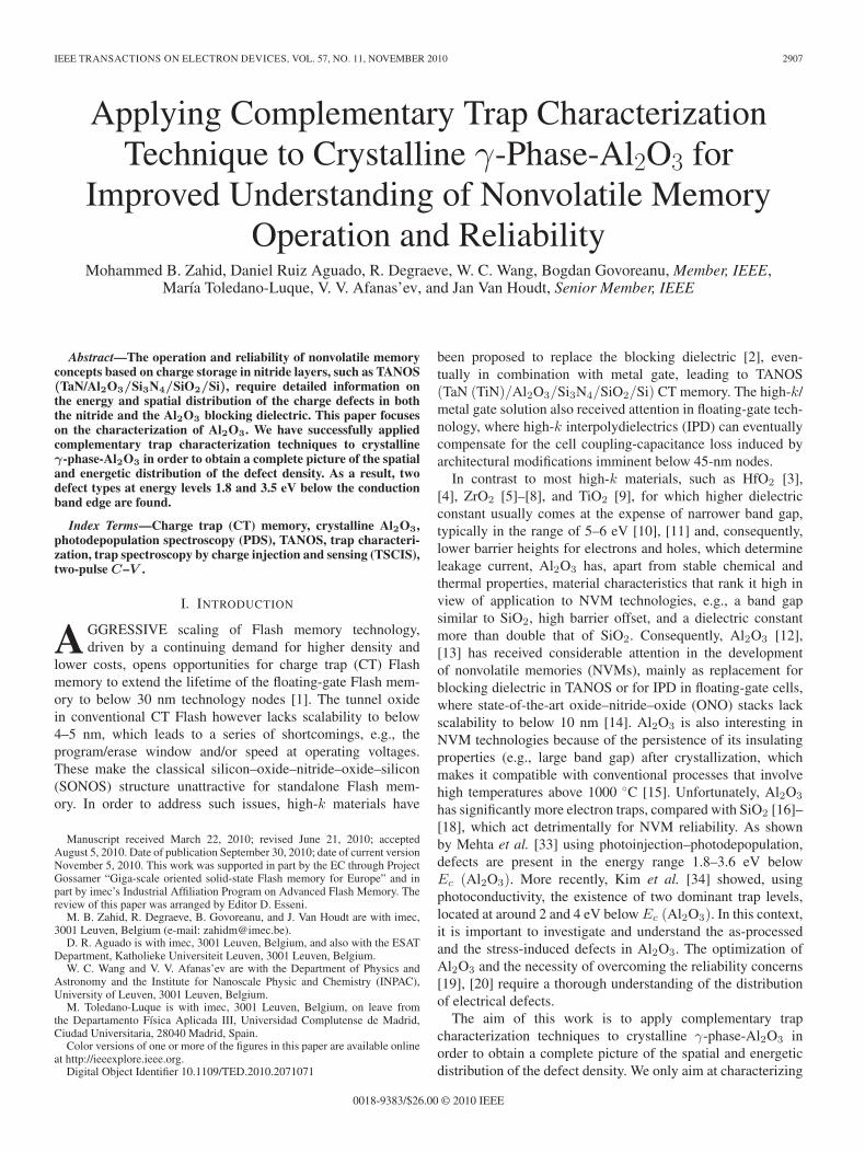
Fig. 1. Schematic drawing of the samples used in this work. (a) MOS capacitor with junction for SS-TSCIS. (b) MOS capacitor with junction for GS-TSCIS.(c) MOS capacitor without junction for PDS. (d) MOS capacitor without junction for 2-PCV. In most cases, a two-layer dielectric stack is used consisting of SiO2
and Al2O3. In some specific cases (see also Table I), a TANOS stack is used.
the bulk properties of the deposited layers on relatively largeareas. For integration into deeply scaled devices, additionalprocessing issues can still modify the defect profiles or inducelocalize damage. This paper is organized as follows: InSection II, the advantages and drawbacks of each characteri-zation technique are described, along with the sample require-ments for each considered techniques. In Section III, we discussthe resulting trap distributions on γ-phase-Al2O3 subjected todifferent thermal treatments, using the techniques described inSection II, and finally, Section IV summarizes the main results.
II. DEVICE AND TECHNIQUE DESCRIPTIONS
A. Devices
The test structures used in this work are MOS capacitors(50 × 50 μm2) with/without junction, as schematized in Fig. 1and listed in Table I, where a dual-layer SiO2/Al2O3 stackor a full TANOS stack are used. The thickness of the tunneloxide of the TANOS stack has been adjusted to provide optimalconditions for controlled charging of the defects in the stack,as it will be explained in Section II. The study of the TANOSstructure has been introduced here to account for the structuralmodifications of the Al2O3 layer, which is eventually inducedby the nitride charge-trapping film.
The gate stack is deposited on p- or n-type Si substrate andhas been manufactured using in situ steam-generated (ISSG)oxidation to grow the bottom SiO2 layer. The Al2O3 filmwas deposited by atomic layer deposition (ALD) at 300 ◦C,in a Polygon 8300 chamber, using trimethly aluminate,Al(CH3)3-TMA, and H2O as precursor. A postdeposition an-neal (PDA) was carried out immediately after Al2O3 depositionand the Al2O3 thickness contraction after annealing was ac-counted for to achieve a target thickness of 10 nm, irrespectiveof the annealing temperature [21].
All samples received a postannealing treatment, as indicatedin Table I. After the gate stack formation, TaN or TiN wasdeposited using postvapor deposition or 15-nm Au electrodesof 0.5-mm2 area were evaporated in high vacuum from aresistively heated boat on cold substrate.
B. Techniques
This section describes the complementary and independent(from each other) trap characterization techniques applied to
our test structures with crystalline γ-phase-Al2O3 in order toobtain a complete picture of the spatial and energetic distrib-ution of the defect density. Note that charge pumping is notincluded in the list below, since it is mainly an interface char-acterization technique, while in this paper we aim at character-izing the bulk defects in the Al2O3. As shown in [32] chargepumping can scan up to ∼1.2 nm and therefore it cannot giveadditional information in the test structures used in this paper.
1) TSCIS: Trap spectroscopy by charge injection and sens-ing (TSCIS) has been proposed as a powerful method forcharacterizing defect bands in dielectric materials [18], [22].This technique relies on a controlled charging of the Al2O3
traps by electrons injected from either the substrate (substrate-side TSCIS, SS-TSCIS) or the gate electrode (gate-side TSCIS,GS-TSCIS) with the charging voltage Vcharge and the chargingtime tcharge as measurement parameters.
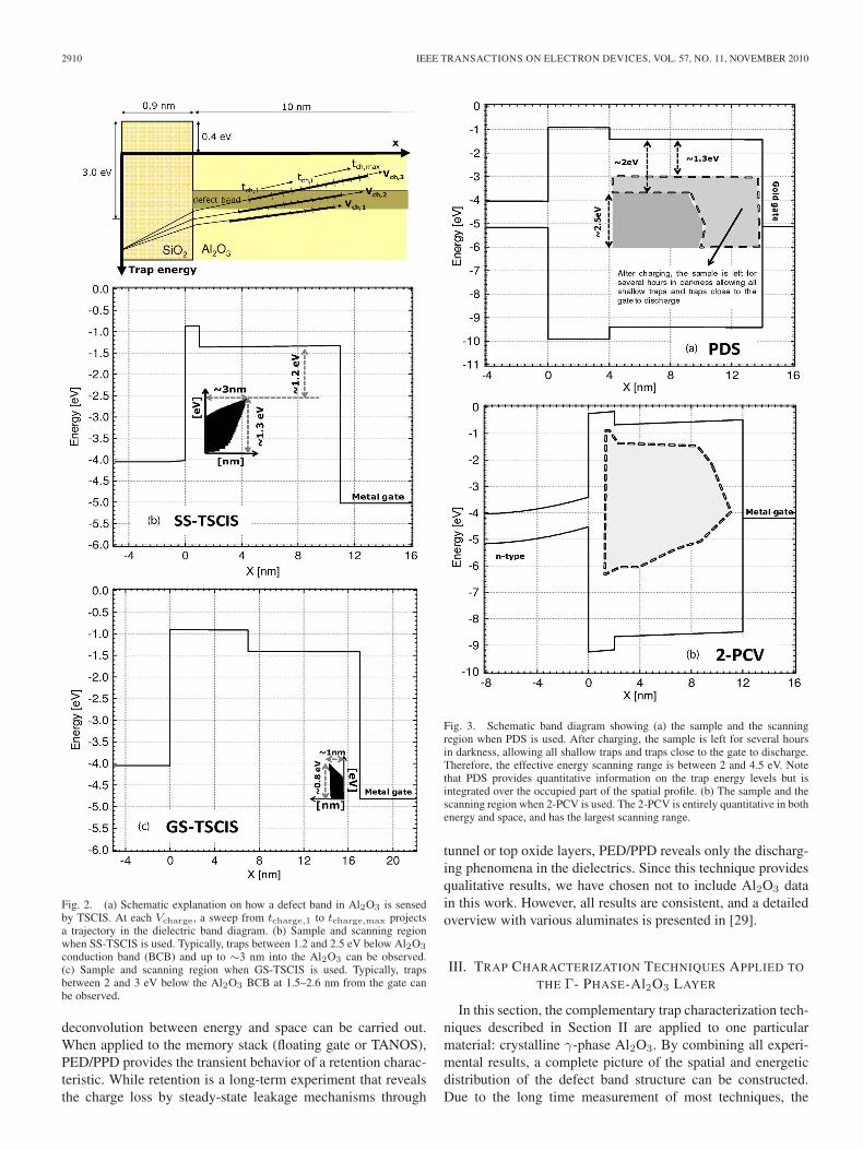
1) SS-TSCIS uses electron injection from the inversionlayer in the substrate at positive Vcharge through a1-nm SiO2 interface layer separating the substrate fromthe Al2O3 [Fig. 2(b)]. By increasing tcharge at eachVcharge, a trajectory in the dielectric band diagram isdefined by the first subband energy level in the inversionlayer at the corresponding tunnel distance [Fig. 2(a)].At low Vcharge, the trajectory encompasses only deeptraps close to the interface, and with increasing Vcharge,the trajectory moves closer to the conduction band edgeand further away from the interface, allowing shallowstates to be occupied by injected electrons [Fig. 2(a)].Since tcharge is mainly a measure of the scanning distancefrom the substrate interface, thick SiO2 requires longertcharge for electrons to tunnel to traps situated in theAl2O3 dielectric layer. A SiO2 thinner than 1 nm would,in principle, reduce the charging time even more, but itmight however not be deposited reliably. The low k valueof the interface layer has an advantage in that it creates acantilever effect similar to that of the VARIOT engineeredbarrier [23] when applying a gate bias Vcharge.
Consequently, eventual traps situated in a relativelywide region of the Al2O3 band gap may line up inenergy with the injection level of the electrons in theinversion layer. These traps may therefore be charged andsubsequently electrically probed by SS-TSCIS. Typically,traps between 1.2 and 2.5 eV below Al2O3 conductionband (BCB) and up to ∼3 nm into the Al2O3 can be
ZAHID et al.: APPLYING TRAP CHARACTERIZATION TO CRYSTALLINE FOR NVM OPERATION AND RELIABILITY 2909
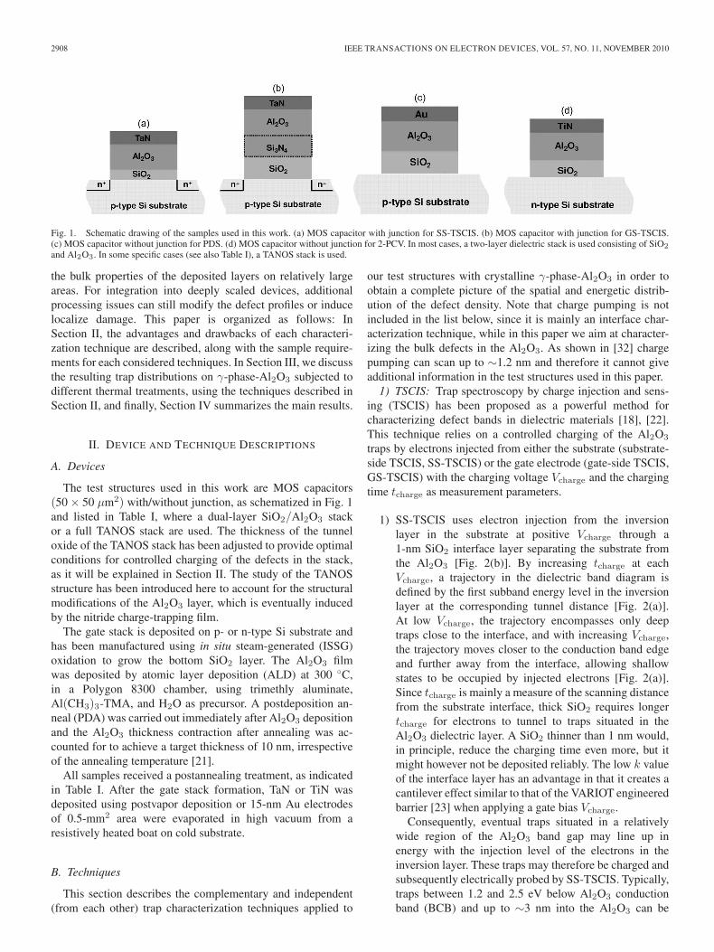
TABLE ISUMMARY OF THE SAMPLES USED IN THIS WORK. THE TABLE DESCRIBES THE STACKS REQUIRED FOR EACH MEASUREMENT TECHNIQUE
(SS/GS-TSCIS: SUBSTRATE-SIDE/GATE-SIDE TRAP SPECTROSCOPY BY CHARGE INJECTION AND SENSING, PDS: PHOTO DEPOPULATION
SPECTROSCOPY, AND 2-PCV: TWO-PULSE CV), INCLUDING THE THICKNESS OF THE SiO2, PROCESS CONDITION, AND GATE MATERIAL
observed [24]. In Fig. 2(b), the possible scanning regionis indicated by the shaded area.
2) Similar to SS-TSCIS, GS-TSCIS uses electron injectionfrom the metal gate at negative Vcharge and is thereforeparticularly useful for characterizing defects near theAl2O3/metal gate interface [22]. Note that, in this case,the SiO2 interface layer should be thick enough to avoidparasitic hole injection from or electron discharging tothe substrate when applying a negative Vcharge. The insu-lating capability of the interface layer limits the energyscanning range. The thicker the SiO2, the higher therange; therefore, we use samples with 7-nm SiO2
[Fig. 2(c)]. Since a Si3N4 layer can be inserted betweenthe interface SiO2 and the Al2O3, GS-TSCIS can also becarried out on a full TANOS stack, even with layer thick-nesses corresponding to an operational memory stack(4/6/10 nm SiO2/Si3N4/Al2O3). The possible scanningregion of GS-TSCIS is indicated by the shaded area inFig. 2(c). Note that, for GS-TSCIS, the scanned energyrange is deeper w.r.t. the Al2O3 BCB because of thehigher band offset of the metal gate, compared with Si.Typically, traps between 2 and 3 eV below the Al2O3
BCB at 1.5–2.6 nm from the gate can be observed.
2) PDS: Photodepopulation spectroscopy (PDS) relies oncontrolled discharging of trapped electrons by photoexcitationwith the photon energy as measurement variable [25], [26]. Dueto the nature of the experiment, the gate of the device mustbe transparent to the incident photon flux, and we have used a15-nm Au gate. At high positive voltage, charging of the Al2O3
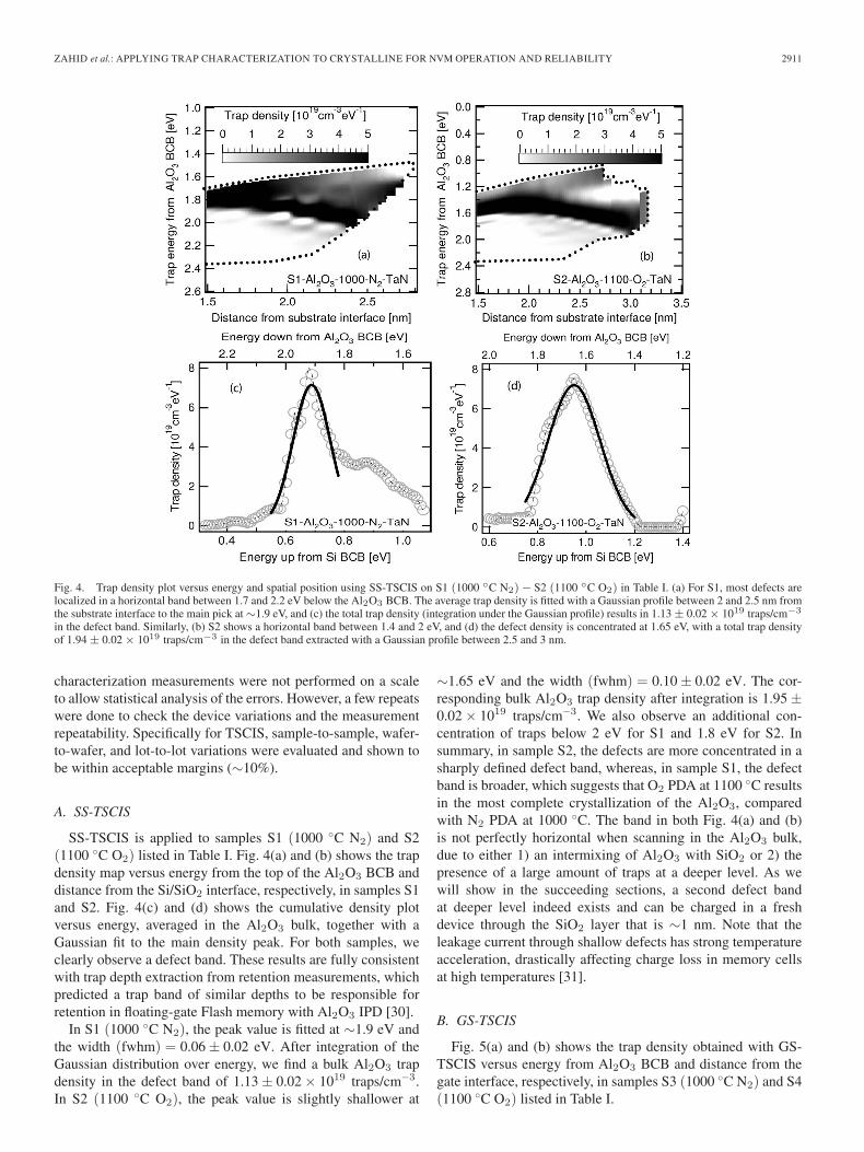
is achieved by electron tunneling through a 4-nm SiO2 tunnel-ing layer. After charging, the sample is left for several hours indarkness, allowing all shallow traps and traps close to the gateto discharge. Therefore, although the photon energy range forexcitation starts from 1.3 eV, electrons trapped at this energylevel are not measured, and the effective energy scanning rangeis narrower, between 2 and 4.5 eV, as indicated in Fig. 3(a)by the shaded area. Note that PDS provides quantitative in-formation on the trap energy levels but is integrated over theoccupied part of the spatial profile. The major advantage of thismethod consists of direct association of the trap photoionization
energy to the energy of the exciting photons. Therefore, nooversimplifying assumptions are invoked, allowing the use ofthe PDS trap distribution as an energy reference for other trapcharacterization techniques.
3) 2-PCV: Like PDS, two-pulse C–V (2-PCV) also relieson the controlled discharging of trapped charge, but the dis-charging is induced by a gate bias allowing electrons to tunnelout of the dielectric as a function of time and applied voltage[27], [28]. Consequently, information on the energy and thespatial distribution of the traps can be extracted. The sample ischarged through a SiO2 tunnel oxide, and then, the dischargeis monitored as the flatband (VFB) variation under differentconditions. Because of the higher time resolution (∼ms range),2-nm SiO2 provides the optimal balance between minimizedmeasurement time and maximum extracted data. The 2-PCVtechnique allows extracting entirely quantitative information onthe traps in both energy and space, and has the largest scanningrange, as indicated by the shaded area in Fig. 3(b).
The difference with the previous techniques is that the spatialand energetic defect profile is not calculated directly fromthe measured values but is reconstructed from a set of trapparameters that allows fitting the entire measured data set. Thephysical model is based on first-order detrapping kinetics formonitoring the variation of the charge trapped in the Al2O3
stack with time while taking into account possible retrappingdue to application of bias during discharging [28]. We haveemployed 2-PCV to confirm the profile of the traps in bothenergy and space detected by SS-TSCIS or PDS. Note that2-PCV requires an n-substrate to avoid parasitic hole injectionduring the application of negative gate bias for discharging.
4) PPD/PED Technique: In the Post-Program and Post-Erase Discharging (PPD/PED) technique, one measures withhigh time resolution the evolution of the flatband (VFB) orthreshold (VTH) voltage immediately after applying a positive(VPROG) or negative (VERASE) voltage pulse. In fact, PPD/PED is a short integrated version of TSCIS with three additionaladvantages: 1) It does not need dedicated structures with a thinSiO2 interface layer and can be used on any samples. 2) It issignificantly less time consuming. 3) It even allows scanningelectrons trap below the Si-conduction band. The disadvantageis that all extracted information remains qualitative, and no
2910 IEEE TRANSACTIONS ON ELECTRON DEVICES, VOL. 57, NO. 11, NOVEMBER 2010
Fig. 2. (a) Schematic explanation on how a defect band in Al2O3 is sensedby TSCIS. At each Vcharge, a sweep from tcharge,1 to tcharge,max projectsa trajectory in the dielectric band diagram. (b) Sample and scanning regionwhen SS-TSCIS is used. Typically, traps between 1.2 and 2.5 eV below Al2O3
conduction band (BCB) and up to ∼3 nm into the Al2O3 can be observed.(c) Sample and scanning region when GS-TSCIS is used. Typically, trapsbetween 2 and 3 eV below the Al2O3 BCB at 1.5–2.6 nm from the gate canbe observed.
deconvolution between energy and space can be carried out.When applied to the memory stack (floating gate or TANOS),PED/PPD provides the transient behavior of a retention charac-teristic. While retention is a long-term experiment that revealsthe charge loss by steady-state leakage mechanisms through
Fig. 3. Schematic band diagram showing (a) the sample and the scanningregion when PDS is used. After charging, the sample is left for several hoursin darkness, allowing all shallow traps and traps close to the gate to discharge.Therefore, the effective energy scanning range is between 2 and 4.5 eV. Notethat PDS provides quantitative information on the trap energy levels but isintegrated over the occupied part of the spatial profile. (b) The sample and thescanning region when 2-PCV is used. The 2-PCV is entirely quantitative in bothenergy and space, and has the largest scanning range.
tunnel or top oxide layers, PED/PPD reveals only the discharg-ing phenomena in the dielectrics. Since this technique providesqualitative results, we have chosen not to include Al2O3 datain this work. However, all results are consistent, and a detailedoverview with various aluminates is presented in [29].
III. TRAP CHARACTERIZATION TECHNIQUES APPLIED TO
THE Γ- PHASE-Al2O3 LAYER
In this section, the complementary trap characterization tech-niques described in Section II are applied to one particularmaterial: crystalline γ-phase Al2O3. By combining all experi-mental results, a complete picture of the spatial and energeticdistribution of the defect band structure can be constructed.Due to the long time measurement of most techniques, the
ZAHID et al.: APPLYING TRAP CHARACTERIZATION TO CRYSTALLINE FOR NVM OPERATION AND RELIABILITY 2911
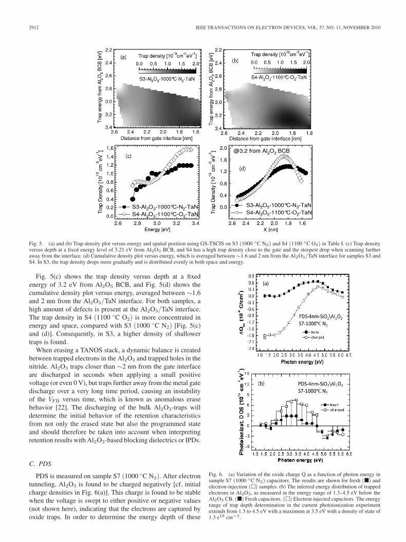
Fig. 4. Trap density plot versus energy and spatial position using SS-TSCIS on S1 (1000 ◦C N2) − S2 (1100 ◦C O2) in Table I. (a) For S1, most defects arelocalized in a horizontal band between 1.7 and 2.2 eV below the Al2O3 BCB. The average trap density is fitted with a Gaussian profile between 2 and 2.5 nm fromthe substrate interface to the main pick at ∼1.9 eV, and (c) the total trap density (integration under the Gaussian profile) results in 1.13 ± 0.02 × 10¹⁹ traps/cm−3
in the defect band. Similarly, (b) S2 shows a horizontal band between 1.4 and 2 eV, and (d) the defect density is concentrated at 1.65 eV, with a total trap densityof 1.94 ± 0.02 × 10¹⁹ traps/cm−3 in the defect band extracted with a Gaussian profile between 2.5 and 3 nm.
characterization measurements were not performed on a scaleto allow statistical analysis of the errors. However, a few repeatswere done to check the device variations and the measurementrepeatability. Specifically for TSCIS, sample-to-sample, wafer-to-wafer, and lot-to-lot variations were evaluated and shown tobe within acceptable margins (∼10%).
A. SS-TSCIS
SS-TSCIS is applied to samples S1 (1000 ◦C N2) and S2(1100 ◦C O2) listed in Table I. Fig. 4(a) and (b) shows the trapdensity map versus energy from the top of the Al2O3 BCB anddistance from the Si/SiO2 interface, respectively, in samples S1and S2. Fig. 4(c) and (d) shows the cumulative density plotversus energy, averaged in the Al2O3 bulk, together with aGaussian fit to the main density peak. For both samples, weclearly observe a defect band. These results are fully consistentwith trap depth extraction from retention measurements, whichpredicted a trap band of similar depths to be responsible forretention in floating-gate Flash memory with Al2O3 IPD [30].
In S1 (1000 ◦C N2), the peak value is fitted at ∼1.9 eV andthe width (fwhm) = 0.06 ± 0.02 eV. After integration of theGaussian distribution over energy, we find a bulk Al2O3 trapdensity in the defect band of 1.13 ± 0.02 × 10¹⁹ traps/cm−3.In S2 (1100 ◦C O2), the peak value is slightly shallower at
∼1.65 eV and the width (fwhm) = 0.10 ± 0.02 eV. The cor-responding bulk Al2O3 trap density after integration is 1.95 ±0.02 × 10¹⁹ traps/cm−3. We also observe an additional con-centration of traps below 2 eV for S1 and 1.8 eV for S2. Insummary, in sample S2, the defects are more concentrated in asharply defined defect band, whereas, in sample S1, the defectband is broader, which suggests that O2 PDA at 1100 ◦C resultsin the most complete crystallization of the Al2O3, comparedwith N2 PDA at 1000 ◦C. The band in both Fig. 4(a) and (b)is not perfectly horizontal when scanning in the Al2O3 bulk,due to either 1) an intermixing of Al2O3 with SiO2 or 2) thepresence of a large amount of traps at a deeper level. As wewill show in the succeeding sections, a second defect bandat deeper level indeed exists and can be charged in a freshdevice through the SiO2 layer that is ∼1 nm. Note that theleakage current through shallow defects has strong temperatureacceleration, drastically affecting charge loss in memory cellsat high temperatures [31].
B. GS-TSCIS
Fig. 5(a) and (b) shows the trap density obtained with GS-TSCIS versus energy from Al2O3 BCB and distance from thegate interface, respectively, in samples S3 (1000 ◦C N2) and S4(1100 ◦C O2) listed in Table I.
2912 IEEE TRANSACTIONS ON ELECTRON DEVICES, VOL. 57, NO. 11, NOVEMBER 2010
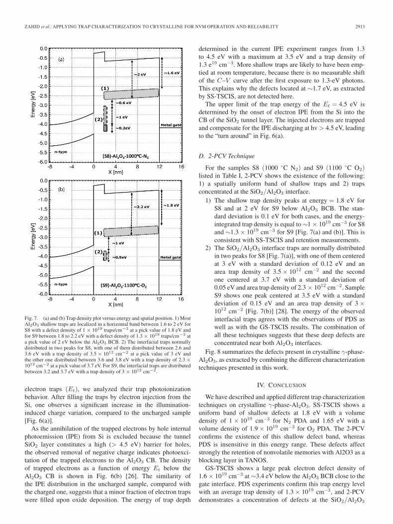
Fig. 5. (a) and (b) Trap density plot versus energy and spatial position using GS-TSCIS on S3 (1000 ◦C N2) and S4 (1100 ◦C O2) in Table I. (c) Trap densityversus depth at a fixed energy level of 3.21 eV from Al2O3 BCB, and S4 has a high trap density close to the gate and the steepest drop when scanning furtheraway from the interface. (d) Cumulative density plot versus energy, which is averaged between ∼1.6 and 2 nm from the Al2O3/TaN interface for samples S3 andS4. In S3, the trap density drops more gradually and is distributed evenly in both space and energy.
Fig. 5(c) shows the trap density versus depth at a fixedenergy of 3.2 eV from Al2O3 BCB, and Fig. 5(d) shows thecumulative density plot versus energy, averaged between ∼1.6and 2 nm from the Al2O3/TaN interface. For both samples, ahigh amount of defects is present at the Al2O3/TaN interface.The trap density in S4 (1100 ◦C O2) is more concentrated inenergy and space, compared with S3 (1000 ◦C N2) [Fig. 5(c)and (d)]. Consequently, in S3, a higher density of shallowertraps is found.
When erasing a TANOS stack, a dynamic balance is createdbetween trapped electrons in the Al2O3 and trapped holes in thenitride. Al2O3 traps closer than ∼2 nm from the gate interfaceare discharged in seconds when applying a small positivevoltage (or even 0 V), but traps further away from the metal gatedischarge over a very long time period, causing an instabilityof the VFB versus time, which is known as anomalous erasebehavior [22]. The discharging of the bulk Al2O3-traps willdetermine the initial behavior of the retention characteristicsfrom not only the erased state but also the programmed stateand should therefore be taken into account when interpretingretention results with Al2O3-based blocking dielectrics or IPDs.
C. PDS
PDS is measured on sample S7 (1000 ◦C N2). After electrontunneling, Al2O3 is found to be charged negatively [cf. initialcharge densities in Fig. 6(a)]. This charge is found to be stablewhen the voltage is swept to either positive or negative values(not shown here), indicating that the electrons are captured byoxide traps. In order to determine the energy depth of these
Fig. 6. (a) Variation of the oxide charge Q as a function of photon energy insample S7 (1000 ◦C N2) capacitors. The results are shown for fresh (�) andelectron-injection (�) samples. (b) The inferred energy distribution of trappedelectrons in Al2O3, as measured in the energy range of 1.3–4.5 eV below theAl2O3 CB. (�) Fresh capacitors. (�) Electron injected capacitors. The energyrange of trap depth determination in the current photoionization experimentextends from 1.3 to 4.5 eV with a maximum at 3.5 eV with a density of state of1.3 e19 cm−3.
ZAHID et al.: APPLYING TRAP CHARACTERIZATION TO CRYSTALLINE FOR NVM OPERATION AND RELIABILITY 2913
Fig. 7. (a) and (b) Trap density plot versus energy and spatial position. 1) MostAl2O3 shallow traps are localized in a horizontal band between 1.6 to 2 eV forS8 with a defect density of 1 × 10¹⁹ traps/cm−3 at a pick value of 1.8 eV andfor S9 between 1.8 to 2.2 eV with a defect density of 1.3 × 10¹⁹ traps/cm−3 ata pick value of 2 eV below the Al2O3 BCB. 2) The interfacial traps normallydistributed in two peaks for S8, with one of them distributed between 2.6 and3.6 eV with a trap density of 3.5 × 1012 cm−2 at a pick value of 3 eV andthe other one distributed between 3.6 and 3.8 eV with a trap density of 2.3 ×1012 cm−2 at a pick value of 3.7 eV. For S9, the interfacial traps are distributedbetween 3.2 and 3.7 eV with a trap density of 3 × 1012 cm−2.
electron traps (Et), we analyzed their trap photoionizationbehavior. After filling the traps by electron injection from theSi, one observes a significant increase in the illumination-induced charge variation, compared to the uncharged sample[Fig. 6(a)].
As the annihilation of the trapped electrons by hole internalphotoemission (IPE) from Si is excluded because the tunnelSiO2 layer constitutes a high (> 4.5 eV) barrier for holes,the observed removal of negative charge indicates photoexci-tation of the trapped electrons to the Al2O3 CB. The densityof trapped electrons as a function of energy Et below theAl2O3 CB is shown in Fig. 6(b) [26]. The similarity ofthe IPE distribution in the uncharged sample, compared withthe charged one, suggests that a minor fraction of electron trapswere filled upon oxide deposition. The energy of trap depth
determined in the current IPE experiment ranges from 1.3to 4.5 eV with a maximum at 3.5 eV and a trap density of1.3 e19 cm−3. More shallow traps are likely to have been emp-tied at room temperature, because there is no measurable shiftof the C–V curve after the first exposure to 1.3-eV photons.This explains why the defects located at ∼1.7 eV, as extractedby SS-TSCIS, are not detected here.
The upper limit of the trap energy of the Et = 4.5 eV isdetermined by the onset of electron IPE from the Si into theCB of the SiO2 tunnel layer. The injected electrons are trappedand compensate for the IPE discharging at hv > 4.5 eV, leadingto the “turn around” in Fig. 6(a).
D. 2-PCV Technique
For the samples S8 (1000 ◦C N2) and S9 (1100 ◦C O2)listed in Table I, 2-PCV shows the existence of the following:1) a spatially uniform band of shallow traps and 2) trapsconcentrated at the SiO2/Al2O3 interface.
1) The shallow trap density peaks at energy = 1.8 eV forS8 and at 2 eV for S9 below Al2O3 BCB. The stan-dard deviation is 0.1 eV for both cases, and the energy-integrated trap density is equal to ∼1 × 1019 cm−3 for S8and ∼1.3 × 1019 cm−3 for S9 [Fig. 7(a) and (b)]. This isconsistent with SS-TSCIS and retention measurements.
2) The SiO2/Al2O3 interface traps are normally distributedin two peaks for S8 [Fig. 7(a)], with one of them centeredat 3 eV with a standard deviation of 0.12 eV and anarea trap density of 3.5 × 1012 cm−2 and the secondone centered at 3.7 eV with a standard deviation of0.05 eV and area trap density of 2.3 × 1012 cm−2. SampleS9 shows one peak centered at 3.5 eV with a standarddeviation of 0.15 eV and an area trap density of 3 ×1012 cm−2 [Fig. 7(b)] [28]. The energy of the observedinterfacial traps agrees with the observations of PDS aswell as with the GS-TSCIS results. The combination ofall these techniques suggests that these deep defects areconcentrated near both Al2O3 interfaces.
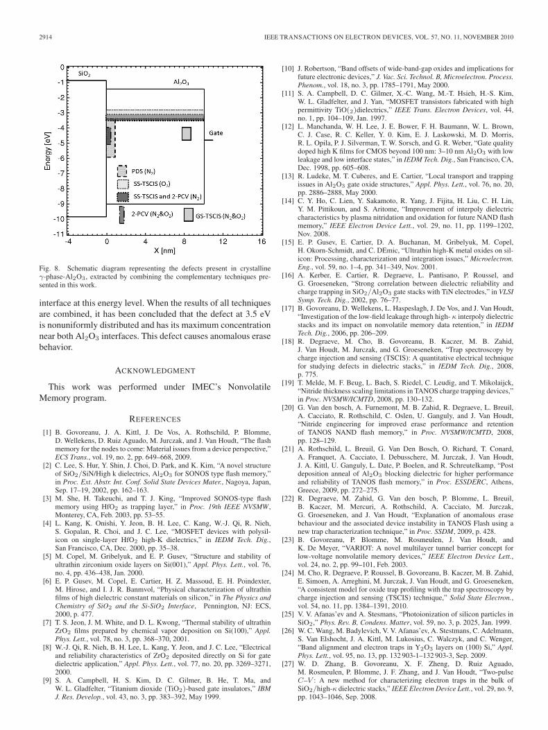
Fig. 8 summarizes the defects present in crystalline γ-phase-Al2O3, as extracted by combining the different characterizationtechniques presented in this work.
IV. CONCLUSION
We have described and applied different trap characterizationtechniques on crystalline γ-phase-Al2O3. SS-TSCIS shows auniform band of shallow defects at 1.8 eV with a volumedensity of 1 × 1019 cm−3 for N2 PDA and 1.65 eV with avolume density of 1.9 × 1019 cm−3 for O2 PDA. The 2-PCVconfirms the existence of this shallow defect band, whereasPDS is insensitive in this energy range. These defects affectstrongly the retention of nonvolatile memories with Al2O3 as ablocking layer in TANOS.
GS-TSCIS shows a large peak electron defect density of1.6 × 1019 cm−3 at ∼3.4 eV below the Al2O3 BCB close to thegate interface. PDS experiments confirm this trap energy levelwith an average trap density of 1.3 × 1019 cm−3, and 2-PCVdemonstrates a concentration of defects at the SiO2/Al2O3
2914 IEEE TRANSACTIONS ON ELECTRON DEVICES, VOL. 57, NO. 11, NOVEMBER 2010
Fig. 8. Schematic diagram representing the defects present in crystallineγ-phase-Al2O3, extracted by combining the complementary techniques pre-sented in this work.
interface at this energy level. When the results of all techniquesare combined, it has been concluded that the defect at 3.5 eVis nonuniformly distributed and has its maximum concentrationnear both Al2O3 interfaces. This defect causes anomalous erasebehavior.
ACKNOWLEDGMENT
This work was performed under IMEC’s NonvolatileMemory program.
REFERENCES
[1] B. Govoreanu, J. A. Kittl, J. De Vos, A. Rothschild, P. Blomme,D. Wellekens, D. Ruiz Aguado, M. Jurczak, and J. Van Houdt, “The flashmemory for the nodes to come: Material issues from a device perspective,”ECS Trans., vol. 19, no. 2, pp. 649–668, 2009.
[2] C. Lee, S. Hur, Y. Shin, J. Choi, D. Park, and K. Kim, “A novel structureof SiO2/SiN/High k dielectrics, Al2O3 for SONOS type flash memory,”in Proc. Ext. Abstr. Int. Conf. Solid State Devices Mater., Nagoya, Japan,Sep. 17–19, 2002, pp. 162–163.
[3] M. She, H. Takeuchi, and T. J. King, “Improved SONOS-type flashmemory using HfO2 as trapping layer,” in Proc. 19th IEEE NVSMW,Monterey, CA, Feb. 2003, pp. 53–55.
[4] L. Kang, K. Onishi, Y. Jeon, B. H. Lee, C. Kang, W.-J. Qi, R. Nieh,S. Gopalan, R. Choi, and J. C. Lee, “MOSFET devices with polysil-icon on single-layer HfO2 high-K dielectrics,” in IEDM Tech. Dig.,San Francisco, CA, Dec. 2000, pp. 35–38.
[5] M. Copel, M. Gribelyuk, and E. P. Gusev, “Structure and stability ofultrathin zirconium oxide layers on Si(001),” Appl. Phys. Lett., vol. 76,no. 4, pp. 436–438, Jan. 2000.
[6] E. P. Gusev, M. Copel, E. Cartier, H. Z. Massoud, E. H. Poindexter,M. Hirose, and I. J. R. Banmvol, “Physical characterization of ultrathinfilms of high dielectric constant materials on silicon,” in The Physics andChemistry of SiO2 and the Si-SiO2 Interface, Pennington, NJ: ECS,2000, p. 477.
[7] T. S. Jeon, J. M. White, and D. L. Kwong, “Thermal stability of ultrathinZrO2 films prepared by chemical vapor deposition on Si(100),” Appl.Phys. Lett., vol. 78, no. 3, pp. 368–370, 2001.
[8] W.-J. Qi, R. Nieh, B. H. Lee, L. Kang, Y. Jeon, and J. C. Lee, “Electricaland reliability characteristics of ZrO2 deposited directly on Si for gatedielectric application,” Appl. Phys. Lett., vol. 77, no. 20, pp. 3269–3271,2000.
[9] S. A. Campbell, H. S. Kim, D. C. Gilmer, B. He, T. Ma, andW. L. Gladfelter, “Titanium dioxide (TiO2)-based gate insulators,” IBMJ. Res. Develop., vol. 43, no. 3, pp. 383–392, May 1999.
[10] J. Robertson, “Band offsets of wide-band-gap oxides and implications forfuture electronic devices,” J. Vac. Sci. Technol. B, Microelectron. Process.Phenom., vol. 18, no. 3, pp. 1785–1791, May 2000.
[11] S. A. Campbell, D. C. Gilmer, X.-C. Wang, M.-T. Hsieh, H.-S. Kim,W. L. Gladfelter, and J. Yan, “MOSFET transistors fabricated with highpermittivity TiO(2)dielectrics,” IEEE Trans. Electron Devices, vol. 44,no. 1, pp. 104–109, Jan. 1997.
[12] L. Manchanda, W. H. Lee, J. E. Bower, F. H. Baumann, W. L. Brown,C. J. Case, R. C. Keller, Y. 0. Kim, E. J. Laskowski, M. D. Morris,R. L. Opila, P. J. Silverman, T. W. Sorsch, and G. R. Weber, “Gate qualitydoped high K films for CMOS beyond 100 nm: 3–10 nm Al2O3 with lowleakage and low interface states,” in IEDM Tech. Dig., San Francisco, CA,Dec. 1998, pp. 605–608.
[13] R. Ludeke, M. T. Cuberes, and E. Cartier, “Local transport and trappingissues in Al2O3 gate oxide structures,” Appl. Phys. Lett., vol. 76, no. 20,pp. 2886–2888, May 2000.
[14] C. Y. Ho, C. Lien, Y. Sakamoto, R. Yang, J. Fijita, H. Liu, C. H. Lin,Y. M. Pittikoun, and S. Aritome, “Improvement of interpoly dielectriccharacteristics by plasma nitridation and oxidation for future NAND flashmemory,” IEEE Electron Device Lett., vol. 29, no. 11, pp. 1199–1202,Nov. 2008.
[15] E. P. Gusev, E. Cartier, D. A. Buchanan, M. Gribelyuk, M. Copel,H. Okorn-Schmidt, and C. DEmic, “Ultrathin high-K metal oxides on sil-icon: Processing, characterization and integration issues,” Microelectron.Eng., vol. 59, no. 1–4, pp. 341–349, Nov. 2001.
[16] A. Kerber, E. Cartier, R. Degraeve, L. Pantisano, P. Roussel, andG. Groeseneken, “Strong correlation between dielectric reliability andcharge trapping in SiO2/Al2O3 gate stacks with TiN electrodes,” in VLSISymp. Tech. Dig., 2002, pp. 76–77.
[17] B. Govoreanu, D. Wellekens, L. Haspeslagh, J. De Vos, and J. Van Houdt,“Investigation of the low-field leakage through high- κ interpoly dielectricstacks and its impact on nonvolatile memory data retention,” in IEDMTech. Dig., 2006, pp. 206–209.
[18] R. Degraeve, M. Cho, B. Govoreanu, B. Kaczer, M. B. Zahid,J. Van Houdt, M. Jurczak, and G. Groeseneken, “Trap spectroscopy bycharge injection and sensing (TSCIS): A quantitative electrical techniquefor studying defects in dielectric stacks,” in IEDM Tech. Dig., 2008,p. 775.
[19] T. Melde, M. F. Beug, L. Bach, S. Riedel, C. Leudig, and T. Mikolaijck,“Nitride thickness scaling limitations in TANOS charge trapping devices,”in Proc. NVSMW/ICMTD, 2008, pp. 130–132.
[20] G. Van den bosch, A. Furnemont, M. B. Zahid, R. Degraeve, L. Breuil,A. Cacciato, R. Rothschild, C. Oslen, U. Ganguly, and J. Van Houdt,“Nitride engineering for improved erase performance and retentionof TANOS NAND flash memory,” in Proc. NVSMW/ICMTD, 2008,pp. 128–129.
[21] A. Rothschild, L. Breuil, G. Van Den Bosch, O. Richard, T. Conard,A. Franquet, A. Cacciato, I. Debusschere, M. Jurczak, J. Van Houdt,J. A. Kittl, U. Ganguly, L. Date, P. Boelen, and R. Schreutelkamp, “Postdeposition anneal of Al2O3 blocking dielectric for higher performanceand reliability of TANOS flash memory,” in Proc. ESSDERC, Athens,Greece, 2009, pp. 272–275.
[22] R. Degraeve, M. Zahid, G. Van den bosch, P. Blomme, L. Breuil,B. Kaczer, M. Mercuri, A. Rothschild, A. Cacciato, M. Jurczak,G. Groeseneken, and J. Van Houdt, “Explanation of anomalous erasebehaviour and the associated device instability in TANOS Flash using anew trap characterization technique,” in Proc. SSDM, 2009, p. 428.
[23] B. Govoreanu, P. Blomme, M. Rosmeulen, J. Van Houdt, andK. De Meyer, “VARIOT: A novel multilayer tunnel barrier concept forlow-voltage nonvolatile memory devices,” IEEE Electron Device Lett.,vol. 24, no. 2, pp. 99–101, Feb. 2003.
[24] M. Cho, R. Degraeve, P. Roussel, B. Govoreanu, B. Kaczer, M. B. Zahid,E. Simoen, A. Arreghini, M. Jurczak, J. Van Houdt, and G. Groeseneken,“A consistent model for oxide trap profiling with the trap spectroscopy bycharge injection and sensing (TSCIS) technique,” Solid State Electron.,vol. 54, no. 11, pp. 1384–1391, 2010.
[25] V. V. Afanas’ev and A. Stesmans, “Photoionization of silicon particles inSiO2,” Phys. Rev. B, Condens. Matter, vol. 59, no. 3, p. 2025, Jan. 1999.
[26] W. C. Wang, M. Badylevich, V. V. Afanas’ev, A. Stestmans, C. Adelmann,S. Van Elshocht, J. A. Kittl, M. Lukosius, C. Walczyk, and C. Wenger,“Band alignment and electron traps in Y2O3 layers on (100) Si,” Appl.Phys. Lett., vol. 95, no. 13, pp. 132 903-1–132 903-3, Sep. 2009.
[27] W. D. Zhang, B. Govoreanu, X. F. Zheng, D. Ruiz Aguado,M. Rosmeulen, P. Blomme, J. F. Zhang, and J. Van Houdt, “Two-pulseC–V : A new method for characterizing electron traps in the bulk ofSiO2/high-κ dielectric stacks,” IEEE Electron Device Lett., vol. 29, no. 9,pp. 1043–1046, Sep. 2008.
ZAHID et al.: APPLYING TRAP CHARACTERIZATION TO CRYSTALLINE FOR NVM OPERATION AND RELIABILITY 2915
[28] D. R. Aguado, B. Govoreanu, W. D. Zhang, M. Jurczak, K. De Meyer,and J. Van Houdt, “A novel trapping/detrapping model for defect profilingin high-k materials using the two-pulse capacitance–voltage technique,”IEEE Trans. Electron Devices, vol. 57, no. 10, pp. 2726–2735, Oct. 2010.
[29] M. Toledano-Luque, R. Degraeve, M. B. Zahid, B. Kaczer, J. Kittl,M. Jurczak, G. Groeseneken, and J. Van Houdt, “Resolving fast VTHtransients after program/erase of flash memory stacks and their relationto electron and hole defects,” in IEDM Tech. Dig., 2009, p. 749.
[30] B. Govoreanu, R. Degraeve, J. Van Houdt, M. Jurczak, B. Govoreanu,R. Degraeve, J. Van Houdt, and M. Jurczak, “Statistical investigation ofthe floating gate memory cell leakage through high- k interpoly dielectricsand its impact on scalability and reliability,” in IEDM Tech. Dig., 2008,pp. 353–356.
[31] B. Govoreanu and J. Van Houdt, “On the roll-off of the activation energyplot in high-temperature flash memory retention tests and its impact onthe reliability assessment,” IEEE Electron Device Lett., vol. 29, no. 2,pp. 177– 179, Feb. 2008.
[32] M. B. Zahid, R. Degraeve, M. J. Cho, L. Pantisano, D. R. Aguado,J. Van Houdt, G. Groeseneken, and M. Jurczak, “Defect profiling inthe SiO2/Al2O3 interface using variable tcharge − tdischarge amplitudecharge pumping (VT2ACP),” in Proc. 47th Annu. IEEE IRPS, 2009,pp. 21–25.
[33] D. A. Mehta, S. R. Butler, and F. J. Feigl, “Electronic charge trapping inchemical vapor-deposited thin films of Al2O3 on silicon,” J. Appl. Phys.,vol. 43, no. 11, pp. 4631–4638, Nov. 1972.
[34] M. C. Kim, S. Kim, S.-H. Choi, K. Belay, R. G. Elliman, andS. P. Russo, “Nonvolatile-memory characteristics of AlO-implantedAl2O3,” IEEE Electron Device Lett., vol. 30, no. 8, pp. 837–839,Aug. 2009.
Mohammed B. Zahid received the Diplome Uni-versitaire de Technologie in electronics and com-puting from the University of Technologies (IUT),Cachan, France, in 2001 and the Bachelor’s degreein electrical engineering, the Master’s degree in mi-croelectronics, and the Ph.D. degree in “Character-ization of high-k layers as the gate dielectric forMOSFETs” from Liverpool John Moores University(LJMU), Liverpool, U.K., in 2002, 2003, and 2007,respectively.
He was a Postdoctoral Researcher with the groupof Device Reliability and Electrical Characterization (DRE), InteruniversityMicroelectronics Center (IMEC), Leuven, Belgium, where he is currentlyworking on high-power-based GaN devices and characterization of nonvolatilememory (NVM) with alternative high-k dielectrics. His research interestsinclude the technology and novel electrical characterization techniques andreliability for NVM, flash memory, and GaN high-power devices.
Daniel Ruiz Aguado was born in Valladolid, Spain,on August 30, 1980. He received the B.S. degreein telecommunications engineering and the M.S.degree in electronics engineering from ValladolidUniversity, in 2002 and 2005, respectively. He iscurrently working toward the Ph.D. degree at IMEC-Belgium, Leuven, Belgium, under the supervision ofthe Katholieke Universiteit of Leuven, Leuven.
He is also with the ESAT Department, KatholiekeUniversiteit Leuven. His research interests includethe characterization of high-k dielectrics for new
nonvolatile memory applications.
R. Degraeve, photograph and biography not available at the time of publication.
W. C. Wang, photograph and biography not available at the time of publication.
Bogdan Govoreanu (M’05) received the Lic.-Eng.and M.Sc. degrees in electronics from the TechnicalUniversity (TU) of Bucharest, Romania, in 1995 and1996, respectively, and the Ph.D. degree in appliedsciences from Katholieke Universiteit Leuven (KULeuven), Leuven, Belgium, in 2004, for his researchon novel nonvolatile memory device concepts carriedout at the Interuniversity Microelectronics Center(IMEC), Leuven.
In 1996, he was a Research Assistant with theElectronics Department (ED), TU Bucharest. From
1997 to 1998, he was a Visiting Researcher with IMEC. From 1998 to 1999,he was a Teaching Assistant (TU Bucharest/ED). From 1999 to 2000, he was aGuest Researcher with KU Leuven/IMEC. He is currently with IMEC, wherehe has been working on various research areas, including modeling, charac-terization, and reliability of nonvolatile/Flash memory, high-k dielectric, andtechnology computer-aided design methodologies for empirical model buildingand optimization techniques. He has published more than 60 research papersin internationally recognized journals and conference proceedings. He is theholder of several European and U.S. patent applications. His current researchinterests include emerging resistance switching-based memory concepts.
María Toledano-Luque was born in Madrid, Spain,in 1980. She received the M.Sc. degree in electri-cal engineering, the M.Sc. degree in physics, andthe Ph.D. degree from the Universidad Complutensede Madrid (UCM), Madrid, Spain, in 2003, 2009,and 2008.
In 2003, she became a member of the Thin Filmsand Microelectronics research group, UCM. In 2007,she joined the Departamento Física Aplicada III,UCM, as an Assistant Professor. She is currentlya Postdoctoral Researcher with IMEC, Leuven,
Belgium, working in the field of advance electrical characterization.
V. V. Afanas’ev, photograph and biography not available at the time ofpublication.
2916 IEEE TRANSACTIONS ON ELECTRON DEVICES, VOL. 57, NO. 11, NOVEMBER 2010
Jan Van Houdt (SM’02) was born in Leuven,Belgium, on June 20, 1963. He received the M.Sc.degree in electrical and mechanical engineering andthe Ph.D. degree in applied sciences from KatholiekeUniversiteit Leuven, in 1987 and 1994, respectively.His M.S. thesis dealt with the degradation of short-channel MOS transistors under hot-carrier injectionconditions. His Ph.D. work concentrated on thephysics and characteristics of HIMOS Flash memorydevices.
After his M.S. thesis, he joined the InteruniversityMicro-Electronics Center (IMEC), Leuven. In 1990, he invented the HighInjection MOS (HIMOS) transistor, which is a novel fast-programmable FlashEEPROM cell that has led to a high-performance cost-effective nonvolatilememory technology, on which he holds numerous international patents. In1996, he became responsible for the development and dissemination of Flashmemory technology based on IMEC’s proprietary concepts, including thelicensing and the transfer of these technologies toward 4 industrial prod-uct lines. Since 1999, he has been managing the memory group at IMEC.Since 2000, he has been managing IMEC’s Industrial Affiliation Program onAdvanced Memory Technology and expanded it to become one of IMEC’slargest research programs today. His research interests are the physics of semi-
conductor devices; hot-carrier injection and degradation phenomena in MOSstructures; thin dielectrics; modeling and optimization of floating-gate andnitride nonvolatile memory devices; and physics, reliability, and design aspectsof memories in general. He has published more than 160 papers in internationaljournals, written two book chapters, and accumulated more than 140 conferenceproceeding contributions (including more than 25 invitations and five BestPaper Awards). He is the holder of more than 50 patent applications worldwidein the area of nonvolatile memories, of which 27 patents have been granted sofar. He serves (or served) on the program and/or organizational committees ofthe IEEE Nonvolatile Semiconductor Memory Workshop; the IEEE ReliabilityPhysics Symposium; the European Solid-State Device Research Conference;the International Conference on Memory Technology and Design; the IEEEInternational Workshop on Memory Technology, Design and Testing (Taiwan);the Solid-State Devices and Materials conference; the MRS symposium onnonvolatile memory technologies; the International Memory Workshop; theIEEE International Electron Devices Meeting; and the IEEE SemiconductorInterface Specialists Conference. In 2007, he was the General Chairman of theInternational Conference on Memory Technology and Design.
Dr. Van Houdt was the recipient of the Best Student Paper Award at the 22ndEuropean Solid-State Device Research Conference in 1992 and the ScientificAward of the Royal Academy for Science, Literature and Fine Arts of Belgiumin 1995.