Analysis of correlation between electrical and infrared optical properties of anatase Nb doped TiO2...
6
Analysis of correlation between electrical and infrared optical properties of anatase Nb doped TiO 2 films Weitao Su a, * , Kaixin Song b , Dexuan Huo a , Bin Li c,1 a Institute of Materials Physics, Hangzhou Dianzi University, 2nd Road, 310018 Hangzhou, China b College of Electronics and Information, Hangzhou Dianzi University, 310018 Hangzhou, China c Shanghai Institute of Technical Physics, Chinese Academic of Science, 200083 Shanghai, China article info Article history: Received 6 April 2012 Received in revised form 19 September 2012 Accepted 2 October 2012 Available online 23 October 2012 Keywords: Anatase Nb:TiO 2 films Ellipsometry Electrical inhomogeneity Infrared reflection abstract Optical and electrical analysis are required to clarify infrared reflection behavior of anatase Nb doped TiO 2 (NTO) films, a novel transparent conductive oxide (TCO). In this paper, UVevis-near infrared transmission spectrum, Fourier transformed infrared (FTIR) reflection and ellipsometry analysis are conducted on anatase NTO films (Nb doping concentration: 6, 4 and 2 at%) deposited by pulse laser deposition (PLD). NTO samples show good transparency from 400 nm to 1000 nm, but no obvious plasmon induced high IR reflection even when wavelength >3000 nm. Assuming inhomogeneous resistivity (r) and mean scattering time (s) along film thickness, dielectric constants (ε r , ε i ) and optical constants (n, k) are extracted by fitting spectroscopic ellipsometry using Code-Lorentz (CL) & Drude exponential model. It is shown that unique optical constants and small s (1.1e2.6 fs) intrinsically prevent NTO to be high infrared reflective TCO. Ó 2012 Elsevier B.V. All rights reserved. 1. Introduction Anatase Nb doped TiO 2 (NTO) film, as a novel transparent conductive oxide (TCO) with high doping efficiency and carrier concentration [1e3], has drew considerable attention from researchers all over the world. According to Y. Furubayashi’s report [3], even small dose of Nb atom is able to excite high carrier concentration in the order of magnitude of 10 20 e10 21 cm 3 . In recent years, anatase NTO films with low resistivity have been successfully deposited on various substrates, such as LaAlO 3 [2,4], fused silica [5] and glass substrates [6], etc. The lowest resistivity of NTO in references [1e6] is w2 10 4 U cm, which is comparable to ITO [7] and doped ZnO films [8], while transparency is still preserved. Many researches propose NTO’s potential applications in solar cells, [9] flat panel display, [4,6] photocatalysts, [10] etc. It is well known that, for TCO, the plasmon resonance frequency u p can be described as [11] u p ¼ e 2 N f ε 0 ε N m * ! 1=2 (1) in which e, ε 0 , ε and m * are electron charge, permittivity, high frequency dielectric constant and effective mass, respectively. Although m * varies with different carrier concentrations, m * is only doubled if carrier concentration increases from 10 19 to 10 21 cm 3 [3,12]. If carrier concentration only varies within one order of magnitude, the contribution of m * in equation (1) coarsely keeps constant and u p only increases with square root of carrier concentration. Granqvist [7] demonstrates u p clearly blue shifts if N f rises from 10 20 to 10 21 cm 3 . It is expected that, the similarities of u p and infrared reflective behavior will be observed for NTO with r w10 4 U cm and N f w10 21 cm 3 at room temperature. However, most of existing evidences [5,13,14] support that IR reflection of NTO films, even for films with lowest resistivity and larger thick- ness (beyond 200 nm), is much poor than that of ITO [7] and doped ZnO films [8]. Correlation between optical and electric properties needs to be further clarified to reveal the intrinsic correlation. Toward this end, ellipsometry, transmission and reflection spec- trum measurements and calculations are employed to quantify IR reflection and absorption, and their possible relation to electrical properties. This work presents that unique optical constants, and low s, as well as induced low carrier mobility, are dominant factors inhibiting NTO’s IR reflective performance. 2. Experimental details Pulse laser ablation on sintered NTO ceramic targets (Nb content: 2 at%, 4 at% and 6 at%), deposition at ambient condition, * Corresponding author. Tel./fax: þ86 571 87713537. E-mail addresses: [email protected] (W. Su), [email protected] (B. Li). 1 Tel./fax: þ86 21 25051308. Contents lists available at SciVerse ScienceDirect Current Applied Physics journal homepage: www.elsevier.com/locate/cap 1567-1739/$ e see front matter Ó 2012 Elsevier B.V. All rights reserved. http://dx.doi.org/10.1016/j.cap.2012.10.004 Current Applied Physics 13 (2013) 556e561
Transcript of Analysis of correlation between electrical and infrared optical properties of anatase Nb doped TiO2...
at SciVerse ScienceDirect
Current Applied Physics 13 (2013) 556e561
Contents lists available
Current Applied Physics
journal homepage: www.elsevier .com/locate/cap
Analysis of correlation between electrical and infrared optical propertiesof anatase Nb doped TiO2 films
Weitao Su a,*, Kaixin Song b, Dexuan Huo a, Bin Li c,1
a Institute of Materials Physics, Hangzhou Dianzi University, 2nd Road, 310018 Hangzhou, ChinabCollege of Electronics and Information, Hangzhou Dianzi University, 310018 Hangzhou, Chinac Shanghai Institute of Technical Physics, Chinese Academic of Science, 200083 Shanghai, China
a r t i c l e i n f o
Article history:Received 6 April 2012Received in revised form19 September 2012Accepted 2 October 2012Available online 23 October 2012
Keywords:Anatase Nb:TiO2 filmsEllipsometryElectrical inhomogeneityInfrared reflection
* Corresponding author. Tel./fax: þ86 571 8771353E-mail addresses: [email protected] (W. Su),
1 Tel./fax: þ86 21 25051308.
1567-1739/$ e see front matter � 2012 Elsevier B.V.http://dx.doi.org/10.1016/j.cap.2012.10.004
a b s t r a c t
Optical and electrical analysis are required to clarify infrared reflection behavior of anatase Nb dopedTiO2 (NTO) films, a novel transparent conductive oxide (TCO). In this paper, UVevis-near infraredtransmission spectrum, Fourier transformed infrared (FTIR) reflection and ellipsometry analysis areconducted on anatase NTO films (Nb doping concentration: 6, 4 and 2 at%) deposited by pulse laserdeposition (PLD). NTO samples show good transparency from 400 nm to 1000 nm, but no obviousplasmon induced high IR reflection even when wavelength >3000 nm. Assuming inhomogeneousresistivity (r) and mean scattering time (s) along film thickness, dielectric constants (εr, εi) and opticalconstants (n, k) are extracted by fitting spectroscopic ellipsometry using Code-Lorentz (CL) & Drudeexponential model. It is shown that unique optical constants and small s (1.1e2.6 fs) intrinsically preventNTO to be high infrared reflective TCO.
� 2012 Elsevier B.V. All rights reserved.
1. Introduction in which e, ε0, ε and m* are electron charge, permittivity, high
Anatase Nb doped TiO2 (NTO) film, as a novel transparentconductive oxide (TCO) with high doping efficiency and carrierconcentration [1e3], has drew considerable attention fromresearchers all over the world. According to Y. Furubayashi’sreport [3], even small dose of Nb atom is able to excitehigh carrier concentration in the order of magnitude of1020e1021 cm�3. In recent years, anatase NTO films with lowresistivity have been successfully deposited on varioussubstrates, such as LaAlO3 [2,4], fused silica [5] and glasssubstrates [6], etc. The lowest resistivity of NTO in references[1e6] is w2 � 10�4 U cm, which is comparable to ITO [7] anddoped ZnO films [8], while transparency is still preserved. Manyresearches propose NTO’s potential applications in solar cells,[9] flat panel display, [4,6] photocatalysts, [10] etc.
It is well known that, for TCO, the plasmon resonance frequencyup can be described as [11]
up ¼
e2Nf
ε0εNm*
!1=2
(1)
[email protected] (B. Li).
All rights reserved.
frequency dielectric constant and effective mass, respectively.Although m* varies with different carrier concentrations, m* is
only doubled if carrier concentration increases from 1019 to1021 cm�3 [3,12]. If carrier concentration only varies within oneorder of magnitude, the contribution of m* in equation (1) coarselykeeps constant and up only increases with square root of carrierconcentration. Granqvist [7] demonstrates up clearly blue shifts ifNf rises from 1020 to 1021 cm�3. It is expected that, the similarities ofup and infrared reflective behavior will be observed for NTO with r
w10�4 U cm and Nf w1021 cm�3 at room temperature. However,most of existing evidences [5,13,14] support that IR reflection ofNTO films, even for films with lowest resistivity and larger thick-ness (beyond 200 nm), is much poor than that of ITO [7] and dopedZnO films [8]. Correlation between optical and electric propertiesneeds to be further clarified to reveal the intrinsic correlation.Toward this end, ellipsometry, transmission and reflection spec-trum measurements and calculations are employed to quantify IRreflection and absorption, and their possible relation to electricalproperties. This work presents that unique optical constants, andlow s, as well as induced low carrier mobility, are dominant factorsinhibiting NTO’s IR reflective performance.
2. Experimental details
Pulse laser ablation on sintered NTO ceramic targets (Nbcontent: 2 at%, 4 at% and 6 at%), deposition at ambient condition,
W. Su et al. / Current Applied Physics 13 (2013) 556e561 557
and subsequently high vacuum (<10�4 Pa) annealing at 500 �Cwere used as typical growth procedures for NTO films. Duringpulse laser ablation process, laser power and frequency were keptat 300 mJ and 5 Hz, respectively. The deposition rate was kept at1.5 nm/min. Oxygen partial pressure of 0.5 Pa was found to be theoptimum condition for low resistivity anatase NTO films. As-deposited oxygen-rich samples are much more conductive afterannealing, which indicates doping of Nb may be compensated byrich oxygen ions carrying negative charge. Three thicker NTO films(about 280 nm, Nb: 6 at%, 4 at% and 2 at%) were deposited atoxygen pressure of 0.5 Pa and annealed at 500 �C for 60 min. XRDand four-probe sheet resistance measurement were used toinvestigate the crystallographic structure and sheet resistance,respectively. Transmission spectra were measured from 200 nm to2500 nm at normal incidence. Fourier transformed infrared (FTIR)reflection spectra were measured from 5000 cm�1 to 400 cm�1
(fresh Ag mirror as reference, incident angle ¼ 30�). Note thatnoise peak at 2200 cm�1 owning to CO2 correction should beomitted. Ellipsometry spectra from 300 nm to 2500 nm weremeasured on VASE (J. A. Woollam) system at 55�and 75�.
500 1000 1500 2000 25000
10
20
30
40
Ψ55°
Ψ75°
Δ75°
Wavelength(nm)
Ψ(°
)
Δ55°
solid: measured ;dash: exponential grade;dot: simple grade; dash dot: bilayer model 0
60
120
180
Δη°η
a
b
ρ
ρ
ρ
ρ
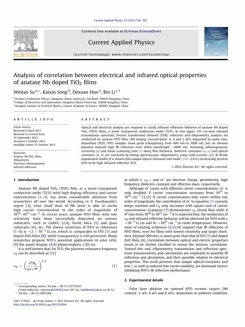
Fig. 1. (a) Schematic of bilayer and exponential model used in the fitting process ofNTO and (b) calculated (J, D) with different models.
3. Ellipsometry modeling and analysis
Similar to ITO [15] and Al doped ZnO [16] films, NTOalso shows absorption in UV wavelength and plasmon-related electron absorption from visible to infrared. In thispaper, Code-Lorentz (CL) oscillator model is used to getgood fitness for band edge and “urbach tail” absorptioncaused by high concentration of dopant. Drude model isadopted to fit the plasmon-related absorption. Hence totaldielectric function is expressed as sum of Code-Lorentz andDrude mode:
εðEÞ ¼ εr þ iεi ¼ εCL þ εD (2)
here εr and εi are the real and imaginary part of dielectric function,respectively; εCL and εD are dielectric contribution from Code-Lorentz and Drude model, respectively.
In Code-Lorentz model, complex dielectric function is expressedas [17]
εCLðEÞ ¼ ε1 þ iε2 (3)
where ε1 and ε2 are real and imaginary part of dielectric function,respectively.
In equation (3), if E > Eg þ Et:
ε2 ¼ GðEÞLðEÞ ¼�E � Eg
�2�E � Eg
�2þE2p$
264 AEoG�E2 � E2o
�2þG2E2
375 (4)
For a simple expression, let E1 ¼ G(E)L(E). If 0 < E < Eg þ Et then
ε2 ¼ E1Eexp
�E � Eg � Et
Em
�(5)
In equations (4) and (5), A is amplitude, Eo is peak transitionenergy, Eg is band gap, Eu represents the extension of broad-ening, Ep is transition energy for absorption onset, Et istransition energy between urbach tail and band-to-bandtransitions [18].
Real part ε1 in equation (3) is calculated from ε2 usingKramerseKronig relationship [11]
ε1 ¼ 2PZN
xε2ðxÞ dx (6)
p0x2 � E2
where P is the principal value of integral [11]
PZN0
dxh lims/0
0B@ ZE�s
0
dxþZN
Eþs
dx
1CA (7)
Drude model used in this paper is expressed as [17]
εDðEÞ ¼ � h2
ε0r�sE2 þ iZE
� (8)
where ε0 is dielectric constant; r is resistivity of film; s is meancarrier scattering time and h is Plank constant.
In fitting process, εN, A, Eg, E0, Em, Ep, Et, G, r and s are used asfitting parameters to get best approaching to measured spectra. Forthinner films (thickness <100 nm) deposited at different oxygenpressures, simple CL and Drude oscillator model without grade isvery efficient. Mean square error (MSE) below 5 is obtained inseveral steps. However, single oscillator model cannot convergewell for thicker films (thickness about 300 nm), which suggeststhat thicker films may have inhomogeneous electrical propertiesalong the film thickness, like previous study for ITO and ZnO films[15,16].
As a preliminary consideration, we construct a bilayer model,with low resistivity layer on top surface and higher resistivity layerat the bottom, as demonstrated in Fig. 1(a). It is surprisingly foundthat generated andmeasured (J, D) can agree with each other verywell for both angles, as shown in Fig. 1(b). Although it is onlyapproximation, the bilayer model is much better than simple grademode in Fig. 1(b). Herein, we presume there is an exponentialgradient of resistivity along film thickness when we select
W. Su et al. / Current Applied Physics 13 (2013) 556e561558
dispersion model (Fig. 1(a)). In the fitting process, only r and s areexponentially graded. r takes r ¼ r0e
G1x and s takes s ¼ s0eG2x,where G1 and G2 are gradient percentage, while x is the thicknessratio from filmesubstrate interface (x¼ 0) to the top surface (x¼ 1).The variation of G1 and G2 are limited between 0 and -0.8 toguarantee that generated grade profiles of r0 and s0 follow thermaldiffusion mechanism. Better fitness between calculated andmeasured J and D for NTO (doped with 6 at% Nb) is demonstratedin Fig. 1(b), which supports the reasonability of this model.Attempts to use gradient for other parameters in CL model, such asεN, A, Eg, E0, Em, Ep, Et, G, fail to provide more improvement, which isnot shown in this paper.
4. Results and discussions
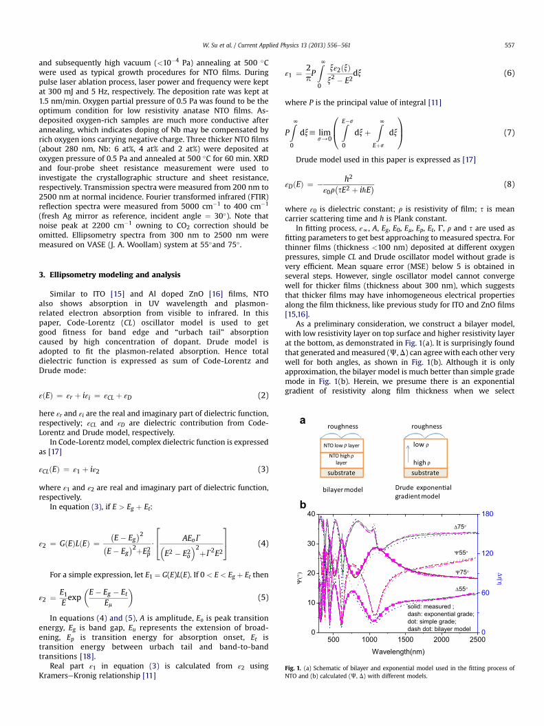
Fig. 2(a) presents XRD results for films deposited at differentoxygen pressures. At 0.1 Pa O2 pressure, the film shows typicalrutile structure with (200) growth orientation. Sheet resistance ofrutile TiO2 is in the order of MU/,. The sheet resistance for anataseTiO2 films, which are deposited at 0.5 Pa and 1 Pa, are 230 U/, and2 � 105 U/,, respectively. Our results confirm that the structureand resistivity of NTO films are all very sensitive to oxygen pressure.Low resistance anatase NTO films can only be deposited in narrowoxygen pressure “window” around 0.5 Pa. Anatase TiO2 films withdifferent Nb doping concentrations (6, 4 and 2 at%), shown inFig. 2(b), have similar (101) growth orientation, while peak inten-sity of (004) increases with decreasing Nb concentration, whichindicates poor film quality. Sheet resistance in the centre of threesamples are 79 U/,(6 at%), 57 U/,(4 at%) and 26 U/,(2 at%),respectively. The possible reasons that 2 at% NTO sample, with poorcrystal structure, has lowest resistivity will be discussed in thefollowing part.
20 30 40 50 60
1 Pa
0.5Pa
Inte
nsity
(A.U
.)
2 Theta(°)
0.1Pa
A(101)
R(200)
A:anataseR:rutile
20 30 40 50 60
A:anataseR:rutile
Inte
nsity
(A.U
.)
2theta(°)
2at%
4at%
6at%
A(101)
A(004) A(200)
a
b
Fig. 2. (a) XRD spectra of NTO deposited with different oxygen pressures: 0.1 Pa, 0.5 Paand 1 Pa; (b) XRD spectra of NTO deposited with different doping concentrations: 2 at%, 4 at% and 6 at%.
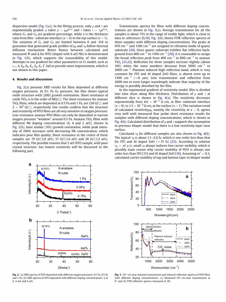
Transmission spectra for films with different doping concen-trations are shown in Fig. 3(a). Average transmission for all thesamples is about 75% in the range of visible light, which is close todata in references [6,19]. Fig. 3(b) shows FTIR reflective spectra ofthree samples with different doping concentrations. The peaks at470 cm�1 and 1100 cm�1 are assigned to vibration mode of quartzsubstrate [20]. Since quartz substrate exhibits flat reflective back-ground from 400 cm�1 to 1100 cm�1 [20], it is reasonable to assignthe broad reflection peak from 400 cm�1 to 800 cm�1 to anataseTiO2 [21,22]. Reflection for three samples increase slightly (about10%) when the wave numbers decrease from 5000 cm�1 to2000 cm�1. Plasmon induced high reflection band, which is verycommon for ITO and Al doped ZnO films, is absent even up to1300 cm�1 (w8 mm). Low transmission and reflection from2000 nm to even longer wavelength indicate that majority of theenergy is possibly absorbed by the film.
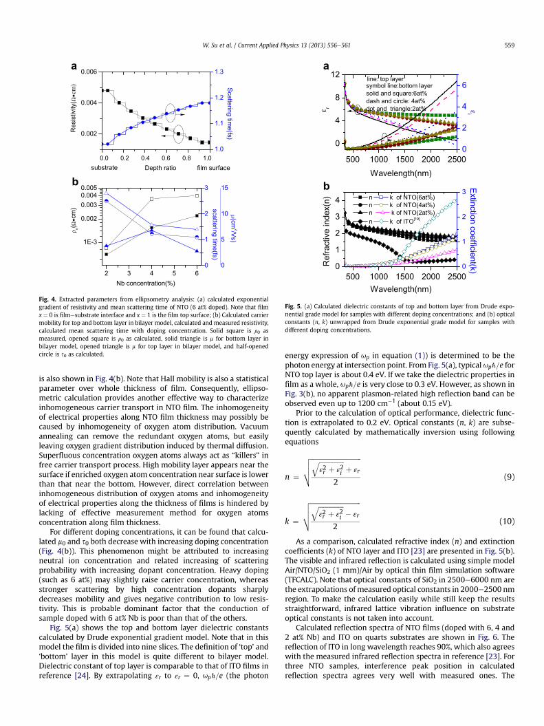
In the exponential gradient of resistivity model, film is dividedinto nine slices along film thickness. Distribution of r and s atdifferent slice is shown in Fig. 4(a). The resistivity decreasesexponentially from 4.6 � 10�3 U cm, at filmesubstrate interface(x¼ 0), to 1.3�10�3U cm, at the surface (x¼ 1). The variation trendof calculated resistivityr0, namely the resistivity at x ¼ 0, agreesvery well with measured four probe sheet resistance results forsamples with different doping concentrations, which is shown inFig. 4(b). Calculated distribution of r and s supports the assumptionin previous bilayer model that there is a low resistivity layer nearsurface.
Calculated s0 for different samples are also shown in Fig. 4(b).The typical s0 is about 1.1e2.6 fs, which is one order less than thatfor ITO and Al doped ZnO (w15 fs) [23]. According to relations0 ¼ m*m=e, small s0 always induces low carrier mobility, which ispossibly main reason why carrier mobility of NTO is always oneorder less than ITO [15] and Al doped ZnO [16]. Assumingm* ¼ 0.3,calculated carrier mobility of top and bottom layer in bilayer model
500 1000 1500 2000 25000
20
40
60
80
100
Tran
smis
sion
(%)
Wavelength(nm)
6at% 4at% 2at%
1000 2000 3000 4000 500020
40
60
80
100lattice vibration
induced reflection
Ref
lect
ion(
%)
Wavenumber (cm -1)
6at% 4at% 2at%CO2 noise
Plasmon inducedreflection
a
b
Fig. 3. UVevis-near infrared transmission and infrared reflection spectra of NTO filmswith different doping concentrations: (a) Measured UVevis-near transmission at0� and (b) FTIR reflective spectra measured at 30� .
0.0 0.2 0.4 0.6 0.8 1.0
0.002
0.004
0.006
film surfaceDepth ratio
Res
istiv
ity(
cm)
substrate
1.0
1.1
1.2
1.3
Scattering time(fs)
2 3 4 5 6
1E-3
0.002
0.0030.0040.005
(cm/Vs)
(cm
)
Nb concentration(%)
0
5
10
15
scattering time(fs)
0
1
2
3
a
b
Fig. 4. Extracted parameters from ellipsometry analysis: (a) calculated exponentialgradient of resistivity and mean scattering time of NTO (6 at% doped). Note that filmx ¼ 0 is filmesubstrate interface and x ¼ 1 is the film top surface; (b) Calculated carriermobility for top and bottom layer in bilayer model, calculated and measured resistivity,calculated mean scattering time with doping concentration. Solid square is r0 asmeasured, opened square is r0 as calculated, solid triangle is m for bottom layer inbilayer model, opened triangle is m for top layer in bilayer model, and half-openedcircle is s0 as calculated.
500 1000 1500 2000 2500
0
4
8
12
Wavelength(nm)
0
2
4
6line: top layersymbol line:bottom layersolid and square:6at%dash and circle: 4at%dot and triangle:2at%
500 1000 1500 2000 25000
1
2
3
4 n k of NTO(6at%) n k of NTO(4at%) n k of NTO(2at%) n k of ITO
Wavelength(nm)
Ref
ract
ive
inde
x(n)
0
1
2
3
Extinction coefficient(k)a
b
Fig. 5. (a) Calculated dielectric constants of top and bottom layer from Drude expo-nential grade model for samples with different doping concentrations; and (b) opticalconstants (n, k) unwrapped from Drude exponential grade model for samples withdifferent doping concentrations.
W. Su et al. / Current Applied Physics 13 (2013) 556e561 559
is also shown in Fig. 4(b). Note that Hall mobility is also a statisticalparameter over whole thickness of film. Consequently, ellipso-metric calculation provides another effective way to characterizeinhomogeneous carrier transport in NTO film. The inhomogeneityof electrical properties along NTO film thickness may possibly becaused by inhomogeneity of oxygen atom distribution. Vacuumannealing can remove the redundant oxygen atoms, but easilyleaving oxygen gradient distribution induced by thermal diffusion.Superfluous concentration oxygen atoms always act as “killers” infree carrier transport process. High mobility layer appears near thesurface if enriched oxygen atom concentration near surface is lowerthan that near the bottom. However, direct correlation betweeninhomogeneous distribution of oxygen atoms and inhomogeneityof electrical properties along the thickness of films is hindered bylacking of effective measurement method for oxygen atomsconcentration along film thickness.
For different doping concentrations, it can be found that calcu-lated m0 and s0 both decrease with increasing doping concentration(Fig. 4(b)). This phenomenon might be attributed to increasingneutral ion concentration and related increasing of scatteringprobability with increasing dopant concentration. Heavy doping(such as 6 at%) may slightly raise carrier concentration, whereasstronger scattering by high concentration dopants sharplydecreases mobility and gives negative contribution to low resis-tivity. This is probable dominant factor that the conduction ofsample doped with 6 at% Nb is poor than that of the others.
Fig. 5(a) shows the top and bottom layer dielectric constantscalculated by Drude exponential gradient model. Note that in thismodel the film is divided into nine slices. The definition of ‘top’ and‘bottom’ layer in this model is quite different to bilayer model.Dielectric constant of top layer is comparable to that of ITO films inreference [24]. By extrapolating εr to εr ¼ 0, upZ=e (the photon
energy expression of up in equation (1)) is determined to be thephoton energy at intersection point. From Fig. 5(a), typical upZ=e forNTO top layer is about 0.4 eV. If we take the dielectric properties infilm as a whole, upZ=e is very close to 0.3 eV. However, as shown inFig. 3(b), no apparent plasmon-related high reflection band can beobserved even up to 1200 cm�1 (about 0.15 eV).
Prior to the calculation of optical performance, dielectric func-tion is extrapolated to 0.2 eV. Optical constants (n, k) are subse-quently calculated by mathematically inversion using followingequations
n ¼
ffiffiffiffiffiffiffiffiffiffiffiffiffiffiffiffiffiffiffiffiffiffiffiffiffiffiffiffiffiffiffiffiffiffiffiffiffiffiffiffiffiffiffiffiffiε2r þ ε
2i
qþ εr
2
vuut(9)
k ¼
ffiffiffiffiffiffiffiffiffiffiffiffiffiffiffiffiffiffiffiffiffiffiffiffiffiffiffiffiffiffiffiffiffiffiffiffiffiffiffiffiffiffiffiffiffiε2r þ ε
2i
q� εr
2
vuut(10)
As a comparison, calculated refractive index (n) and extinctioncoefficients (k) of NTO layer and ITO [23] are presented in Fig. 5(b).The visible and infrared reflection is calculated using simple modelAir/NTO/SiO2 (1 mm)/Air by optical thin film simulation software(TFCALC). Note that optical constants of SiO2 in 2500e6000 nm arethe extrapolations of measured optical constants in 2000e2500 nmregion. To make the calculation easily while still keep the resultsstraightforward, infrared lattice vibration influence on substrateoptical constants is not taken into account.
Calculated reflection spectra of NTO films (doped with 6, 4 and2 at% Nb) and ITO on quarts substrates are shown in Fig. 6. Thereflection of ITO in long wavelength reaches 90%, which also agreeswith the measured infrared reflection spectra in reference [23]. Forthree NTO samples, interference peak position in calculatedreflection spectra agrees very well with measured ones. The
2000 4000 60000
20
40
60
80
100C
alcu
late
d re
flect
ion(
%)
Wavelength (nm)
6at% d=280nm 4at% d=262nm 2at% d=270nm ITO d=285nm
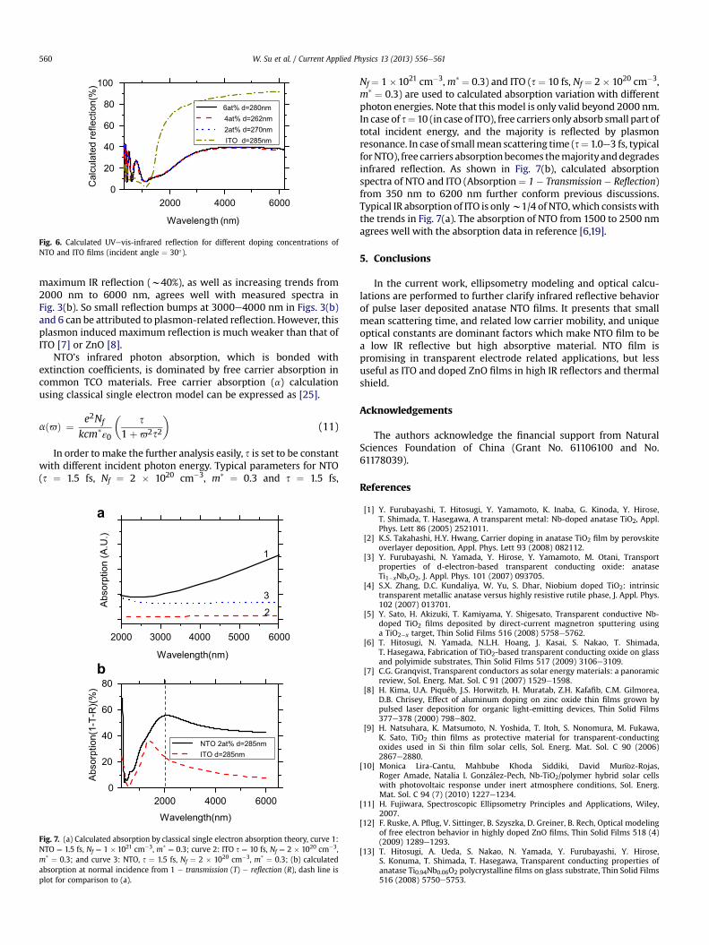
Fig. 6. Calculated UVevis-infrared reflection for different doping concentrations ofNTO and ITO films (incident angle ¼ 30�).
W. Su et al. / Current Applied Physics 13 (2013) 556e561560
maximum IR reflection (w40%), as well as increasing trends from2000 nm to 6000 nm, agrees well with measured spectra inFig. 3(b). So small reflection bumps at 3000e4000 nm in Figs. 3(b)and 6 can be attributed to plasmon-related reflection. However, thisplasmon induced maximum reflection is much weaker than that ofITO [7] or ZnO [8].
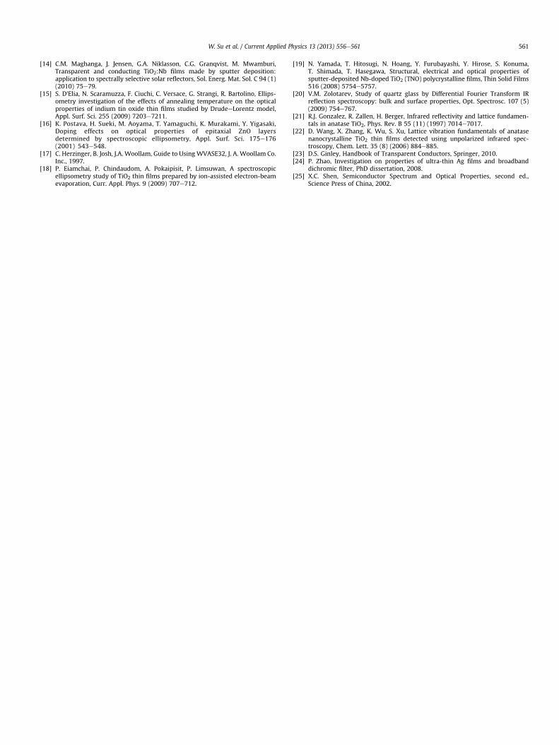
NTO’s infrared photon absorption, which is bonded withextinction coefficients, is dominated by free carrier absorption incommon TCO materials. Free carrier absorption (a) calculationusing classical single electron model can be expressed as [25].
að6Þ ¼ e2Nf
kcm*ε0
�s
1þ62s2
�(11)
In order to make the further analysis easily, s is set to be constantwith different incident photon energy. Typical parameters for NTO(s ¼ 1.5 fs, Nf ¼ 2 � 1020 cm�3, m* ¼ 0.3 and s ¼ 1.5 fs,
2000 3000 4000 5000 6000
Abso
rptio
n (A
.U.)
Wavelength(nm)
1
2
3
2000 4000 60000
20
40
60
80
Abso
rptio
n(1-
T-R
)(%)
Wavelength(nm)
NTO 2at% d=285nm ITO d=285nm
a
b
Fig. 7. (a) Calculated absorption by classical single electron absorption theory, curve 1:NTO ¼ 1.5 fs, Nf ¼ 1 � 1021 cm�3, m* ¼ 0.3; curve 2: ITO s ¼ 10 fs, Nf ¼ 2 � 1020 cm�3,m* ¼ 0.3; and curve 3: NTO, s ¼ 1.5 fs, Nf ¼ 2 � 1020 cm�3, m* ¼ 0.3; (b) calculatedabsorption at normal incidence from 1 � transmission (T) � reflection (R), dash line isplot for comparison to (a).
Nf ¼ 1 �1021 cm�3,m* ¼ 0.3) and ITO (s ¼ 10 fs, Nf ¼ 2 � 1020 cm�3,m* ¼ 0.3) are used to calculated absorption variation with differentphoton energies. Note that this model is only valid beyond 2000 nm.In case of s¼ 10 (in case of ITO), free carriers only absorb small part oftotal incident energy, and the majority is reflected by plasmonresonance. In case of smallmean scattering time (s¼ 1.0e3 fs, typicalforNTO), free carriers absorptionbecomes themajorityanddegradesinfrared reflection. As shown in Fig. 7(b), calculated absorptionspectra of NTO and ITO (Absorption¼ 1� Transmission� Reflection)from 350 nm to 6200 nm further conform previous discussions.Typical IR absorption of ITO is onlyw1/4 of NTO,which consistswiththe trends in Fig. 7(a). The absorption of NTO from 1500 to 2500 nmagrees well with the absorption data in reference [6,19].
5. Conclusions
In the current work, ellipsometry modeling and optical calcu-lations are performed to further clarify infrared reflective behaviorof pulse laser deposited anatase NTO films. It presents that smallmean scattering time, and related low carrier mobility, and uniqueoptical constants are dominant factors which make NTO film to bea low IR reflective but high absorptive material. NTO film ispromising in transparent electrode related applications, but lessuseful as ITO and doped ZnO films in high IR reflectors and thermalshield.
Acknowledgements
The authors acknowledge the financial support from NaturalSciences Foundation of China (Grant No. 61106100 and No.61178039).
References
[1] Y. Furubayashi, T. Hitosugi, Y. Yamamoto, K. Inaba, G. Kinoda, Y. Hirose,T. Shimada, T. Hasegawa, A transparent metal: Nb-doped anatase TiO2, Appl.Phys. Lett 86 (2005) 2521011.
[2] K.S. Takahashi, H.Y. Hwang, Carrier doping in anatase TiO2 film by perovskiteoverlayer deposition, Appl. Phys. Lett 93 (2008) 082112.
[3] Y. Furubayashi, N. Yamada, Y. Hirose, Y. Yamamoto, M. Otani, Transportproperties of d-electron-based transparent conducting oxide: anataseTi1�xNbxO2, J. Appl. Phys. 101 (2007) 093705.
[4] S.X. Zhang, D.C. Kundaliya, W. Yu, S. Dhar, Niobium doped TiO2: intrinsictransparent metallic anatase versus highly resistive rutile phase, J. Appl. Phys.102 (2007) 013701.
[5] Y. Sato, H. Akizuki, T. Kamiyama, Y. Shigesato, Transparent conductive Nb-doped TiO2 films deposited by direct-current magnetron sputtering usinga TiO2�x target, Thin Solid Films 516 (2008) 5758e5762.
[6] T. Hitosugi, N. Yamada, N.L.H. Hoang, J. Kasai, S. Nakao, T. Shimada,T. Hasegawa, Fabrication of TiO2-based transparent conducting oxide on glassand polyimide substrates, Thin Solid Films 517 (2009) 3106e3109.
[7] C.G. Granqvist, Transparent conductors as solar energy materials: a panoramicreview, Sol. Energ. Mat. Sol. C 91 (2007) 1529e1598.
[8] H. Kima, U.A. Piquéb, J.S. Horwitzb, H. Muratab, Z.H. Kafafib, C.M. Gilmorea,D.B. Chrisey, Effect of aluminum doping on zinc oxide thin films grown bypulsed laser deposition for organic light-emitting devices, Thin Solid Films377e378 (2000) 798e802.
[9] H. Natsuhara, K. Matsumoto, N. Yoshida, T. Itoh, S. Nonomura, M. Fukawa,K. Sato, TiO2 thin films as protective material for transparent-conductingoxides used in Si thin film solar cells, Sol. Energ. Mat. Sol. C 90 (2006)2867e2880.
[10] Monica Lira-Cantu, Mahbube Khoda Siddiki, David Muneoz-Rojas,Roger Amade, Natalia I. González-Pech, Nb-TiO2/polymer hybrid solar cellswith photovoltaic response under inert atmosphere conditions, Sol. Energ.Mat. Sol. C 94 (7) (2010) 1227e1234.
[11] H. Fujiwara, Spectroscopic Ellipsometry Principles and Applications, Wiley,2007.
[12] F. Ruske, A. Pflug, V. Sittinger, B. Szyszka, D. Greiner, B. Rech, Optical modelingof free electron behavior in highly doped ZnO films, Thin Solid Films 518 (4)(2009) 1289e1293.
[13] T. Hitosugi, A. Ueda, S. Nakao, N. Yamada, Y. Furubayashi, Y. Hirose,S. Konuma, T. Shimada, T. Hasegawa, Transparent conducting properties ofanatase Ti0.94Nb0.06O2 polycrystalline films on glass substrate, Thin Solid Films516 (2008) 5750e5753.
W. Su et al. / Current Applied Physics 13 (2013) 556e561 561
[14] C.M. Maghanga, J. Jensen, G.A. Niklasson, C.G. Granqvist, M. Mwamburi,Transparent and conducting TiO2:Nb films made by sputter deposition:application to spectrally selective solar reflectors, Sol. Energ. Mat. Sol. C 94 (1)(2010) 75e79.
[15] S. D’Elia, N. Scaramuzza, F. Ciuchi, C. Versace, G. Strangi, R. Bartolino, Ellips-ometry investigation of the effects of annealing temperature on the opticalproperties of indium tin oxide thin films studied by DrudeeLorentz model,Appl. Surf. Sci. 255 (2009) 7203e7211.
[16] K. Postava, H. Sueki, M. Aoyama, T. Yamaguchi, K. Murakami, Y. Yigasaki,Doping effects on optical properties of epitaxial ZnO layersdetermined by spectroscopic ellipsometry, Appl. Surf. Sci. 175e176(2001) 543e548.
[17] C. Herzinger, B. Josh, J.A. Woollam, Guide to Using WVASE32, J. A. Woollam Co.Inc., 1997.
[18] P. Eiamchai, P. Chindaudom, A. Pokaipisit, P. Limsuwan, A spectroscopicellipsometry study of TiO2 thin films prepared by ion-assisted electron-beamevaporation, Curr. Appl. Phys. 9 (2009) 707e712.
[19] N. Yamada, T. Hitosugi, N. Hoang, Y. Furubayashi, Y. Hirose, S. Konuma,T. Shimada, T. Hasegawa, Structural, electrical and optical properties ofsputter-deposited Nb-doped TiO2 (TNO) polycrystalline films, Thin Solid Films516 (2008) 5754e5757.
[20] V.M. Zolotarev, Study of quartz glass by Differential Fourier Transform IRreflection spectroscopy: bulk and surface properties, Opt. Spectrosc. 107 (5)(2009) 754e767.
[21] R.J. Gonzalez, R. Zallen, H. Berger, Infrared reflectivity and lattice fundamen-tals in anatase TiO2, Phys. Rev. B 55 (11) (1997) 7014e7017.
[22] D. Wang, X. Zhang, K. Wu, S. Xu, Lattice vibration fundamentals of anatasenanocrystalline TiO2 thin films detected using unpolarized infrared spec-troscopy, Chem. Lett. 35 (8) (2006) 884e885.
[23] D.S. Ginley, Handbook of Transparent Conductors, Springer, 2010.[24] P. Zhao, Investigation on properties of ultra-thin Ag films and broadband
dichromic filter, PhD dissertation, 2008.[25] X.C. Shen, Semiconductor Spectrum and Optical Properties, second ed.,
Science Press of China, 2002.