![7. Heteroscedasticitylipas.uwasa.fi/~bepa/ecmc7.pdf · 2012-10-01 · 7.1 Consequences In the presence of heteroscedasticity: (i) OLS estimators are not BLUE (ii) Var[ ^ j]are biased,](https://static.fdocument.org/doc/165x107/5f77fc3d0b125015ba6f2530/7-het-bepaecmc7pdf-2012-10-01-71-consequences-in-the-presence-of-heteroscedasticity.jpg)
ALPA MGA A0651202 SEMICONDUCTOR · JS (Max) =175˚C TC = 25˚C Figure 17. Maximum Forward Biased...
9
AOK065V120X2 1200V αSiC Silicon Carbide Power MOSFET Rev. 1.0 March 2020 www.aosmd.com Page 1 of 9 ALPHA & OMEGA SEMICONDUCTOR Features • Proprietary αSiC MOSFET technology • Low loss, fast switching speeds with low RG • Optimized drive voltage (VGS =15V) for broad driver compatibility • Robust body diode and low Qrr Applications • Renewable • Industrial • EV Charger • UPS • Solar Inverters • SMPS • Motor Drives Product Summary VDS @ TJ, max 1200V IDM 85A RDS(ON), typ 65mΩ Qrr 164nC EOSS @ 800V 36µJ 100% UIS Tested Ordering Part Number Package Type Form Shipping Quantity AOK065V120X2 TO-247-3L Tube 30/Tube Absolute Maximum Ratings (TA = 25°C, unless otherwise noted) Symbol Parameter AOK065V120X2 Units V DS Drain-Source Voltage 1200 V V GS, MAX Gate-Source Voltage Maximum -8/+18 V V GS,OP,TRANS Max Transient (A) -8/+20 V GS,OP Recommended Operating (B) -5/+15 I D Continuous Drain Current TC = 25°C 40.3 A TC = 100°C 29.6 I DM Pulsed Drain Current (C) 85 E AS Single Pulsed Avalanche Energy (D) 250 mJ P D Power Dissipation (C) 187.5 W T J, TSTG Junction and Storage Temperature Range -55 to 175 °C T L Maximum lead temperature for soldering purpose, 1/8” from case for 5 seconds 300 °C Pin Configuration Top View (1) (2) (3) Bottom View G (1) S (3) D (2)
Transcript of ALPA MGA A0651202 SEMICONDUCTOR · JS (Max) =175˚C TC = 25˚C Figure 17. Maximum Forward Biased...

AOK065V120X21200V αSiC Silicon Carbide
Power MOSFET
Rev. 1.0 March 2020 www.aosmd.com Page 1 of 9
ALPHA & OMEGAS EM ICONDUCTOR
Features• Proprietary αSiC MOSFET technology• Low loss, fast switching speeds with low RG • Optimized drive voltage (VGS =15V)
for broad driver compatibility• Robust body diode and low Qrr
Applications• Renewable • Industrial• EV Charger • UPS• Solar Inverters • SMPS
• Motor Drives
Product SummaryVDS @ TJ, max 1200VIDM 85ARDS(ON), typ 65mΩQrr 164nCEOSS @ 800V 36µJ100% UIS Tested
Ordering Part Number Package Type Form Shipping QuantityAOK065V120X2 TO-247-3L Tube 30/Tube
Absolute Maximum Ratings (TA = 25°C, unless otherwise noted)
Symbol Parameter AOK065V120X2 UnitsVDS Drain-Source Voltage 1200 V
VGS, MAX
Gate-Source Voltage
Maximum -8/+18
VVGS,OP,TRANS Max Transient(A) -8/+20VGS,OP Recommended Operating (B) -5/+15
ID Continuous Drain CurrentTC = 25°C 40.3
ATC = 100°C 29.6IDM Pulsed Drain Current(C) 85 EAS Single Pulsed Avalanche Energy(D) 250 mJPD Power Dissipation(C) 187.5 W
TJ, TSTG Junction and Storage Temperature Range -55 to 175 °CTL Maximum lead temperature for soldering purpose, 1/8” from case for 5 seconds 300 °C
Pin Configuration
Top View
(1)(2)
(3)
Bottom View
G
D
S
G(1)
S(3)
D(2)
Rev. 1.0 March 2020 www.aosmd.com Page 2 of 9
AOK065V120X2ALPHA & OMEGAS EM ICONDUCTOR
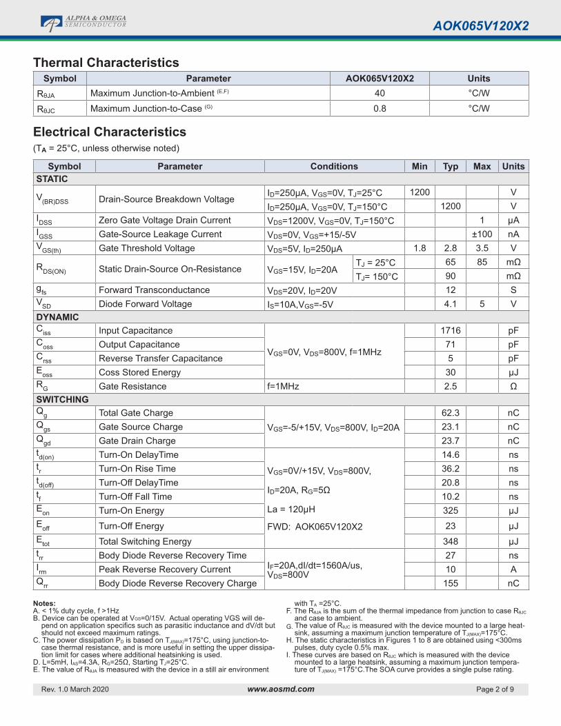
Thermal CharacteristicsSymbol Parameter AOK065V120X2 Units
RθJA Maximum Junction-to-Ambient (E,F) 40 °C/W
RθJC Maximum Junction-to-Case (G) 0.8 °C/W
Electrical Characteristics(TA = 25°C, unless otherwise noted)
Symbol Parameter Conditions Min Typ Max UnitsSTATIC
V(BR)DSS Drain-Source Breakdown VoltageID=250µA, VGS=0V, TJ=25°C 1200 VID=250µA, VGS=0V, TJ=150°C 1200 V
IDSS Zero Gate Voltage Drain Current VDS=1200V, VGS=0V, TJ=150°C 1 µAIGSS Gate-Source Leakage Current VDS=0V, VGS=+15/-5V ±100 nAVGS(th) Gate Threshold Voltage VDS=5V, ID=250µA 1.8 2.8 3.5 V
RDS(ON) Static Drain-Source On-Resistance VGS=15V, ID=20ATJ = 25°C 65 85 mΩTJ= 150°C 90 mΩ
gfs Forward Transconductance VDS=20V, ID=20V 12 SVSD Diode Forward Voltage IS=10A,VGS=-5V 4.1 5 VDYNAMIC Ciss Input Capacitance
VGS=0V, VDS=800V, f=1MHz
1716 pFCoss Output Capacitance 71 pFCrss Reverse Transfer Capacitance 5 pFEoss Coss Stored Energy 30 µJRG Gate Resistance f=1MHz 2.5 ΩSWITCHING Qg Total Gate Charge
VGS=-5/+15V, VDS=800V, ID=20A62.3 nC
Qgs Gate Source Charge 23.1 nCQgd Gate Drain Charge 23.7 nCtd(on) Turn-On DelayTime
VGS=0V/+15V, VDS=800V,
ID=20A, RG=5Ω
La = 120µH
FWD: AOK065V120X2
14.6 nstr Turn-On Rise Time 36.2 nstd(off) Turn-Off DelayTime 20.8 nstf Turn-Off Fall Time 10.2 nsEon Turn-On Energy 325 µJEoff Turn-Off Energy 23 µJEtot Total Switching Energy 348 µJtrr Body Diode Reverse Recovery Time
IF=20A,dI/dt=1560A/us, VDS=800V
27 nsIrm Peak Reverse Recovery Current 10 AQrr Body Diode Reverse Recovery Charge 155 nC
Notes:A. < 1% duty cycle, f >1HzB. Device can be operated at VGS=0/15V. Actual operating VGS will de-
pend on application specifics such as parasitic inductance and dV/dt but should not exceed maximum ratings.
C. The power dissipation PD is based on TJ(MAX)=175°C, using junction-to-case thermal resistance, and is more useful in setting the upper dissipa-tion limit for cases where additional heatsinking is used.
D. L=5mH, IAS=4.3A, RG=25Ω, Starting TJ=25°C.E. The value of RθJA is measured with the device in a still air environment
with TA =25°C. F. The RθJA is the sum of the thermal impedance from junction to case RθJC
and case to ambient.G. The value of RθJC is measured with the device mounted to a large heat-
sink, assuming a maximum junction temperature of TJ(MAX)=175°C.H. The static characteristics in Figures 1 to 8 are obtained using <300ms
pulses, duty cycle 0.5% max.I. These curves are based on RθJC which is measured with the device
mounted to a large heatsink, assuming a maximum junction tempera-ture of TJ(MAX) =175°C.The SOA curve provides a single pulse rating.
Rev. 1.0 March 2020 www.aosmd.com Page 3 of 9
AOK065V120X2ALPHA & OMEGAS EM ICONDUCTOR
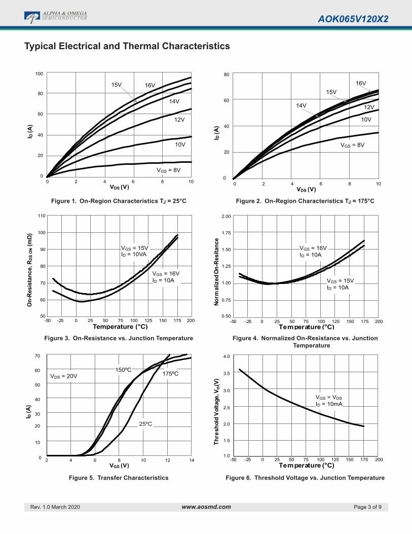
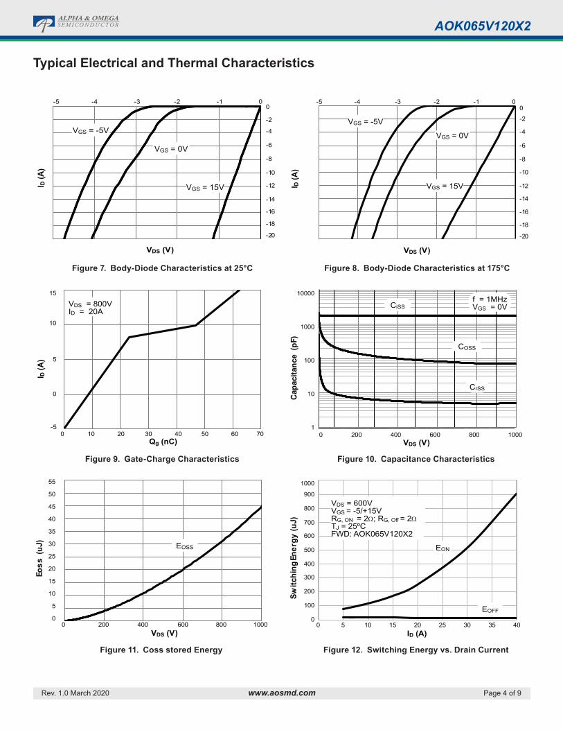
Typical Electrical and Thermal Characteristics
0
20
40
60
80
100
I D (A
)
VDS (V)6 8 102 40
15V
16V
14V
12V
10V
VGS = 8V
Figure 1. On-Region Characteristics TJ = 25°C
0
20
40
60
80
2 4 6 8VDS (V)
I D (A
)
0 10
15V
16V
14V
12V
10V
VGS = 8V
Figure 2. On-Region Characteristics TJ = 175°C
Temperature (°C)
On-
Resi
stan
ce, R
DS O
N (m
Ω)
50
60
70
80
90
100
110
-50 -25 0 25 50 75 100 125 150 175 200
VGS = 15VID = 10VA
VGS = 16VID = 10A
Figure 3. On-Resistance vs. Junction Temperature
Temperature (°C)0.50
0.75
1.00
1.25
1.50
1.75
2.00
-50 -25 0 25 50 75 100 125 150 175 200
Norm
aliz
ed O
n-Re
sita
nce
-
VGS = 16VID = 10A
VGS = 15VID = 10A
Figure 4. Normalized On-Resistance vs. Junction Temperature
VGS (V)0
10
20
30
40
50
60
70
2 4 6 8 10 12 14
I D (A
)
VDS = 20V
150ºC
175ºC
25ºC
Figure 5. Transfer Characteristics
1.0
1.5
2.0
2.5
3.0
3.5
4.0
Thre
shol
d Vo
ltage
, Vth
(V)
Temperature (°C)-50 -25 0 25 50 75 100 125 150 175 200
VGS = VDSID = 10mA
Figure 6. Threshold Voltage vs. Junction Temperature
Rev. 1.0 March 2020 www.aosmd.com Page 4 of 9
AOK065V120X2ALPHA & OMEGAS EM ICONDUCTOR
Typical Electrical and Thermal Characteristics
-20
-18
-16
-14
-12
-10
-8
-6
-4
-2
0-5 -4 -3 -2 -1 0
I D (A
)
VDS (V)
VGS = -5V
VGS = 0V
VGS = 15V
Figure 7. Body-Diode Characteristics at 25°C
-20
-18
-16
-14
-12
-10
-8
-6
-4
-2
0
I D (A
)
VDS (V)
VGS = -5V
VGS = 0V
VGS = 15V
-5 -4 -3 -2 -1 0
Figure 8. Body-Diode Characteristics at 175°C
-5
0
5
10
15
0 10 20 30 40 50 60 70
I D (A
)
Qg (nC)
VDS = 800VID = 20A
Figure 9. Gate-Charge Characteristics
1
10
100
1000
10000
0 200 400 600 800 1000
Capa
cita
nce
(pF)
VDS (V)
CiSS
COSS
CrSS
f = 1MHzVGS = 0V
Figure 10. Capacitance Characteristics
0
5
10
15
20
25
30
35
40
45
50
55
0 200 400 600 800 1000
Eoss
(uJ
)
VDS (V)
EOSS
Figure 11. Coss stored Energy
0
100
200
300
400
500
600
700
800
900
1000
0 5 10 15 20 25 30 35 40
Switc
hing
Ener
gy (
uJ)
ID (A)
EON
EOFF
VDS = 600VVGS = -5/+15VRG, ON = 2Ω; RG, Off = 2ΩTJ = 25ºCFWD: AOK065V120X2
Figure 12. Switching Energy vs. Drain Current
Rev. 1.0 March 2020 www.aosmd.com Page 5 of 9
AOK065V120X2ALPHA & OMEGAS EM ICONDUCTOR
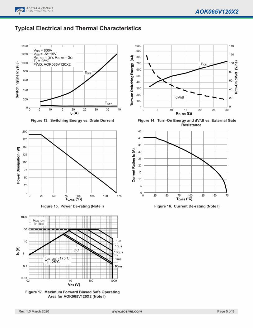
Typical Electrical and Thermal Characteristics
VDS = 800VVGS = -5/+15VRG, ON = 2Ω; RG, Off = 2ΩTJ = 25ºCFWD: AOK065V120X2
EON
EOFF0
200
400
600
800
1000
1200
1400
0 5 10 15 20 25 30 35 40
Switc
hing
Ener
gy (u
J)
ID (A)
Figure 13. Switching Energy vs. Drain Durrent
EON
dV/dt
0
20
40
60
80
100
120
140
0
100
200
300
400
500
600
700
800
900
1000
0 5 10 15 20 25 30
Tutn
-On
dV/d
t (V
/ns)
Turn
-on
Switc
hing
Ener
gy (
uJ)
RG, ON (Ω)
Figure 14. Turn-On Energy and dV/dt vs. External Gate Resistance
Pow
er D
issi
patio
n (W
)
0
25
50
75
100
125
150
175
200
0 25 50 75 100 125 150 175TCASE (°C)
Figure 15. Power De-rating (Note I)
Cur
rent
Rat
ing
I D (A
)
0 25 50 75 100 125 150 175TCASE (°C)
0
5
10
15
20
25
30
35
40
45
Figure 16. Current De-rating (Note I)
°
RDS (ON)limited
10µs
1µs
100µs
10ms
1ms
DC
VDS (V)
0.01
0.1
1
10
100
1000
0.1 1 10 100 1000
I D (A
)
TJS (Max) =175˚CTC = 25˚C
Figure 17. Maximum Forward Biased Safe Operating Area for AOK065V120X2 (Note I)
Rev. 1.0 March 2020 www.aosmd.com Page 6 of 9
AOK065V120X2ALPHA & OMEGAS EM ICONDUCTOR
Typical Electrical and Thermal Characteristics
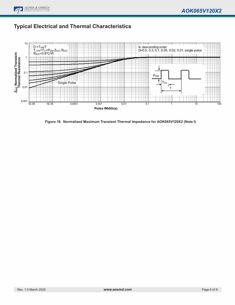
0.001
0.01
0.1
1
10
1E-06 1E-05 0.0001 0.001 0.01 0.1 1 10 100
Z θJC
Nor
mal
ized
Tra
nsie
nt
Ther
mal
Res
ista
nce
Pulse Width(s)
T
D =TON/TTJ,PK=TC+PDM.ZθJC.RθJCRθJC=0.8ºC/W
In descending orderD=0.5, 0.3, 0.1, 0.05, 0.02, 0.01, single pulse
Single Pulse
PDM
TOn
Figure 18. Normalized Maximum Transient Thermal Impedance for AOK065V120X2 (Note I)

Rev. 1.0 March 2020 www.aosmd.com Page 7 of 9
AOK065V120X2ALPHA & OMEGAS EM ICONDUCTOR
-+
VDC
Ig
Vds
DUT-+
VDC
Vgs
Vgs
10V
Qg
Qgs Qgd
Charge
Gate Charge Test Circuit & Waveform
-+
VDCDUT VddVgs
Vds
Vgs
RL
Rg
Vgs
Vds
10%
90%
Resistive Switching Test Circuit & Waveforms
t trd(on)
ton
td(off) tf
toff
VddVgs
Id
Vgs
Rg
DUT
-+
VDC
L
Vgs
Vds
Id
Vgs
BV
I
Unclamped Inductive Switching (UIS) Test Circuit & Waveforms
Ig
Vgs-+
VDC
DUT
L
Vds
Vgs
Vds
IsdIsd
Diode Recovery Test Circuit & Waveforms
Vds -
Vds +
IF
AR
DSS
2E = 1/2 LI
dI/dtIRM
rr
VddVdd
Q = - Idt
ARAR
trr
Test Circuits and Waveforms
Gate Charge Test Circuits and Waveforms
Resistive Switching Test Circuit and Waveforms
Unclamped Inductive Switching (UIS) Test Circuit and Waveforms
Gate Charge Test Circuits and Waveforms
Rev. 1.0 March 2020 www.aosmd.com Page 8 of 9
AOK065V120X2ALPHA & OMEGAS EM ICONDUCTOR
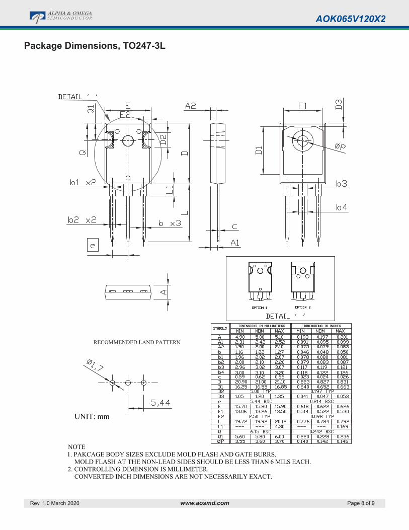
RECOMMENDED LAND PATTERN
UNIT: mm
NOTE1. PAKCAGE BODY SIZES EXCLUDE MOLD FLASH AND GATE BURRS. MOLD FLASH AT THE NON-LEAD SIDES SHOULD BE LESS THAN 6 MILS EACH.2. CONTROLLING DIMENSION IS MILLIMETER. CONVERTED INCH DIMENSIONS ARE NOT NECESSARILY EXACT.
Package Dimensions, TO247-3L
Rev. 1.0 March 2020 www.aosmd.com Page 9 of 9
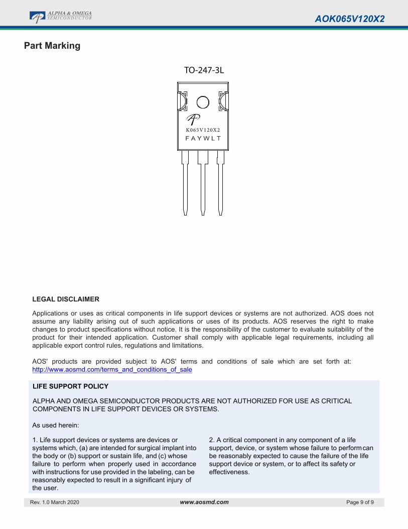
AOK065V120X2ALPHA & OMEGAS EM ICONDUCTOR
Part Marking
K065V120X2
TO-247-3L
LEGAL DISCLAIMER
Applications or uses as critical components in life support devices or systems are not authorized. AOS does not assume any liability arising out of such applications or uses of its products. AOS reserves the right to make changes to product specifications without notice. It is the responsibility of the customer to evaluate suitability of the product for their intended application. Customer shall comply with applicable legal requirements, including all applicable export control rules, regulations and limitations.
AOS' products are provided subject to AOS' terms and conditions of sale which are set forth at: http://www.aosmd.com/terms_and_conditions_of_sale
LIFE SUPPORT POLICY
ALPHA AND OMEGA SEMICONDUCTOR PRODUCTS ARE NOT AUTHORIZED FOR USE AS CRITICAL COMPONENTS IN LIFE SUPPORT DEVICES OR SYSTEMS.
As used herein:
1. Life support devices or systems are devices or 2. A critical component in any component of a lifesystems which, (a) are intended for surgical implant into support, device, or system whose failure to perform can the body or (b) support or sustain life, and (c) whose be reasonably expected to cause the failure of the life failure to perform when properly used in accordance support device or system, or to affect its safety or with instructions for use provided in the labeling, can be effectiveness. reasonably expected to result in a significant injury of the user.


![SELF-SHRINKERS TO THE MEAN CURVATURE FLOW …js/isoparametric.shrinker.final.pdf · This is a seemingly ill-posed problem since by the uniqueness theorem of Lu Wang [21], we cannot](https://static.fdocument.org/doc/165x107/60fb01b2d1ad03084b7f1a93/self-shrinkers-to-the-mean-curvature-flow-js-this-is-a-seemingly-ill-posed-problem.jpg)