
Additive manufacturing of 3D nano-architected metals nano-architectures were then pyrolyzed to...
8
ARTICLE Additive manufacturing of 3D nano-architected metals Andrey Vyatskikh 1 , Stéphane Delalande 2 , Akira Kudo 1 , Xuan Zhang 3 , Carlos M. Portela 1 & Julia R. Greer 1 Most existing methods for additive manufacturing (AM) of metals are inherently limited to ~20–50 μm resolution, which makes them untenable for generating complex 3D-printed metallic structures with smaller features. We developed a lithography-based process to create complex 3D nano-architected metals with ~100 nm resolution. We first synthesize hybrid organic–inorganic materials that contain Ni clusters to produce a metal-rich photo- resist, then use two-photon lithography to sculpt 3D polymer scaffolds, and pyrolyze them to volatilize the organics, which produces a >90 wt% Ni-containing architecture. We demon- strate nanolattices with octet geometries, 2 μm unit cells and 300–400-nm diameter beams made of 20-nm grained nanocrystalline, nanoporous Ni. Nanomechanical experiments reveal their specific strength to be 2.1–7.2 MPa g -1 cm 3 , which is comparable to lattice architectures fabricated using existing metal AM processes. This work demonstrates an efficient pathway to 3D-print micro-architected and nano-architected metals with sub-micron resolution. DOI: 10.1038/s41467-018-03071-9 OPEN 1 Division of Engineering and Applied Sciences, California Institute of Technology, 1200 E. California Blvd., Pasadena, CA 91125, USA. 2 Scientific Department, PSA Group, Centre Technique de Vélizy 2, route de Gizy, Vélizy-Villacoublay 78943, France. 3 Center of Advanced Mechanics and Materials, Department of Engineering Mechanics, Tsinghua University, Beijing 10084, China. Correspondence and requests for materials should be addressed to J.R.G. (email: [email protected]) NATURE COMMUNICATIONS | (2018)9:593 | DOI: 10.1038/s41467-018-03071-9 | www.nature.com/naturecommunications 1 1234567890():,;
Transcript of Additive manufacturing of 3D nano-architected metals nano-architectures were then pyrolyzed to...
ARTICLE
Additive manufacturing of 3D nano-architectedmetalsAndrey Vyatskikh 1, Stéphane Delalande2, Akira Kudo1, Xuan Zhang3, Carlos M. Portela1 & Julia R. Greer1
Most existing methods for additive manufacturing (AM) of metals are inherently limited to
~20–50 μm resolution, which makes them untenable for generating complex 3D-printed
metallic structures with smaller features. We developed a lithography-based process to
create complex 3D nano-architected metals with ~100 nm resolution. We first synthesize
hybrid organic–inorganic materials that contain Ni clusters to produce a metal-rich photo-
resist, then use two-photon lithography to sculpt 3D polymer scaffolds, and pyrolyze them to
volatilize the organics, which produces a >90 wt% Ni-containing architecture. We demon-
strate nanolattices with octet geometries, 2 μm unit cells and 300–400-nm diameter beams
made of 20-nm grained nanocrystalline, nanoporous Ni. Nanomechanical experiments reveal
their specific strength to be 2.1–7.2MPa g−1 cm3, which is comparable to lattice architectures
fabricated using existing metal AM processes. This work demonstrates an efficient pathway
to 3D-print micro-architected and nano-architected metals with sub-micron resolution.
DOI: 10.1038/s41467-018-03071-9 OPEN
1 Division of Engineering and Applied Sciences, California Institute of Technology, 1200 E. California Blvd., Pasadena, CA 91125, USA. 2 Scientific Department,PSA Group, Centre Technique de Vélizy 2, route de Gizy, Vélizy-Villacoublay 78943, France. 3 Center of Advanced Mechanics and Materials, Department ofEngineering Mechanics, Tsinghua University, Beijing 10084, China. Correspondence and requests for materials should be addressed toJ.R.G. (email: [email protected])
NATURE COMMUNICATIONS | (2018) 9:593 |DOI: 10.1038/s41467-018-03071-9 |www.nature.com/naturecommunications 1
1234
5678
90():,;
Additive manufacturing (AM) represents a set of processesthat enable layer by layer fabrication of complex 3Dstructures using a wide range of materials that include
ceramics1, polymers2, and metals3. The development of metalAM has revolutionized the production of complex parts foraerospace, automotive and medical applications4,5. Today’sresolution of most commercially available metal AM processes is~20–50 μm6; no established method is available for printing 3Dfeatures below these dimensions7. It has been shown that uniquephenomena arise in metals with micro-dimensions and nano-dimensions, for example light trapping in optical meta-materials8
and enhanced mechanical resilience9–15. Accessing thesephenomena requires developing a process to fabricate 3D metallicarchitectures with macroscopic overall dimensions and individualconstituents in the sub-micron regime.
Minimum feature size in metal AM is generally limited by thematerial feedstock, i.e., the method of supplying metal in powder,wire, sheet or ink form during fabrication. Inkjet-basedmethods16,17 manipulate 40–60 μm droplets of metal inks,limiting the smallest features to at least the size of a solidifieddroplet. Wire-based and filament-based processes, such as plasmadeposition4 and electron beam freeform fabrication (EBF3)18, relyon locally melting a >100 μm-diameter metal wire, which pro-duces millimeter-sized features. Powder-based processes, such asselective laser melting (SLM) and laser engineered net shaping19,consolidate ~0.3–10 μm metal powder particles, which limits thesmallest feature size to about 20 μm6,20. Overcoming these reso-lution limitations requires a capability to manipulate nanoscalequantities of metals in a stable and scalable 3D printing process.
Alternative material feeds to fabricate 3D metal structures with<10 μm resolution include nanoparticle inks, ion solutions, dro-plets of molten metal, and precursor gases7. Methods that uselocalized electroplating21,22 or metal ion reduction23,24 arecapable of producing features down to 500 nm using a very slowprocess that is limited by electroplating rate. Electrochemicalfabrication (EFAB) allows for manufacturing geometries with10-μm features and 4-μm layers, but is limited to structures with atotal height of 25–50 layers25. Other technologies, like micro-deposition of metal nanoparticle inks26–28 or molten metal29 andfocused ion beam direct writing, also suffer from slow throughputand are more suited for low-volume fabrication and repair30.
We demonstrate a facile and reproducible process to createcomplex 3D metal geometries with a resolution of 25–100-nm.We synthesize hybrid organic–inorganic materials that contain Niclusters and use them to produce a metal-rich photoresist. Wethen use two-photon lithography (TPL) to sculpt computer-designed architectures out of the resist and pyrolyze them first ininert atmosphere at 1000 °C and then in reducing atmosphere at600 °C to volatilize the organic constituents. Using this approach,we demonstrate the fabrication of periodic Ni octet nanolatticeswith the unit cell size of 2 μm and beam diameters of 300–400 nmdiameter as a proof-of-concept. TEM analysis reveals that themicrostructure of Ni beams is nanocrystalline and nanoporous,with a 20 nm mean grain size and 10–30% porosity within eachbeam. Nanomechanical experiments demonstrate that thestrength of these Ni nanolattices is comparable to that of themetal lattices with 0.1–1.0 mm beam diameters fabricated usingalternative metal AM technologies. These findings suggest anefficient pathway to create complex 3D metal structures withnano-scale resolution.
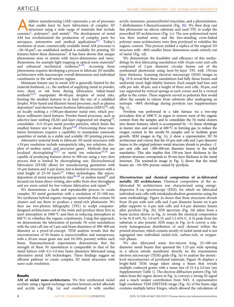
ResultsAM of nickel nano-architectures. We first synthesized nickelacrylate using a ligand exchange reaction between nickel alkoxideand acrylic acid (Fig. 1a) and combined it with another
acrylic monomer, pentaerythritol triacrylate, and a photoinitiator,7-diethylamino-3-thenoylcoumarin (Fig. 1b). We then drop castthis photoresist on silicon substrate and used TPL to sculpt theprescribed 3D architectures (Fig. 1c). The non-polymerized resistwas then washed away, and the free-standing cross-linkedpolymer nano-architectures were then pyrolyzed to volatilize theorganic content. This process yielded a replica of the original 3Dstructure with ~80% smaller linear dimensions made entirely outof metal (Fig. 1d).
We demonstrate the feasibility and efficiency of this metho-dology by first fabricating nanolattices with 10 μm octet unit cellscomprised of 2-μm diameter circular beams out of thesynthesized photoresist using layer-by-layer TPL with 150 nmlayer thickness. Scanning electron microscopy (SEM) images inFig. 1f–h reveal that these nanolattices had fully dense beams anduniformly sized, high-fidelity features. Each sample had four unitcells per side, 40 μm, and a height of three unit cells, 30 μm, andwas supported by vertical springs at each corner and by a verticalpillar in the center. These supports served as pedestals that wouldallow the sample to release from substrate after undergoing anisotropic ~80% shrinkage during pyrolysis (see SupplementaryFig. 1).
Pyrolysis was performed in a tube furnace via a two-stepprocedure: first at 1000 °C in argon to remove most of the organiccontent from the samples and to consolidate the Ni metal clustersinto denser features, which is accompanied by ~5× linear shrinkagein feature size; and second at 600 °C in forming gas, to reduce theoxygen content in the mostly-Ni samples and to facilitate graingrowth. SEM images in Fig. 1(i, j) show a representative 3D Niarchitecture and convey that the 10-μm unit cells and 2-μm diameterbeams in the original polymer-metal structure shrank to produce ~2μm unit cells and ~300–400 nm diameter beams in the nickelnanolattice. This also implies that 150-nm layer thickness in thepolymer structure corresponds to 30-nm layer thickness in the metalstructure. The zoomed-in image in Fig. 1j shows that the metalbeams are ~10–30% porous caused by pyrolysis.
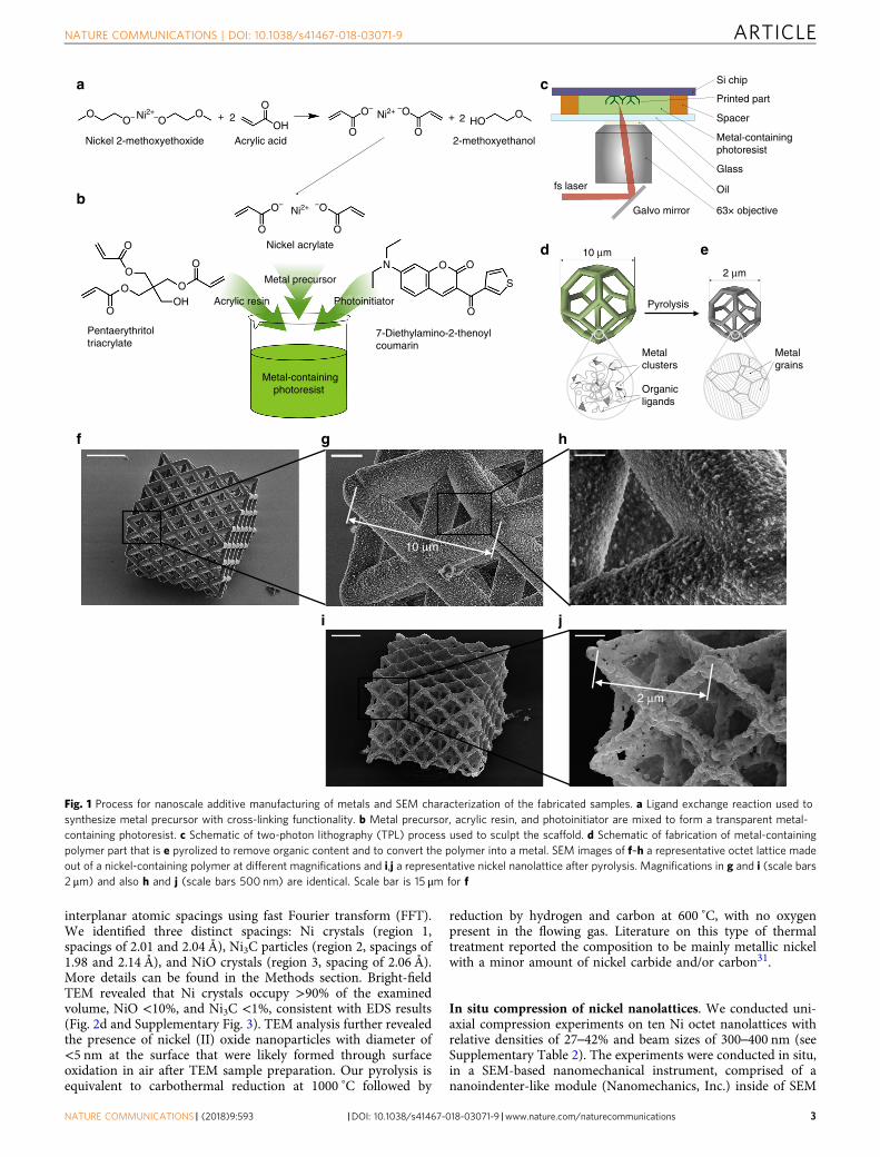
Microstructure and chemical composition of as-fabricatedmetallic 3D architectures. Chemical composition of the as-fabricated Ni architectures was characterized using energy-dispersive X-ray spectroscopy (EDS), for which we fabricatedindividual unit cells with tetrakaidecahedron geometries using thesame methodology. Figure 2a shows that these structures shrunkfrom 20-μm wide unit cells and 2-μm diameter beams on 6-μmpillar supports to 4-μm unit cells and 0.4-μm diameter beamsafter pyrolysis (Fig. 2b). EDS spectrum (Fig. 2d) taken from abeam section shown in Fig. 2c reveals the chemical compositionto be 91.8 wt% Ni, 5.0 wt% O, and 3.2 wt% C. A Si peak from thesubstrate is also present. EDS maps in Fig. 2e–h convey a rela-tively homogeneous distribution of each element within theprinted structure, which consists mostly of nickel metal and is notsegregated into individual nickel-rich, carbon-rich, or oxygen-rich phases.
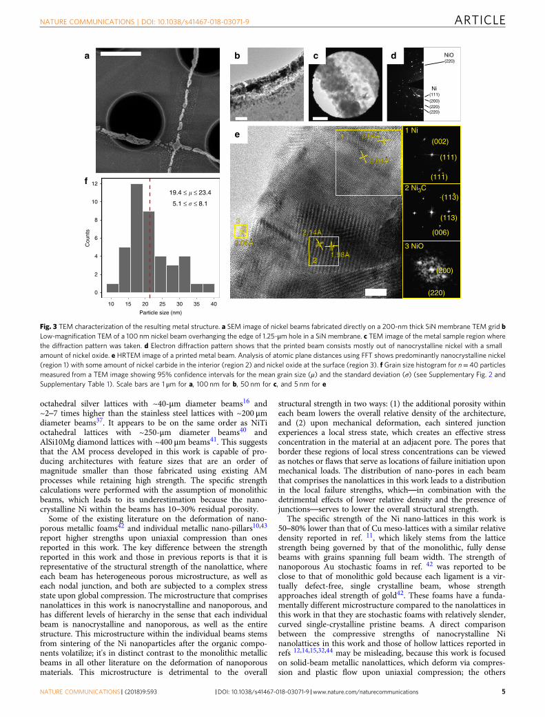
We also fabricated some few-micron long, 25–100-nmdiameter metal beams that spanned the 1.25-μm wide openingin a silicon nitride membrane directly on the transmissionelectron microscopy (TEM) grids (Fig. 3a) to analyze the atomic-level microstructure of pyrolyzed materials. Figure 3b displays abright-field TEM image taken along a beam that revealsmultiple coalesced grains with a mean size of 21.4± 2.0 nm (seeSupplementary Table 1). The electron diffraction pattern (Fig. 3d)taken from the region shown in Fig. 3c conveys a strong Ni signaland a much weaker contribution from NiO. A representativehigh-resolution TEM (HRTEM) image (Fig. 3e) of the beam edgecontains multiple lattice fringes, which allowed the calculation of
ARTICLE NATURE COMMUNICATIONS | DOI: 10.1038/s41467-018-03071-9
2 NATURE COMMUNICATIONS | (2018) 9:593 |DOI: 10.1038/s41467-018-03071-9 |www.nature.com/naturecommunications
interplanar atomic spacings using fast Fourier transform (FFT).We identified three distinct spacings: Ni crystals (region 1,spacings of 2.01 and 2.04 Å), Ni3C particles (region 2, spacings of1.98 and 2.14 Å), and NiO crystals (region 3, spacing of 2.06 Å).More details can be found in the Methods section. Bright-fieldTEM revealed that Ni crystals occupy >90% of the examinedvolume, NiO <10%, and Ni3C <1%, consistent with EDS results(Fig. 2d and Supplementary Fig. 3). TEM analysis further revealedthe presence of nickel (II) oxide nanoparticles with diameter of<5 nm at the surface that were likely formed through surfaceoxidation in air after TEM sample preparation. Our pyrolysis isequivalent to carbothermal reduction at 1000 ˚C followed by
reduction by hydrogen and carbon at 600 ˚C, with no oxygenpresent in the flowing gas. Literature on this type of thermaltreatment reported the composition to be mainly metallic nickelwith a minor amount of nickel carbide and/or carbon31.
In situ compression of nickel nanolattices. We conducted uni-axial compression experiments on ten Ni octet nanolattices withrelative densities of 27–42% and beam sizes of 300–400 nm (seeSupplementary Table 2). The experiments were conducted in situ,in a SEM-based nanomechanical instrument, comprised of ananoindenter-like module (Nanomechanics, Inc.) inside of SEM
Galvo mirror
fs laser
Si chip
Glass
Spacer
63× objective
Oil
Printed part
Metal-containingphotoresist
Metalclusters
Pyrolysis
Metalgrains
10 μm
2 μm
Organicligands
7-Diethylamino-2-thenoylcoumarin
Nickel acrylate
Pentaerythritoltriacrylate
Metal-containingphotoresist
Metal precursor
Acrylic resin Photoinitiator
Nickel 2-methoxyethoxide Acrylic acid 2-methoxyethanol
O OO
O
O
O
O
O
OH
O
O
N O O
O
S
O
O O
OOH
+ 2 + 2 HONi2+
O– –ONi2+O– –O
Ni2+O– –O
10 μm
2 μm
a
b
f g h
i j
c
d e
Fig. 1 Process for nanoscale additive manufacturing of metals and SEM characterization of the fabricated samples. a Ligand exchange reaction used tosynthesize metal precursor with cross-linking functionality. b Metal precursor, acrylic resin, and photoinitiator are mixed to form a transparent metal-containing photoresist. c Schematic of two-photon lithography (TPL) process used to sculpt the scaffold. d Schematic of fabrication of metal-containingpolymer part that is e pyrolized to remove organic content and to convert the polymer into a metal. SEM images of f–h a representative octet lattice madeout of a nickel-containing polymer at different magnifications and i,j a representative nickel nanolattice after pyrolysis. Magnifications in g and i (scale bars2 μm) and also h and j (scale bars 500 nm) are identical. Scale bar is 15 μm for f
NATURE COMMUNICATIONS | DOI: 10.1038/s41467-018-03071-9 ARTICLE
NATURE COMMUNICATIONS | (2018) 9:593 |DOI: 10.1038/s41467-018-03071-9 |www.nature.com/naturecommunications 3
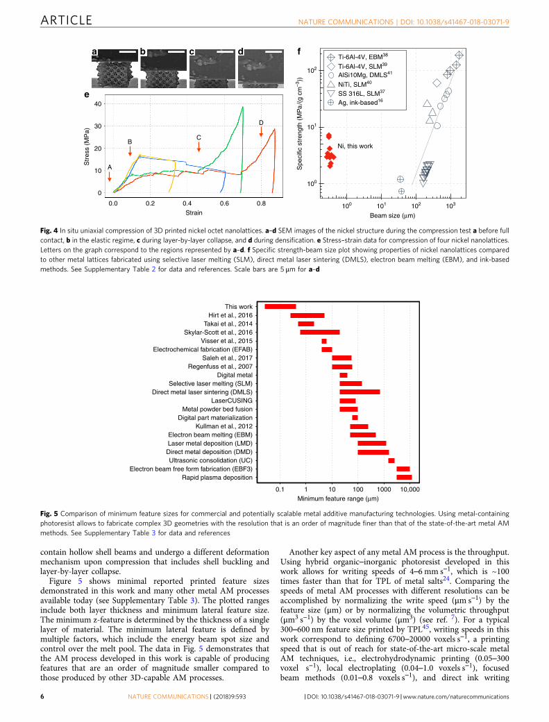
chamber (Quanta 200 FEG, FEI), which enabled observing thedeformation while simultaneously collecting load vs. displace-ment data32 (see Supplementary Movie 1). The collected datawere converted into engineering stresses and strains by dividingthe load by the sample footprint area and dividing the displace-ment by the initial sample height, respectively. Figure 4a–d showsSEM snapshots obtained during a compression experiment of arepresentative sample; stress vs. strain data for four representativesamples are shown in Fig. 4e (data for additional six samples arepresented in Supplementary Fig. 4). All stress–strain data appearto be self-consistent and reproducible. A toe region in the initialportion of each experiment (not shown) is representative ofdeformation before establishing full contact between the sampleand flat punch indenter tip (see Supplementary Fig. 5 for fullstress–strain data). The toe region also included the failure of thesupporting pillar, which allowed for establishing full contactbetween the sample and the substrate.
We found that the stress vs. strain data was typical for cellularsolids compressions, with the characteristic elastic loading,plateau, and densification sections33. The arrows on the plot arecorrelated with the images above and demarcate specific stagesduring compression: initial contact (region A), elastic deforma-tion (region B), layer-by-layer collapse (region C), and densifica-tion (region D). The point of full contact was determined usingharmonic contact stiffness and SEM video. The slope of the elasticloading segment, up to 10–15% strain (region B), was used toestimate structural stiffness of the nanolattices, which rangedfrom ~47 to 174MPa. The strength of Ni nanolattices was definedas the maximum stress prior to the first buckling event, markedby open circles in the data in Fig. 4e, and ranged from 6.9 to 18.2MPa. The elastic region was followed by layer-by-layer collapse
up to 65% strain (region C); two of the four samples wereunloaded at 30 and 60% strain. The two other samples werecompressed to 70–85% strains, reached densification (region D)and then unloaded (see Supplementary Movie 1). None of thenanolattices recovered after deformation.
DiscussionEDS analysis revealed that the fabricated nanolattices have acomposition of 91.8 wt% Ni, 5.0 wt% O, and 3.2 wt% C. It isreasonable to expect traces of carbon in the pyrolyzed structurescaused by the high solubility of carbon in Ni at 1000 °C34, whichleads to carbon precipitation at nickel surface upon cooling downto room temperature. TEM analysis revealed that the carbon alsoexists in the form of 5 nm-sized Ni3C precipitates within thebeams (Fig. 3e). The accuracy of EDS in quantifying the carboncontent may not be sufficient because it is sensitive to the spur-ious carbon deposited in the SEM chamber35. The presence of 5.0wt% O in the nanolattice can be attributed to formation of anative oxide on Ni surface and to full oxidation of small (<6 nm)Ni surface nanoparticles36.
Figure 4f shows the specific strength of Ni nanolatticesfabricated in this work and those of the metallic lattices fabricatedusing other metal AM processes as a function of beam diameteron a log–log plot (see Supplementary Table 2 for details).This plot reveals that the specific strength of metallic lattices inrefs. 16,37–41 decreases by a factor of 280 as the beam diameter isreduced from 1.78 to 0.04 mm, with the lowest reported specificstrength of 0.7 MPa g−1 cm3 for octahedral silver lattices. Nano-crystalline Ni nanolattices in this work have the specific strengthof 2.1–7.2 MPa g−1 cm3, which is ~2–10 times higher than that of
Ni Lα1,2
As printed Pyrolyzed
C Kα1,2
O Kα1
Si Kα1
a
91.75 ± 0.15Ni
Ni
Ni Ni
*Excluding Si
Si
O
C
0 1 2 3 4 5 6 7 8 9 10
Energy (keV)
Inte
nsity
(a.
u.)
Element Wt%*
O
C
5.02 ± 0.08
3.23 ± 0.11
b
c
d
e f
g h
Fig. 2 Energy dispersive spectroscopy (EDS) characterization of fabricated metal nanosctructures. a SEM images of supported 20 μm tetrakaidekahedronunit cell on a Si chip before pyrolysis and b the same structure after pyrolysis (4 μm width). c SEM image of the structure showing where EDS data wascollected. d EDS spectrum taken from an internal beam region reveals chemical composition to be more than 90 wt% nickel. e–h EDS maps show highuniformity of the atomic composition throughout the structure. Scale bars are 5 μm for a, 1 μm for b and 2 μm for c, e–h
ARTICLE NATURE COMMUNICATIONS | DOI: 10.1038/s41467-018-03071-9
4 NATURE COMMUNICATIONS | (2018) 9:593 |DOI: 10.1038/s41467-018-03071-9 |www.nature.com/naturecommunications
octahedral silver lattices with ~40-μm diameter beams16 and~2–7 times higher than the stainless steel lattices with ~200 μmdiameter beams37. It appears to be on the same order as NiTioctahedral lattices with ~250-μm diameter beams40 andAlSi10Mg diamond lattices with ~400 μm beams41. This suggeststhat the AM process developed in this work is capable of pro-ducing architectures with feature sizes that are an order ofmagnitude smaller than those fabricated using existing AMprocesses while retaining high strength. The specific strengthcalculations were performed with the assumption of monolithicbeams, which leads to its underestimation because the nano-crystalline Ni within the beams has 10–30% residual porosity.
Some of the existing literature on the deformation of nano-porous metallic foams42 and individual metallic nano-pillars10,43
report higher strengths upon uniaxial compression than onesreported in this work. The key difference between the strengthreported in this work and those in previous reports is that it isrepresentative of the structural strength of the nanolattice, whereeach beam has heterogeneous porous microstructure, as well aseach nodal junction, and both are subjected to a complex stressstate upon global compression. The microstructure that comprisesnanolattices in this work is nanocrystalline and nanoporous, andhas different levels of hierarchy in the sense that each individualbeam is nanocrystalline and nanoporous, as well as the entirestructure. This microstructure within the individual beams stemsfrom sintering of the Ni nanoparticles after the organic compo-nents volatilize; it's in distinct contrast to the monolithic metallicbeams in all other literature on the deformation of nanoporousmaterials. This microstructure is detrimental to the overall
structural strength in two ways: (1) the additional porosity withineach beam lowers the overall relative density of the architecture,and (2) upon mechanical deformation, each sintered junctionexperiences a local stress state, which creates an effective stressconcentration in the material at an adjacent pore. The pores thatborder these regions of local stress concentrations can be viewedas notches or flaws that serve as locations of failure initiation uponmechanical loads. The distribution of nano-pores in each beamthat comprises the nanolattices in this work leads to a distributionin the local failure strengths, which—in combination with thedetrimental effects of lower relative density and the presence ofjunctions—serves to lower the overall structural strength.
The specific strength of the Ni nano-lattices in this work is50–80% lower than that of Cu meso-lattices with a similar relativedensity reported in ref. 11, which likely stems from the latticestrength being governed by that of the monolithic, fully densebeams with grains spanning full beam width. The strength ofnanoporous Au stochastic foams in ref. 42 was reported to beclose to that of monolithic gold because each ligament is a vir-tually defect-free, single crystalline beam, whose strengthapproaches ideal strength of gold42. These foams have a funda-mentally different microstructure compared to the nanolattices inthis work in that they are stochastic foams with relatively slender,curved single-crystalline pristine beams. A direct comparisonbetween the compressive strengths of nanocrystalline Ninanolattices in this work and those of hollow lattices reported inrefs 12,14,15,32,44 may be misleading, because this work is focusedon solid-beam metallic nanolattices, which deform via compres-sion and plastic flow upon uniaxial compression; the others
(200)
(111)Ni
(220)(220)
(220)NiO
1
19.4 ≤ � ≤ 23.4
5.1 ≤ � ≤ 8.1
0
2
4
6
8
10
12
10 15 20 25 30 35 40
Particle size (nm)
Cou
nts
a
f
b c d
e 2.04Å2.04Å1 Ni
2 Ni3C
3 NiO
(002)
(111)
(111)
2.01Å2.01Å
2.14Å2.14Å2.06Å2.06Å
1.98Å1.98Å2
3
-
(113)
(113)
(006)
(200)
(220)
-
Fig. 3 TEM characterization of the resulting metal structure. a SEM image of nickel beams fabricated directly on a 200-nm thick SiN membrane TEM grid bLow-magnification TEM of a 100 nm nickel beam overhanging the edge of 1.25-μm hole in a SiN membrane. c TEM image of the metal sample region wherethe diffraction pattern was taken. d Electron diffraction pattern shows that the printed beam consists mostly out of nanocrystalline nickel with a smallamount of nickel oxide. e HRTEM image of a printed metal beam. Analysis of atomic plane distances using FFT shows predominantly nanocrystalline nickel(region 1) with some amount of nickel carbide in the interior (region 2) and nickel oxide at the surface (region 3). f Grain size histogram for n= 40 particlesmeasured from a TEM image showing 95% confidence intervals for the mean grain size (μ) and the standard deviation (σ) (see Supplementary Fig. 2 andSupplementary Table 1). Scale bars are 1 μm for a, 100 nm for b, 50 nm for c, and 5 nm for e
NATURE COMMUNICATIONS | DOI: 10.1038/s41467-018-03071-9 ARTICLE
NATURE COMMUNICATIONS | (2018) 9:593 |DOI: 10.1038/s41467-018-03071-9 |www.nature.com/naturecommunications 5
contain hollow shell beams and undergo a different deformationmechanism upon compression that includes shell buckling andlayer-by-layer collapse.
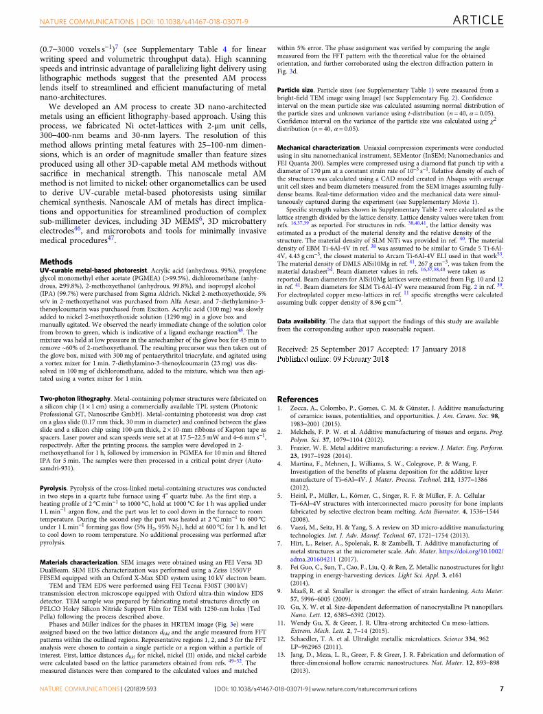
Figure 5 shows minimal reported printed feature sizesdemonstrated in this work and many other metal AM processesavailable today (see Supplementary Table 3). The plotted rangesinclude both layer thickness and minimum lateral feature size.The minimum z-feature is determined by the thickness of a singlelayer of material. The minimum lateral feature is defined bymultiple factors, which include the energy beam spot size andcontrol over the melt pool. The data in Fig. 5 demonstrates thatthe AM process developed in this work is capable of producingfeatures that are an order of magnitude smaller compared tothose produced by other 3D-capable AM processes.
Another key aspect of any metal AM process is the throughput.Using hybrid organic–inorganic photoresist developed in thiswork allows for writing speeds of 4–6 mm s−1, which is ~100times faster than that for TPL of metal salts24. Comparing thespeeds of metal AM processes with different resolutions can beaccomplished by normalizing the write speed (μm s−1) by thefeature size (μm) or by normalizing the volumetric throughput(μm3 s−1) by the voxel volume (μm3) (see ref. 7). For a typical300–600 nm feature size printed by TPL45, writing speeds in thiswork correspond to defining 6700–20000 voxels s−1, a printingspeed that is out of reach for state-of-the-art micro-scale metalAM techniques, i.e., electrohydrodynamic printing (0.05–300voxel s−1), local electroplating (0.04–1.0 voxels s−1), focusedbeam methods (0.01–0.8 voxels s−1), and direct ink writing
This workHirt et al., 2016
Takai et al., 2014Skylar-Scott et al., 2016
Visser et al., 2015Electrochemical fabrication (EFAB)
Saleh et al., 2017Regenfuss et al., 2007
Digital metalSelective laser melting (SLM)
Direct metal laser sintering (DMLS)LaserCUSING
Metal powder bed fusionDigital part materialization
Kullman et al., 2012Electron beam melting (EBM)Laser metal deposition (LMD)Direct metal deposition (DMD)Ultrasonic consolidation (UC)
Electron beam free form fabrication (EBF3)Rapid plasma deposition
0.1 1 10 100Minimum feature range (μm)
1000 10,000
Fig. 5 Comparison of minimum feature sizes for commercial and potentially scalable metal additive manufacturing technologies. Using metal-containingphotoresist allows to fabricate complex 3D geometries with the resolution that is an order of magnitude finer than that of the state-of-the-art metal AMmethods. See Supplementary Table 3 for data and references
Ni, this work
Ti-6Al-4V, EBM38
Ti-6Al-4V, SLM39
AlSi10Mg, DMLS41
NiTi, SLM40
SS 316L, SLM37
Ag, ink-based16
102
101
100
100 101 102
Beam size (μm)
103
cba d
e
f
BC
D
A Spe
cific
str
engt
h (M
Pa
/(g
cm–3
))
40
30
20
10
0
0.0 0.2 0.4 0.6 0.8
Strain
Str
ess
(MP
a)
Fig. 4 In situ uniaxial compression of 3D printed nickel octet nanolattices. a–d SEM images of the nickel structure during the compression test a before fullcontact, b in the elastic regime, c during layer-by-layer collapse, and d during densification. e Stress–strain data for compression of four nickel nanolattices.Letters on the graph correspond to the regions represented by a–d. f Specific strength-beam size plot showing properties of nickel nanolattices comparedto other metal lattices fabricated using selective laser melting (SLM), direct metal laser sintering (DMLS), electron beam melting (EBM), and ink-basedmethods. See Supplementary Table 2 for data and references. Scale bars are 5 μm for a–d
ARTICLE NATURE COMMUNICATIONS | DOI: 10.1038/s41467-018-03071-9
6 NATURE COMMUNICATIONS | (2018) 9:593 |DOI: 10.1038/s41467-018-03071-9 |www.nature.com/naturecommunications
(0.7–3000 voxels s−1)7 (see Supplementary Table 4 for linearwriting speed and volumetric throughput data). High scanningspeeds and intrinsic advantage of parallelizing light delivery usinglithographic methods suggest that the presented AM processlends itself to streamlined and efficient manufacturing of metalnano-architectures.
We developed an AM process to create 3D nano-architectedmetals using an efficient lithography-based approach. Using thisprocess, we fabricated Ni octet-lattices with 2-μm unit cells,300–400-nm beams and 30-nm layers. The resolution of thismethod allows printing metal features with 25–100-nm dimen-sions, which is an order of magnitude smaller than feature sizesproduced using all other 3D-capable metal AM methods withoutsacrifice in mechanical strength. This nanoscale metal AMmethod is not limited to nickel: other organometallics can be usedto derive UV-curable metal-based photoresists using similarchemical synthesis. Nanoscale AM of metals has direct implica-tions and opportunities for streamlined production of complexsub-millimeter devices, including 3D MEMS6, 3D microbatteryelectrodes46, and microrobots and tools for minimally invasivemedical procedures47.
MethodsUV-curable metal-based photoresist. Acrylic acid (anhydrous, 99%), propyleneglycol monomethyl ether acetate (PGMEA) (>99.5%), dichloromethane (anhy-drous, ≥99.8%), 2-methoxyethanol (anhydrous, 99.8%), and isopropyl alcohol(IPA) (99.7%) were purchased from Sigma Aldrich. Nickel 2-methoxyethoxide, 5%w/v in 2-methoxyethanol was purchased from Alfa Aesar, and 7-diethylamino-3-thenoylcoumarin was purchased from Exciton. Acrylic acid (100 mg) was slowlyadded to nickel 2-methoxyethoxide solution (1290 mg) in a glove box andmanually agitated. We observed the nearly immediate change of the solution colorfrom brown to green, which is indicative of a ligand exchange reaction48. Themixture was held at low pressure in the antechamber of the glove box for 45 min toremove ~60% of 2-methoxyethanol. The resulting precursor was then taken out ofthe glove box, mixed with 300 mg of pentaerythritol triacrylate, and agitated usinga vortex mixer for 1 min. 7-diethylamino-3-thenoylcoumarin (23 mg) was dis-solved in 100 mg of dichloromethane, added to the mixture, which was then agi-tated using a vortex mixer for 1 min.
Two-photon lithography. Metal-containing polymer structures were fabricated ona silicon chip (1 × 1 cm) using a commercially available TPL system (PhotonicProfessional GT, Nanoscribe GmbH). Metal-containing photoresist was drop caston a glass slide (0.17 mm thick, 30 mm in diameter) and confined between the glassslide and a silicon chip using 100-μm thick, 2 × 10-mm ribbons of Kapton tape asspacers. Laser power and scan speeds were set at at 17.5–22.5 mW and 4–6 mm s−1,respectively. After the printing process, the samples were developed in 2-methoxyethanol for 1 h, followed by immersion in PGMEA for 10 min and filteredIPA for 5 min. The samples were then processed in a critical point dryer (Auto-samdri-931).
Pyrolysis. Pyrolysis of the cross-linked metal-containing structures was conductedin two steps in a quartz tube furnace using 4″ quartz tube. As the first step, aheating profile of 2 °Cmin−1 to 1000 °C, hold at 1000 °C for 1 h was applied under1 L min−1 argon flow, and the part was let to cool down in the furnace to roomtemperature. During the second step the part was heated at 2 °Cmin−1 to 600 °Cunder 1 L min−1 forming gas flow (5% H2, 95% N2), held at 600 °C for 1 h, and letto cool down to room temperature. No additional processing was performed afterpyrolysis.
Materials characterization. SEM images were obtained using an FEI Versa 3DDualBeam. SEM EDS characterization was performed using a Zeiss 1550VPFESEM equipped with an Oxford X-Max SDD system using 10 kV electron beam.
TEM and TEM EDS were performed using FEI Tecnai F30ST (300 kV)transmission electron microscope equipped with Oxford ultra-thin window EDSdetector. TEM sample was prepared by fabricating metal structures directly onPELCO Holey Silicon Nitride Support Film for TEM with 1250-nm holes (TedPella) following the process described above.
Phases and Miller indices for the phases in HRTEM image (Fig. 3e) wereassigned based on the two lattice distances dhkl and the angle measured from FFTpatterns within the outlined regions. Representative regions 1, 2, and 3 for the FFTanalysis were chosen to contain a single particle or a region within a particle ofinterest. First, lattice distances dhkl for nickel, nickel (II) oxide, and nickel carbidewere calculated based on the lattice parameters obtained from refs. 49–52. Themeasured distances were then compared to the calculated values and matched
within 5% error. The phase assignment was verified by comparing the anglemeasured from the FFT pattern with the theoretical value for the obtainedorientation, and further corroborated using the electron diffraction pattern inFig. 3d.
Particle size. Particle sizes (see Supplementary Table 1) were measured from abright-field TEM image using ImageJ (see Supplementary Fig. 2). Confidenceinterval on the mean particle size was calculated assuming normal distribution ofthe particle sizes and unknown variance using t-distribution (n = 40, α = 0.05).Confidence interval on the variance of the particle size was calculated using χ2
distribution (n = 40, α = 0.05).
Mechanical characterization. Uniaxial compression experiments were conductedusing in situ nanomechanical instrument, SEMentor (InSEM; Nanomechanics andFEI Quanta 200). Samples were compressed using a diamond flat punch tip with adiameter of 170 μm at a constant strain rate of 10–3 s−1. Relative density of each ofthe structures was calculated using a CAD model created in Abaqus with averageunit cell sizes and beam diameters measured from the SEM images assuming fully-dense beams. Real-time deformation video and the mechanical data were simul-taneously captured during the experiment (see Supplementary Movie 1).
Specific strength values shown in Supplementary Table 2 were calculated as thelattice strength divided by the lattice density. Lattice density values were taken fromrefs. 16,37,39 as reported. For structures in refs. 38,40,41, the lattice density wasestimated as a product of the material density and the relative density of thestructure. The material density of SLM NiTi was provided in ref. 40. The materialdensity of EBM Ti-6Al-4V in ref. 38 was assumed to be similar to Grade 5 Ti-6Al-4V, 4.43 g cm−3, the closest material to Arcam Ti-6Al-4V ELI used in that work53.The material density of DMLS AlSi10Mg in ref. 41, 267 g cm−3, was taken from thematerial datasheet54. Beam diameter values in refs. 16,37,38,40 were taken asreported. Beam diameters for AlSi10Mg lattices were estimated from Fig. 10 and 12in ref. 41. Beam diameters for SLM Ti-6Al-4V were measured from Fig. 2 in ref. 39.For electroplated copper meso-lattices in ref. 11 specific strengths were calculatedassuming bulk copper density of 8.96 g cm−3.
Data availability. The data that support the findings of this study are availablefrom the corresponding author upon reasonable request.
Received: 25 September 2017 Accepted: 17 January 2018
References1. Zocca, A., Colombo, P., Gomes, C. M. & Günster, J. Additive manufacturing
of ceramics: issues, potentialities, and opportunities. J. Am. Ceram. Soc. 98,1983–2001 (2015).
2. Melchels, F. P. W. et al. Additive manufacturing of tissues and organs. Prog.Polym. Sci. 37, 1079–1104 (2012).
3. Frazier, W. E. Metal additive manufacturing: a review. J. Mater. Eng. Perform.23, 1917–1928 (2014).
4. Martina, F., Mehnen, J., Williams, S. W., Colegrove, P. & Wang, F.Investigation of the benefits of plasma deposition for the additive layermanufacture of Ti–6Al–4V. J. Mater. Process. Technol. 212, 1377–1386(2012).
5. Heinl, P., Müller, L., Körner, C., Singer, R. F. & Müller, F. A. CellularTi–6Al–4V structures with interconnected macro porosity for bone implantsfabricated by selective electron beam melting. Acta Biomater. 4, 1536–1544(2008).
6. Vaezi, M., Seitz, H. & Yang, S. A review on 3D micro-additive manufacturingtechnologies. Int. J. Adv. Manuf. Technol. 67, 1721–1754 (2013).
7. Hirt, L., Reiser, A., Spolenak, R. & Zambelli, T. Additive manufacturing ofmetal structures at the micrometer scale. Adv. Mater. https://doi.org/10.1002/adma.201604211 (2017).
8. Fei Guo, C., Sun, T., Cao, F., Liu, Q. & Ren, Z. Metallic nanostructures for lighttrapping in energy-harvesting devices. Light Sci. Appl. 3, e161(2014).
9. Maaß, R. et al. Smaller is stronger: the effect of strain hardening. Acta Mater.57, 5996–6005 (2009).
10. Gu, X. W. et al. Size-dependent deformation of nanocrystalline Pt nanopillars.Nano. Lett. 12, 6385–6392 (2012).
11. Wendy Gu, X. & Greer, J. R. Ultra-strong architected Cu meso-lattices.Extrem. Mech. Lett. 2, 7–14 (2015).
12. Schaedler, T. A. et al. Ultralight metallic microlattices. Science 334, 962LP–962965 (2011).
13. Jang, D., Meza, L. R., Greer, F. & Greer, J. R. Fabrication and deformation ofthree-dimensional hollow ceramic nanostructures. Nat. Mater. 12, 893–898(2013).
NATURE COMMUNICATIONS | DOI: 10.1038/s41467-018-03071-9 ARTICLE
NATURE COMMUNICATIONS | (2018) 9:593 |DOI: 10.1038/s41467-018-03071-9 |www.nature.com/naturecommunications 7
14. Montemayor, L. C. & Greer, J. R. Mechanical response of hollow metallicnanolattices: combining structural and material size effects. J. Appl. Mech. 82,71010–71012 (2015).
15. Liontas, R. & Greer, J. R. 3D nano-architected metallic glass: Size effectsuppresses catastrophic failure. Acta Mater. 133, 393–407 (2017).
16. Saleh, M. S., Hu, C. & Panat, R. Three-dimensional microarchitected materialsand devices using nanoparticle assembly by pointwise spatial printing. Sci.Adv. 3, e1601986 (2017).
17. Wang, C.-H., Tsai, H.-L., Wu, Y.-C. & Hwang, W.-S. Investigation of moltenmetal droplet deposition and solidification for 3D printing techniques. J.Micromech. Microeng. 26, 95012 (2016).
18. Taminger, K. M. & Hafley, R. A. Electron beam freeform fabrication for costeffective near-net shape manufacturing. In NATO/RTO AVT-139 Specialists’Meeting on Cost Effective Manufacture via Net Shape Processing 19 (NASALangley Research Center, Hampton, VA, United States, Amsterdam, 2006).
19. Gu, D. D., Meiners, W., Wissenbach, K. & Poprawe, R. Laser additivemanufacturing of metallic components: materials, processes and mechanisms.Int. Mater. Rev. 57, 133–164 (2012).
20. Regenfuss, P. et al. Principles of laser micro sintering. Rapid Prototyp. J. 13,204–212 (2007).
21. Seol, S. K. et al. Electrodeposition-based 3D printing of metallic microarchitectureswith controlled internal structures. Small 11, 3896–3902 (2015).
22. Hirt, L. et al. Template-free 3D microprinting of metals using a force-controlled nanopipette for layer-by-layer electrodeposition. Adv. Mater. 28,2311–2315 (2016).
23. Tanaka, T. Two-photon-induced reduction of metal ions for fabricating three-dimensional electrically conductive metallic microstructure. Appl. Phys. Lett.88, 81107 (2006).
24. Shukla, S., Furlani, E. P., Vidal, X., Swihart, M. T. & Prasad, P. N. Two-photonlithography of sub-wavelength metallic structures in a polymer matrix. Adv.Mater. 22, 3695–3699 (2010).
25. Cohen, A., Chen, R., Frodis, U., Wu, M. & Folk, C. Microscale metal additivemanufacturing of multi‐component medical devices. Rapid Prototyp. J. 16,209–215 (2010).
26. Onses, M. S., Sutanto, E., Ferreira, P. M., Alleyne, A. G. & Rogers, J. A.Mechanisms, capabilities, and applications of high-resolutionelectrohydrodynamic jet printing. Small 11, 4237–4266 (2015).
27. Takai, T., Nakao, H. & Iwata, F. Three-dimensional microfabrication usinglocal electrophoresis deposition and a laser trapping technique. Opt. Express22, 28109–28117 (2014).
28. Skylar-Scott, M. A., Gunasekaran, S. & Lewis, J. A. Laser-assisted direct inkwriting of planar and 3D metal architectures. Proc. Natl. Acad. Sci. 113,6137–6142 (2016).
29. Zenou, M. & Kotler, Z. Printing of metallic 3D micro-objects by laser inducedforward transfer. Opt. Express 24, 1431–1446 (2016).
30. Hon, K. K. B., Li, L. & Hutchings, I. M. Direct writing technology—advancesand developments. CIRP Ann. Manuf. Technol. 57, 601–620 (2008).
31. Wang, D.-W., Li, F., Lu, G. Q. & Cheng, H.-M. Synthesis and dye separationperformance of ferromagnetic hierarchical porous carbon. Carbon N. Y. 46,1593–1599 (2008).
32. Lee, S.-W., Jafary-Zadeh, M., Chen, D. Z., Zhang, Y.-W. & Greer, J. R. Sizeeffect suppresses brittle failure in hollow cu60zr40 metallic glass nanolatticesdeformed at cryogenic temperatures. Nano Lett. 15, 5673–5681 (2015).
33. Gibson, L. J. & Ashby, M. F. Cellular Solids: Structure and Properties 2nd edn(Cambridge University Press, Cambridge, New York, 1997).
34. Lander, J. J., Kern, H. E. & Beach, A. L. Solubility and diffusion coefficient ofcarbon in nickel: reaction rates of nickel‐carbon alloys with barium oxide. J.Appl. Phys. 23, 1305–1309 (1952).
35. Leonard, D. N., Chandler, G. W. & Seraphin, S. in Characterization ofMaterials (Wiley, Hoboken, N.J., 2002).
36. Wang, C.-M. et al. Microstructure of the native oxide layer on Ni and Cr-doped Ni nanoparticles. J. Nanosci. Nanotechnol. 11, 8488–8497 (2011).
37. Tsopanos, S. et al. The influence of processing parameters on the mechanicalproperties of selectively laser melted stainless steel microlattice structures. J.Manuf. Sci. Eng. 132, 41011–41012 (2010).
38. Hernández-Nava, E. et al. The effect of defects on the mechanical response ofTi-6Al-4V cubic lattice structures fabricated by electron beam melting. ActaMater. 108, 279–292 (2016).
39. Challis, V. J. et al. High specific strength and stiffness structures producedusing selective laser melting. Mater. Des. 63, 783–788 (2014).
40. Speirs, M., Van Hooreweder, B., Van Humbeeck, J. & Kruth, J.-P. Fatiguebehaviour of NiTi shape memory alloy scaffolds produced by SLM, a unit celldesign comparison. J. Mech. Behav. Biomed. Mater. 70, 53–59 (2017).
41. Yan, C. et al. Evaluation of light-weight AlSi10Mg periodic cellular latticestructures fabricated via direct metal laser sintering. J. Mater. Process Technol.214, 856–864 (2014).
42. Biener, J. et al. Size effects on the mechanical behavior of nanoporous Au.Nano. Lett. 6, 2379–2382 (2006).
43. Jang, D. & Greer, J. R. Size-induced weakening and grain boundary-assisteddeformation in 60 nm grained Ni nanopillars. Scr. Mater. 64, 77–80 (2011).
44. Meza, L. R., Das, S. & Greer, J. R. Strong, lightweight, and recoverable three-dimensional ceramic nanolattices. Science 345, 1322–1326 (2014).
45. Nanoscribe GmbH. Data sheet, IP-Photoresists. http://www.nanoscribe.de/files/1814/0662/4393/IP-Resist_IP-Dip_web.pdf (Accessed 28th August 2017).
46. Pikul, J. H., Gang Zhang, H., Cho, J., Braun, P. V. & King, W. P. High-powerlithium ion microbatteries from interdigitated three-dimensionalbicontinuous nanoporous electrodes. Nat. Commun. 4, 1732 (2013).
47. Nelson, B. J., Kaliakatsos, I. K. & Abbott, J. J. Microrobots for minimallyinvasive medicine. Annu. Rev. Biomed. Eng. 12, 55–85 (2010).
48. Rozes, L. & Sanchez, C. Titanium oxo-clusters: precursors for a Lego-likeconstruction of nanostructured hybrid materials. Chem. Soc. Rev. 40,1006–1030 (2011).
49. Hu, S. et al. Amorphous TiO2 coatings stabilize Si, GaAs, and GaPphotoanodes for efficient water oxidation. Science 344, 1005–1009 (2014).
50. Chessin, H., Arajs, S. & Colvin, R. V. Paramagnetic susceptibility, electricalresistivity, and lattice parameters of nickel‐rich nickel‐tantalum alloys. J. Appl.Phys. 35, 2419–2423 (1964).
51. Fujieda, S., Shinoda, K., Suzuki, S. & Jeyadevan, B. Synthesis of Ni carbidenanoparticles with Ni3C-type structure in polyol solution containingdispersant. Mater. Trans. 53, 1716–1720 (2012).
52. Tadic, M., Nikolic, D., Panjan, M. & Blake, G. R. Magnetic properties of NiO(nickel oxide) nanoparticles: blocking temperature and Neel temperature. J.Alloys Compd. 647, 1061–1068 (2015).
53. Arcam AB. Ti6Al4V ELI Titanium Alloy Arcam EBM system. http://www.arcam.com/wp-content/uploads/Arcam-Ti6Al4V-ELI-Titanium-Alloy.pdf(Accessed 5th July 2017).
54. EOS GmbH – Electro Optical Systems. Material data sheet. EOS AluminiumAlSi10Mg for EOSINT M 270. https://www.anubis3d.com/documents/dmls/datasheets/Aluminum-AlSi10Mg.pdf (2011).
AcknowledgementsThe authors gratefully acknowledge the financial support of JRG’s Vannevar-BushFaculty Fellowship through the Department of Defense.
Author contributionsA.V., S.D. and J.R.G. conceived the concept. A.V. performed synthesis, fabrication, SEMand EDS characterization. S.D. provided information on how to prepare the photoresist.A.K. performed TEM characterization and analysis. X.Z. and C.M.P. performed nano-compression experiments and analyzed the results. A.V. and J.R.G. wrote the manuscript.All authors commented on the manuscript. J.R.G. supervised the project.
Additional informationSupplementary Information accompanies this paper at https://doi.org/10.1038/s41467-018-03071-9.
Competing interests: The authors declare no competing financial interests.
Reprints and permission information is available online at http://npg.nature.com/reprintsandpermissions/
Publisher's note: Springer Nature remains neutral with regard to jurisdictional claims inpublished maps and institutional affiliations.
Open Access This article is licensed under a Creative CommonsAttribution 4.0 International License, which permits use, sharing,
adaptation, distribution and reproduction in any medium or format, as long as you giveappropriate credit to the original author(s) and the source, provide a link to the CreativeCommons license, and indicate if changes were made. The images or other third partymaterial in this article are included in the article’s Creative Commons license, unlessindicated otherwise in a credit line to the material. If material is not included in thearticle’s Creative Commons license and your intended use is not permitted by statutoryregulation or exceeds the permitted use, you will need to obtain permission directly fromthe copyright holder. To view a copy of this license, visit http://creativecommons.org/licenses/by/4.0/.
© The Author(s) 2018
ARTICLE NATURE COMMUNICATIONS | DOI: 10.1038/s41467-018-03071-9
8 NATURE COMMUNICATIONS | (2018) 9:593 |DOI: 10.1038/s41467-018-03071-9 |www.nature.com/naturecommunications


![Micro -open sets in Micro topology · 2020. 4. 29. · A subset Kof a nano topological space (U,˝ R(X)) is called: 1.nano-regular open if NInt(NCl(K)) = K[14]. 2.nano -open if K](https://static.fdocument.org/doc/165x107/611958b567cf0e3e7d40c138/micro-open-sets-in-micro-topology-2020-4-29-a-subset-kof-a-nano-topological.jpg)