Adapted from notes by ECE 5317-6351 Prof. Jeffery T ...courses.egr.uh.edu/ECE/ECE5317/Class...
25
Prof. David R. Jackson Dept. of ECE Notes 11 ECE 5317-6351 Microwave Engineering Fall 2018 Waveguiding Structures Part 6: Planar Transmission Lines 1 r ε 0 ε h w Adapted from notes by Prof. Jeffery T. Williams
Transcript of Adapted from notes by ECE 5317-6351 Prof. Jeffery T ...courses.egr.uh.edu/ECE/ECE5317/Class...
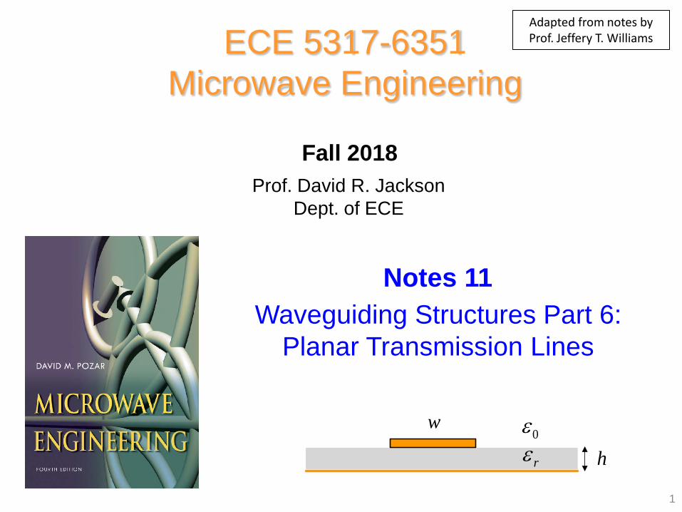
Prof. David R. Jackson Dept. of ECE
Notes 11
ECE 5317-6351 Microwave Engineering
Fall 2018
Waveguiding Structures Part 6: Planar Transmission Lines
1
rε0ε
h
w
Adapted from notes by Prof. Jeffery T. Williams
2
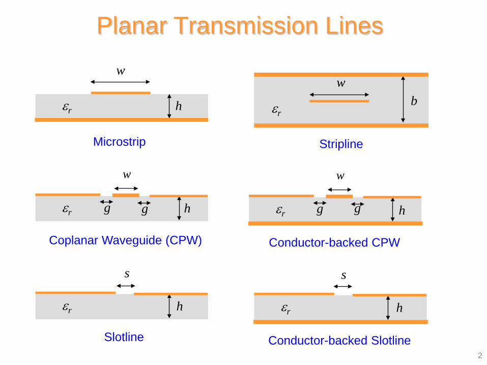
Planar Transmission Lines
εr
Microstrip
w
h εr
Stripline
wb
w
εr
Coplanar Waveguide (CPW)
hgg
w
εr
Conductor-backed CPW
hgg
εr
Slotline
h
s
εr
Conductor-backed Slotline
h
s
3
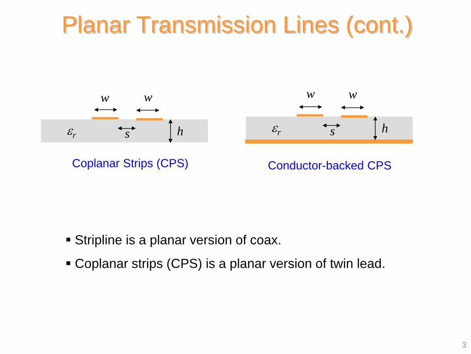
Planar Transmission Lines (cont.)
Stripline is a planar version of coax.
Coplanar strips (CPS) is a planar version of twin lead.
εr
Coplanar Strips (CPS)
h
ww
s εr
Conductor-backed CPS
ww
hs
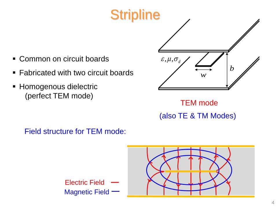
Stripline
Common on circuit boards
Fabricated with two circuit boards
Homogenous dielectric (perfect TEM mode)
Field structure for TEM mode:
(also TE & TM Modes)
TEM mode
4
Electric Field Magnetic Field
, , dε µ σ
wb
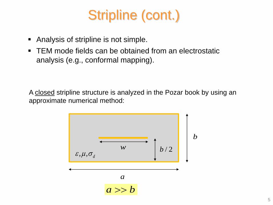
Analysis of stripline is not simple. TEM mode fields can be obtained from an electrostatic
analysis (e.g., conformal mapping).
Stripline (cont.)
5
A closed stripline structure is analyzed in the Pozar book by using an approximate numerical method:
, , dε µ σ
a b>>
wb
/ 2b
a
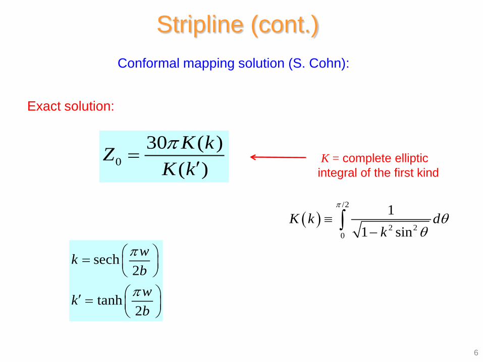
Conformal mapping solution (S. Cohn):
030 ( )
( )K kZ
K kπ
=′
sech2
tanh2
wkbwkb
π
π
= ′ =
K = complete elliptic integral of the first kind
Exact solution:
Stripline (cont.)
6
( )/2
2 20
11 sin
K k dk
π
θθ
≡−∫
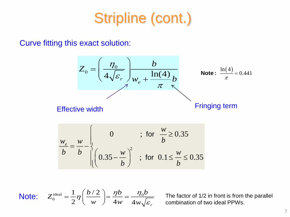
Curve fitting this exact solution:
00 ln(4)4 r
e
bZw b
ηε
π
=
+
Effective width
2
0 ; 0.35
0.35 ; 0.1 0.35
e
wbw w
b b w wb b
≥= − − ≤ ≤
for
for
Stripline (cont.)
ideal 00
1 / 22 4 4 r
bb bZw w w
ηηηε
= = =
Note: The factor of 1/2 in front is from the parallel combination of two ideal PPWs.
( )ln 40.441
π=Note :
7
Fringing term
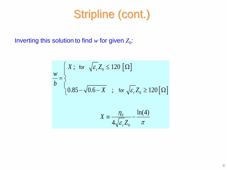
Inverting this solution to find w for given Z0:
[ ]
[ ]
0
0
0
0
; 120
0.85 0.6 ; 120
ln(4)4
r
r
r
X Zwb
X Z
XZ
ε
ε
ηπε
≤ Ω
= − − ≥ Ω
≡ −
for
for
Stripline (cont.)
8
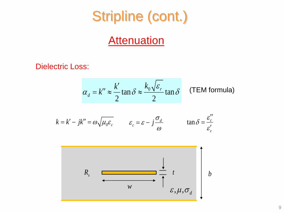
Attenuation
Dielectric Loss:
0tan tan2 2
rd
kkkε
α δ δ′
′′= ≈ ≈
Stripline (cont.)
(TEM formula)
9
0 ck k jk ω µ ε′ ′′= − = dc j σε ε
ω= − tan c
c
εδ
ε′′
=′
, , dε µ σ
b
w
tsR
[ ]
[ ]
3 00
0
00
4(2.7 10 ) ; 120( )
0.16 ; 120
1 21 2 ln( )
1 11 0.414 ln 42 20.7
2
s rr
cs
r
R Z A Zb t
R B ZZ b
w b t b tAb t b t t
b t wBw w tt
ε εη
αε
π
ππ
− × ≤ Ω −= ≥ Ω
+ − = + + − −
= + + + + +
wher
for
for
e 2sR ωµσ
=
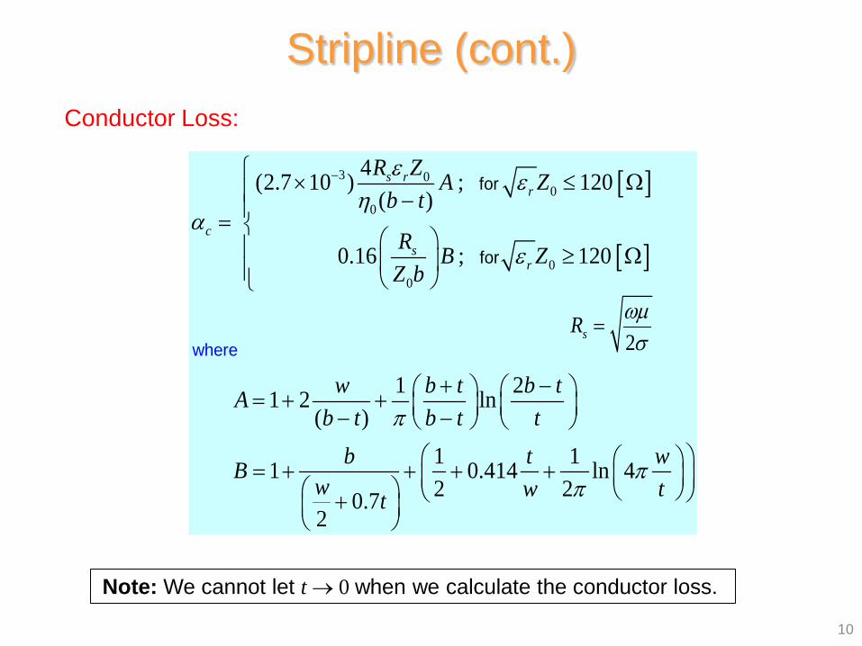
Stripline (cont.) Conductor Loss:
10
Note: We cannot let t → 0 when we calculate the conductor loss.
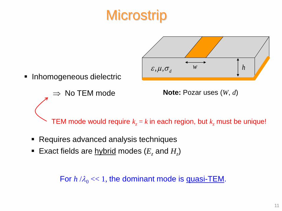
Inhomogeneous dielectric
⇒ No TEM mode
TEM mode would require kz = k in each region, but kz must be unique!
Requires advanced analysis techniques Exact fields are hybrid modes (Ez and Hz)
For h /λ0 << 1, the dominant mode is quasi-TEM.
Microstrip
11
, , dε µ σ
Note: Pozar uses (W, d)
hw
Microstrip (cont.)
12
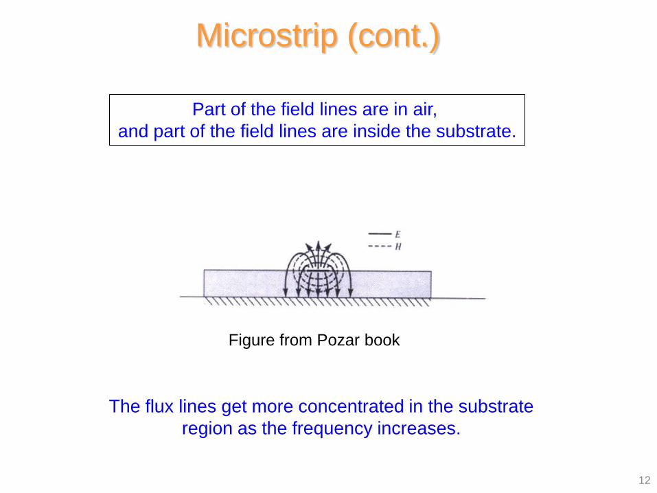
Figure from Pozar book
Part of the field lines are in air, and part of the field lines are inside the substrate.
The flux lines get more concentrated in the substrate region as the frequency increases.
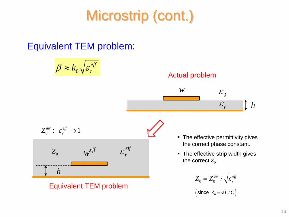
Equivalent TEM problem:
0effrkβ ε≈
Microstrip (cont.)
13
The effective permittivity gives the correct phase constant.
The effective strip width gives the correct Z0.
0 0 /air effrZ Z ε=
( )0 /Z L C=since
Actual problem
rε0ε
h
w
Equivalent TEM problem
effrεeffw
0 : 1air effrZ ε →
0Z
h
1 1 12 2
1 12
eff r rr h
w
ε εε
+ −
= + +
Microstrip (cont.)
14
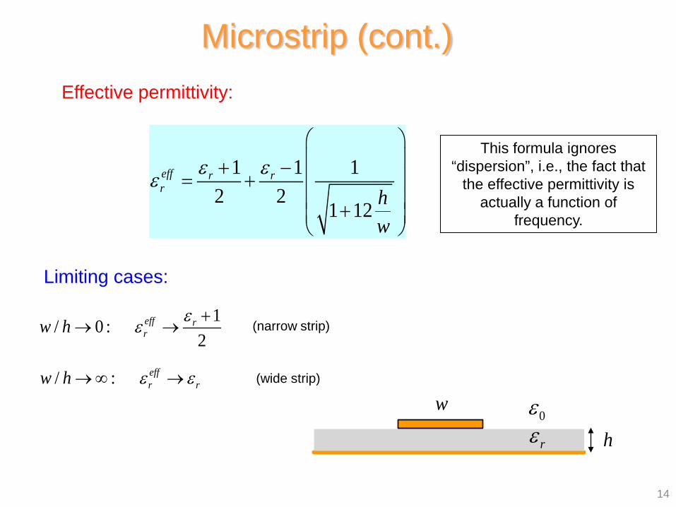
1/ 0 :2
eff rrw h εε +
→ →
/ : effr rw h ε ε→ ∞ →
Effective permittivity:
Limiting cases:
(narrow strip)
(wide strip)
rε0ε
h
w
This formula ignores “dispersion”, i.e., the fact that
the effective permittivity is actually a function of
frequency.
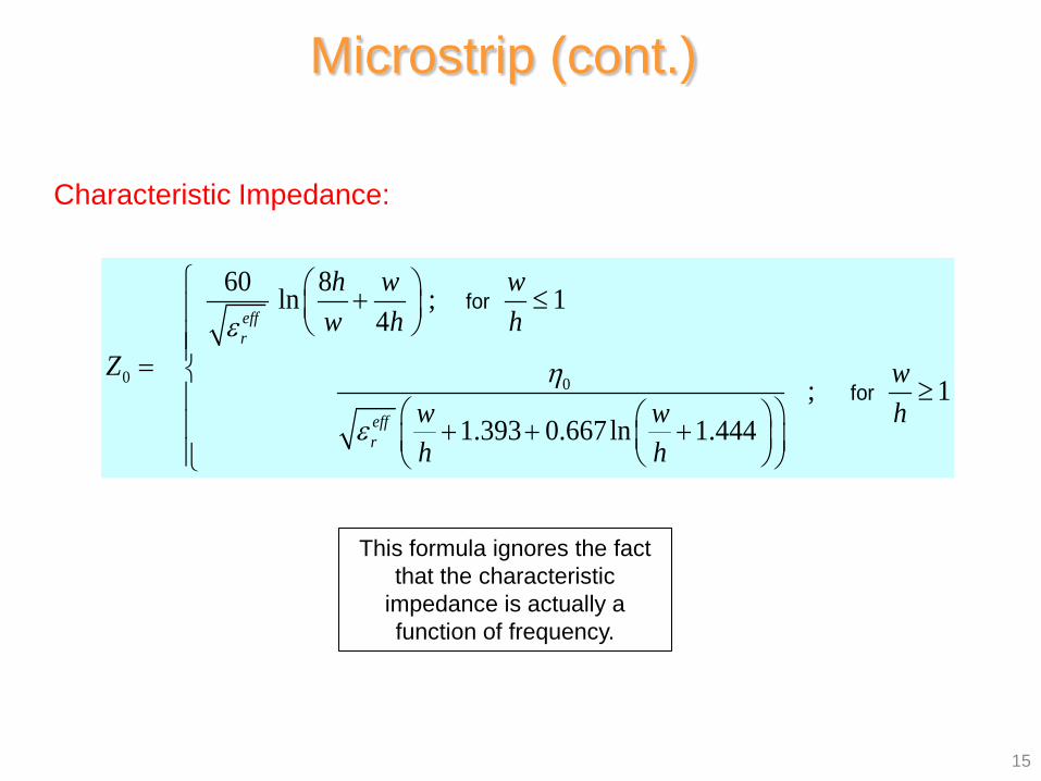
0 0
60 8ln ; 14
; 11.393 0.667ln 1.444
effr
effr
h w ww h h
Z ww w hh h
εη
ε
+ ≤ = ≥ + + +
for
for
Microstrip (cont.)
15
Characteristic Impedance:
This formula ignores the fact that the characteristic
impedance is actually a function of frequency.
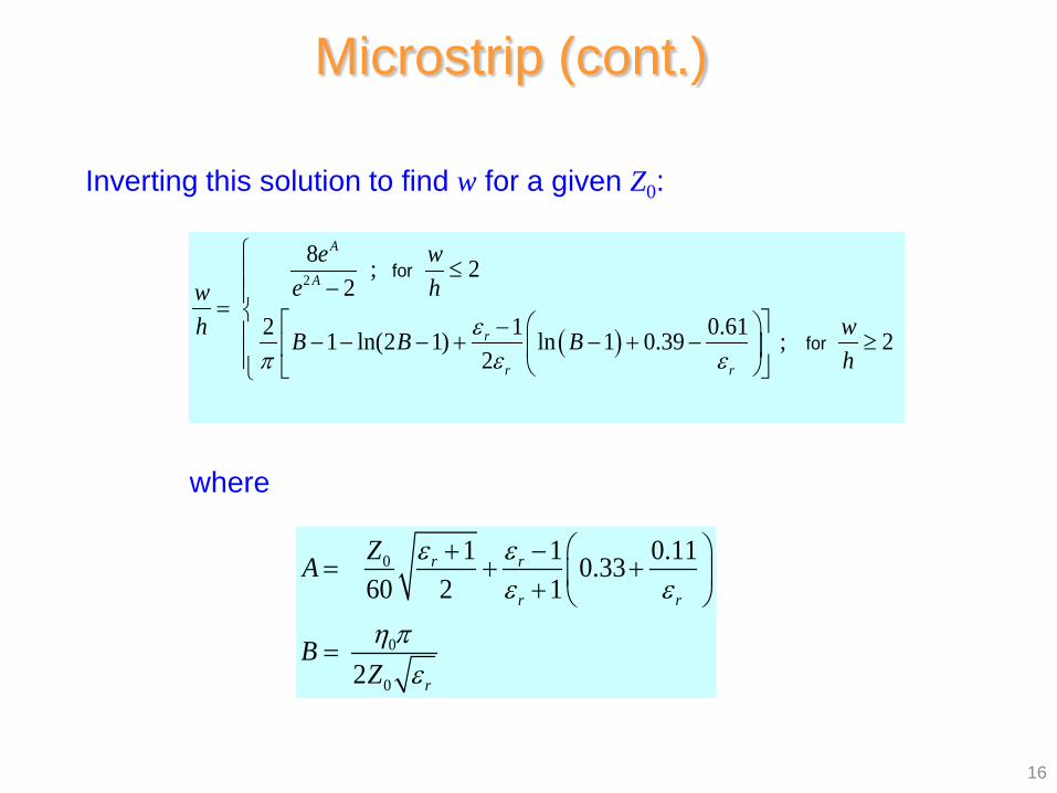
Inverting this solution to find w for a given Z0:
( )
2
8 ; 22
2 1 0.611 ln(2 1) ln 1 0.39 ; 22
A
A
r
r r
e we hw
h wB B Bh
επ ε ε
≤ −= − − − − + − + − ≥
for
for
0
0
0
1 1 0.110.3360 2 1
2
r r
r r
r
ZA
BZ
ε εε ε
η πε
+ −= + + +
=
where
Microstrip (cont.)
16
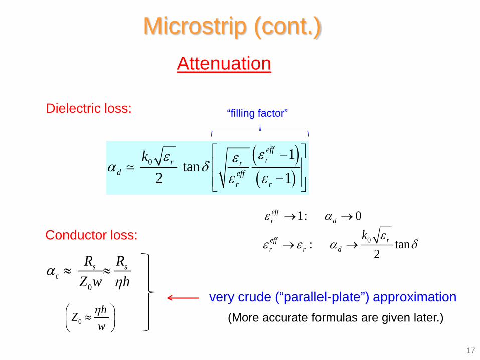
Attenuation
Dielectric loss:
( )( )
01
tan2 1
effrr r
d effr r
k εε εα δε ε
−
−
0
s sc
R RZ w h
αη
≈ ≈
“filling factor”
very crude (“parallel-plate”) approximation
Conductor loss:
Microstrip (cont.)
17
(More accurate formulas are given later.)
1: 0effr dε α→ →
0: tan2
reffr r d
k εε ε α δ→ →
0hZ
wη ≈
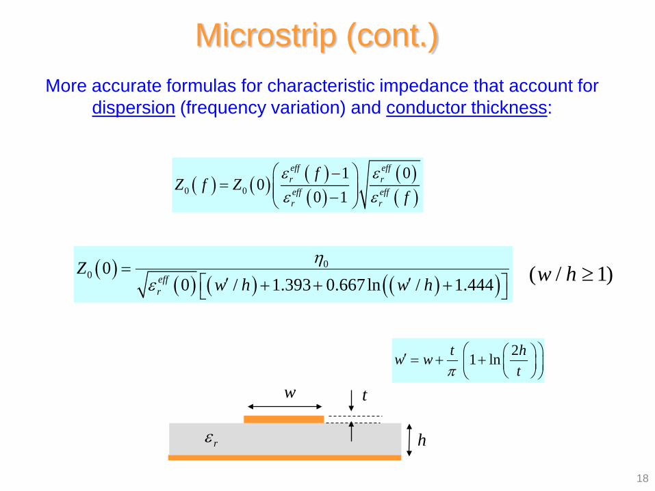
More accurate formulas for characteristic impedance that account for dispersion (frequency variation) and conductor thickness:
( ) ( ) ( )( )
( )( )0 0
1 00
0 1
eff effr reff effr r
fZ f Z
fε εε ε
−= −
( )( ) ( ) ( )( )
00 0
0 / 1.393 0.667ln / 1.444effr
Zw h w h
ηε
= ′ ′+ + +
( / 1)w h ≥
21 lnt hw wtπ
′ = + +
18
Microstrip (cont.)
h
tw
rε
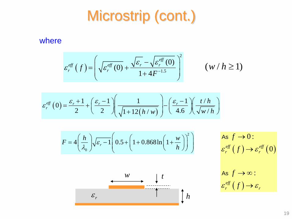
( )2
1.5
(0)(0)
1 4
effr reff eff
r rfF
ε εε ε −
− = + +
( )( )
1 1 1 1 /02 2 4.6 /1 12 /
eff r r rr
t hw hh w
ε ε εε + − − = + − +
2
0
4 1 0.5 1 0.868ln 1rh wF
hε
λ
= − + + +
19
Microstrip (cont.) where
( / 1)w h ≥
Note: ( ) ( )
( )
0 :0
:
eff effr r
effr r
ff
ff
ε ε
ε ε
→
→
→ ∞
→
As
As
h
tw
rε
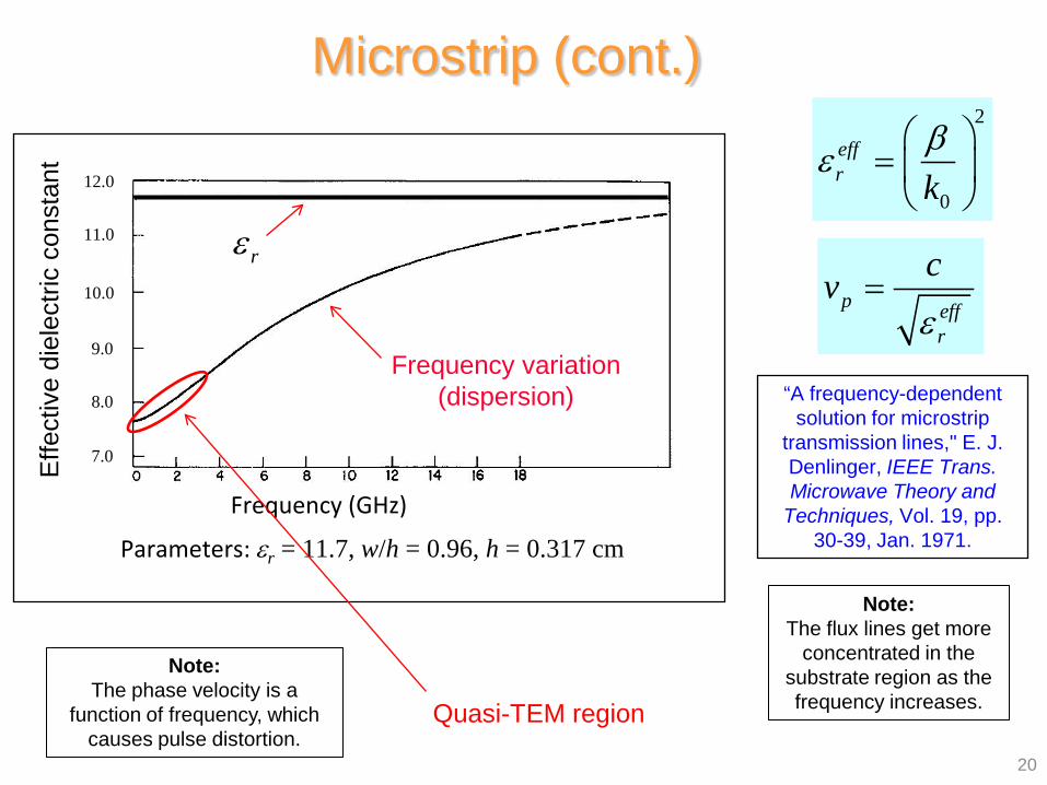
Microstrip (cont.)
20
2
0
effr k
βε
=
“A frequency-dependent solution for microstrip
transmission lines," E. J. Denlinger, IEEE Trans. Microwave Theory and
Techniques, Vol. 19, pp. 30-39, Jan. 1971.
Note: The flux lines get more
concentrated in the substrate region as the frequency increases. Quasi-TEM region
Frequency variation (dispersion)
Effe
ctiv
e di
elec
tric
cons
tant
7.0
8.0
9.0
10.0
11.0
12.0
Parameters: εr = 11.7, w/h = 0.96, h = 0.317 cm
Frequency (GHz)
rε
Note: The phase velocity is a
function of frequency, which causes pulse distortion.
p effr
cvε
=
21
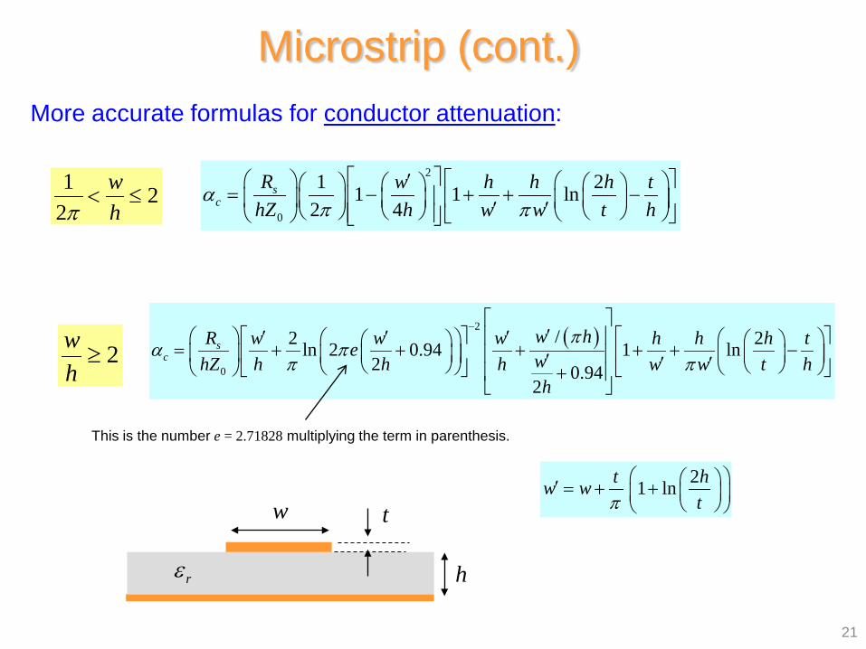
Microstrip (cont.) More accurate formulas for conductor attenuation:
2
0
1 21 1 ln2 4
sc
R w h h h thZ h w w t h
απ π
′ = − + + − ′ ′
1 22
whπ
< ≤
( )2
0
/2 2ln 2 0.94 1 ln2 0.94
2
sc
w hR w w w h h h te whZ h h h w w t hh
πα π
π π
− ′ ′ ′ ′ = + + + + + − ′ ′ ′ +
2wh
≥
21 lnt hw wtπ
′ = + +
This is the number e = 2.71828 multiplying the term in parenthesis.
h
tw
rε
22
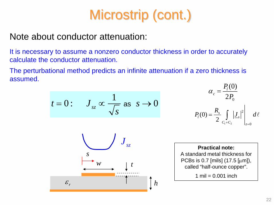
Microstrip (cont.) Note about conductor attenuation:
It is necessary to assume a nonzero conductor thickness in order to accurately calculate the conductor attenuation.
The perturbational method predicts an infinite attenuation if a zero thickness is assumed.
10 : 0szt J ss
= ∝ →as
Practical note: A standard metal thickness for PCBs is 0.7 [mils] (17.5 [µm]),
called “half-ounce copper”.
1 mil = 0.001 inch
0
(0)2l
cP
Pα =
1 2
2
0
(0)2
sl s
C C z
RP J d+ =
= ∫
szJ
h
tw
rε
s

23
TXLINE
This is a public-domain software for calculating the properties of some common planar transmission lines.
http://www.awrcorp.com/products/optional-products/tx-line-transmission-line-calculator
24
TXLINE (cont.)
TX-LINE: Transmission Line Calculator
TX-LINE* software is a FREE and easy-to-use Windows-based interactive transmission line calculator for the analysis and synthesis of transmission line structures. Register and Download Your FREE Copy of TX-LINE Software Today! TX-LINE software enables users to enter either physical or electrical characteristics for common transmission mediums: Microstrip Stripline Coplanar waveguide (WG) Grounded coplanar WG Slotline Learn more: TX-LINE Software Video Demonstration (3 minutes) *Note: TX-LINE software is embedded within NI AWR Design Environment and can be launched from the "Tools" menu.
25
Microstrip (cont.)
REFERENCES L. G. Maloratsky, Passive RF and Microwave Integrated Circuits, Elsevier, 2004. I. Bahl and P. Bhartia, Microwave Solid State Circuit Design, Wiley, 2003.
R. A. Pucel, D. J. Masse, and C. P. Hartwig, “Losses in Microstrip,” IEEE Trans. Microwave Theory and Techniques, pp. 342-350, June 1968. R. A. Pucel, D. J. Masse, and C. P. Hartwig, “Corrections to ‘Losses in Microstrip’,” IEEE Trans. Microwave Theory and Techniques, Dec. 1968, p. 1064.