
A student checks his group lab. CIRCUITS AND SYSTEMS
54
CIRCUITS AND SYSTEMS A student checks his work in the Chandrakasan group lab.
Transcript of A student checks his group lab. CIRCUITS AND SYSTEMS

CIRCUITS AND SYSTEMS
A student checks his
work in the Chandrakasan
group lab.
| C i r C u i t s a n d s y s t e m s
T A B L E O F C O N T E N T SA 77 GHz Front-End Receiver for Antenna Arrays ......................................................................................................................................3A ∆Σ Direct Digital-RF Modulator .............................................................................................................................................................4Outphase Power Amplifiers for OFDM Systems .........................................................................................................................................5Parallel Integrated Receiver Front-Ends for a 5.25 GHz Wireless Gigabit LAN ..............................................................................................6Realization of the Baseband DSP Core for the Wireless Gigabit LAN ...........................................................................................................7An Implementation of a 5.25GHz-Transceiver for the Wireless Gigabit LAN .................................................................................................8Optimization of System and Circuit Parametersin Wideband OFDM Systems ...............................................................................................9Low-Power, High-Speed Analog-To-Digital Converters for Ultra-Wideband Application ...............................................................................10A Pulsed-Based, Ultra-Wideband Transmitter ..........................................................................................................................................11An Ultra-Low-Power Digital Baseband for a Pulsed Ultra-Wideband Transceiver Using Extreme Parallellization ............................................12Ultra-Wideband Baseband and RF Front-ends in SiGe BiCMOS and CMOS ...............................................................................................13Deep Sub-Micron CMOS Analog-To-Digital Conversionfor Ultra-Wideband Radio .......................................................................................14Low-Power RF Transceiver Modeling and Design for Wireless Microsensor Networks ................................................................................15An Ultra Low-Power ADC for Wireless Micro-Sensor Applications .............................................................................................................16A Micropower DSP Architecture for Self-Powered Microsensor Applications ..............................................................................................17An Energy-Efficient RF Transceiver for Wireless Sensor Networks .............................................................................................................18Biasing Techniques for Sub-Threshold MOS Resistive Grids .....................................................................................................................19An Analog Bionic Ear Processor with Zero-Crossing Detection ..................................................................................................................20A 10-nW, 12-Bit Accurate Analog Storage Cell with 10-aA of Leakage .....................................................................................................21Intelligent Human Detection for Night-Vision Systems ............................................................................................................................22Image Fusion for Night-Driving Display ...................................................................................................................................................23Minimum Energy Sub-Threshold Digital Circuits ......................................................................................................................................24Low Energy Digital Circuit Design Using Sub-Threshold Operation ............................................................................................................25Optical-Feedback OLED Display Using Integrated Organic Technology ......................................................................................................26Characterization of Organic Field-Effect Transistors for OLED Displays ......................................................................................................27CMOS-Compatible Compact Display.......................................................................................................................................................28A Low-Power Display Driver with Simultaneous Image Transformation ......................................................................................................29Circuit and System Techniques for On-Chip Interconnects .......................................................................................................................30Evolvable Hardware ...............................................................................................................................................................................313-D FPGA Design and CAD Flow ............................................................................................................................................................32Low-Power FPGA Circuits and CAD ........................................................................................................................................................33Substrate Noise Analysis Tool for Mixed-Signal Verification.......................................................................................................................34Convex Optimization-Aided Design of Analog and Mixed-Signal Communication Systems ..........................................................................35Channel-and-Circuits-Aware, Energy-Efficient Coding for High-Speed Links .............................................................................................36A Massively Parallel High-Speed, Low-Power ADC for WiGLAN ................................................................................................................37Background Self-Calibration of A/D Converters by Direct Transition Point Alignment ..................................................................................38Cartesian Feedback for High-Bandwidth Power Amplifier Linearization .....................................................................................................39Chopper Stabilization in Analog Multipliers ..............................................................................................................................................40Comparator-Based Switched Capacitor Circuits (CBSC) ...........................................................................................................................41Analog-Digital Hybrid Signal Processing and Data Conversion ..................................................................................................................42Digital Implementation and Calibration Technique for High-Speed Continuous-Time Sigma-Delta A/D Converters ........................................43Advanced Delay-Locked Loop Architectures for Chip-To-Chip Communication ..........................................................................................44Optical/Electrical Implementation Techniques for Continuous-Time Sigma-Delta A/D Converters ................................................................45Fast Offset Compensation of High Speed Limit Amplifiers ........................................................................................................................46Techniques for Low-Jitter Clock Multiplication .........................................................................................................................................47Digital Implementation Techniques for High-Performance Clock and Data Recovery Circuits .......................................................................48Low Phase Noise, High Bandwidth Frequency Synthesizer Techniques ......................................................................................................49Test Circuits For IC Variation Assessment ................................................................................................................................................50Variation Analysis and Reduction Techniques for System- and Circuit-Level Design for Manufacturability (DFM) ..........................................51Vibration-to-Electric Energy Harvesting Using a Mechanically-Varied Capacitor .........................................................................................52
m t L a n n u a L r e s e a r C H r e P O r t 0 0 5 |
A 77 GHz Front-End Receiver for Antenna ArraysJ.D. Powell, C.G. Sodini Sponsorship: NSF Fellowship, MIT Lincoln Laboratory
SiGe bipolar technologies have proven to be viable candidates for integrated circuits operating at very high frequencies, due to consistently increasing cutoff frequencies of the transistors. While millimeter wave (MMW) integrated circuits have traditionally been implemented in GaAs or InP, the advancement of silicon technologies has recently enabled silicon-based ICs with promising and cost-effective performance in the MMW regime. The most advanced SiGe bipolar transistors now exhibit cutoff frequencies (fT, fMAX) exceeding 200 GHz, enabling MMW ICs with high levels of integration even between the antenna and front-end radio. Several applications exist for circuits operating in the MMW regime at and above 60 GHz, such as: concealed weapons detection, automotive radar, and high data rate communication systems. Concealed weapons detection is a specific application that improves with increasing frequency due to the distinct difference in radiation between human beings and metals at millimeter wavelengths, which increases the probability of detection. Automotive radar benefits as well from the higher frequency of operation, in that, the spatial resolution is greatly improved over applications at lower frequencies. Another highly useful advantage that comes with radio communication in the MMW regime is the antenna profile. An antenna operating near the silicon interface at 60 GHz on a dielectric such as FR4 requires a length of approximately 1mm. Therefore, an array of 32 x 32 antennas can be fabricated with a small profile of approximately 3 inches2.
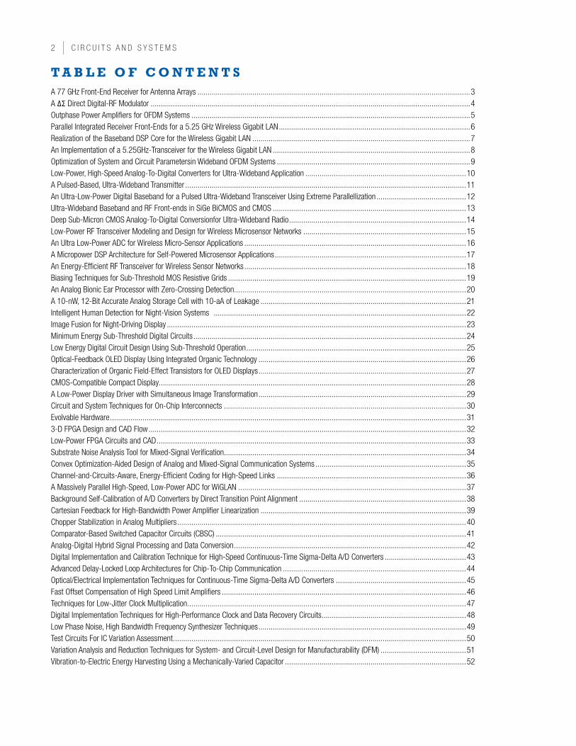
In this research, a 77 GHz front-end receiver will be designed in the IBM 8HP SiGe process for automotive radar applications. The antenna array that will connect directly to the silicon interface will also be designed. Several major circuit design challenges will be encountered at every stage in the front-end receiver, namely: in obtaining a sufficient tuning range in the VCO, achieving sufficient gain in the LNA, and minimizing loading and parasitic capacitance, as it has significant impact on the frequency response of the circuit blocks. The BJT parasitic capacitance also significantly impacts the tuning range of the VCO, since it tends to dominate the varactor capacitance at an oscillation frequency of 77 GHz. This parasitic capacitance will be exploited in the VCO design in order to obtain a superior tuning range. A simple block diagram of the system with the outlining box showing the front end of the receiver is shown in Figure 1 for one of the 1024 antennas that will make up the receiver array. This front-end is part of a typical super-heterodyne receiver with a LO signal of 75 GHz from a fully differential VCO designed for at least a 10% tuning range.
Figure 1: 77 GHz Front- End Receiver Block Diagram
| C i r C u i t s a n d s y s t e m s
A ∆Σ Direct Digital-RF ModulatorA. Jerng, C.G. Sodini Sponsorship: Texas Instruments, MIT Center for Integrated Circuits and Systems
IQ Modulator
DAC
DAC
I
Q
LO 0/90
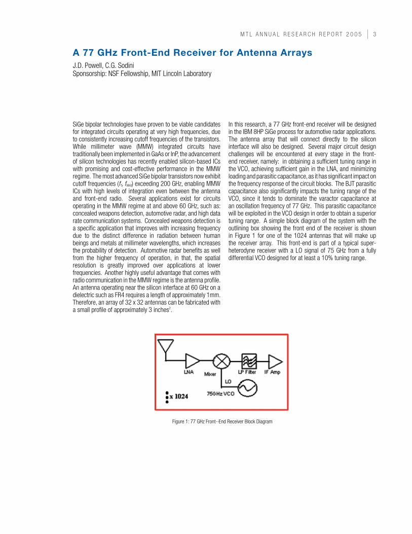
Figure 1: Conventional Transmitter.
t)
+ 1
−+ 1
cos(ω t) ωt)
ωt)(Q+q(t))*sin(
I*cos( ω t)+
0 or 180ο ο
SelectorPhase
SelectorPhase
0 or 180ο ο
∆ Σ
∆ Σ
sin( ω t)
I NyquistFilter
Q NyquistFilter
q(t))*cos((I+
Q*sin(ω
−
Figure 2: Diagram for an IQ ∆Σ Digital-RF Modulator Block.
REFEREncEs:
[1] Luschas, S., R. Schreier, H.S. Lee, “Radio Frequency Digital-to-Analog Converter,” IEEE Journal of Solid-State Circuits, vol. 39, no. 9, pp. 1462-1467, September, 2004.
This research focuses on the implementation of a direct digital-RF transmitter for use in the Wireless Gigabit Local Area Network (WiGLAN) system that is capable of providing a throughput of 1 Gb/s in the 5.15 – 5.35 GHz U-NII bands. This architecture takes advantage of digital process scaling trends by replacing high dynamic range analog circuits with digital circuits.In the conventional IQ transmitter depicted in Figure 1, the I and Q signal paths from the DAC to the output of the analog mixer must maintain noise and distortion to levels satisfying the required dynamic range of the system. As the baseband signal bandwidth increases, the analog anti-aliasing filter consumes more power for the same dynamic range. DAC accuracy becomes degraded by dynamic errors at high frequencies rather than static DC errors. Furthermore, as transistors continue to scale and supply voltages continue to decrease, it becomes more challenging to design high dynamic range analog circuits over a wide bandwidth.Direct digital modulation of an RF carrier can eliminate the DAC, anti-aliasing filter, and analog mixer, resulting in power and area savings. Luschas [1] introduced the RF DAC, which combines a
conventional DAC and mixer into one stage. The RF DAC uses one of the high-frequency Nyquist images of the DAC as an RF output. We further develop this concept by modulating an RF carrier using digitally controlled RF phase shifters. In this way, the output power is concentrated at the RF carrier frequency, rather than at DC and at Nyquist image frequencies. Oversampling ∆Σ concepts are applied to convert digital baseband data into a bitstream of +/- 1’s, corresponding to phase shifts of 0˚ and 180˚. A 2-level RF phase selector can then be implemented using differential signaling and simple CMOS switches. By applying quadrature RF and baseband components to the phase selectors, we create a quadrature digital modulator capable of arbitrary I-Q modulation, as shown in Figure 2. As the noise shaping transfer function (NTF) of the baseband ∆Σ modulators push their quantization noise outside the signal bandwidth, a bandpass filter at the output can remove the up-converted quantization noise, acting as an RF reconstruction filter.The new transmitter architecture requires circuit design in both the digital and RF domains. The main challenges include designing a high-speed digital ∆Σ modulator and realizing a high-Q on-chip passive bandpass filter.
m t L a n n u a L r e s e a r C H r e P O r t 0 0 5 | 5
Outphase Power Amplifiers for OFDM systemsA. Pham, C.G. Sodini Sponsorship: MARCO C2S2
Equation List Figure 1: Outphase Amplifying Block Diagram.
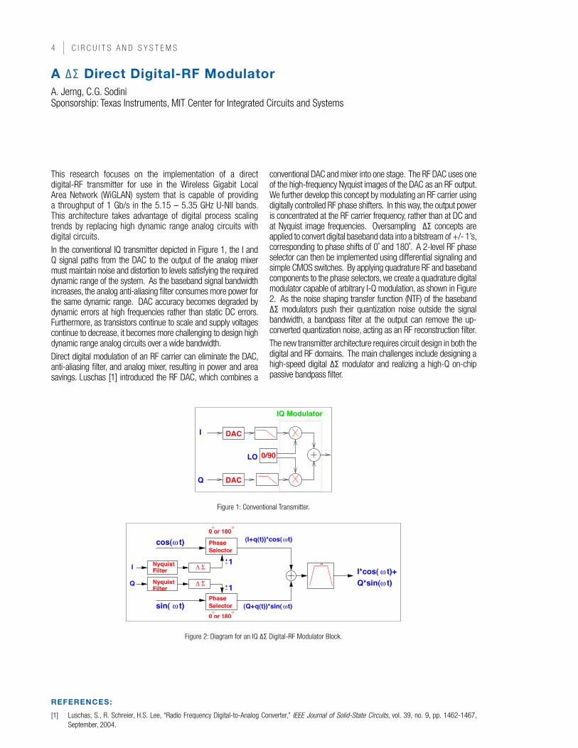
A fundamental trade-off exists between efficiency and linearity among power amplifiers (PAs). Conducting classes such as class-A and -AB offer great linearity, but are very inefficient. On the other hand, switching classes such as class-E and -F have excellent efficiency, but perform poorly in linearity. The outphase amplifying technique allows high-efficiency, non-linear PAs to be used in amplitude-modulated systems that usually require linearity. Originally proposed by Chireix in 1935, the outphase technique uses a simple trigonometric identity, equation (1), to convert an amplitude-modulated signal into two constant-amplitude, phase-modulated signals, as shown in equation (2). The two constant-amplitude signals can then be amplified using two highly efficient, non-linear PAs. Finally, the outputs are combined to restore the original amplitude-modulated signal. A block diagram is shown in Figure 1.The outphase technique’s practical merit depends largely on the implementation of the amplitude-to-phase conversion box. By implementing this function in the digital domain, we can take advantages of the cheap and vast capability of digital technology. However, the amplitude-to-phase conversion,
in general, expands the bandwidth of the original signal. Therefore, the further back we push the conversion from the PAs, the more circuits are affected by bandwidth expansion. In addition, any mismatch in the two outphase paths will cause the combined signal to deviate from the original one and result in transmission errors. This work studies in detail the advantages and challenges of employing the outphase technique for an OFDM system of multiple QAM sub-channels. The amplitude-to-phase conversion is implemented in the digital domain without extra bandwidth constraints on the transmitter analog circuits. A test chip to demonstrate the concepts also includes an on-chip integrated power combiner at 5.8GHz. In addition, system simulations are conducted to find the distribution of OFDM constellations and the link between mismatch and bit-error-rate.
| C i r C u i t s a n d s y s t e m s
Parallel Integrated Receiver Front-Ends for a 5.25 GHz Wireless Gigabit LAnL. Khuon, C.G. Sodini Sponsorship: MARCO C2S2, MIT Center for Integrated Circuits and Systems
Wireless systems with arrays of multiple antennas at the transmitter and receiver promise a greatly increased capacity without increasing the required bandwidth. Going from a “single transmit- single receive” antenna (1x1) system to a “four transmit- four receive” antenna (4x4) system potentially quadruples the achievable data rate; however, each antenna requires a separate analog front-end. Putting each front-end on a separate chip is costly as the number of antennas continues to increase. Integration of the parallel RF chains onto a single chip is a cost-effective solution when both total area and DC power consumption for the multiple front-ends do not increase in proportion to the number of antennas.Using an individual front-end per antenna seems to suggest that the area and DC power consumption increase proportionally with the number of antennas. For example, a receiver with four antennas would consume four times the area and DC power
of a one-antenna receiver; however, large SNR gains, available through spatial diversity with multiple antenna systems, can be used in a variety of tradeoffs to minimize area and DC power consumption. One tradeoff applies SNR gain to lower the necessary transmission power. Another uses the SNR gain to relax the noise requirement of the receiver. The relaxed noise requirement allows physically smaller inductor-less circuits to be used [1], while it minimizes DC power consumption by operating circuits at a lower bias current.
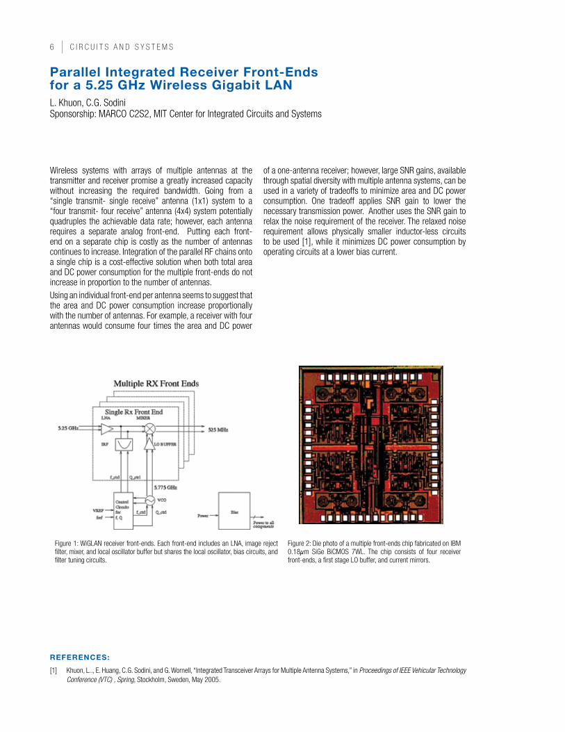
Figure 1: WiGLAN receiver front-ends. Each front-end includes an LNA, image reject filter, mixer, and local oscillator buffer but shares the local oscillator, bias circuits, and filter tuning circuits.
Figure 2: Die photo of a multiple front-ends chip fabricated on IBM 0.18µm SiGe BiCMOS 7WL. The chip consists of four receiver front-ends, a first stage LO buffer, and current mirrors.
REFEREncEs:
[1] Khuon, L.., E. Huang, C.G. Sodini, and G. Wornell, “Integrated Transceiver Arrays for Multiple Antenna Systems,” in Proceedings of IEEE Vehicular Technology Conference (VTC) , Spring, Stockholm, Sweden, May 2005.
m t L a n n u a L r e s e a r C H r e P O r t 0 0 5 |
Realization of the Baseband DsP core for the Wireless Gigabit LAnJ.K. Tan, C.G. Sodini Sponsorship: NSF
In the development of wireless standards, the use of the Orthogonal Frequency Division Multiplexing (OFDM) is becoming increasingly pervasive. The Wireless Gigabit LAN (WiGLAN) aims to achieve a high data rate of 1 Gbps through the utilization of OFDM technology in combination with a wide bandwidth of 150 MHz. The high data rate motivates the need to realize the DSP Core in hardware and test its functionality in real-time. The hardware platform is a Field Programmable Gate Array (FPGA) because it offers programmability and the capability to tradeoff hardware resources for speed. However, even with an FPGA, the implementation of the DSP Core is challenging, because of limited hardware resources and tight real-time requirements. Due to these constraints, the algorithms used in the DSP Core have to be programmed for minimal complexity; algorithms with high complexity take more hardware resources
and lengthen the execution time. After the DSP Core has been realized in hardware, 2 PCs are connected to the DSP Core via PCI to perform high-speed transmission. The goal is to demonstrate a prototype of the WiGLAN’s communication system in which the realized DSP Core will be integrated with the RF Front-End. This test prototype is the primary vehicle for the performance evaluation of the system. The many uses of this prototype include: determining the role of DSP algorithms in mitigating RF imperfections and characterizing the 5-GHz indoor wireless channel.
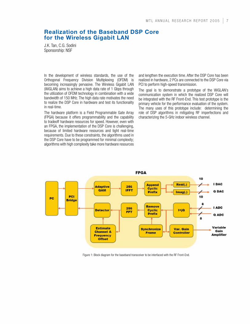
Figure 1: Block diagram for the baseband transceiver to be interfaced with the RF Front-End.
| C i r C u i t s a n d s y s t e m s
An Implementation of a 5.25GHz-Transceiver for the Wireless Gigabit LAnN. Matalon, K.M. Nguyen, C.G. Sodini Sponsorship: NSF
Though the transmission data rate of wireless LAN systems has increased significantly over the past few years with standards today allowing for up to 54 Mbit/s, higher rates are still sought after for a variety of applications. The focus of the Wireless Gigabit LAN (WiGLAN) project is the design of a system capable of transmitting data up to 1Gbit/s. This transmission can be achieved with an OFDM architecture using 150MHz of bandwidth, adaptive modulation per bin, and multiple antennas. This work focuses on the discrete design of the RF front-end used to transmit and receive OFDM symbols already created.The challenge involves successfully transmitting information through a wireless indoor channel while minimizing noise, non-linearity effects, and other system non-idealities. Furthermore, the system should accommodate signal bandwidths up to 150MHz, and operate in the 5.25 GHz band. Low noise figure is desired for increased receiver sensitivity, and linearity must be carefully monitored due to the multi-carrier nature of the
system. Other issues addressed include: 5 GHz impedance matching, preserving gain flatness, synthesizing low spur and low phase noise carriers, and ensuring proper high-speed data conversion.The design is implemented on a printed circuit board and uses the most advanced RF and mixed-signal commercial components. These include: 5 GHz LNAs, filters and mixers; high bandwidth I/Q modulators and demodulators, low-noise variable-gain amplifiers, and high speed (> 250MSPS) 8-10 bit data converters. The synthesis of data converter clocks is also required. Though issues such as power consumption and board area are important and hence, motivate the design of completely integrated systems, this design places a secondary emphasis on these issues and focuses on the implementation of a functioning prototype that will enable the characterization of the wireless channel.
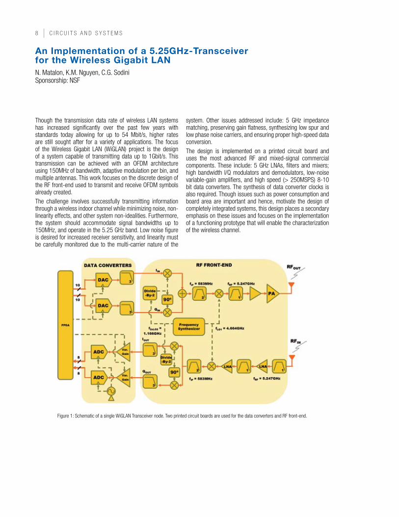
Figure 1: Schematic of a single WiGLAN Transceiver node. Two printed circuit boards are used for the data converters and RF front-end.
m t L a n n u a L r e s e a r C H r e P O r t 0 0 5 |
Optimization of system and circuit Parameters in Wideband OFDM systemsF. Edalat, C.G. Sodini Sponsorship: NSF, Texas Instruments
f
2H
4-QAM
16-QAM64-QAM
256-QAM
Not use
0 5 1 0 1 5 2 0
1 0-4
1 0-3
1 0-2
1 0-1
S N R p e r b it (d B )
BER
2 5 6 -Q A M 6 4 -Q A M
1 6 -Q A M 4 -Q A M B P S K
6.8 10.6 14.8 19.5SNR per bit (dB)
M-Q
AM 256-QAM64-QAM
16-QAM4-QAM
not use
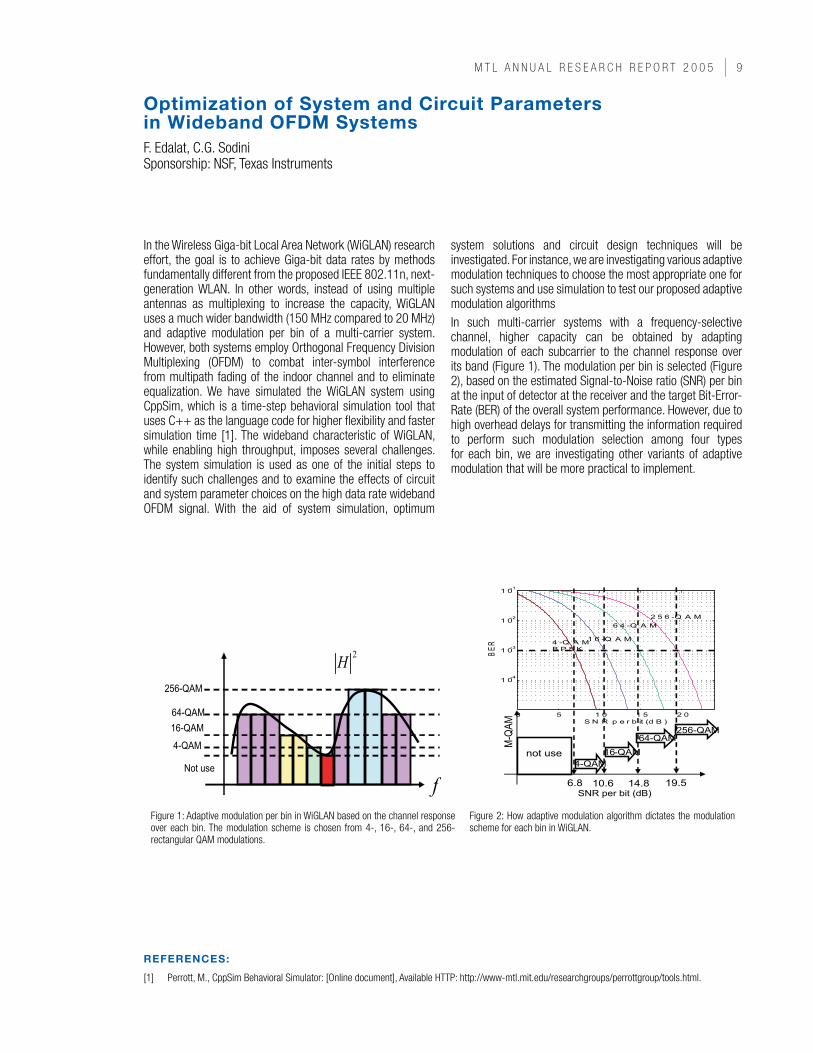
Figure 1: Adaptive modulation per bin in WiGLAN based on the channel response over each bin. The modulation scheme is chosen from 4-, 16-, 64-, and 256-rectangular QAM modulations.
Figure 2: How adaptive modulation algorithm dictates the modulation scheme for each bin in WiGLAN.
REFEREncEs:
[1] Perrott, M., CppSim Behavioral Simulator: [Online document], Available HTTP: http://www-mtl.mit.edu/researchgroups/perrottgroup/tools.html.
In the Wireless Giga-bit Local Area Network (WiGLAN) research effort, the goal is to achieve Giga-bit data rates by methods fundamentally different from the proposed IEEE 802.11n, next-generation WLAN. In other words, instead of using multiple antennas as multiplexing to increase the capacity, WiGLAN uses a much wider bandwidth (150 MHz compared to 20 MHz) and adaptive modulation per bin of a multi-carrier system. However, both systems employ Orthogonal Frequency Division Multiplexing (OFDM) to combat inter-symbol interference from multipath fading of the indoor channel and to eliminate equalization. We have simulated the WiGLAN system using CppSim, which is a time-step behavioral simulation tool that uses C++ as the language code for higher flexibility and faster simulation time [1]. The wideband characteristic of WiGLAN, while enabling high throughput, imposes several challenges. The system simulation is used as one of the initial steps to identify such challenges and to examine the effects of circuit and system parameter choices on the high data rate wideband OFDM signal. With the aid of system simulation, optimum
system solutions and circuit design techniques will be investigated. For instance, we are investigating various adaptive modulation techniques to choose the most appropriate one for such systems and use simulation to test our proposed adaptive modulation algorithmsIn such multi-carrier systems with a frequency-selective channel, higher capacity can be obtained by adapting modulation of each subcarrier to the channel response over its band (Figure 1). The modulation per bin is selected (Figure 2), based on the estimated Signal-to-Noise ratio (SNR) per bin at the input of detector at the receiver and the target Bit-Error-Rate (BER) of the overall system performance. However, due to high overhead delays for transmitting the information required to perform such modulation selection among four types for each bin, we are investigating other variants of adaptive modulation that will be more practical to implement.
1 0 | C i r C u i t s a n d s y s t e m s
Low-Power, High-speed Analog-To-Digital converters for Ultra-Wideband ApplicationA. Chow, H.-S Lee Sponsorship: MARCO C2S2, MIT Center for Integrated Circuits and Systems
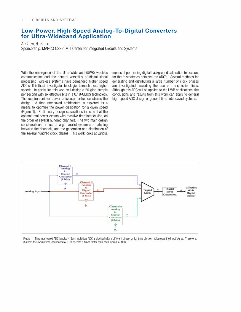
With the emergence of the Ultra-Wideband (UWB) wireless communication and the general versatility of digital signal processing, wireless systems have demanded higher speed ADC’s. This thesis investigates topologies to reach these higher speeds. In particular, this work will design a 20-giga-sample per second with six effective bits in a 0.18-CMOS technology. The requirement for power efficiency further constrains the design. A time-interleaved architecture is explored as a means to optimize the power dissipation for a given speed (Figure 1). Preliminary design calculations indicate that the optimal total power occurs with massive time interleaving, on the order of several hundred channels. The two main design considerations for such a large parallel system are matching between the channels, and the generation and distribution of the several hundred clock phases. This work looks at various
means of performing digital background calibration to account for the mismatches between the ADC’s. Several methods for generating and distributing a large number of clock phases are investigated, including the use of transmission lines. Although this ADC will be applied to the UWB applications, the conclusions and results from this work can apply to general high-speed ADC design or general time-interleaved systems.
Figure 1: Time interleaved ADC topology. Each individual ADC is clocked with a different phase, which time division multiplexes the input signal. Therefore, it allows the overall time-interleaved ADC to operate n times faster than each individual ADC.
m t L a n n u a L r e s e a r C H r e P O r t 0 0 5 | 1 1
A Pulsed-Based, Ultra-Wideband TransmitterD.D. Wentzloff, A.P. Chandrakasan Sponsorship: HP-MIT Alliance, NSF
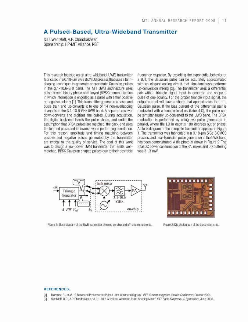
This research focused on an ultra-wideband (UWB) transmitter fabricated in a 0.18-µm SiGe BiCMOS process that uses a tanh-shaping technique to generate approximate Gaussian pulses in the 3.1-10.6-GHz band. The MIT UWB architecture uses pulse-based, binary phase-shift keyed (BPSK) communication in which information is encoded as a pulse with either positive or negative polarity [1]. This transmitter generates a baseband pulse train and up-converts it to one of 14 non-overlapping channels in the 3.1-10.6-GHz UWB band. A separate receiver down-converts and digitizes the pulses. During acquisition, the digital back-end learns the pulse shape, and under the assumption that BPSK pulses are matched, the back-end uses the learned pulse and its inverse when performing correlation. For this reason, amplitude and timing matching between positive and negative pulses generated by the transmitter are critical to the quality of service. The goal of this work was to design a low-power UWB transmitter that emits well-matched, BPSK Gaussian shaped pulses due to their desirable
frequency response. By exploiting the exponential behavior of a BJT, the Gaussian pulse can be accurately approximated with an elegant analog circuit that simultaneously performs up-conversion mixing [2]. The transmitter uses a differential pair with a triangle signal input to generate and shape a pulse of one polarity. For the proper triangle input signal, the output current will have a shape that approximates that of a Gaussian pulse. If the bias current of the differential pair is modulated with a tunable local oscillator (LO), the pulse can be simultaneously up-converted to the UWB band. The BPSK modulation is performed by using two pulse generators in parallel, where the LO in each is 180 degrees out of phase. A block diagram of the complete transmitter appears in Figure 1. The transmitter was fabricated in a 0.18-µm SiGe BiCMOS process, and near-Gaussian pulse generation in the UWB band has been demonstrated. A die photo is shown in Figure 2. The total DC power consumption of the PA, mixer, and LO buffering was 31.3 mW.
Figure 1: Block diagram of the UWB transmitter showing on-chip and off-chip components. Figure 2: Die photograph of the transmitter chip.
REFEREncEs:
[1] Blazquez, R., et al., “A Baseband Processor for Pulsed Ultra-Wideband Signals,” IEEE Custom Integrated Circuits Conference, October 2004.[2] Wentzloff, D.D., A.P. Chandrakasan, “A 3.1-10.6 GHz Ultra-Wideband Pulse-Shaping Mixer,” IEEE Radio Frequency IC Symposium, June 2005.

1 | C i r C u i t s a n d s y s t e m s
An Ultra-Low-Power Digital Baseband for a Pulsed Ultra-Wideband Transceiver Using Extreme ParallellizationV. Sze, R. Blázquez, A.P. Chandrakasan Sponsorship: NSF
Following the developments in UWB communications in the recent years, it has become clear that in order to achieve large data rates in multipath environments, a very complex digital baseband must be used to recover the UWB signal, particularly in the case of long data packets. Of the two IEEE standards currently under development that use UWB signals, this project focuses on the second one, IEEE 802.15.4a.UWB communications are allowed in the 3.1 GHz to 10.6 GHz band with a maximum Equivalent Isotropic Radiated Power of -41.3 dBm/MHz. In this bandwidth, the signal is affected by both an intense multi-path and in-band interferers. Figure 1 shows an example of channel impulse response with an RMS delay of 25 ns based on a modified Saleh-Valenzuela model as recommended by IEEE standard group 802.15.3a.
For this implementation, the metric to optimize is the total energy dissipated to demodulate a very short packet. This optimization can be achieved by using extensive parallelization to reduce the length of the required preamble and also to minimize the clock frequency of the digital circuits. The architecture shown in Figure 2 will be used. This transceiver will be designed to deliver a maximum of 100Mbps using a minimum bandwidth of 500MHz in a 10m-channel for data packets shorter than 500 bits. These specifications make it attractive for sensor networks. An average power of 1mW would be desirable.
Figure 1: Example of multipath impulse response. Figure 2: System level diagram of UWB digital baseband.
REFEREncEs:
[1] Foerster, J., “Channel Modeling Sub-Committee Report Final”, IEEE P802.15 Working Group for Wireless Personal Area Networks (WPANs). February, 2002.
[2] Blázquez, R., A. Chandrakasan, “Architectures for Energy-Aware Impulse UWB Communications”, International Conference on Acoustics, Speech, and Signal Processing, 2005.
m t L a n n u a L r e s e a r C H r e P O r t 0 0 5 | 1
Ultra-Wideband Baseband and RF Front-ends in siGe BicMOs and cMOsF.S. Lee, A.P. Chandrakasan Sponsorship: NSF, HP-MIT Alliance
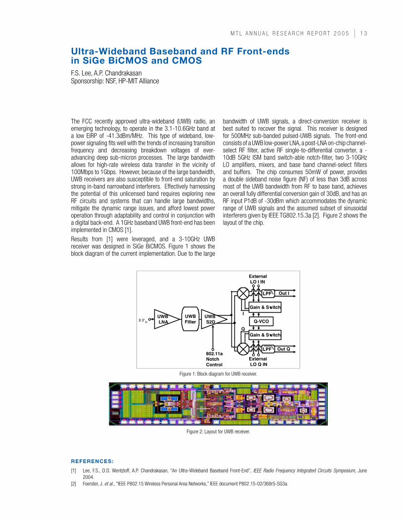
The FCC recently approved ultra-wideband (UWB) radio, an emerging technology, to operate in the 3.1-10.6GHz band at a low EIRP of -41.3dBm/MHz. This type of wideband, low-power signaling fits well with the trends of increasing transition frequency and decreasing breakdown voltages of ever-advancing deep sub-micron processes. The large bandwidth allows for high-rate wireless data transfer in the vicinity of 100Mbps to 1Gbps. However, because of the large bandwidth, UWB receivers are also susceptible to front-end saturation by strong in-band narrowband interferers. Effectively harnessing the potential of this unlicensed band requires exploring new RF circuits and systems that can handle large bandwidths, mitigate the dynamic range issues, and afford lowest power operation through adaptability and control in conjunction with a digital back-end. A 1GHz baseband UWB front-end has been implemented in CMOS [1].Results from [1] were leveraged, and a 3-10GHz UWB receiver was designed in SiGe BiCMOS. Figure 1 shows the block diagram of the current implementation. Due to the large
bandwidth of UWB signals, a direct-conversion receiver is best suited to recover the signal. This receiver is designed for 500MHz sub-banded pulsed-UWB signals. The front-end consists of a UWB low-power LNA, a post-LNA on-chip channel-select RF filter, active RF single-to-differential converter, a -10dB 5GHz ISM band switch-able notch-filter, two 3-10GHz LO amplifiers, mixers, and base band channel-select filters and buffers. The chip consumes 50mW of power, provides a double sideband noise figure (NF) of less than 3dB across most of the UWB bandwidth from RF to base band, achieves an overall fully differential conversion gain of 30dB, and has an RF input P1dB of -30dBm which accommodates the dynamic range of UWB signals and the assumed subset of sinusoidal interferers given by IEEE TG802.15.3a [2]. Figure 2 shows the layout of the chip.
802.11aNotch Control
UWB S2D
UWB LNA
UWBFilter
Gain & Switch
ExternalLO I IN
Out Q
I
Q
RFIN
Out I
LPF
LPF
Gain & Switch
ExternalLO Q IN
Q-VCO
Figure 1: Block diagram for UWB receiver.
Figure 2: Layout for UWB receiver.
REFEREncEs:
[1] Lee, F.S., D.D. Wentzloff, A.P. Chandrakasan, “An Ultra-Wideband Baseband Front-End”, IEEE Radio Frequency Integrated Circuits Symposium, June 2004.
[2] Foerster, J. et al., "IEEE P802.15 Wireless Personal Area Networks,” IEEE document P802.15-02/368r5-SG3a.
1 | C i r C u i t s a n d s y s t e m s
Deep sub-Micron cMOs Analog-To-Digital conversion for Ultra-Wideband RadioB.P. Ginsburg, A.P. Chandrakasan Sponsorship: HP-MIT Alliance, NSF, NDSEG Fellowship
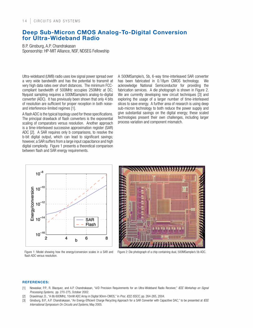
Ultra-wideband (UWB) radio uses low signal power spread over a very wide bandwidth and has the potential to transmit at very high data rates over short distances. The minimum FCC-compliant bandwidth of 500MHz occupies 250MHz at DC; Nyquist sampling requires a 500MSample/s analog-to-digital converter (ADC). It has previously been shown that only 4 bits of resolution are sufficient for proper reception in both noise- and interference-limited regimes [1].A flash ADC is the typical topology used for these specifications. The principal drawback of flash converters is the exponential scaling of comparators versus resolution. Another approach is a time-interleaved successive approximation register (SAR) ADC [2]. A SAR requires only b comparisons, to resolve the b-bit digital output, which can lead to significant savings; however, a SAR suffers from a large input capacitance and high digital complexity. Figure 1 presents a theoretical comparison between flash and SAR energy requirements.
A 500MSample/s, 5b, 6-way time-interleaved SAR converter has been fabricated in 0.18µm CMOS technology. We acknowledge National Semiconductor for providing the fabrication services. A die photograph is shown in Figure 2. We are currently developing new circuit techniques [3] and exploring the usage of a larger number of time-interleaved slices to save energy. A further area of research is using deep sub-micron technology to both reduce the power supply and give substantial savings on the digital energy; these scaled technologies present their own challenges, including larger process variation and component mismatch.
Figure 1: Model showing how the energy/conversion scales in a SAR and flash ADC versus resolution.
Figure 2: Die photograph of a chip containing dual, 500MSample/s 5b ADC.
REFEREncEs:
[1] Newaskar, P.P., R. Blazquez, and A.P. Chandrakasan, “A/D Precision Requirements for an Ultra-Wideband Radio Receiver,” IEEE Workshop on Signal Processing Systems, pp. 270-275, October 2002.
[2] Draxelmayr, D., “A 6b 600MHz, 10mW ADC Array in Digital 90nm-CMOS,” in Proc. IEEE ISSCC, pp. 264-265, 2004.[3] Ginsburg, B.P., A.P. Chandrakasan, “An Energy-Efficient Charge Recycling Approach for a SAR Converter with Capacitive DAC,” to be presented at IEEE
International Symposium On Circuits and Systems, May 2005.

m t L a n n u a L r e s e a r C H r e P O r t 0 0 5 | 1 5
Low-Power RF Transceiver Modeling and Design for Wireless Microsensor networksA.Y. Wang, C.G. Sodini Sponsorship: MIT Center for Integrated Circuits and Systems
The design of wireless microsensor systems has gained increasing importance for a variety of civil and military applications. With the objective of providing short-range connectivity with significant fault tolerance, these systems find usage in such diverse areas as: environmental monitoring, industrial process automation, and field surveillance. The main design objective is to maximize the battery life of the sensor nodes while ensuring reliable operations. To achieve this goal, the microsensor node must be designed in a highly integrated fashion and optimized across all levels of system abstraction.A block diagram of a microsensor node appears in Figure 1. For micro-sensor networks, the RF transceiver dominates the power consumption. A system energy model is developed to take into account the effect of both communications protocols and power consumption of transceiver circuit. Using this model, it is determined that a significant fixed energy cost is associated with short-range giga-Hertz transceivers. This fixed
cost comes from the RF building blocks required to perform up and down conversions. The battery life of the microsensor node can be improved significantly by increasing the data rate, reducing the start-up time, and improving the PA efficiency, as Figure 2 shows. Increasing the data rate drives down the fixed energy cost of the transceiver. Reducing the start-up time decreases the start-up energy overhead. Improving the PA efficiency lowers the energy/bit cost of the power amplifier.
DSP
TX PA
sensor
filter
RX
LO
RF transceiver
105
106
107
108
10-6
10-5
Data Rate (bits/s)
Eo
p (
J)
tstart=120 s, =10%
tstart
=120 s, =70%
tstart=20 s, =10%
tstart=20 s, =70%
Figure 1: Microsensor node architecture. The RF transceiver dominates the power consumption.
Figure 2: At low data rate, fixed cost dominates transceiver energy. At high data rate, start-up and PA energy dominate. The tstart is the start-up time and η is the PA efficiency.
1 | C i r C u i t s a n d s y s t e m s
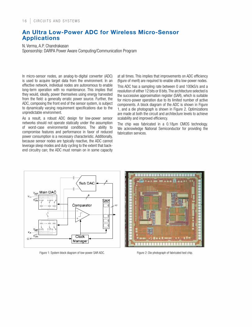
An Ultra Low-Power ADc for Wireless Micro-sensor ApplicationsN. Verma, A.P. Chandrakasan Sponsorship: DARPA Power Aware Computing/Communication Program
In micro-sensor nodes, an analog-to-digital converter (ADC) is used to acquire target data from the environment. In an effective network, individual nodes are autonomous to enable long-term operation with no maintenance. This implies that they would, ideally, power themselves using energy harvested from the field: a generally erratic power source. Further, the ADC, composing the front end of the sensor system, is subject to dynamically varying requirement specifications due to the unpredictable environment.As a result, a robust ADC design for low-power sensor networks should not operate statically under the assumption of worst-case environmental conditions. The ability to compromise features and performance in favor of reduced power consumption is a necessary characteristic. Additionally, because sensor nodes are typically reactive, the ADC cannot leverage sleep modes and duty cycling to the extent that back-end circuitry can; the ADC must remain on in some capacity
at all times. This implies that improvements on ADC efficiency (figure of merit) are required to enable ultra low-power nodes. This ADC has a sampling rate between 0 and 100kS/s and a resolution of either 12 bits or 8 bits. The architecture selected is the successive approximation register (SAR), which is suitable for micro-power operation due to its limited number of active components. A block diagram of the ADC is shown in Figure 1, and a die photograph is shown in Figure 2. Optimizations are made at both the circuit and architecture levels to achieve scalability and improved efficiency.The chip was fabricated in a 0.18µm CMOS technology. We acknowledge National Semiconductor for providing the fabrication services.
Figure 1: System block diagram of low-power SAR ADC. Figure 2: Die photograph of fabricated test chip.
m t L a n n u a L r e s e a r C H r e P O r t 0 0 5 | 1
A Micropower DsP Architecture for self-Powered Microsensor ApplicationsN. Ickes, D. Finchelstein, A.P. Chandrakasan Sponsorship: DARPA Power Aware Computing/Communication Program
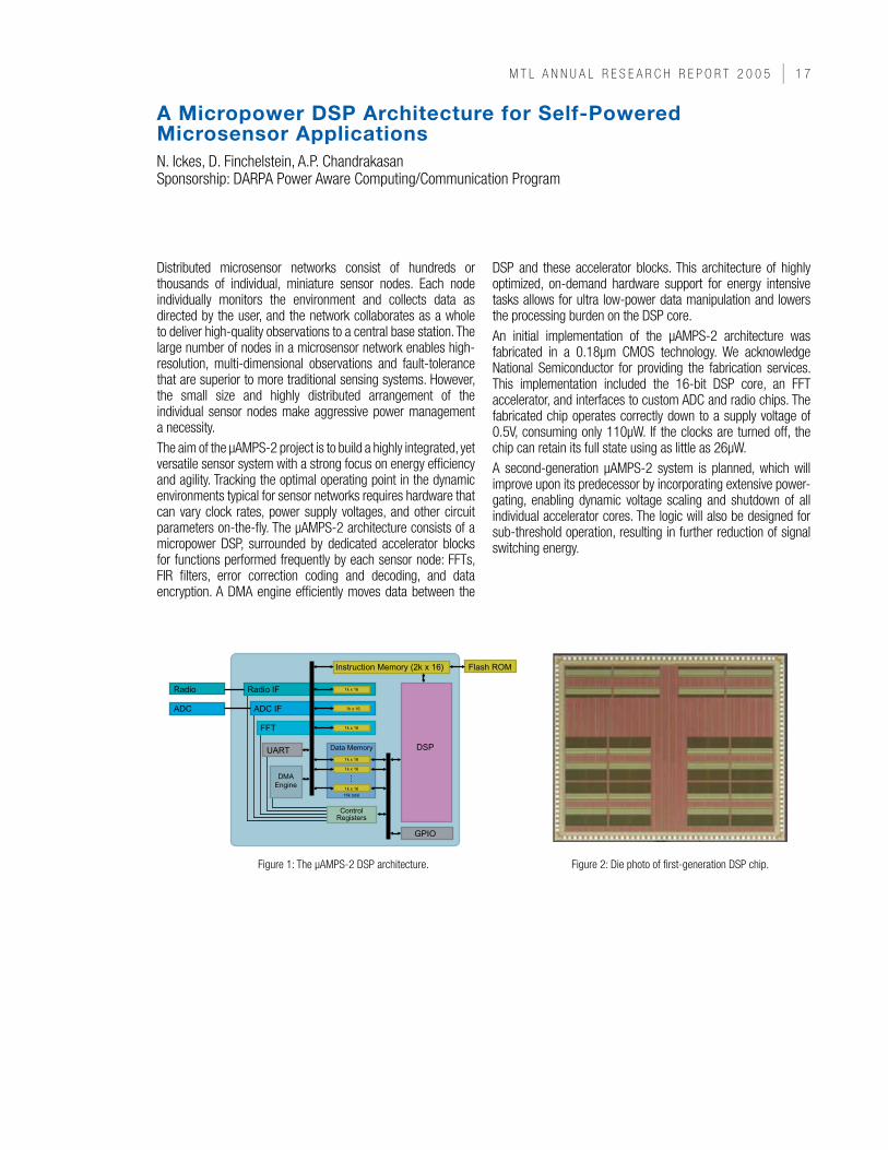
Distributed microsensor networks consist of hundreds or thousands of individual, miniature sensor nodes. Each node individually monitors the environment and collects data as directed by the user, and the network collaborates as a whole to deliver high-quality observations to a central base station. The large number of nodes in a microsensor network enables high-resolution, multi-dimensional observations and fault-tolerance that are superior to more traditional sensing systems. However, the small size and highly distributed arrangement of the individual sensor nodes make aggressive power management a necessity.The aim of the µAMPS-2 project is to build a highly integrated, yet versatile sensor system with a strong focus on energy efficiency and agility. Tracking the optimal operating point in the dynamic environments typical for sensor networks requires hardware that can vary clock rates, power supply voltages, and other circuit parameters on-the-fly. The µAMPS-2 architecture consists of a micropower DSP, surrounded by dedicated accelerator blocks for functions performed frequently by each sensor node: FFTs, FIR filters, error correction coding and decoding, and data encryption. A DMA engine efficiently moves data between the
DSP and these accelerator blocks. This architecture of highly optimized, on-demand hardware support for energy intensive tasks allows for ultra low-power data manipulation and lowers the processing burden on the DSP core. An initial implementation of the µAMPS-2 architecture was fabricated in a 0.18µm CMOS technology. We acknowledge National Semiconductor for providing the fabrication services. This implementation included the 16-bit DSP core, an FFT accelerator, and interfaces to custom ADC and radio chips. The fabricated chip operates correctly down to a supply voltage of 0.5V, consuming only 110µW. If the clocks are turned off, the chip can retain its full state using as little as 26µW. A second-generation µAMPS-2 system is planned, which will improve upon its predecessor by incorporating extensive power-gating, enabling dynamic voltage scaling and shutdown of all individual accelerator cores. The logic will also be designed for sub-threshold operation, resulting in further reduction of signal switching energy.
Radio IF
ADC IF
Data Memory
FFT
Instruction Memory (2k x 16)
UART
DMA Engine
DSP
Flash ROM
GPIO
Control Registers
Radio
ADC
1k x 16
1k x 16
1k x 16
1k x 16
1k x 16
1k x 16
…
16k total
Figure 1: The µAMPS-2 DSP architecture. Figure 2: Die photo of first-generation DSP chip.
1 | C i r C u i t s a n d s y s t e m s
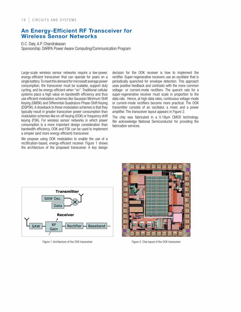
An Energy-Efficient RF Transceiver for Wireless sensor networksD.C. Daly, A.P. Chandrakasan Sponsorship: DARPA Power Aware Computing/Communication Program
Large-scale wireless sensor networks require a low-power, energy-efficient transceiver that can operate for years on a single battery. To meet this demand for microwatt average power consumption, the transceiver must be scalable, support duty cycling, and be energy-efficient when “on”. Traditional cellular systems place a high value on bandwidth efficiency and thus use efficient modulation schemes like Gaussian Minimum Shift Keying (GMSK) and Differential Quadrature Phase-Shift Keying (DQPSK). A drawback to these modulation schemes is that they typically result in greater transceiver power consumption than modulation schemes like on-off keying (OOK) or frequency shift keying (FSK). For wireless sensor networks in which power consumption is a more important design consideration than bandwidth efficiency, OOK and FSK can be used to implement a simpler (and more energy efficient) transceiver.We propose using OOK modulation to enable the use of a rectification-based, energy-efficient receiver. Figure 1 shows the architecture of the proposed transceiver. A key design
decision for the OOK receiver is how to implement the rectifier. Super-regenerative receivers use an oscillator that is periodically quenched for envelope detection. This approach uses positive feedback and contrasts with the more common voltage- or current-mode rectifiers. The quench rate for a super-regenerative receiver must scale in proportion to the data rate. Hence, at high data rates, continuous voltage-mode or current-mode rectifiers become more practical. The OOK transmitter consists of an oscillator, a mixer, and a power amplifier. The transceiver layout appears in Figure 2.The chip was fabricated in a 0.18µm CMOS technology. We acknowledge National Semiconductor for providing the fabrication services.
Figure 1: Architecture of the OOK transceiver Figure 2: Chip layout of the OOK transceiver
m t L a n n u a L r e s e a r C H r e P O r t 0 0 5 | 1
Biasing Techniques for sub-Threshold MOs Resistive GridsK.H. Wee, J.J. Sit, R. Sarpeshkar
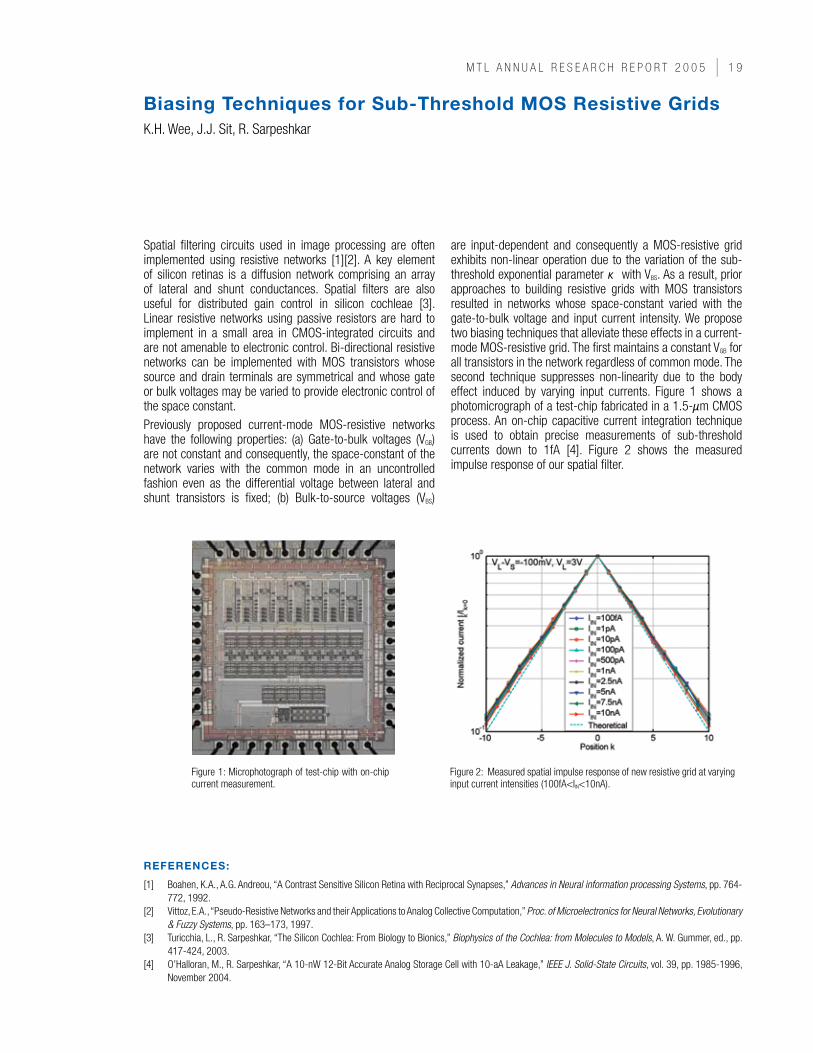
Spatial filtering circuits used in image processing are often implemented using resistive networks [1][2]. A key element of silicon retinas is a diffusion network comprising an array of lateral and shunt conductances. Spatial filters are also useful for distributed gain control in silicon cochleae [3]. Linear resistive networks using passive resistors are hard to implement in a small area in CMOS-integrated circuits and are not amenable to electronic control. Bi-directional resistive networks can be implemented with MOS transistors whose source and drain terminals are symmetrical and whose gate or bulk voltages may be varied to provide electronic control of the space constant. Previously proposed current-mode MOS-resistive networks have the following properties: (a) Gate-to-bulk voltages (VGB) are not constant and consequently, the space-constant of the network varies with the common mode in an uncontrolled fashion even as the differential voltage between lateral and shunt transistors is fixed; (b) Bulk-to-source voltages (VBS)
are input-dependent and consequently a MOS-resistive grid exhibits non-linear operation due to the variation of the sub-threshold exponential parameter κ with VBS. As a result, prior approaches to building resistive grids with MOS transistors resulted in networks whose space-constant varied with the gate-to-bulk voltage and input current intensity. We propose two biasing techniques that alleviate these effects in a current-mode MOS-resistive grid. The first maintains a constant VGB for all transistors in the network regardless of common mode. The second technique suppresses non-linearity due to the body effect induced by varying input currents. Figure 1 shows a photomicrograph of a test-chip fabricated in a 1.5-µm CMOS process. An on-chip capacitive current integration technique is used to obtain precise measurements of sub-threshold currents down to 1fA [4]. Figure 2 shows the measured impulse response of our spatial filter.
Figure 1: Microphotograph of test-chip with on-chip current measurement.
Figure 2: Measured spatial impulse response of new resistive grid at varying input current intensities (100fA<IIN<10nA).
REFEREncEs:
[1] Boahen, K.A., A.G. Andreou, “A Contrast Sensitive Silicon Retina with Reciprocal Synapses,” Advances in Neural information processing Systems, pp. 764-772, 1992.
[2] Vittoz, E.A., “Pseudo-Resistive Networks and their Applications to Analog Collective Computation,” Proc. of Microelectronics for Neural Networks, Evolutionary & Fuzzy Systems, pp. 163–173, 1997.
[3] Turicchia, L., R. Sarpeshkar, “The Silicon Cochlea: From Biology to Bionics,” Biophysics of the Cochlea: from Molecules to Models, A. W. Gummer, ed., pp. 417-424, 2003.
[4] O’Halloran, M., R. Sarpeshkar, “A 10-nW 12-Bit Accurate Analog Storage Cell with 10-aA Leakage,” IEEE J. Solid-State Circuits, vol. 39, pp. 1985-1996, November 2004.
0 | C i r C u i t s a n d s y s t e m s
An Analog Bionic Ear Processor with Zero-crossing DetectionR. Sarpeshkar, M. Baker, C. Salthouse, J.J. Sit, L. Turicchia, S. Zhak Sponsorship: Packard Foundation
Deaf patients with more than 70dB-80dB of hearing loss cannot use a hearing aid and require a cochlear implant. The implant stimulates the auditory nerve with electrical current using 8-20 electrodes surgically implanted in the patient’s cochlea. The stimulation is coded such that logarithmic spectral-energy outputs of an audio filter bank are topographically mapped to the electrode array. For programmability, cochlear implant processing has been done mostly in the digital domain by digitizing the output of a microphone front-end and feeding it to a DSP. However, the microphone front-end, A/D converter, and DSP consume a few mW of power even in very power-efficient systems. In this paper, we report a chip that implements most of the cochlear implant processing in the analog domain and delays digitization to the very end to achieve a power consumption of 251µW, while still leaving room for 750 µW of stimulation power.In the future, an entire cochlear implant will be fully implanted inside the body of the patient and will be required to run on a 100-mAh battery with, at most, 1000 wireless recharges and no battery replacement for, at least, 30 years. This power consumption of this chip is lower than state-of-the-art A/D-then-DSP designs by a factor of 20, and thus, is able to meet the fully-implantable power requirements. The use of analog processing to substantially reduce power in portable systems of moderate complexity appears to be an emerging technology direction, for example, in a recently reported hearing-aid processor [1].
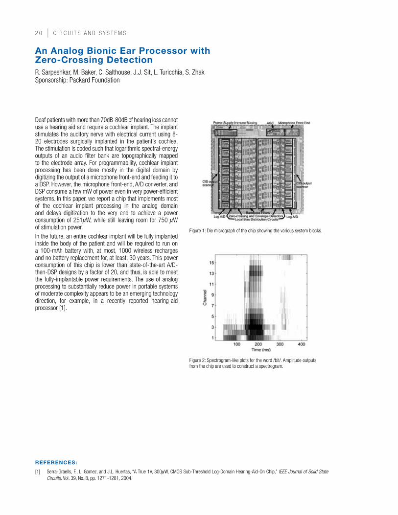
Figure 1: Die micrograph of the chip showing the various system blocks.
Figure 2: Spectrogram-like plots for the word /bit/. Amplitude outputs from the chip are used to construct a spectrogram.
REFEREncEs:
[1] Serra-Graells, F., L. Gomez, and J.L. Huertas, “A True 1V, 300µW, CMOS Sub-Threshold Log-Domain Hearing-Aid-On Chip,” IEEE Journal of Solid State Circuits, Vol. 39, No. 8, pp. 1271-1281, 2004.

m t L a n n u a L r e s e a r C H r e P O r t 0 0 5 | 1
A 10-nW, 12-Bit Accurate Analog storage cell with 10-aA of LeakageM. O’Halloran, R. Sarpeshkar Sponsorship: Center for Bits and Atoms NSF Research Grant, Office of Naval Research, Catalyst Foundation, Packard Foundation, Swartz Foundation
Medium-term analog storage offers a compact, accurate, and low-power method of implementing temporary local memory that can be useful in adaptive circuit applications. The performance of these cells is characterized by the sampling accuracy and voltage droop that can be achieved with a given level of die area and power. Hand calculations suggest past implementations have not achieved minimum voltage droop due to uncompensated MOS leakage mechanisms. In this research, the dominant sources of MOS leakage were experimentally characterized in a standard 1.5-µm CMOS process using an on-chip current integration technique, focusing specifically on the 1fA-to-1aA current range. These measurements revealed an accumulation-mode source-drain coupling mechanism that can easily dominate diode leakage under certain bias conditions, and may have limited previous designs. A simple rule-of-thumb is offered for avoiding this leakage effect, leading
to a novel ultra-low leakage switch topology. A differential storage cell incorporating this new switch achieves an average leakage of 10aA at room temperature, an 8× reduction over past designs. The cell loses one bit of voltage accuracy, 700µV on a 12-bit scale and 11.3mV on an 8-bit scale, in 3.3 minutes and 54 minutes, respectively. This represents a 15× increase in hold time at these voltage accuracies over the lowest-leakage cell to date, in only 92% of the area. Since the leakage is independent of amplifier bias, the cell can operate on as little as 10nW of power. Initial measurements from a 0.5µm implementation of the switch topology demonstrate sub-attoamp leakage levels in this technology, suggesting the leakage of this switch topology decreases, approximately, with the square of process feature size.
Figure 1: Die photograph (2.2mm × 2.2mm). A differential analog storage cell, which exhibits 10aA net leakage current at room temperature, is circled in white.
Figure 2: Differential cell leakage with a 2.5pF hold capacitor.
REFEREncEs:
[1] Vittoz, E., H. Oguey, M.A. Maher, O. Nys, E. Dijkstra, and M. Chevroulet, “Analog Storage of Adjustable Synaptic Weights,” in VLSI Design of Neural Networks, U. Ramacher and U. Rückert, Eds. Norwell, MA: Kluwer, pp. 47-63, 1991.
[2] O’Halloran, M., R. Sarpeshkar, “A 10-nW, 12-Bit, Accurate Analog Storage Cell with 10aA Leakage”, IEEE Journal of Solid-State Circuits, Vol. 39, No. 11, pp. 1985-1996, November 2004.
[3 ] Ehlert, M., H. Klar, “A 12-Bit, Medium-Time Analog Storage Device in a CMOS Standard Process,” IEEE Journal of Solid-State Circuits, Vol. 33, No. 7, pp. 1139-1143, July 1998.
| C i r C u i t s a n d s y s t e m s
Intelligent Human Detection for night-Vision systems Y. Fang, I. Masaki, B.K.P. Horn Sponsorship: MTL Intelligent Transportation Research Center
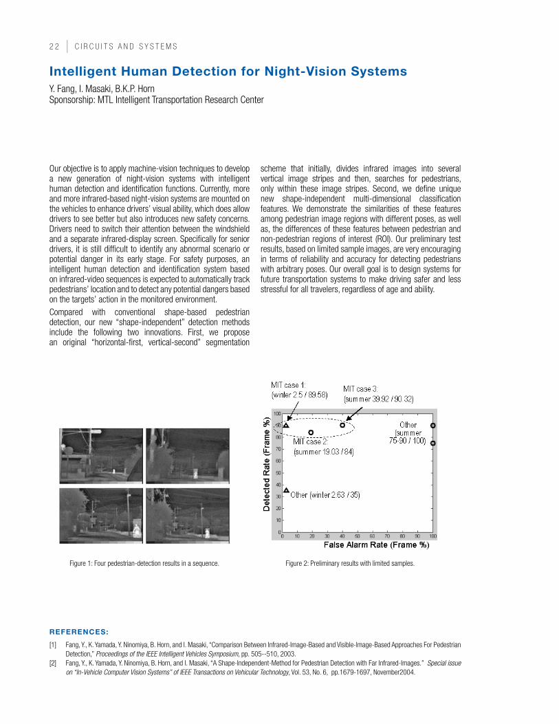
Figure 1: Four pedestrian-detection results in a sequence. Figure 2: Preliminary results with limited samples.
Our objective is to apply machine-vision techniques to develop a new generation of night-vision systems with intelligent human detection and identification functions. Currently, more and more infrared-based night-vision systems are mounted on the vehicles to enhance drivers’ visual ability, which does allow drivers to see better but also introduces new safety concerns. Drivers need to switch their attention between the windshield and a separate infrared-display screen. Specifically for senior drivers, it is still difficult to identify any abnormal scenario or potential danger in its early stage. For safety purposes, an intelligent human detection and identification system based on infrared-video sequences is expected to automatically track pedestrians’ location and to detect any potential dangers based on the targets’ action in the monitored environment.Compared with conventional shape-based pedestrian detection, our new “shape-independent” detection methods include the following two innovations. First, we propose an original “horizontal-first, vertical-second” segmentation
scheme that initially, divides infrared images into several vertical image stripes and then, searches for pedestrians, only within these image stripes. Second, we define unique new shape-independent multi-dimensional classification features. We demonstrate the similarities of these features among pedestrian image regions with different poses, as well as, the differences of these features between pedestrian and non-pedestrian regions of interest (ROI). Our preliminary test results, based on limited sample images, are very encouraging in terms of reliability and accuracy for detecting pedestrians with arbitrary poses. Our overall goal is to design systems for future transportation systems to make driving safer and less stressful for all travelers, regardless of age and ability.
REFEREncEs:
[1] Fang, Y., K. Yamada, Y. Ninomiya, B. Horn, and I. Masaki, “Comparison Between Infrared-Image-Based and Visible-Image-Based Approaches For Pedestrian Detection,” Proceedings of the IEEE Intelligent Vehicles Symposium, pp. 505--510, 2003.
[2] Fang, Y., K. Yamada, Y. Ninomiya, B. Horn, and I. Masaki, “A Shape-Independent-Method for Pedestrian Detection with Far Infrared-Images.” Special issue on “In-Vehicle Computer Vision Systems” of IEEE Transactions on Vehicular Technology, Vol. 53, No. 6, pp.1679-1697, November2004.
m t L a n n u a L r e s e a r C H r e P O r t 0 0 5 |
Image Fusion for night-Driving DisplayW.F. Herrington, B.K.P. Horn, I. Masaki Sponsorship: MTL Intelligent Transportation Research Center
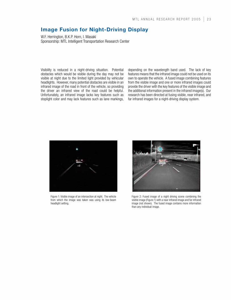
Visibility is reduced in a night-driving situation. Potential obstacles which would be visible during the day may not be visible at night due to the limited light provided by vehicular headlights. However, many potential obstacles are visible in an infrared image of the road in front of the vehicle, so providing the driver an infrared view of the road could be helpful. Unfortunately, an infrared image lacks key features such as stoplight color and may lack features such as lane markings,
depending on the wavelength band used. The lack of key features means that the infrared image could not be used on its own to operate the vehicle. A fused image combining features from the visible image and one or more infrared images could provide the driver with the key features of the visible image and the additional information present in the infrared image(s). Our research has been directed at fusing visible, near infrared, and far infrared images for a night-driving display system.
Figure 1: Visible image of an intersection at night. The vehicle from which the image was taken was using its low-beam headlight setting.
Figure 2: Fused image of a night driving scene combining the visible image (Figure 1) with a near infrared image and far infrared image (not shown). The fused image contains more information than any individual image.
| C i r C u i t s a n d s y s t e m s
Minimum Energy sub-Threshold Digital circuitsY.K. Ramadass, J. Kwong, A.P. Chandrakasan Sponsorship: Texas Instruments, DARPA
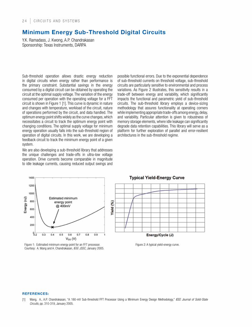
Sub-threshold operation allows drastic energy reduction in digital circuits when energy rather than performance is the primary constraint. Substantial savings in the energy consumed by a digital circuit can be obtained by operating the circuit at the optimal supply voltage. The variation of the energy consumed per operation with the operating voltage for a FFT circuit is shown in Figure 1 [1]. This curve is dynamic in nature and changes with temperature, workload of the circuit, nature of operations performed by the circuit, and data handled. The optimum energy point shifts widely as the curve changes, which necessitates a circuit to track the optimum energy point with changing conditions. The optimal supply voltage for minimum energy operation usually falls into the sub-threshold region of operation of digital circuits. In this work, we are developing a feedback circuit to track the minimum energy point of a given system.We are also developing a sub-threshold library that addresses the unique challenges and trade-offs in ultra-low voltage operation. Drive currents become comparable in magnitude to idle leakage currents, causing reduced output swings and
possible functional errors. Due to the exponential dependence of sub-threshold currents on threshold voltage, sub-threshold circuits are particularly sensitive to environmental and process variations. As Figure 2 illustrates, this sensitivity results in a trade-off between energy and variability, which significantly impacts the functional and parametric yield of sub-threshold circuits. The sub-threshold library employs a device-sizing methodology that assures functionality at operating corners while implementing appropriate trade-offs among energy, delay, and variability. Particular attention is given to robustness of memory storage elements, where idle leakage can significantly degrade data retention capabilities. This library will serve as a platform for further exploration of parallel and error-resilient architectures in the sub-threshold regime.
Figure 1: Estimated minimum energy point for an FFT processor. Courtesy: A. Wang and A. Chandrakasan, IEEE JSSC, January 2005.
Figure 2: A typical yield-energy curve.
REFEREncEs:
[1] Wang, A., A.P. Chandrakasan, “A 180-mV Sub-threshold FFT Processor Using a Minimum Energy Design Methodology,” IEEE Journal of Solid-State Circuits, pp. 310-319, January 2005.
m t L a n n u a L r e s e a r C H r e P O r t 0 0 5 | 5
Low Energy Digital circuit Design Using sub-Threshold OperationB.H. Calhoun, A.P. Chandrakasan Sponsorship: DARPA, Texas Instruments
Scaling of process technologies to smaller dimensions has become a given in the solid-state circuits industry. Recently, process scaling has produced a number of engineering obstacles. Most notably, both active and leakage power of processors are increasing exponentially with technology scaling. For emerging low power applications such as distributed micro-sensor networks or medical applications, low energy operation is the primary concern instead of performance, with the eventual goal of harvesting energy from the environment. Sub-threshold operation has emerged as a promising approach to these ultra-low-energy applications because it achieves the minimum energy per operation. Lowering VDD decreases active energy by VDD
2. For circuits whose leakage energy becomes comparable to the active energy, an optimum VDD for minimum energy operation exists. This optimum typically occurs in the sub-threshold region [1].
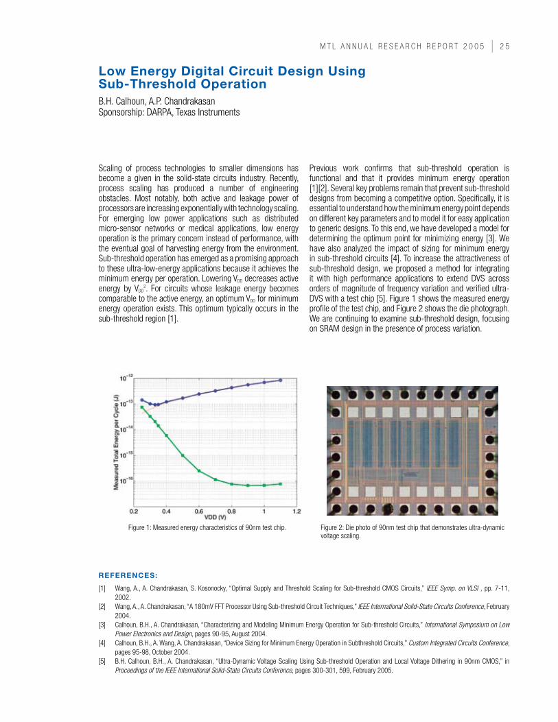
Previous work confirms that sub-threshold operation is functional and that it provides minimum energy operation [1][2]. Several key problems remain that prevent sub-threshold designs from becoming a competitive option. Specifically, it is essential to understand how the minimum energy point depends on different key parameters and to model it for easy application to generic designs. To this end, we have developed a model for determining the optimum point for minimizing energy [3]. We have also analyzed the impact of sizing for minimum energy in sub-threshold circuits [4]. To increase the attractiveness of sub-threshold design, we proposed a method for integrating it with high performance applications to extend DVS across orders of magnitude of frequency variation and verified ultra-DVS with a test chip [5]. Figure 1 shows the measured energy profile of the test chip, and Figure 2 shows the die photograph. We are continuing to examine sub-threshold design, focusing on SRAM design in the presence of process variation.
Figure 1: Measured energy characteristics of 90nm test chip. Figure 2: Die photo of 90nm test chip that demonstrates ultra-dynamic voltage scaling.
REFEREncEs:
[1] Wang, A., A. Chandrakasan, S. Kosonocky, “Optimal Supply and Threshold Scaling for Sub-threshold CMOS Circuits,” IEEE Symp. on VLSI , pp. 7-11, 2002.
[2] Wang, A., A. Chandrakasan, “A 180mV FFT Processor Using Sub-threshold Circuit Techniques,” IEEE International Solid-State Circuits Conference, February 2004.
[3] Calhoun, B.H., A. Chandrakasan, “Characterizing and Modeling Minimum Energy Operation for Sub-threshold Circuits,” International Symposium on Low Power Electronics and Design, pages 90-95, August 2004.
[4] Calhoun, B.H., A. Wang, A. Chandrakasan, “Device Sizing for Minimum Energy Operation in Subthreshold Circuits,” Custom Integrated Circuits Conference, pages 95-98, October 2004.
[5] B.H. Calhoun, B.H., A. Chandrakasan, “Ultra-Dynamic Voltage Scaling Using Sub-threshold Operation and Local Voltage Dithering in 90nm CMOS,” in Proceedings of the IEEE International Solid-State Circuits Conference, pages 300-301, 599, February 2005.
| C i r C u i t s a n d s y s t e m s
Optical-Feedback OLED Display Using Integrated Organic TechnologyK. Lamba, A. Lin, K. Ryu, V. Bulovic, I. Kymissis, C.G. Sodini Sponsorship: MARCO C2S2, MARCO MSD
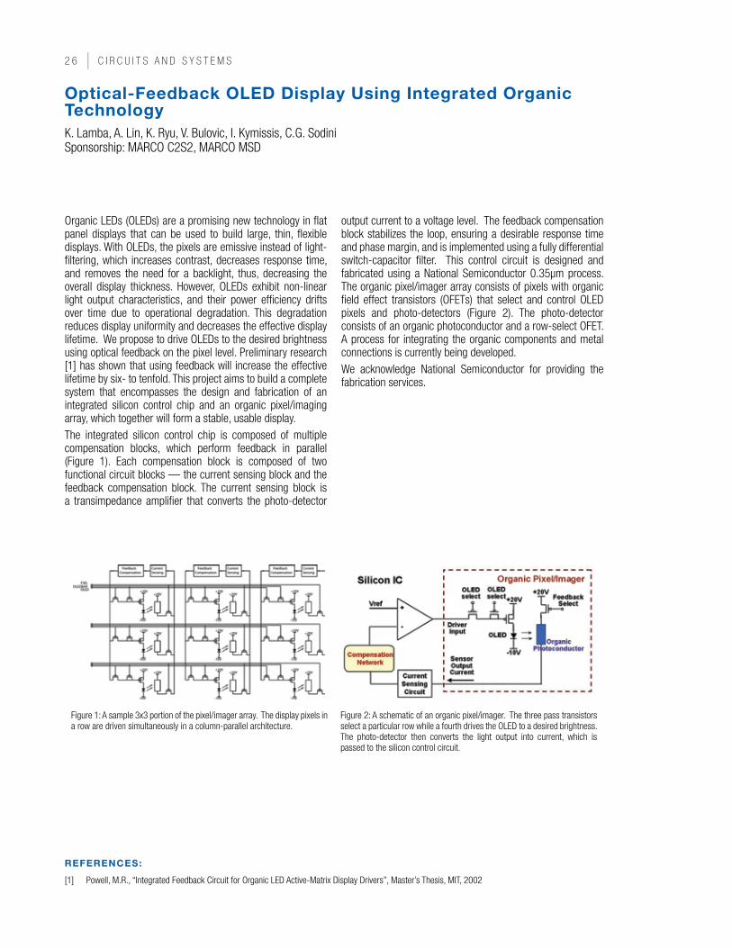
Organic LEDs (OLEDs) are a promising new technology in flat panel displays that can be used to build large, thin, flexible displays. With OLEDs, the pixels are emissive instead of light-filtering, which increases contrast, decreases response time, and removes the need for a backlight, thus, decreasing the overall display thickness. However, OLEDs exhibit non-linear light output characteristics, and their power efficiency drifts over time due to operational degradation. This degradation reduces display uniformity and decreases the effective display lifetime. We propose to drive OLEDs to the desired brightness using optical feedback on the pixel level. Preliminary research [1] has shown that using feedback will increase the effective lifetime by six- to tenfold. This project aims to build a complete system that encompasses the design and fabrication of an integrated silicon control chip and an organic pixel/imaging array, which together will form a stable, usable display.The integrated silicon control chip is composed of multiple compensation blocks, which perform feedback in parallel (Figure 1). Each compensation block is composed of two functional circuit blocks — the current sensing block and the feedback compensation block. The current sensing block is a transimpedance amplifier that converts the photo-detector
output current to a voltage level. The feedback compensation block stabilizes the loop, ensuring a desirable response time and phase margin, and is implemented using a fully differential switch-capacitor filter. This control circuit is designed and fabricated using a National Semiconductor 0.35µm process. The organic pixel/imager array consists of pixels with organic field effect transistors (OFETs) that select and control OLED pixels and photo-detectors (Figure 2). The photo-detector consists of an organic photoconductor and a row-select OFET. A process for integrating the organic components and metal connections is currently being developed.We acknowledge National Semiconductor for providing the fabrication services.
Figure 1: A sample 3x3 portion of the pixel/imager array. The display pixels in a row are driven simultaneously in a column-parallel architecture.
Figure 2: A schematic of an organic pixel/imager. The three pass transistors select a particular row while a fourth drives the OLED to a desired brightness. The photo-detector then converts the light output into current, which is passed to the silicon control circuit.
REFEREncEs:
[1] Powell, M.R., “Integrated Feedback Circuit for Organic LED Active-Matrix Display Drivers”, Master’s Thesis, MIT, 2002
m t L a n n u a L r e s e a r C H r e P O r t 0 0 5 |
characterization of Organic Field-Effect Transistors for OLED DisplaysK. Ryu, I. Kymissis, V. Bulovic, C.G. Sodini Sponsorship: MARCO C2S2
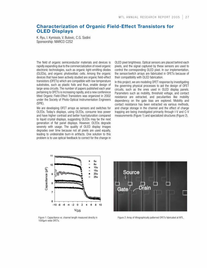
The field of organic semiconductor materials and devices is rapidly expanding due to the commercialization of novel organic electronic technologies, such as organic light-emitting diodes (OLEDs), and organic photovoltaic cells. Among the organic devices that have been actively studied are organic field-effect transistors (OFETs) which are compatible with low temperature substrates, such as plastic foils and thus, enable design of large-area circuits. The number of papers published each year pertaining to OFETs is increasing rapidly, and a new conference titled Organic Field-Effect Transistors was organized in 2002 under the Society of Photo-Optical Instrumentation Engineers (SPIE).We are developing OFET arrays as sensors and switches for OLEDs. Today’s displays, using OLEDs, consume less power and have higher contrast and better hue/saturation compared to liquid crystal displays, suggesting OLEDs may be the next generation of flat panel displays. However, OLEDs degrade severely with usage. The quality of OLED display images degrades over time because not all pixels are used equally, leading to undesirable burn-in artifacts. One solution to this problem is to use optical feedback to correct for the change in
OLED pixel brightness. Optical sensors are placed behind each pixels, and the signal captured by these sensors are used to control the corresponding OLED pixel. In our implementation, the sensor/switch arrays are fabricated in OFETs because of their compatibility with OLED fabrication.In this project, we are modeling OFET response by investigating the governing physical processes to aid the design of OFET circuits, such as the ones used in OLED display panels. Parameters such as mobility, threshold voltage, and contact resistance are extracted, and peculiarities like mobility dependency on the gate bias are explored. Mobility and contact resistance has been extracted via various methods, and charge storage in the channel and the effect of charge trapping are being investigated primarily through I-V and C-V measurements (Figure 1) and specialized structures (Figure 2).
Figure 1: Capacitance vs. channel length measured directly in 1000µm-wide OFETs.
Figure 2: Array of lithographically patterned OFETs fabricated at MTL.
| C i r C u i t s a n d s y s t e m s
cMOs-compatible compact DisplayA.R. Chen, A.I. Akinwande, H.-S. LeeSponsorship: MARCO C2S2
Portable information devices demand displays with high resolution and high image quality that are increasingly compact and energy-efficient. Microdisplays, consisting of a silicon CMOS backplane integrated with light- generating or -modifying devices, are being developed for direct-view and projection applications.Toward the goal of a micro-projector suitable for portable applications, a microdisplay architecture, using silicon light emitters and image intensification, is developed. A standard low-voltage CMOS IC incorporating display drivers and an array of avalanche diodes produces a faint optical image, and an image intensifier efficiently amplifies the image to useful brightness. This architecture has high efficiency and the potential to achieve adequate luminance for projection applications. A proof-of-concept system with 16x32 arrays is implemented and evaluated.
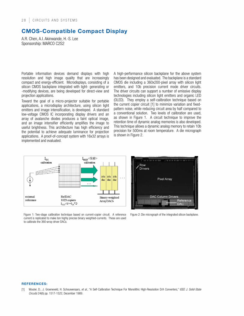
A high-performance silicon backplane for the above system has been designed and evaluated. The backplane is a standard CMOS die including a 360x200-pixel array with silicon light emitters, and 10b precision current mode driver circuits. The driver circuits can support a number of emissive display technologies including silicon light emitters and organic LED (OLED). They employ a self-calibration technique based on the current copier circuit [1] to minimize variation and fixed-pattern noise, while reducing circuit area by half compared to a conventional solution. Two levels of calibration are used, as shown in Figure 1. A circuit technique to improve the retention time of dynamic analog memories is also developed. This technique allows a dynamic analog memory to retain 10b precision for 500ms at room temperature. A die micrograph is shown in Figure 2.
REFEREncEs:
[1] Wouter, D., J. Groeneveld, H. Schouwenaars, et al., “A Self-Calibration Technique For Monolithic High-Resolution D/A Converters,” IEEE J. Solid-State Circuits 24(6) pp. 1517-1522, December 1989.
Figure 1: Two-stage calibration technique based on current-copier circuit. A reference current is replicated to make ten highly precise binary weighted-currents. These are used to calibrate the 360 array driver DACs.
Figure 2: Die micrograph of the integrated silicon backplane.
m t L a n n u a L r e s e a r C H r e P O r t 0 0 5 |
A Low-Power Display Driver with simultaneous Image TransformationJ. Walker, A.P. Chandrakhasan, A.I. Akinwande Sponsorship: DARPA, Army Natick Soldier System Center
While multimedia-enabled mobile devices have recently exploded into mainstream commercial use, two major, and often conflicting, demands exist in displays for mobile devices: low power and high quality. High-quality multimedia applications demand high-resolution screens capable for displaying fast-moving images. Unfortunately, the higher the resolution and the rate of change of the images, the more energy is required to process and display them. Not only is more energy required, but higher bandwidth is also necessary since more data must be processed in a fixed amount of time. While displays for mobile devices are the first to deal with energy and bandwidth requirements, it is easy to see that as displays move to higher resolution, these concerns begin to affect all displays. For example, a standard VGA screen has 640x480 pixels (307,200). A refresh rate of 100 Hz and 8-bits per pixel requires a data rate of 250 Mb/s. A higher definition screen of 6400x4800 pixels at a refresh rate of 100 Hz and 8-bits per pixel would require a data rate of 25 Gb/s . This bandwidth requirement increases as N2 where N is the number
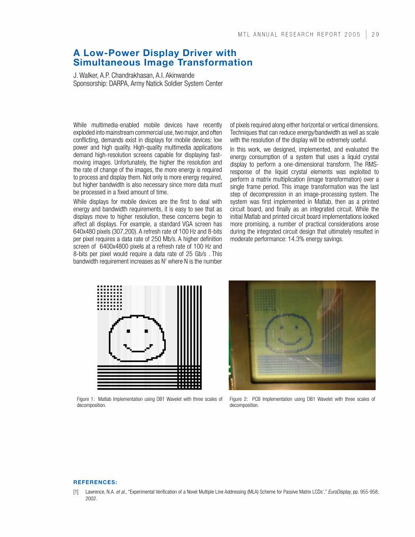
of pixels required along either horizontal or vertical dimensions. Techniques that can reduce energy/bandwidth as well as scale with the resolution of the display will be extremely useful.In this work, we designed, implemented, and evaluated the energy consumption of a system that uses a liquid crystal display to perform a one-dimensional transform. The RMS-response of the liquid crystal elements was exploited to perform a matrix multiplication (image transformation) over a single frame period. This image transformation was the last step of decompression in an image-processing system. The system was first implemented in Matlab, then as a printed circuit board, and finally as an integrated circuit. While the initial Matlab and printed circuit board implementations looked more promising, a number of practical considerations arose during the integrated circuit design that ultimately resulted in moderate performance: 14.3% energy savings.
Figure 1: Matlab Implementation using DB1 Wavelet with three scales of decomposition.
Figure 2: PCB Implementation using DB1 Wavelet with three scales of decomposition.
REFEREncEs:
[1] Lawrence, N.A. et al., “Experimental Verification of a Novel Multiple Line Addressing (MLA) Scheme for Passive Matrix LCDs’,” EuroDisplay, pp. 955-958, 2002.
0 | C i r C u i t s a n d s y s t e m s
circuit and system Techniques for On-chip InterconnectsB. Kim, V. Stojanovic
Signaling over global on-chip wires has been an increasingly difficult problem for the last several generations of VLSI technologies. As the technology scales, global wires scale poorly, causing a large increase in latency, and forcing the system architects to focus on small, modular designs in which they can keep the cost of inter-module communication to scale approximately the same as the gate delay. Long interconnects are used only when necessary since, in addition to the latency, they require a significant amount of power due to repeater insertion needed to regenerate the signal along the interconnect. The goal of our project is to take a look at these interconnects as micro-communication systems. We are developing signal conditioning and coding techniques that will take advantage of the interconnect channel properties and improve the data rate, latency, and power, while using very simple circuits. Our approach builds on the previous work on interconnects [1]-[3] by adding some of the techniques used in off-chip high-speed links [4].
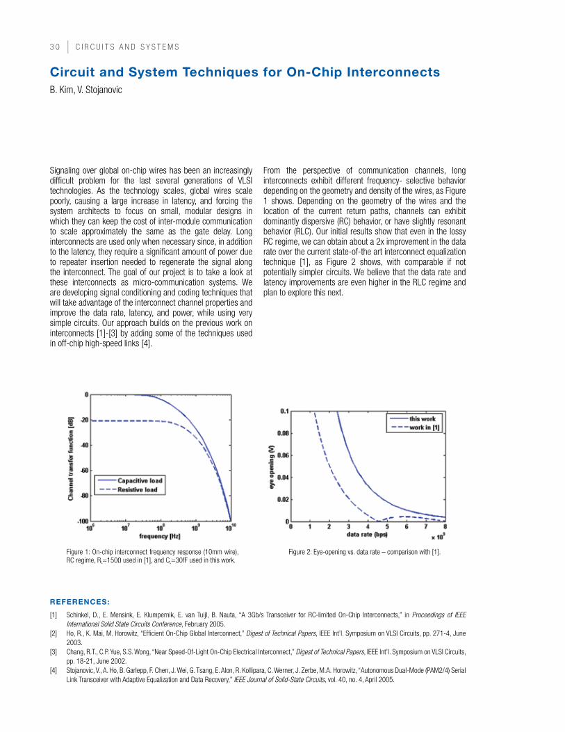
From the perspective of communication channels, long interconnects exhibit different frequency- selective behavior depending on the geometry and density of the wires, as Figure 1 shows. Depending on the geometry of the wires and the location of the current return paths, channels can exhibit dominantly dispersive (RC) behavior, or have slightly resonant behavior (RLC). Our initial results show that even in the lossy RC regime, we can obtain about a 2x improvement in the data rate over the current state-of-the art interconnect equalization technique [1], as Figure 2 shows, with comparable if not potentially simpler circuits. We believe that the data rate and latency improvements are even higher in the RLC regime and plan to explore this next.
Figure 1: On-chip interconnect frequency response (10mm wire), RC regime, RL=150Ω used in [1], and CL=30fF used in this work.
Figure 2: Eye-opening vs. data rate – comparison with [1].
REFEREncEs:
[1] Schinkel, D., E. Mensink, E. Klumpernik, E. van Tuijl, B. Nauta, “A 3Gb/s Transceiver for RC-limited On-Chip Interconnects,” in Proceedings of IEEE International Solid State Circuits Conference, February 2005.
[2] Ho, R., K. Mai, M. Horowitz, “Efficient On-Chip Global Interconnect,” Digest of Technical Papers, IEEE Int’l. Symposium on VLSI Circuits, pp. 271-4, June 2003.
[3] Chang, R.T., C.P. Yue, S.S. Wong, “Near Speed-Of-Light On-Chip Electrical Interconnect,” Digest of Technical Papers, IEEE Int’l. Symposium on VLSI Circuits, pp. 18-21, June 2002.
[4] Stojanovic, V., A. Ho, B. Garlepp, F. Chen, J. Wei, G. Tsang, E. Alon, R. Kollipara, C. Werner, J. Zerbe, M.A. Horowitz, “Autonomous Dual-Mode (PAM2/4) Serial Link Transceiver with Adaptive Equalization and Data Recovery,” IEEE Journal of Solid-State Circuits, vol. 40, no. 4, April 2005.
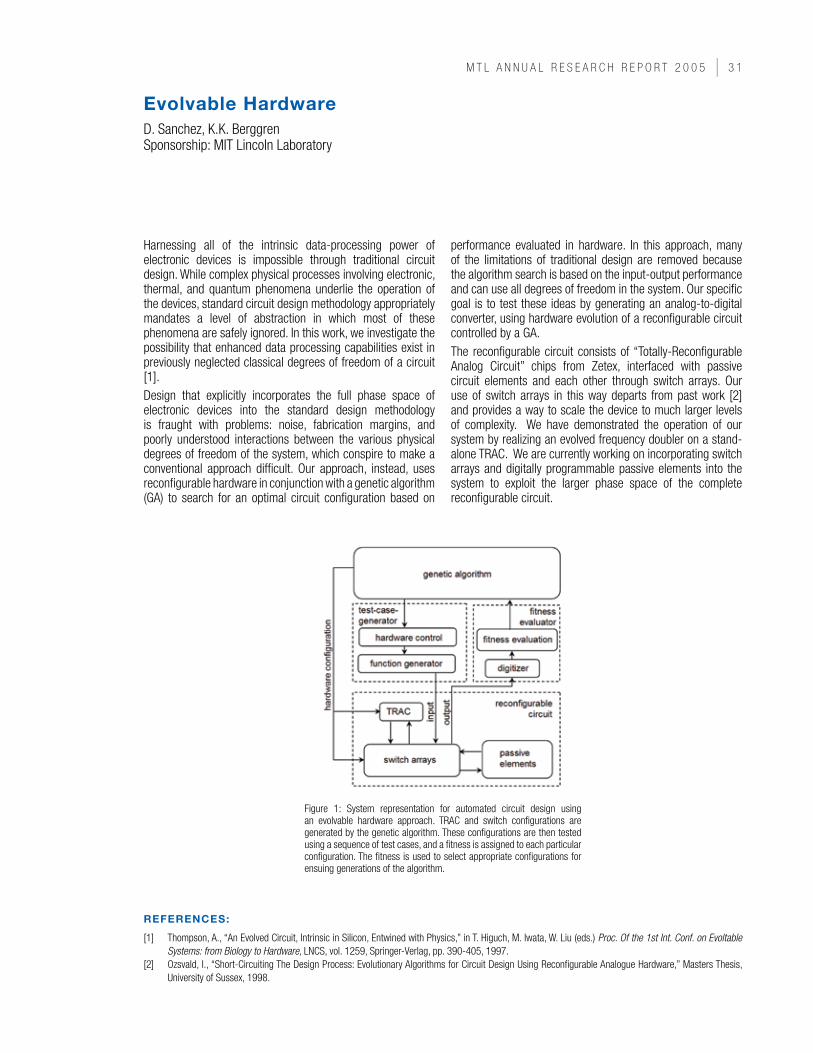
m t L a n n u a L r e s e a r C H r e P O r t 0 0 5 | 1
Evolvable HardwareD. Sanchez, K.K. Berggren Sponsorship: MIT Lincoln Laboratory
Harnessing all of the intrinsic data-processing power of electronic devices is impossible through traditional circuit design. While complex physical processes involving electronic, thermal, and quantum phenomena underlie the operation of the devices, standard circuit design methodology appropriately mandates a level of abstraction in which most of these phenomena are safely ignored. In this work, we investigate the possibility that enhanced data processing capabilities exist in previously neglected classical degrees of freedom of a circuit [1]. Design that explicitly incorporates the full phase space of electronic devices into the standard design methodology is fraught with problems: noise, fabrication margins, and poorly understood interactions between the various physical degrees of freedom of the system, which conspire to make a conventional approach difficult. Our approach, instead, uses reconfigurable hardware in conjunction with a genetic algorithm (GA) to search for an optimal circuit configuration based on
performance evaluated in hardware. In this approach, many of the limitations of traditional design are removed because the algorithm search is based on the input-output performance and can use all degrees of freedom in the system. Our specific goal is to test these ideas by generating an analog-to-digital converter, using hardware evolution of a reconfigurable circuit controlled by a GA. The reconfigurable circuit consists of “Totally-Reconfigurable Analog Circuit” chips from Zetex, interfaced with passive circuit elements and each other through switch arrays. Our use of switch arrays in this way departs from past work [2] and provides a way to scale the device to much larger levels of complexity. We have demonstrated the operation of our system by realizing an evolved frequency doubler on a stand-alone TRAC. We are currently working on incorporating switch arrays and digitally programmable passive elements into the system to exploit the larger phase space of the complete reconfigurable circuit.
Figure 1: System representation for automated circuit design using an evolvable hardware approach. TRAC and switch configurations are generated by the genetic algorithm. These configurations are then tested using a sequence of test cases, and a fitness is assigned to each particular configuration. The fitness is used to select appropriate configurations for ensuing generations of the algorithm.
REFEREncEs:
[1] Thompson, A., “An Evolved Circuit, Intrinsic in Silicon, Entwined with Physics,” in T. Higuch, M. Iwata, W. Liu (eds.) Proc. Of the 1st Int. Conf. on Evoltable Systems: from Biology to Hardware, LNCS, vol. 1259, Springer-Verlag, pp. 390-405, 1997.
[2] Ozsvald, I., “Short-Circuiting The Design Process: Evolutionary Algorithms for Circuit Design Using Reconfigurable Analogue Hardware,” Masters Thesis, University of Sussex, 1998.
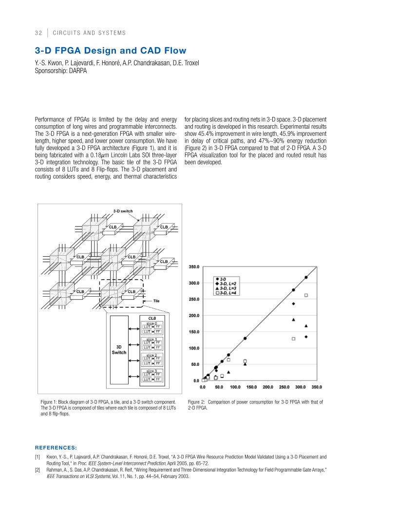
| C i r C u i t s a n d s y s t e m s
3-D FPGA Design and cAD FlowY.-S. Kwon, P. Lajevardi, F. Honoré, A.P. Chandrakasan, D.E. Troxel Sponsorship: DARPA
Performance of FPGAs is limited by the delay and energy consumption of long wires and programmable interconnects. The 3-D FPGA is a next-generation FPGA with smaller wire-length, higher speed, and lower power consumption. We have fully developed a 3-D FPGA architecture (Figure 1), and it is being fabricated with a 0.18µm Lincoln Labs SOI three-layer 3-D integration technology. The basic tile of the 3-D FPGA consists of 8 LUTs and 8 Flip-flops. The 3-D placement and routing considers speed, energy, and thermal characteristics
for placing slices and routing nets in 3-D space. 3-D placement and routing is developed in this research. Experimental results show 45.4% improvement in wire length, 45.9% improvement in delay of critical paths, and 47%~90% energy reduction (Figure 2) in 3-D FPGA compared to that of 2-D FPGA. A 3-D FPGA visualization tool for the placed and routed result has been developed.
Figure 1: Block diagram of 3-D FPGA, a tile, and a 3-D switch component. The 3-D FPGA is composed of tiles where each tile is composed of 8 LUTs and 8 flip-flops.
Figure 2: Comparison of power consumption for 3-D FPGA with that of 2-D FPGA.
REFEREncEs:
[1] Kwon, Y.-S., P. Lajevardi, A.P. Chandrakasan, F. Honoré, D.E. Troxel, “A 3-D FPGA Wire Resource Prediction Model Validated Using a 3-D Placement and Routing Tool,“ in Proc. IEEE System-Level Interconnect Prediction, April 2005, pp. 65-72.
[2] Rahman, A., S. Das, A.P. Chandrakasan, R. Reif, “Wiring Requirement and Three-Dimensional Integration Technology for Field Programmable Gate Arrays,” IEEE Transactions on VLSI Systems, Vol. 11, No. 1, pp. 44–54, February 2003.

m t L a n n u a L r e s e a r C H r e P O r t 0 0 5 |
Low-Power FPGA circuits and cADF. Honoré, A.P. Chandrakasan Sponsorship: MARCO IFC
Reconfigurability is becoming an important factor in the design of systems. FPGAs are extending their application area from system prototyping to custom application implementation but they are much slower and less power-efficient than ASIC systems. We have developed a power- and performance-scalable multi-VDD FPGA. The interconnect overhead for FPGA’s is a large fraction of the power and delay, due to the use of programmable switch elements. Fine-grain voltage domains allow low-energy operation in non-critical areas of logic and routing segments. A modified, programmable switch architecture allows long paths to be pipelined to meet critical path timing or, alternatively, allow reduced voltage operation with minimal performance impact. A better partitioning of non-critical configuration elements to reduce wire lengths produces further reduction in interconnect capacitance. Approximately 70% reduction in the array area is achieved by relocating the switch block and CLB configuration memory to the periphery of the array, resulting in reduced parasitic capacitance on the critical routing wires.
A power-aware place-and-route tool determines which non-critical paths can run at reduced voltage and configures the various domains of the array accordingly. Thus, selecting the appropriate choice of supply voltage for each domain achieves an average 52% improvement in power for the same performance (Figure 1). Low-overhead level converters provide voltage conversion between domains. With these fine-grain controls, the software can make tradeoffs between power and performance and deliver maximum power savings with minimum performance impact. Sub-threshold leakage reduction is also achieved with fine-grain sleep regions that shut down the power supply to inactive circuits. We have designed a 3x3mm chip (Figure 2) using a customized ASIC flow to validate the approach and have developed custom CAD tools to automate the implementation of some of these techniques.The chip was fabricated in 0.18µm CMOS technology. We acknowledge National Semiconductor for providing the fabrication services.
Figure 1: Benchmark results showing an average improvement of 52% at a VDDH of 1.8V and VDDL of 0.9V.
Figure 2: Layout of one logic and switch block tile.
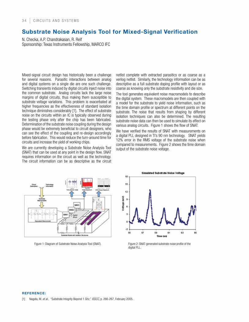
| C i r C u i t s a n d s y s t e m s
substrate noise Analysis Tool for Mixed-signal VerificationN. Checka, A.P. Chandrakasan, R. Reif Sponsorship: Texas Instruments Fellowship, MARCO IFC
Mixed-signal circuit design has historically been a challenge for several reasons. Parasitic interactions between analog and digital systems on a single die are one such challenge. Switching transients induced by digital circuits inject noise into the common substrate. Analog circuits lack the large noise margins of digital circuits, thus making them susceptible to substrate voltage variations. This problem is exacerbated at higher frequencies as the effectiveness of standard isolation technique diminishes considerably [1]. The effect of substrate noise on the circuits within an IC is typically observed during the testing phase only after the chip has been fabricated. Determination of the substrate noise coupling during the design phase would be extremely beneficial to circuit designers, who can see the effect of the coupling and re-design accordingly before fabrication. This would reduce the turn-around time for circuits and increase the yield of working chips.We are currently developing a Substrate Noise Analysis Tool (SNAT) that can be used at any point in the design flow. SNAT requires information on the circuit as well as the technology. The circuit information can be as descriptive as the circuit
netlist complete with extracted parasitics or as coarse as a verilog netlist. Similarly, the technology information can be as descriptive as a full substrate doping profile with layout or as coarse as knowing only the substrate resistivity and die size.The tool generates equivalent noise macromodels to describe the digital system. These macromodels are then coupled with a model for the substrate to yield noise information, such as the time domain profile or spectrum at different points on the substrate. The noise that results from shaping by different isolation techniques can also be determined. The resulting substrate noise data can then be used to simulate its effect on various analog circuits. Figure 1 shows the flow of SNAT.We have verified the results of SNAT with measurements on a digital PLL designed in TI’s 90 nm technology. SNAT yields 12% error in the RMS voltage of the substrate noise when compared to measurements. Figure 2 shows the time domain output of the substrate noise voltage.
Figure 1: Diagram of Substrate Noise Analysis Tool (SNAT). Figure 2: SNAT-generated substrate noise profile of the digital PLL.
REFEREncE:
[1] Nagata, M. et al., “Substrate Integrity Beyond 1 Ghz,” ISSCC, p. 266-267, February 2005.
m t L a n n u a L r e s e a r C H r e P O r t 0 0 5 | 5
convex Optimization-Aided Design of Analog and Mixed-signal communication systemsR. Sredojevic, V. Stojanovic, J.L. Dawson
Many integrated communication systems today are constrained by either throughput or power dissipation. Cases from high-speed I/O interfaces in processors and routers to low-power radios in cell phones and sensors force designers to tackle one of the two dual problems – optimizing the overall data rate with given power constraints or minimizing the power for given throughput. While much work has gone into both the circuit and communications sides of the problem, the hardest part seems to be communicating the requirements/costs and characteristics of circuits and components to the algorithm level and vice versa, so that the overall optimum can occur. Many design hours and iterations on the system architectures are needed before a system is designed, and even then, very little data exists on the scope of design space or the cost/performance space of the implemented components. What is the new optimal system if the specifications change slightly? To solve these problems, we intend to use the convex optimization as a framework to connect the circuit and system design abstractions.We are developing a design-optimization framework in which an integrated communication system is constructed out of pre-characterized macros of analog, digital, and mixed-signal circuits. Through the use of convex optimization, tradeoff functions and defined regions of operation are found for each macro. This information is then used at a higher–system design level to determine the right blend of algorithms and
system architecture that implement a globally efficient communication system. Convex optimization is critical to this effort, since it also provides the sensitivities of each objective function of the underlying circuit/block parameters, which builds intuition about the design and guides the designer in making intelligent topology changes. This challenging work is currently considered akin to black magic, since the problem, in general, is combinatorial and NP-hard.We intend to follow the Barcelona Design work [1]-[3] by putting their effort into a more general framework. We will use the MuseTM optimization language developed by Barcelona Design (made available to universities) to integrate the convex optimization framework in the IC design flow. Doing so will allow us not only to optimize a given circuit architecture, but also to explore different architectures, finding the ones that lend themselves nicely to convex optimization. We are currently working on a library of these adjustable or optimizable macros, such as mixers, VCOs, amplifiers, ADCs, DACs, and even their building elements. With this base and initial optimization results for each of the macros, we intend to engage in a system-level optimization on two example systems: a narrowband communication system (for example, a cell phone radio or a sensor) and a wideband communication system (an ultra-wideband radio or a multi-Gb/s high-speed chip-to-chip link [4],[5]).
REFEREncEs:
[1] Hershenson, M.M., “Efficient Description of the Design Space of Analog Circuits,” Design Automation Conference, 2003. [2] Hershenson, M.M., “Design of Pipeline Analog-To-Digital Converters via Geometric Programming,” ICCAD 2002. [3] Colleran, D.M. et al.,“Optimization of Phase-Locked Loop Circuits via Geometric Programming,” IEEE Custom Integrated Circuits Conference, 2003. [4] Stojanovic, V., A. Amirkhany, M. Horowitz, “Optimal Linear Precoding with Theoretical and Practical Data Rates in High-Speed Serial-Link Backplane
Communication,” IEEE International Conference on Communications, June 2004. [5] Stojanovic, V., A. Ho, B. Garlepp, F. Chen, J. Wei, E. Alon, C. Werner, J. Zerbe, M.A. Horowitz, “Adaptive Equalization and Data Recovery in a Dual-Mode
(PAM2/4) Serial Link Transceiver,” IEEE Symposium on VLSI Circuits, June 2004, pp. 348-351.
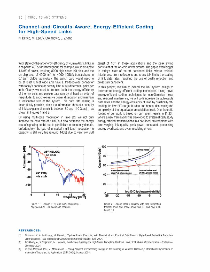
| C i r C u i t s a n d s y s t e m s
channel-and-circuits-Aware, Energy-Efficient coding for High-speed LinksN. Blitvic, M. Lee, V. Stojanovic, L. Zheng
With state-of-the-art energy-efficiency of 40mW/Gb/s, links in a chip with 40Tb/s I/O throughput, for example, would dissipate 1.6kW of power, requiring 8000 high-speed I/O pins, and the on-chip area of 4000mm2 for 4000 10Gb/s transceivers, in 0.13µm CMOS technology. The switch card would need to be at least 8 feet wide and have a 13-feet-wide connector with today’s connector density limit of 50 differential pairs per inch. Clearly, we need to improve both the energy-efficiency of the link cells and per/pin data rate by at least an order of magnitude, to avoid excessive power dissipation and maintain a reasonable size of the system. This data rate scaling is theoretically possible, since the information theoretic capacity of link backplane channels is between 80 and 110 Gb/s [1], as shown in Figures 1 and 2.By using multi-tone modulation in links [2], we not only increase the data rate of a link, but also decrease the energy cost of signaling per bit due to parallelism in frequency domain. Unfortunately, the gap of uncoded multi-tone modulation to capacity is still very big (around 14dB) due to very low BER
target of 10-15 in these applications and the peak swing constraint of the on-chip driver circuits. The gap is even bigger in today’s state-of-the-art baseband links, where residual interference from reflections and cross-talk limits the scaling of link data rates, requiring the use of costly reflection and cross-talk cancellers.In this project, we aim to extend the link system design to incorporate energy-efficient coding techniques. Using novel energy-efficient coding techniques for non-Gaussian noise and residual interference, we will both increase the achievable data rates and the energy-efficiency of links by drastically off-loading the low-BER target burden and hence, decreasing the complexity of the equalization/modulation level. One theoretic footing of our work is based on our recent results in [1],[3], where a new framework was developed to systematically study energy efficient transmissions in a non-ideal environment, with time-varying link quality, peak-power constraint, processing energy overhead, and even, modeling errors.
Figure 1: Legacy (FR4) and new, microwave-engineered (NELCO) backplane channels.
Figure 2: Legacy channel capacity with 50Ω termination thermal noise and phase noise from LC and ring VCO-based PLL.
REFEREncEs:
[1] Stojanovic, V., A. Amirkhany, M. Horowitz, “Optimal Linear Precoding with Theoretical and Practical Data Rates in High-Speed Serial-Link Backplane Communication,” IEEE International Conference on Communications, June 2004.
[2] Amirkhany, A., V. Stojanovic, M. Horowitz, “Multi-Tone Signaling for High-Speed Backplane Electrical Links,” IEEE Global Communications Conference, December 2004.
[3] Youssef-Massaad, P.G., M. Médard and L. Zheng, “Impact of Processing Energy on the Capacity of Wireless Channels,” International Symposium on Information Theory and its Applications (ISITA 2004), October 2004.
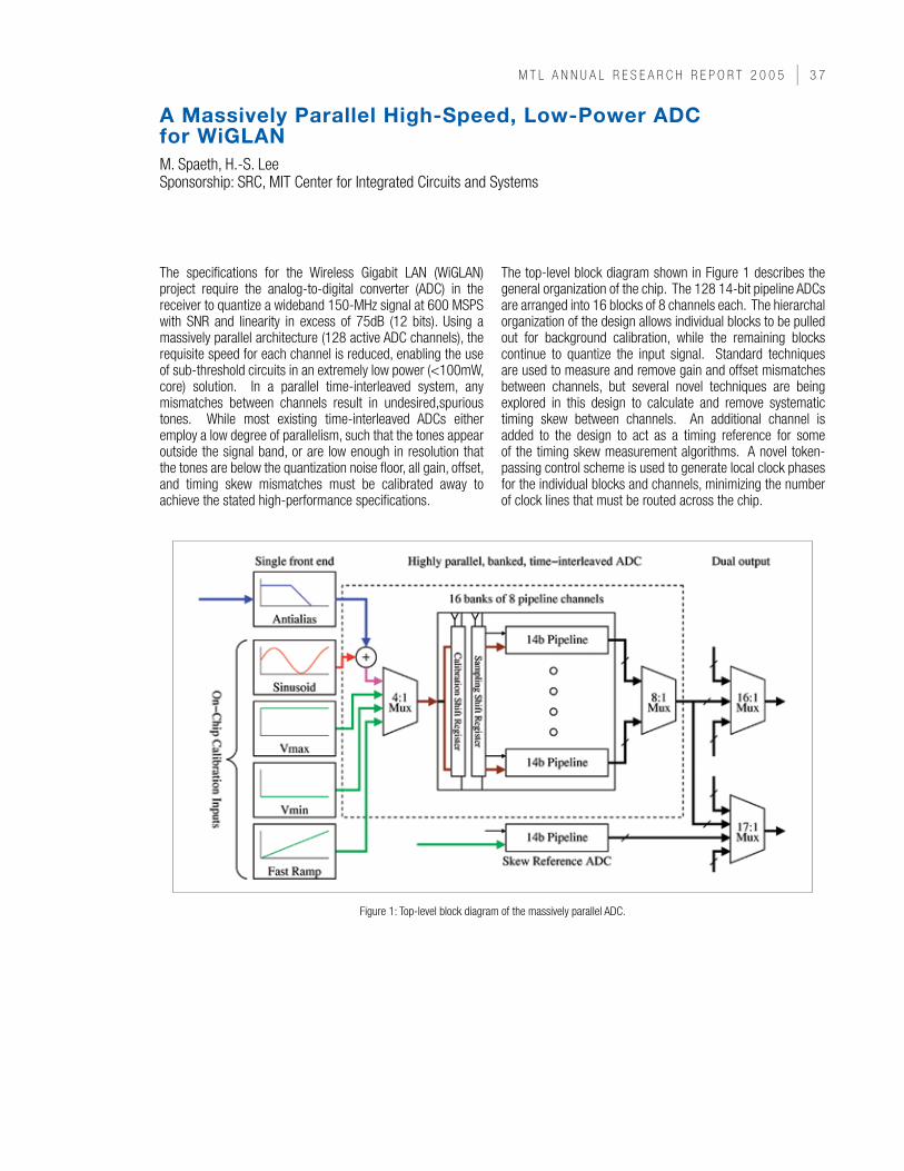
m t L a n n u a L r e s e a r C H r e P O r t 0 0 5 |
A Massively Parallel High-speed, Low-Power ADc for WiGLAnM. Spaeth, H.-S. Lee Sponsorship: SRC, MIT Center for Integrated Circuits and Systems
The specifications for the Wireless Gigabit LAN (WiGLAN) project require the analog-to-digital converter (ADC) in the receiver to quantize a wideband 150-MHz signal at 600 MSPS with SNR and linearity in excess of 75dB (12 bits). Using a massively parallel architecture (128 active ADC channels), the requisite speed for each channel is reduced, enabling the use of sub-threshold circuits in an extremely low power (<100mW, core) solution. In a parallel time-interleaved system, any mismatches between channels result in undesired,spurious tones. While most existing time-interleaved ADCs either employ a low degree of parallelism, such that the tones appear outside the signal band, or are low enough in resolution that the tones are below the quantization noise floor, all gain, offset, and timing skew mismatches must be calibrated away to achieve the stated high-performance specifications.
The top-level block diagram shown in Figure 1 describes the general organization of the chip. The 128 14-bit pipeline ADCs are arranged into 16 blocks of 8 channels each. The hierarchal organization of the design allows individual blocks to be pulled out for background calibration, while the remaining blocks continue to quantize the input signal. Standard techniques are used to measure and remove gain and offset mismatches between channels, but several novel techniques are being explored in this design to calculate and remove systematic timing skew between channels. An additional channel is added to the design to act as a timing reference for some of the timing skew measurement algorithms. A novel token-passing control scheme is used to generate local clock phases for the individual blocks and channels, minimizing the number of clock lines that must be routed across the chip.
Figure 1: Top-level block diagram of the massively parallel ADC.

| C i r C u i t s a n d s y s t e m s
Background self-calibration of A/D converters by Direct Transition Point AlignmentL. Brooks, H.-S. Lee, G. Wornell Sponsorship: MIT Center for Integrated Circuits and Systems
Traditional calibration methods for A/D converters employ either foreground or background calibration. The foreground calibration requires a separate calibration phase during which regular conversion must be halted. Often, the converter must be recalibrated due to the drift of the converter characteristic. Each recalibration requires discontinuing the regular conversion until the calibration is complete. The background calibration circumvents these issues by continuously calibrating the converter in the background while the converter is working normally. However, in order to accommodate background calibration, typically redundant channels or stages of converters are required so that the extra channel/stage can be replaced for those that are being calibrated. A slow, but accurate, “reference” ADC is often employed to calibrate the fast converter against. Some techniques employ special input signals, such as the reference voltage and/or ground for the calibration. Alternately, some background calibration methods use a “skip-and-fill” technique, in which normal conversion samples are skipped and filled by digital interpolation. During the skipped samples, calibration is performed. Such calibration requires a complicated interpolation algorithm to fill the missing data as well as to reduce the input signal bandwidth. In this research, we are developing a novel background digital self-calibration method applicable to any A/D converter topology. The only requirement is that the raw A/D converter must be free of ”wide” codes that cannot be removed by digital calibration alone. This condition is necessary for any fully digital calibration. The absence of wide codes can be easily guaranteed, either by introducing over-range capability or intentionally reducing the inter-stage gain. The background calibration in this research requires neither redundant channels for calibrating off-line nor special input signal, such as the reference voltage or ground. Instead, the errors are calibrated directly from the digital output statistics from regular input signals.
The advantages of the new direct calibration method are numerous. There is no need for either additional analog hardware, such as a redundant channels or stages of the converter, or a “reference” converter to calibrate against. The calibration is highly accurate because the transition points are directly aligned. Also, since the calibration is performed from regular input signals, no special signals are necessary for calibration. The behavioral simulation indicates calibration to a very high accuracy is feasible. Presently, we are working on a detailed system design using the new comparator-based switched capacitor (CBSC) concept.
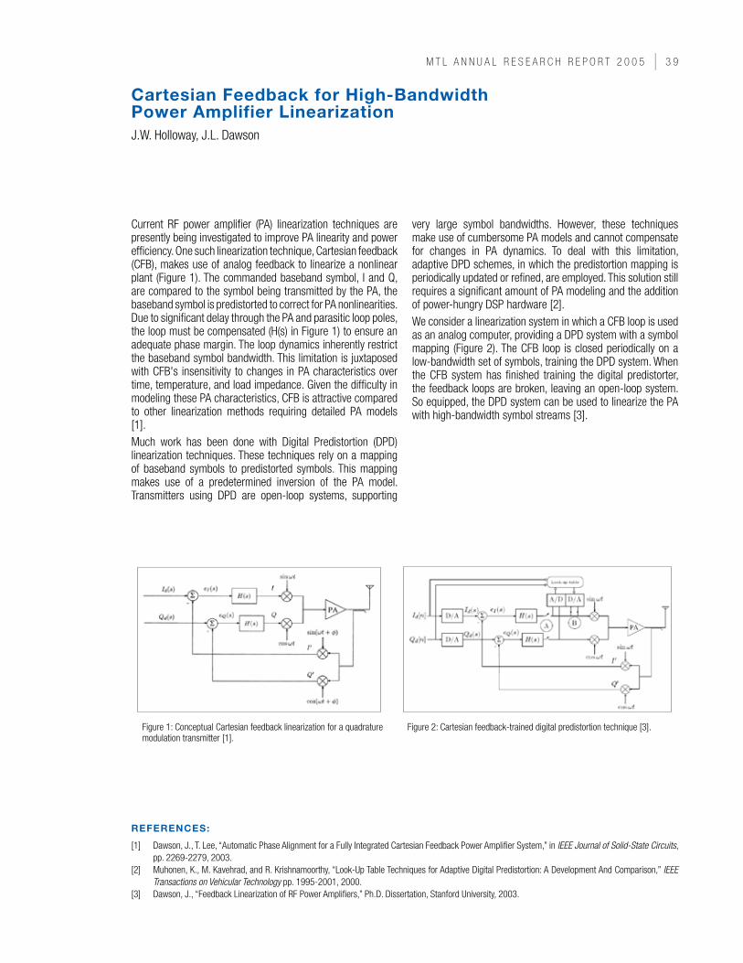
m t L a n n u a L r e s e a r C H r e P O r t 0 0 5 |
cartesian Feedback for High-Bandwidth Power Amplifier LinearizationJ.W. Holloway, J.L. Dawson
Current RF power amplifier (PA) linearization techniques are presently being investigated to improve PA linearity and power efficiency. One such linearization technique, Cartesian feedback (CFB), makes use of analog feedback to linearize a nonlinear plant (Figure 1). The commanded baseband symbol, I and Q, are compared to the symbol being transmitted by the PA, the baseband symbol is predistorted to correct for PA nonlinearities. Due to significant delay through the PA and parasitic loop poles, the loop must be compensated (H(s) in Figure 1) to ensure an adequate phase margin. The loop dynamics inherently restrict the baseband symbol bandwidth. This limitation is juxtaposed with CFB's insensitivity to changes in PA characteristics over time, temperature, and load impedance. Given the difficulty in modeling these PA characteristics, CFB is attractive compared to other linearization methods requiring detailed PA models [1].Much work has been done with Digital Predistortion (DPD) linearization techniques. These techniques rely on a mapping of baseband symbols to predistorted symbols. This mapping makes use of a predetermined inversion of the PA model. Transmitters using DPD are open-loop systems, supporting
very large symbol bandwidths. However, these techniques make use of cumbersome PA models and cannot compensate for changes in PA dynamics. To deal with this limitation, adaptive DPD schemes, in which the predistortion mapping is periodically updated or refined, are employed. This solution still requires a significant amount of PA modeling and the addition of power-hungry DSP hardware [2].We consider a linearization system in which a CFB loop is used as an analog computer, providing a DPD system with a symbol mapping (Figure 2). The CFB loop is closed periodically on a low-bandwidth set of symbols, training the DPD system. When the CFB system has finished training the digital predistorter, the feedback loops are broken, leaving an open-loop system. So equipped, the DPD system can be used to linearize the PA with high-bandwidth symbol streams [3].
Figure 1: Conceptual Cartesian feedback linearization for a quadrature modulation transmitter [1].
Figure 2: Cartesian feedback-trained digital predistortion technique [3].
REFEREncEs:
[1] Dawson, J., T. Lee, “Automatic Phase Alignment for a Fully Integrated Cartesian Feedback Power Amplifier System,” in IEEE Journal of Solid-State Circuits, pp. 2269-2279, 2003.
[2] Muhonen, K., M. Kavehrad, and R. Krishnamoorthy, “Look-Up Table Techniques for Adaptive Digital Predistortion: A Development And Comparison,” IEEE Transactions on Vehicular Technology pp. 1995-2001, 2000.
[3] Dawson, J., “Feedback Linearization of RF Power Amplifiers,” Ph.D. Dissertation, Stanford University, 2003.
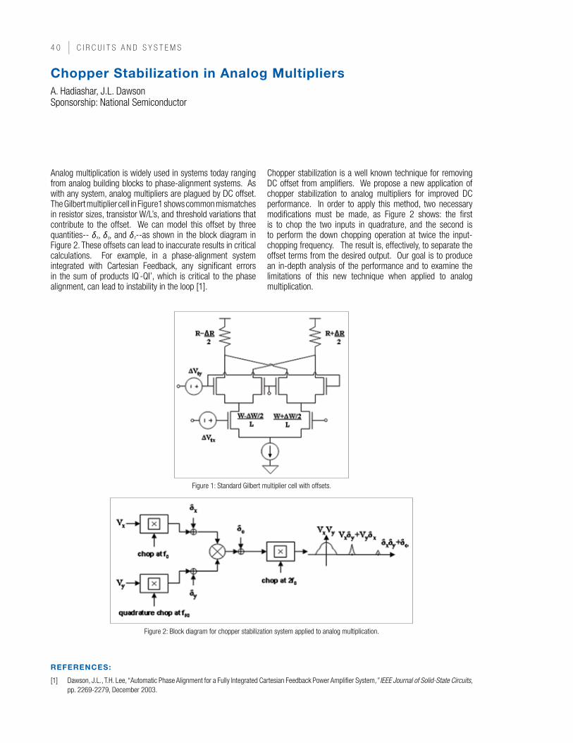
0 | C i r C u i t s a n d s y s t e m s
chopper stabilization in Analog MultipliersA. Hadiashar, J.L. Dawson Sponsorship: National Semiconductor
Analog multiplication is widely used in systems today ranging from analog building blocks to phase-alignment systems. As with any system, analog multipliers are plagued by DC offset. The Gilbert multiplier cell in Figure1 shows common mismatches in resistor sizes, transistor W/L’s, and threshold variations that contribute to the offset. We can model this offset by three quantities-- δx, δy, and δz--as shown in the block diagram in Figure 2. These offsets can lead to inaccurate results in critical calculations. For example, in a phase-alignment system integrated with Cartesian Feedback, any significant errors in the sum of products IQ’-QI’, which is critical to the phase alignment, can lead to instability in the loop [1].
Chopper stabilization is a well known technique for removing DC offset from amplifiers. We propose a new application of chopper stabilization to analog multipliers for improved DC performance. In order to apply this method, two necessary modifications must be made, as Figure 2 shows: the first is to chop the two inputs in quadrature, and the second is to perform the down chopping operation at twice the input-chopping frequency. The result is, effectively, to separate the offset terms from the desired output. Our goal is to produce an in-depth analysis of the performance and to examine the limitations of this new technique when applied to analog multiplication.
REFEREncEs:
[1] Dawson, J.L., T.H. Lee, “Automatic Phase Alignment for a Fully Integrated Cartesian Feedback Power Amplifier System,” IEEE Journal of Solid-State Circuits, pp. 2269-2279, December 2003.
Figure 1: Standard Gilbert multiplier cell with offsets.
Figure 2: Block diagram for chopper stabilization system applied to analog multiplication.
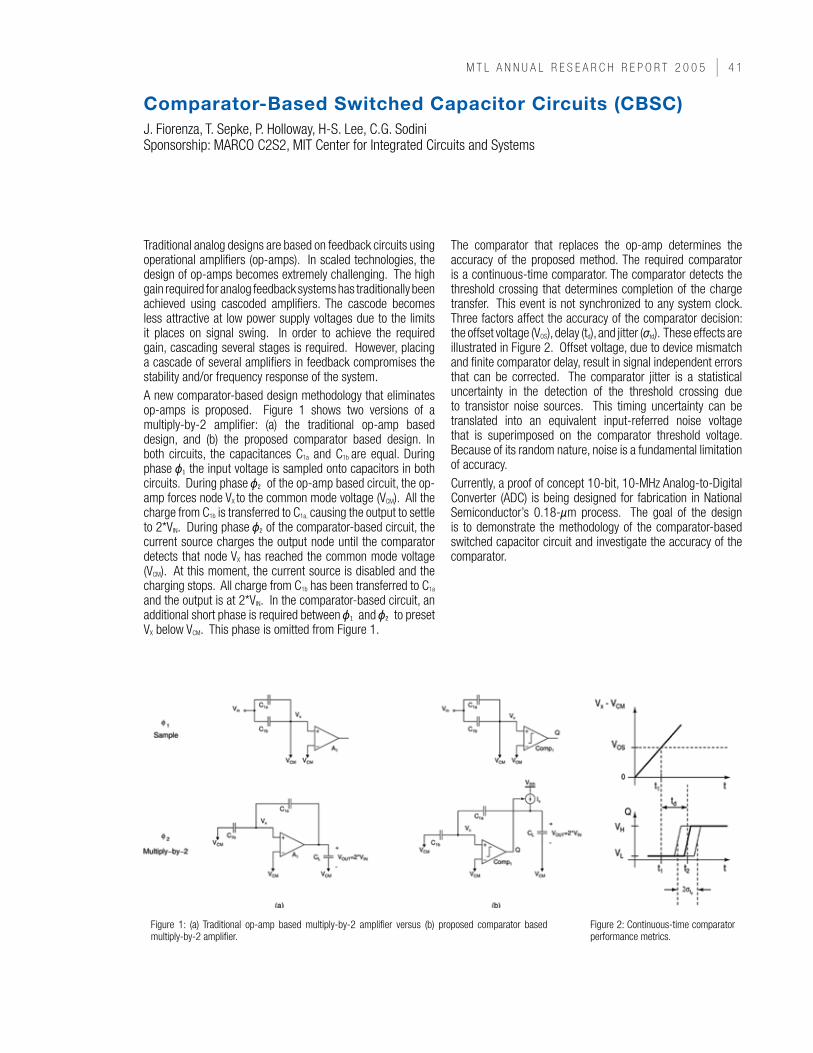
m t L a n n u a L r e s e a r C H r e P O r t 0 0 5 | 1
comparator-Based switched capacitor circuits (cBsc)J. Fiorenza, T. Sepke, P. Holloway, H-S. Lee, C.G. Sodini Sponsorship: MARCO C2S2, MIT Center for Integrated Circuits and Systems
Traditional analog designs are based on feedback circuits using operational amplifiers (op-amps). In scaled technologies, the design of op-amps becomes extremely challenging. The high gain required for analog feedback systems has traditionally been achieved using cascoded amplifiers. The cascode becomes less attractive at low power supply voltages due to the limits it places on signal swing. In order to achieve the required gain, cascading several stages is required. However, placing a cascade of several amplifiers in feedback compromises the stability and/or frequency response of the system. A new comparator-based design methodology that eliminates op-amps is proposed. Figure 1 shows two versions of a multiply-by-2 amplifier: (a) the traditional op-amp based design, and (b) the proposed comparator based design. In both circuits, the capacitances C1a and C1b are equal. During phase φ1 the input voltage is sampled onto capacitors in both circuits. During phase φ2 of the op-amp based circuit, the op-amp forces node VX to the common mode voltage (VCM). All the charge from C1b is transferred to C1a, causing the output to settle to 2*VIN. During phase φ2 of the comparator-based circuit, the current source charges the output node until the comparator detects that node VX has reached the common mode voltage (VCM). At this moment, the current source is disabled and the charging stops. All charge from C1b has been transferred to C1a and the output is at 2*VIN. In the comparator-based circuit, an additional short phase is required between φ1 and φ2 to preset VX below VCM. This phase is omitted from Figure 1.
The comparator that replaces the op-amp determines the accuracy of the proposed method. The required comparator is a continuous-time comparator. The comparator detects the threshold crossing that determines completion of the charge transfer. This event is not synchronized to any system clock. Three factors affect the accuracy of the comparator decision: the offset voltage (VOS), delay (td), and jitter (σtd). These effects are illustrated in Figure 2. Offset voltage, due to device mismatch and finite comparator delay, result in signal independent errors that can be corrected. The comparator jitter is a statistical uncertainty in the detection of the threshold crossing due to transistor noise sources. This timing uncertainty can be translated into an equivalent input-referred noise voltage that is superimposed on the comparator threshold voltage. Because of its random nature, noise is a fundamental limitation of accuracy.Currently, a proof of concept 10-bit, 10-MHz Analog-to-Digital Converter (ADC) is being designed for fabrication in National Semiconductor’s 0.18-µm process. The goal of the design is to demonstrate the methodology of the comparator-based switched capacitor circuit and investigate the accuracy of the comparator.
Figure 1: (a) Traditional op-amp based multiply-by-2 amplifier versus (b) proposed comparator based multiply-by-2 amplifier.
Figure 2: Continuous-time comparator performance metrics.
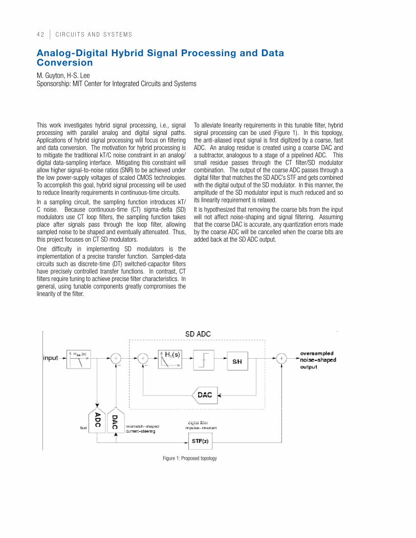
| C i r C u i t s a n d s y s t e m s
Analog-Digital Hybrid signal Processing and Data conversionM. Guyton, H-S. Lee Sponsorship: MIT Center for Integrated Circuits and Systems
This work investigates hybrid signal processing, i.e., signal processing with parallel analog and digital signal paths. Applications of hybrid signal processing will focus on filtering and data conversion. The motivation for hybrid processing is to mitigate the traditional kT/C noise constraint in an analog/digital data-sampling interface. Mitigating this constraint will allow higher signal-to-noise ratios (SNR) to be achieved under the low power-supply voltages of scaled CMOS technologies. To accomplish this goal, hybrid signal processing will be used to reduce linearity requirements in continuous-time circuits.In a sampling circuit, the sampling function introduces kT/C noise. Because continuous-time (CT) sigma-delta (SD) modulators use CT loop filters, the sampling function takes place after signals pass through the loop filter, allowing sampled noise to be shaped and eventually attenuated. Thus, this project focuses on CT SD modulators. One difficulty in implementing SD modulators is the implementation of a precise transfer function. Sampled-data circuits such as discrete-time (DT) switched-capacitor filters have precisely controlled transfer functions. In contrast, CT filters require tuning to achieve precise filter characteristics. In general, using tunable components greatly compromises the linearity of the filter.
To alleviate linearity requirements in this tunable filter, hybrid signal processing can be used (Figure 1). In this topology, the anti-aliased input signal is first digitized by a coarse, fast ADC. An analog residue is created using a coarse DAC and a subtractor, analogous to a stage of a pipelined ADC. This small residue passes through the CT filter/SD modulator combination. The output of the coarse ADC passes through a digital filter that matches the SD ADC’s STF and gets combined with the digital output of the SD modulator. In this manner, the amplitude of the SD modulator input is much reduced and so its linearity requirement is relaxed. It is hypothesized that removing the coarse bits from the input will not affect noise-shaping and signal filtering. Assuming that the coarse DAC is accurate, any quantization errors made by the coarse ADC will be cancelled when the coarse bits are added back at the SD ADC output.
Figure 1: Proposed topology
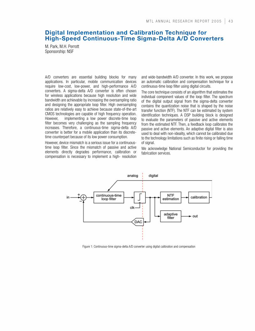
m t L a n n u a L r e s e a r C H r e P O r t 0 0 5 |
Digital Implementation and calibration Technique for High-speed continuous-Time sigma-Delta A/D convertersM. Park, M.H. Perrott Sponsorship: NSF
A/D converters are essential building blocks for many applications. In particular, mobile communication devices require low-cost, low-power, and high-performance A/D converters. A sigma-delta A/D converter is often chosen for wireless applications because high resolution and wide bandwidth are achievable by increasing the oversampling ratio and designing the appropriate loop filter. High oversampling ratios are relatively easy to achieve because state-of-the-art CMOS technologies are capable of high frequency operation. However, implementing a low power discrete-time loop filter becomes very challenging as the sampling frequency increases. Therefore, a continuous-time sigma-delta A/D converter is better for a mobile application than its discrete-time counterpart because of its low power consumption.However, device mismatch is a serious issue for a continuous-time loop filter. Since the mismatch of passive and active elements directly degrades performance, calibration or compensation is necessary to implement a high- resolution
and wide-bandwidth A/D converter. In this work, we propose an automatic calibration and compensation technique for a continuous-time loop filter using digital circuits.The core technique consists of an algorithm that estimates the individual component values of the loop filter. The spectrum of the digital output signal from the sigma-delta converter contains the quantization noise that is shaped by the noise transfer function (NTF). The NTF can be estimated by system identification techniques. A DSP building block is designed to evaluate the parameters of passive and active elements from the estimated NTF. Then, a feedback loop calibrates the passive and active elements. An adaptive digital filter is also used to deal with non-ideality, which cannot be calibrated due to the technology limitations such as finite rising or falling time of signal.We acknowledge National Semiconductor for providing the fabrication services.
Figure 1: Continuous-time sigma-delta A/D converter using digital calibration and compensation
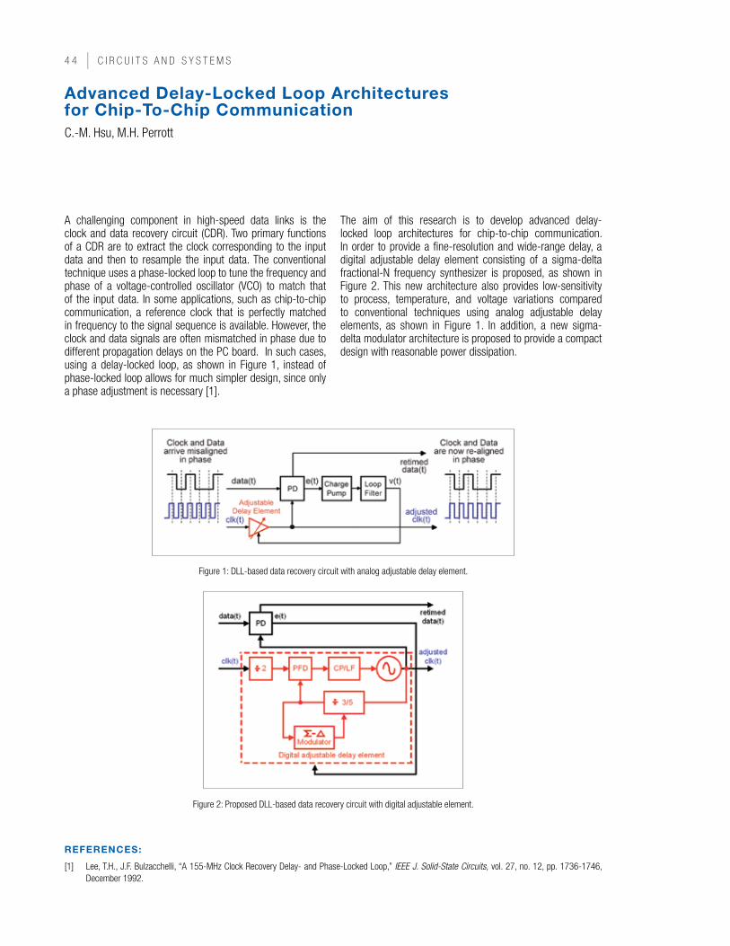
| C i r C u i t s a n d s y s t e m s
Advanced Delay-Locked Loop Architectures for chip-To-chip communicationC.-M. Hsu, M.H. Perrott
A challenging component in high-speed data links is the clock and data recovery circuit (CDR). Two primary functions of a CDR are to extract the clock corresponding to the input data and then to resample the input data. The conventional technique uses a phase-locked loop to tune the frequency and phase of a voltage-controlled oscillator (VCO) to match that of the input data. In some applications, such as chip-to-chip communication, a reference clock that is perfectly matched in frequency to the signal sequence is available. However, the clock and data signals are often mismatched in phase due to different propagation delays on the PC board. In such cases, using a delay-locked loop, as shown in Figure 1, instead of phase-locked loop allows for much simpler design, since only a phase adjustment is necessary [1].
The aim of this research is to develop advanced delay-locked loop architectures for chip-to-chip communication. In order to provide a fine-resolution and wide-range delay, a digital adjustable delay element consisting of a sigma-delta fractional-N frequency synthesizer is proposed, as shown in Figure 2. This new architecture also provides low-sensitivity to process, temperature, and voltage variations compared to conventional techniques using analog adjustable delay elements, as shown in Figure 1. In addition, a new sigma-delta modulator architecture is proposed to provide a compact design with reasonable power dissipation.
Figure 1: DLL-based data recovery circuit with analog adjustable delay element.
Figure 2: Proposed DLL-based data recovery circuit with digital adjustable element.
REFEREncEs:
[1] Lee, T.H., J.F. Bulzacchelli, “A 155-MHz Clock Recovery Delay- and Phase-Locked Loop,” IEEE J. Solid-State Circuits, vol. 27, no. 12, pp. 1736-1746, December 1992.
m t L a n n u a L r e s e a r C H r e P O r t 0 0 5 | 5
Optical/Electrical Implementation Techniques for continuous-Time sigma-Delta A/D convertersM. Park, M.H. PerrottSponsorship: DARPA
With large-scale monolithic integration of both circuits and optical devices less than a decade away, the field of opto-electrics is poised for a rapid and comprehensive transformation. Indeed, the numerous benefits that accompany full system integration (e.g. lower cost, area, and power consumption; better matching, greater device customization, etc.) will enable designers to create high-performance opto-electrical communication systems that are more affordable and more portable. This reality has the potential to galvanize the telecommunications industry while providing consumers with the next generation of high-speed products. But full-scale monolithic integration also raises many exciting, fundamental questions concerning the boundaries between the optical and electrical worlds. Integrated opto-electronics allows the leveraging of optical devices and their unique properties (e.g. modulators, wave-guides, amplifiers, etc.) in systems that were once
exclusively implemented with electronics, resulting in hybrid systems that have superior speed, precision and linearity. Such high performance systems will find innumerable applications in all sectors of industry and may even spur on new technological innovations and inventions. To that end, this project addresses the design of novel circuits and systems with applications in areas that traditionally have not been associated with opto-electronics. Work has begun on an opto-electrical continuous-time sigma-delta analog-to-digital converter. Here, structures employing both optical and electrical signals and devices are utilized to minimize the impact of non-idealities (i.e. input-stage noise/non-linearity, clock jitter, quantizer metastability) that limit the resolution of high-speed converters.
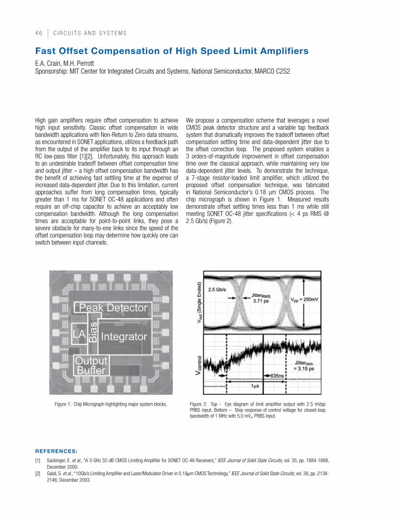
| C i r C u i t s a n d s y s t e m s
Fast Offset compensation of High speed Limit AmplifiersE.A. Crain, M.H. Perrott Sponsorship: MIT Center for Integrated Circuits and Systems, National Semiconductor, MARCO C2S2
High gain amplifiers require offset compensation to achieve high input sensitivity. Classic offset compensation in wide bandwidth applications with Non-Return to Zero data streams, as encountered in SONET applications, utilizes a feedback path from the output of the amplifier back to its input through an RC low-pass filter [1][2]. Unfortunately, this approach leads to an undesirable tradeoff between offset compensation time and output jitter – a high offset compensation bandwidth has the benefit of achieving fast settling time at the expense of increased data-dependent jitter. Due to this limitation, current approaches suffer from long compensation times, typically greater than 1 ms for SONET OC-48 applications and often require an off-chip capacitor to achieve an acceptably low compensation bandwidth. Although the long compensation times are acceptable for point-to-point links, they pose a severe obstacle for many-to-one links since the speed of the offset compensation loop may determine how quickly one can switch between input channels.
We propose a compensation scheme that leverages a novel CMOS peak detector structure and a variable tap feedback system that dramatically improves the tradeoff between offset compensation settling time and data-dependent jitter due to the offset correction loop. The proposed system enables a 3 orders-of-magnitude improvement in offset compensation time over the classical approach, while maintaining very low data-dependent jitter levels. To demonstrate the technique, a 7-stage resistor-loaded limit amplifier, which utilized the proposed offset compensation technique, was fabricated in National Semiconductor’s 0.18 µm CMOS process. The chip micrograph is shown in Figure 1. Measured results demonstrate offset settling times less than 1 ms while still meeting SONET OC-48 jitter specifications (< 4 ps RMS @ 2.5 Gb/s) (Figure 2).
Figure 1: Chip Micrograph highlighting major system blocks. Figure 2: Top - Eye diagram of limit amplifier output with 2.5 mVpp PRBS input; Bottom – Step response of control voltage for closed-loop bandwidth of 1 MHz with 5.0 mVpp PRBS input.
REFEREncEs:
[1] Sackinger, E. et al., “A 3-GHz 32-dB CMOS Limiting Amplifier for SONET OC-48 Receivers,” IEEE Journal of Solid State Circuits, vol. 35, pp. 1884-1888, December 2000.
[2] Galal, S. et al., “10Gb/s Limiting Amplifier and Laser/Modulator Driver in 0.18µm CMOS Technology,” IEEE Journal of Solid State Circuits, vol. 38, pp. 2138-2146, December 2003.
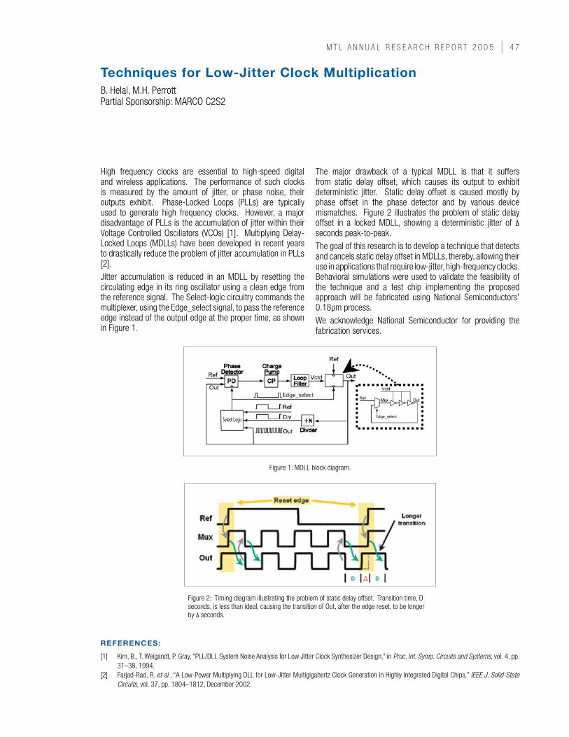
m t L a n n u a L r e s e a r C H r e P O r t 0 0 5 |
Techniques for Low-Jitter clock MultiplicationB. Helal, M.H. Perrott Partial Sponsorship: MARCO C2S2
High frequency clocks are essential to high-speed digital and wireless applications. The performance of such clocks is measured by the amount of jitter, or phase noise, their outputs exhibit. Phase-Locked Loops (PLLs) are typically used to generate high frequency clocks. However, a major disadvantage of PLLs is the accumulation of jitter within their Voltage Controlled Oscillators (VCOs) [1]. Multiplying Delay-Locked Loops (MDLLs) have been developed in recent years to drastically reduce the problem of jitter accumulation in PLLs [2]. Jitter accumulation is reduced in an MDLL by resetting the circulating edge in its ring oscillator using a clean edge from the reference signal. The Select-logic circuitry commands the multiplexer, using the Edge_select signal, to pass the reference edge instead of the output edge at the proper time, as shown in Figure 1.
The major drawback of a typical MDLL is that it suffers from static delay offset, which causes its output to exhibit deterministic jitter. Static delay offset is caused mostly by phase offset in the phase detector and by various device mismatches. Figure 2 illustrates the problem of static delay offset in a locked MDLL, showing a deterministic jitter of ∆ seconds peak-to-peak.The goal of this research is to develop a technique that detects and cancels static delay offset in MDLLs, thereby, allowing their use in applications that require low-jitter, high-frequency clocks. Behavioral simulations were used to validate the feasibility of the technique and a test chip implementing the proposed approach will be fabricated using National Semiconductors’ 0.18µm process.We acknowledge National Semiconductor for providing the fabrication services.
Figure 1: MDLL block diagram.
Figure 2: Timing diagram illustrating the problem of static delay offset. Transition time, D seconds, is less than ideal, causing the transition of Out, after the edge reset, to be longer by ∆ seconds.
REFEREncEs:
[1] Kim, B., T. Weigandt, P. Gray, “PLL/DLL System Noise Analysis for Low Jitter Clock Synthesizer Design,” in Proc. Int. Symp. Circuits and Systems, vol. 4, pp. 31–38, 1994.
[2] Farjad-Rad, R. et al., “A Low-Power Multiplying DLL for Low-Jitter Multigigahertz Clock Generation in Highly Integrated Digital Chips,” IEEE J. Solid-State Circuits, vol. 37, pp. 1804–1812, December 2002.
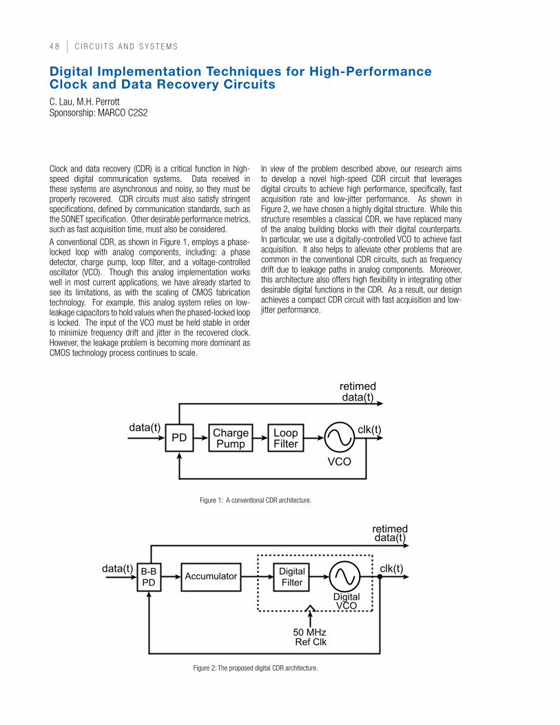
| C i r C u i t s a n d s y s t e m s
Digital Implementation Techniques for High-Performance clock and Data Recovery circuitsC. Lau, M.H. Perrott Sponsorship: MARCO C2S2
Clock and data recovery (CDR) is a critical function in high-speed digital communication systems. Data received in these systems are asynchronous and noisy, so they must be properly recovered. CDR circuits must also satisfy stringent specifications, defined by communication standards, such as the SONET specification. Other desirable performance metrics, such as fast acquisition time, must also be considered.A conventional CDR, as shown in Figure 1, employs a phase-locked loop with analog components, including: a phase detector, charge pump, loop filter, and a voltage-controlled oscillator (VCO). Though this analog implementation works well in most current applications, we have already started to see its limitations, as with the scaling of CMOS fabrication technology. For example, this analog system relies on low-leakage capacitors to hold values when the phased-locked loop is locked. The input of the VCO must be held stable in order to minimize frequency drift and jitter in the recovered clock. However, the leakage problem is becoming more dominant as CMOS technology process continues to scale.
In view of the problem described above, our research aims to develop a novel high-speed CDR circuit that leverages digital circuits to achieve high performance, specifically, fast acquisition rate and low-jitter performance. As shown in Figure 2, we have chosen a highly digital structure. While this structure resembles a classical CDR, we have replaced many of the analog building blocks with their digital counterparts. In particular, we use a digitally-controlled VCO to achieve fast acquisition. It also helps to alleviate other problems that are common in the conventional CDR circuits, such as frequency drift due to leakage paths in analog components. Moreover, this architecture also offers high flexibility in integrating other desirable digital functions in the CDR. As a result, our design achieves a compact CDR circuit with fast acquisition and low-jitter performance.
PD ChargePump
LoopFilter
data(t)
retimeddata(t)
clk(t)
VCO
Figure 1: A conventional CDR architecture.
clk(t)
retimeddata(t)
data(t) B-B
PD
DigitalVCO
Digital
FilterAccumulator
50 MHz Ref Clk
Figure 2: The proposed digital CDR architecture.
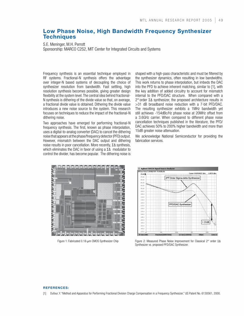
m t L a n n u a L r e s e a r C H r e P O r t 0 0 5 |
Low Phase noise, High Bandwidth Frequency synthesizer TechniquesS.E. Meninger, M.H. Perrott Sponsorship: MARCO C2S2, MIT Center for Integrated Circuits and Systems
Frequency synthesis is an essential technique employed in RF systems. Fractional-N synthesis offers the advantage over integer-N based systems of decoupling the choice of synthesizer resolution from bandwidth. Fast settling, high resolution synthesis becomes possible, giving greater design flexibility at the system level. The central idea behind fractional-N synthesis is dithering of the divide value so that, on average, a fractional divide value is obtained. Dithering the divide value introduces a new noise source to the system. This research focuses on techniques to reduce the impact of the fractional-N dithering noise.Two approaches have emerged for performing fractional-N frequency synthesis. The first, known as phase interpolation, uses a digital-to-analog converter (DAC) to cancel the dithering noise that appears at the phase/frequency detector (PFD) output. However, mismatch between the DAC output and dithering noise results in poor cancellation. More recently, Σ∆ synthesis, which eliminates the DAC in favor of using a Σ∆ modulator to control the divider, has become popular. The dithering noise is
shaped with a high-pass characteristic and must be filtered by the synthesizer dynamics, often resulting in low bandwidths. This work returns to phase interpolation, but imbeds the DAC into the PFD to achieve inherent matching, similar to [1], with the key addition of added circuitry to account for mismatch internal to the PFD/DAC structure. When compared with a 2nd order Σ∆ synthesizer, the proposed architecture results in >31 dB broadband noise reduction with a 7-bit PFD/DAC. The resulting synthesizer exhibits a 1MHz bandwidth yet still achieves -154dBc/Hz phase noise at 20MHz offset from a 3.6GHz carrier. When compared to different phase noise cancellation techniques published in the literature, the PFD/DAC achieves 50% to 200% higher bandwidth and more than 15dB greater noise attenuation. We acknowledge National Semiconductor for providing the fabrication services.
Figure 1: Fabricated 0.18-µm CMOS Synthesizer Chip Figure 2: Measured Phase Noise Improvement for Classical 2nd order Σ∆ Synthesizer vs. proposed PFD/DAC Synthesizer.
REFEREncEs:
[1] Dufour, Y. “Method and Apparatus for Performing Fractional Division Charge Compensation in a Frequency Synthesizer,” US Patent No. 6130561, 2000.
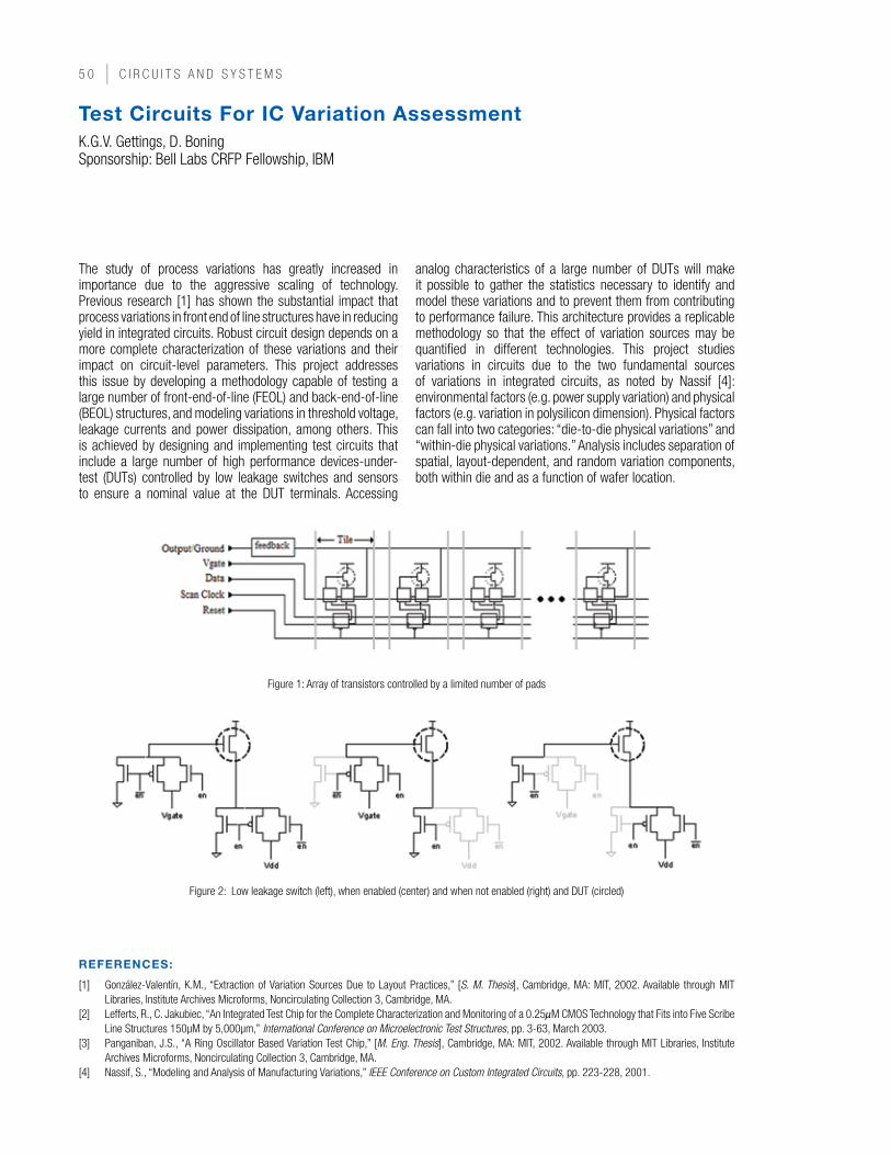
5 0 | C i r C u i t s a n d s y s t e m s
Test circuits For Ic Variation AssessmentK.G.V. Gettings, D. Boning Sponsorship: Bell Labs CRFP Fellowship, IBM
The study of process variations has greatly increased in importance due to the aggressive scaling of technology. Previous research [1] has shown the substantial impact that process variations in front end of line structures have in reducing yield in integrated circuits. Robust circuit design depends on a more complete characterization of these variations and their impact on circuit-level parameters. This project addresses this issue by developing a methodology capable of testing a large number of front-end-of-line (FEOL) and back-end-of-line (BEOL) structures, and modeling variations in threshold voltage, leakage currents and power dissipation, among others. This is achieved by designing and implementing test circuits that include a large number of high performance devices-under-test (DUTs) controlled by low leakage switches and sensors to ensure a nominal value at the DUT terminals. Accessing
analog characteristics of a large number of DUTs will make it possible to gather the statistics necessary to identify and model these variations and to prevent them from contributing to performance failure. This architecture provides a replicable methodology so that the effect of variation sources may be quantified in different technologies. This project studies variations in circuits due to the two fundamental sources of variations in integrated circuits, as noted by Nassif [4]: environmental factors (e.g. power supply variation) and physical factors (e.g. variation in polysilicon dimension). Physical factors can fall into two categories: “die-to-die physical variations” and “within-die physical variations.” Analysis includes separation of spatial, layout-dependent, and random variation components, both within die and as a function of wafer location.
Figure 1: Array of transistors controlled by a limited number of pads
Figure 2: Low leakage switch (left), when enabled (center) and when not enabled (right) and DUT (circled)
REFEREncEs:
[1] González-Valentín, K.M., “Extraction of Variation Sources Due to Layout Practices,” [S. M. Thesis], Cambridge, MA: MIT, 2002. Available through MIT Libraries, Institute Archives Microforms, Noncirculating Collection 3, Cambridge, MA.
[2] Lefferts, R., C. Jakubiec, “An Integrated Test Chip for the Complete Characterization and Monitoring of a 0.25µM CMOS Technology that Fits into Five Scribe Line Structures 150µM by 5,000µm,” International Conference on Microelectronic Test Structures, pp. 3-63, March 2003.
[3] Panganiban, J.S., “A Ring Oscillator Based Variation Test Chip,” [M. Eng. Thesis], Cambridge, MA: MIT, 2002. Available through MIT Libraries, Institute Archives Microforms, Noncirculating Collection 3, Cambridge, MA.
[4] Nassif, S., “Modeling and Analysis of Manufacturing Variations,” IEEE Conference on Custom Integrated Circuits, pp. 223-228, 2001.
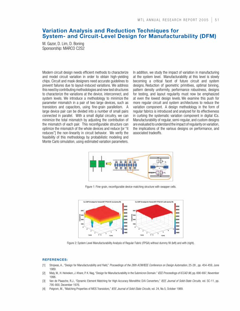
m t L a n n u a L r e s e a r C H r e P O r t 0 0 5 | 5 1
Variation Analysis and Reduction Techniques for system- and circuit-Level Design for Manufacturability (DFM)M. Gazor, D. Lim, D. Boning Sponsorship: MARCO C2S2
Modern circuit design needs efficient methods to characterize and model circuit variation in order to obtain high-yielding chips. Circuit and mask designers need accurate guidelines to prevent failures due to layout-induced variations. We address this need by contributing methodologies and new test structures to characterize the variations at the device, interconnect, and system levels. We introduce a methodology to minimize the parameter mismatch in a pair of two large devices, such as transistors and capacitors, using fine-grain parallelism. A large device pair can be divided into a number of small pairs connected in parallel. With a small digital circuitry, we can minimize the total mismatch by adjusting the contribution of the mismatch of each pair. This reconfigurable structure can optimize the mismatch of the whole devices and reduce [or “it reduces”] the non-linearity in circuit behavior. We verify the feasibility of this methodology by probabilistic modeling and Monte Carlo simulation, using estimated variation parameters.
In addition, we study the impact of variation in manufacturing at the system level. Manufacturability at this level is slowly becoming a critical facet of future circuit and system designs. Reduction of geometric primitives, optimal binning, pattern density uniformity, performance robustness, designs for testing, and layout regularity must now be emphasized at even the lowest design levels. We examine this push for more regular circuit and system architectures to reduce the variation component. A design methodology in the form of regular fabrics is introduced and analyzed for its effectiveness in curbing the systematic variation component in digital ICs. Manufacturability of regular, semi-regular, and custom designs are evaluated to understand the impact of regularity on variation, the implications of the various designs on performance, and associated tradeoffs.
Figure 1: Fine-grain, reconfigurable device-matching structure with swapper cells.
Figure 2: System Level Manufacturability Analysis of Regular Fabric (FPGA) without dummy fill (left) and with (right).
REFEREncEs:
[1] Strojwas, A., “Design for Manufacturability and Yield,” Proceedings of the 26th ACM/IEEE Conference on Design Automation, 25-28 , pp. 454-459, June 1989.
[2] Maly, W., H. Heineken, J. Khare, P. K. Nag, “Design for Manufacturability in the Submicron Domain.” IEEE Proceedings of ICCAD 96, pp. 690-697, November 1996.
[3] Van de Plaasche, R.J., “Dynamic Element Matching for High Accuracy Monolithic D/A Converters,” IEEE Journal of Solid-State Circuits, vol. SC-11, pp. 795-800, December 1976.
[4] Pelgrom, M., “Matching Properties of MOS Transistors,” IEEE Journal of Solid-State Circuits, vol. 24, No.5, October 1989.
5 | C i r C u i t s a n d s y s t e m s
Vibration-to-Electric Energy Harvesting Using a Mechanically-Varied capacitorB.C. Yen, J.H. Lang Sponsorship: Laboratory for Electromagnetic and Electronic Systems
To become a feasible alternative to electrochemical cells, energy harvesting circuits require an energy flyback mechanism that can send harvested energy into a storage node for future use. We present simulated and experimental data for a charge-constrained circuit topology containing an inductive energy flyback that periodically transfers energy harvested from a vibrational source back into a reservoir capacitor. Using a mechanical spring steel variable capacitor with capacitance variation from 415.16 pF to 884.84 pF and an out-of-plane resonant mode of 1560 Hz, the system delivers 1.8 µW at 6 V steady-state voltage to a resistive load. Because the circuit contains only one active device used for controlling the energy flyback rate, timing signal generation is greatly simplified. Unlike previous works, a source-referenced timing
scheme was explored in order to prevent unwanted energy injection into the harvesting circuit, which would artificially inflate experimental results. Finally, the system exhibits a startup voltage requirement below 89 mV, indicating that it can potentially be turned on using just a piezoelectric film.In a typical harvesting cycle, charges are delivered onto a parallel plate capacitor while the capacitance is at its maximum value. As the plates are mechanically pulled apart, vibrational energy performs positive work on the charges, which are momentarily constrained from leaving the plate. When the capacitance reaches its minimum value, the charges are moved off the parallel plate capacitor and harvested through an optimized power electronics network.
0
0.5
1
1.5
2
2.5
-10 0 10 20 30 40 50Time (sec)
0.5
Vre
s (
V)
120 mV
160 mV
200 mV
240 mV
280 mV
320 mV
Figure 1: Schematic representation of the electric energy harvesting circuit with inductive flyback. The flyback MOSFET is controlled by a clock referenced to its source to prevent undesired energy injection. Variables RW and RC model the wire loss and core loss of the flyback inductor while RP represents the resistive load being powered by the circuit.
Figure 2: Evolution of vRES for different levels of mechanical shaking. The number immediately below the curves indicates the peak-to-peak shaker amplifier input used to generate that curve. As the vibration level increases, the reservoir capacitor is able to charge up to a higher steady-state voltage, limited by nonlinear inductor core loss.
REFEREncEs:
[1] Meninger, S., J.O. Mur-Miranda, R. Amirtharajah, A. Chandrakasan, J. Lang, “Vibration-to-Electric Energy Conversion,” in International Symposium on Low Power Electronics and Design, pp. 48–53, August 1999.


![arXiv:1603.08360v4 [math.DS] 17 Mar 2018In 1880 Andrei A. Markov, a 24-year old student from St Petersburg, discovered in his master’s thesis [30] a remarkable connection between](https://static.fdocument.org/doc/165x107/5ec59f438be32d4a160cf07f/arxiv160308360v4-mathds-17-mar-2018-in-1880-andrei-a-markov-a-24-year-old.jpg)