A 750μW 3.5–4.5GHz FM-UWB transmitter · 750 W 3.5–4.5GHz FM-UWB transmitter ... review under...
8
Available online at www.sciencedirect.com ScienceDirect Journal of Electrical Systems and Information Technology 2 (2015) 133–140 A 750 W 3.5–4.5 GHz FM-UWB transmitter Mohamed Ali a,∗ , Heba Shawkey a , Abdelhalim Zekry b a Microelectronics Department, Electronics Research Institute, Egypt b Communications and Electronics Department, Ain Shams University, Egypt Available online 4 April 2015 Abstract This paper presents an ultra-low power frequency modulated ultra-wideband (FM-UWB) transmitter implemented in standard 130 nm CMOS technology. The transmitter operates in the range of 3.5–4.5 GHz with 4 GHz RF carrier frequency. The transmitter can accept input data rates up to 250 kbps. A relaxation oscillator is used to generate the subcarrier signal and a VCO for RF carrier generation. The center frequency of the VCO is periodically calibrated to avoid out of band operation. An integer-N phase-locked loop (PLL) is used for both subcarrier generation and RF VCO calibration, which needs only 500 ns to complete the calibration. A class-AB power amplifier is used to output the power under the FCC mask. The proposed FM-UWB transmitter consumes 750 W from a 1.2 V supply. © 2015 The Authors. Production and hosting by Elsevier B.V. This is an open access article under the CC BY-NC-ND license (http://creativecommons.org/licenses/by-nc-nd/4.0/). Keywords: Ultra-wideband (UWB); Frequency modulated UWB (FM-UWB); Voltage controlled oscillator (VCO); Relaxation oscillator 1. Introduction Wireless body area network (WBAN) is an emerging technology that plays very important role in a society, mainly in health services. WBAN helps in monitoring vital signs of a patient. Doctors can check the complete details of patients from remote locations and can recommend a suitable medicine. The main purpose of this technology is to reduce the load at hospitals and provide efficient healthcare facility remotely. WBAN comprises body-worn or implanted devices that continually sense vital body parameters. However, battery replacement for these devices may not be feasible or desirable which place severe constraints on the power dissipation of the radio transceiver that consumes most of total power. Moreover, WBAN is operating very close to the body. Therefore, it is a natural requirement to keep the electromagnetic pollution extremely low. These requirements make use of the ultra-wideband (UWB) technology particularly appropriate. For short range and low cost UWB systems, two UWB techniques are considered; impulse radio UWB (IR-UWB) and frequency modulated UWB (FM-UWB). The IR-UWB system transmits a sequence of extremely short pulses through ∗ Corresponding author. E-mail address: [email protected] (M. Ali). Peer review under the responsibility of Electronics Research Institute (ERI). http://dx.doi.org/10.1016/j.jesit.2015.03.012 2314-7172/© 2015 The Authors. Production and hosting by Elsevier B.V. This is an open access article under the CC BY-NC-ND license (http://creativecommons.org/licenses/by-nc-nd/4.0/).
Transcript of A 750μW 3.5–4.5GHz FM-UWB transmitter · 750 W 3.5–4.5GHz FM-UWB transmitter ... review under...
A
1cglcf©(
K
1
ifltottp
f
2(
Available online at www.sciencedirect.com
ScienceDirect
Journal of Electrical Systems and Information Technology 2 (2015) 133–140
A 750 �W 3.5–4.5 GHz FM-UWB transmitter
Mohamed Ali a,∗, Heba Shawkey a, Abdelhalim Zekry b
a Microelectronics Department, Electronics Research Institute, Egyptb Communications and Electronics Department, Ain Shams University, Egypt
Available online 4 April 2015
bstract
This paper presents an ultra-low power frequency modulated ultra-wideband (FM-UWB) transmitter implemented in standard30 nm CMOS technology. The transmitter operates in the range of 3.5–4.5 GHz with 4 GHz RF carrier frequency. The transmitteran accept input data rates up to 250 kbps. A relaxation oscillator is used to generate the subcarrier signal and a VCO for RF carriereneration. The center frequency of the VCO is periodically calibrated to avoid out of band operation. An integer-N phase-lockedoop (PLL) is used for both subcarrier generation and RF VCO calibration, which needs only 500 ns to complete the calibration. Alass-AB power amplifier is used to output the power under the FCC mask. The proposed FM-UWB transmitter consumes 750 �Wrom a 1.2 V supply.
2015 The Authors. Production and hosting by Elsevier B.V. This is an open access article under the CC BY-NC-ND licensehttp://creativecommons.org/licenses/by-nc-nd/4.0/).
eywords: Ultra-wideband (UWB); Frequency modulated UWB (FM-UWB); Voltage controlled oscillator (VCO); Relaxation oscillator
. Introduction
Wireless body area network (WBAN) is an emerging technology that plays very important role in a society, mainlyn health services. WBAN helps in monitoring vital signs of a patient. Doctors can check the complete details of patientsrom remote locations and can recommend a suitable medicine. The main purpose of this technology is to reduce theoad at hospitals and provide efficient healthcare facility remotely. WBAN comprises body-worn or implanted deviceshat continually sense vital body parameters. However, battery replacement for these devices may not be feasibler desirable which place severe constraints on the power dissipation of the radio transceiver that consumes most ofotal power. Moreover, WBAN is operating very close to the body. Therefore, it is a natural requirement to keephe electromagnetic pollution extremely low. These requirements make use of the ultra-wideband (UWB) technology
articularly appropriate.For short range and low cost UWB systems, two UWB techniques are considered; impulse radio UWB (IR-UWB) andrequency modulated UWB (FM-UWB). The IR-UWB system transmits a sequence of extremely short pulses through
∗ Corresponding author.E-mail address: [email protected] (M. Ali).Peer review under the responsibility of Electronics Research Institute (ERI).
http://dx.doi.org/10.1016/j.jesit.2015.03.012314-7172/© 2015 The Authors. Production and hosting by Elsevier B.V. This is an open access article under the CC BY-NC-ND licensehttp://creativecommons.org/licenses/by-nc-nd/4.0/).
134 M. Ali et al. / Journal of Electrical Systems and Information Technology 2 (2015) 133–140
SubcarrierOscillator
PowerAmplifier
RFOsillator
din Vm
Fig. 1. FM-UWB transmitter block diagram.
Table 1Operation of the proposed transmitter.
Control S1 S2 S3 S4 Mode
Low On On Off Off Modulation
High Off Off On On Calibrationan antenna (Win and Scholtz, 1998). Thus, IR-UWB is a carrier-less transmission technique. However, because of usinglow duty pulses, synchronization between the transmitter and the receiver becomes very challenging, which increaseshardware complexity and power consumption.
The FM-UWB system generates a constant-envelope UWB signal with wideband FM modulation, featuring a verysteep spectral roll off (Gerrits et al., 2005). Thus, the FM-UWB receiver can perform FM demodulation without alocal oscillator; carrier synchronization is not needed as the IR-UWB technique. This makes the overall system designsimple and robust.
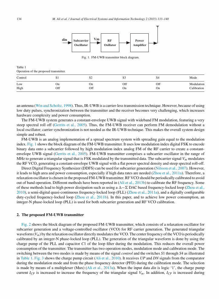
FM-UWB is an analog implementation of a spread spectrum system with spreading gain equal to the modulationindex. Fig. 1 shows the block diagram of the FM-UWB transmitter. It uses low modulation index digital FSK to encodebinary data onto a subcarrier followed by high modulation index analog FM of the RF carrier to create a constant-envelope UWB signal (Gerrits et al., 2005). FM-UWB transmitter comprises a subcarrier oscillator in the range ofMHz to generate a triangular signal that is FSK modulated by the transmitted data. The subcarrier signal Vm modulatesthe RF VCO, generating a constant-envelope UWB signal with a flat power spectral density and steep spectral roll-off.
Direct Digital Frequency Synthesizer (DDFS) can be used for subcarrier generation (Nilsson et al., 2007). However,it leads to high area and power consumption, especially if high data rates are needed (Zhou et al., 2011a). Therefore, arelaxation oscillator is chosen in the proposed FM-UWB transmitter. RF VCO should be periodically calibrated to avoidout of band operation. Different methods have been reported in (Ali et al., 2013b) to calibrate the RF frequency. Someof these methods lead to high power dissipation such as using a �−� DAC based frequency-locked loop (Zhou et al.,2010), a semi-digital quasi-continuous frequency-locked loop (FLL) (Zhou et al., 2011a), and a digitally configurableduty-cycled frequency-locked loop (Zhou et al., 2011b). In this paper, and to achieve low power consumption, aninteger-N phase-locked loop (PLL) is used for both subcarrier generation and RF VCO calibration.
2. The proposed FM-UWB transmitter
Fig. 2 shows the block diagram of the proposed FM-UWB transmitter, which consists of a relaxation oscillator forsubcarrier generation and a voltage-controlled oscillator (VCO) for RF carrier generation. The generated triangularwaveform (Vm) by the relaxation oscillator directly modulates the VCO. The center frequency of the VCO is periodicallycalibrated by an integer-N phase-locked loop (PLL). The generation of the triangular waveform is done by using thecharge pump of the PLL and capacitor C1 of the loop filter during the modulation. This reduces the overall powerconsumption of the transmitter. The transmitter has two operation modes, modulation mode and calibration mode. Theswitching between the two modes is made by means of the signal control and the switches S1 through S4 as illustratedin Table 1. Fig. 3 shows the charge pump circuit (Ali et al., 2010). It receives UP and DN signals from the comparatorduring the modulation mode and from the phase frequency detector (PFD) during the calibration mode. The selection
is made by means of a multiplexer (Mux) (Ali et al., 2013a). When the input data din is logic ‘1’, the charge pumpcurrent ICP is increased to increase the frequency of the triangular signal Vm. In addition, ICP is increased during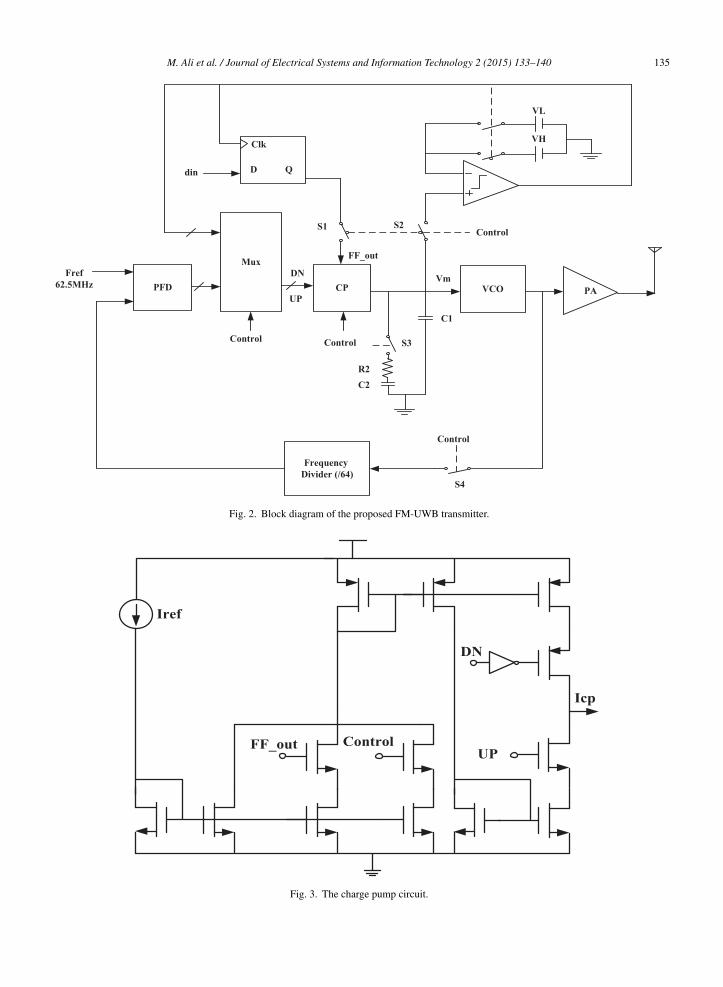
M. Ali et al. / Journal of Electrical Systems and Information Technology 2 (2015) 133–140 135
Fref62.5MHz PFD
Mux
CP VCO PA
FrequencyDivider (/64)
Control
Control
S4
S3
R2C2
C1
VL
VHClk
QD
Control
din
VmDN
UP
S1 S2
Control
FF_out
Fig. 2. Block diagram of the proposed FM-UWB transmitter.
Control
Iref
Icp
DN
UPFF_out
Fig. 3. The charge pump circuit.
136 M. Ali et al. / Journal of Electrical Systems and Information Technology 2 (2015) 133–140
Fout
Vm
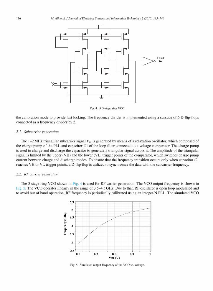
Fig. 4. A 3-stage ring VCO.
the calibration mode to provide fast locking. The frequency divider is implemented using a cascade of 6 D-flip-flopsconnected as a frequency divider by 2.
2.1. Subcarrier generation
The 1–2 MHz triangular subcarrier signal Vm is generated by means of a relaxation oscillator, which composed ofthe charge pump of the PLL and capacitor C1 of the loop filter connected to a voltage comparator. The charge pumpis used to charge and discharge the capacitor to generate a triangular signal across it. The amplitude of the triangularsignal is limited by the upper (VH) and the lower (VL) trigger points of the comparator, which switches charge pumpcurrent between charge and discharge modes. To ensure that the frequency transition occurs only when capacitor C1reaches VH or VL trigger points, a D-flip-flop is utilized to synchronize the data with the subcarrier frequency.
2.2. RF carrier generation
The 3-stage ring VCO shown in Fig. 4 is used for RF carrier generation. The VCO output frequency is shown inFig. 5. The VCO operates linearly in the range of 3.5–4.5 GHz. Due to that, RF oscillator is open loop modulated andto avoid out of band operation, RF frequency is periodically calibrated using an integer-N PLL. The simulated VCO
Fig. 5. Simulated output frequency of the VCO vs. voltage.
M. Ali et al. / Journal of Electrical Systems and Information Technology 2 (2015) 133–140 137
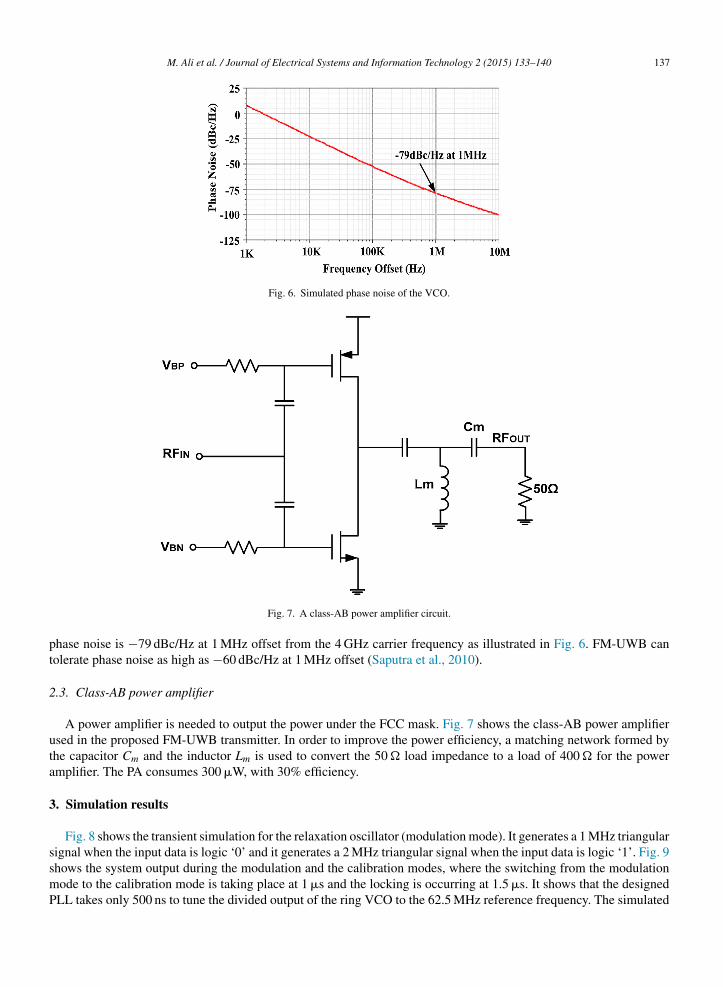
Fig. 6. Simulated phase noise of the VCO.
pt
2
uta
3
ssmP
Fig. 7. A class-AB power amplifier circuit.
hase noise is −79 dBc/Hz at 1 MHz offset from the 4 GHz carrier frequency as illustrated in Fig. 6. FM-UWB canolerate phase noise as high as −60 dBc/Hz at 1 MHz offset (Saputra et al., 2010).
.3. Class-AB power amplifier
A power amplifier is needed to output the power under the FCC mask. Fig. 7 shows the class-AB power amplifiersed in the proposed FM-UWB transmitter. In order to improve the power efficiency, a matching network formed byhe capacitor Cm and the inductor Lm is used to convert the 50 � load impedance to a load of 400 � for the powermplifier. The PA consumes 300 �W, with 30% efficiency.
. Simulation results
Fig. 8 shows the transient simulation for the relaxation oscillator (modulation mode). It generates a 1 MHz triangular
ignal when the input data is logic ‘0’ and it generates a 2 MHz triangular signal when the input data is logic ‘1’. Fig. 9hows the system output during the modulation and the calibration modes, where the switching from the modulationode to the calibration mode is taking place at 1 �s and the locking is occurring at 1.5 �s. It shows that the designedLL takes only 500 ns to tune the divided output of the ring VCO to the 62.5 MHz reference frequency. The simulated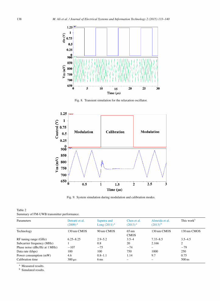
138 M. Ali et al. / Journal of Electrical Systems and Information Technology 2 (2015) 133–140
Fig. 8. Transient simulation for the relaxation oscillator.
Fig. 9. System simulation during modulation and calibration modes.
Table 2Summary of FM-UWB transmitter performance.
Parameters Detratti et al.(2009) a
Saputra andLong (2011) a
Chen et al.(2013) a
Almeida et al.(2013) b
This workb
Technology 130 nm CMOS 90 nm CMOS 65 nmCMOS
130 nm CMOS 130 nm CMOS
RF tuning range (GHz) 6.25–8.25 2.9–5.2 3.5–4 7.33–8.5 3.5–4.5Subcarrier frequency (MHz) 1 0.8 20 2.166 2Phase noise (dBc/Hz at 1 MHz) −107 −75 −74 – −79Data rate (kbps) 100 100 750 1000 250Power consumption (mW) 4.6 0.8–1.1 1.14 9.7 0.75Calibration time 300 �s 6 ms – – 500 ns
a Measured results.b Simulated results.
M. Ali et al. / Journal of Electrical Systems and Information Technology 2 (2015) 133–140 139
Fott
4
mgcfV
R
A
AAAC
D
G
N
S
SWZ
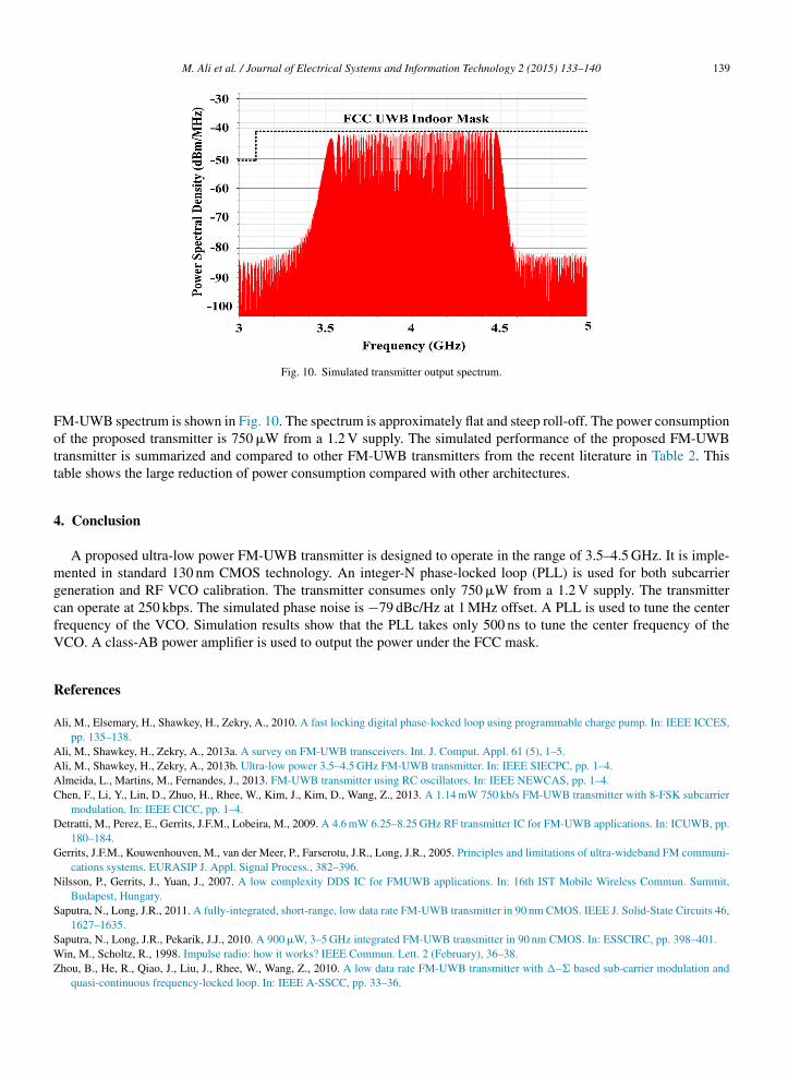
Fig. 10. Simulated transmitter output spectrum.
M-UWB spectrum is shown in Fig. 10. The spectrum is approximately flat and steep roll-off. The power consumptionf the proposed transmitter is 750 �W from a 1.2 V supply. The simulated performance of the proposed FM-UWBransmitter is summarized and compared to other FM-UWB transmitters from the recent literature in Table 2. Thisable shows the large reduction of power consumption compared with other architectures.
. Conclusion
A proposed ultra-low power FM-UWB transmitter is designed to operate in the range of 3.5–4.5 GHz. It is imple-ented in standard 130 nm CMOS technology. An integer-N phase-locked loop (PLL) is used for both subcarrier
eneration and RF VCO calibration. The transmitter consumes only 750 �W from a 1.2 V supply. The transmitteran operate at 250 kbps. The simulated phase noise is −79 dBc/Hz at 1 MHz offset. A PLL is used to tune the centerrequency of the VCO. Simulation results show that the PLL takes only 500 ns to tune the center frequency of theCO. A class-AB power amplifier is used to output the power under the FCC mask.
eferences
li, M., Elsemary, H., Shawkey, H., Zekry, A., 2010. A fast locking digital phase-locked loop using programmable charge pump. In: IEEE ICCES,pp. 135–138.
li, M., Shawkey, H., Zekry, A., 2013a. A survey on FM-UWB transceivers. Int. J. Comput. Appl. 61 (5), 1–5.li, M., Shawkey, H., Zekry, A., 2013b. Ultra-low power 3.5–4.5 GHz FM-UWB transmitter. In: IEEE SIECPC, pp. 1–4.lmeida, L., Martins, M., Fernandes, J., 2013. FM-UWB transmitter using RC oscillators. In: IEEE NEWCAS, pp. 1–4.hen, F., Li, Y., Lin, D., Zhuo, H., Rhee, W., Kim, J., Kim, D., Wang, Z., 2013. A 1.14 mW 750 kb/s FM-UWB transmitter with 8-FSK subcarrier
modulation. In: IEEE CICC, pp. 1–4.etratti, M., Perez, E., Gerrits, J.F.M., Lobeira, M., 2009. A 4.6 mW 6.25–8.25 GHz RF transmitter IC for FM-UWB applications. In: ICUWB, pp.
180–184.errits, J.F.M., Kouwenhouven, M., van der Meer, P., Farserotu, J.R., Long, J.R., 2005. Principles and limitations of ultra-wideband FM communi-
cations systems. EURASIP J. Appl. Signal Process., 382–396.ilsson, P., Gerrits, J., Yuan, J., 2007. A low complexity DDS IC for FMUWB applications. In: 16th IST Mobile Wireless Commun. Summit,
Budapest, Hungary.
aputra, N., Long, J.R., 2011. A fully-integrated, short-range, low data rate FM-UWB transmitter in 90 nm CMOS. IEEE J. Solid-State Circuits 46,1627–1635.aputra, N., Long, J.R., Pekarik, J.J., 2010. A 900 �W, 3–5 GHz integrated FM-UWB transmitter in 90 nm CMOS. In: ESSCIRC, pp. 398–401.in, M., Scholtz, R., 1998. Impulse radio: how it works? IEEE Commun. Lett. 2 (February), 36–38.
hou, B., He, R., Qiao, J., Liu, J., Rhee, W., Wang, Z., 2010. A low data rate FM-UWB transmitter with �–� based sub-carrier modulation andquasi-continuous frequency-locked loop. In: IEEE A-SSCC, pp. 33–36.
140 M. Ali et al. / Journal of Electrical Systems and Information Technology 2 (2015) 133–140
Zhou, B., Lv, H., Wang, M., Liu, J., Rhee, W., Li, Y., Kim, D., Wang, Z., 2011a. A 1 Mb/s 3.2-4.4 GHz reconfigurable FM-UWB transmitter in0.18 �m CMOS. In: IEEE RFIC, pp. 1–4.
Zhou, B., Rhee, W., Wang, Z., 2011b. Reconfigurable FM-UWB transmitter. Electron. Lett. 47 (10).
Mohamed Ali received the B.S. degree from faculty of Electronics Engineering, Menofia University, Egypt, in 2005, andthe M.S. degree in electronics and communication engineering from Ain Shams University, Egypt, in 2011. He is currentlypursuing the Ph.D. degree at Ain Shams University, Egypt. He has been working in Electronics Research Institute since2007. His current research interests include analog and RF circuit and system design.
Heba Shawkey was born in Assyout, Egypt, 1971. She received her M.Sc. in electronics and communication engineeringfrom Ain Shams University in 2000 and her Ph.D. in electronics and communication engineering from Cairo University in2005. She has been working in Electronics Research Institute since 1994. Her main interests are RF circuits and systemsdesign. She also has many publications in Networks On Chips and low power circuit design.
Abdelhalim Zekry is a professor of electronics at faculty of Engineering, Ain Shams University, Cairo, Egypt. He workedas a staff member on several universities. He published more than 150 conference and periodical papers. He also supervisedmore than 70 Master thesis and 25 Doctorate. Prof. Zekry focuses his research programs on the field of microelectronicsand electronic applications including communications and photovoltaics. He likes the solid-state electronics very much.