A 1.8 GHz LC-Voltage Controlled Oscillator Using On-Chip ...
109
University of Tennessee, Knoxville University of Tennessee, Knoxville TRACE: Tennessee Research and Creative TRACE: Tennessee Research and Creative Exchange Exchange Masters Theses Graduate School 5-2004 A 1.8 GHz LC-Voltage Controlled Oscillator Using On-Chip A 1.8 GHz LC-Voltage Controlled Oscillator Using On-Chip Inductors and Body Driven Varactors in CMOS 0.35 μm process Inductors and Body Driven Varactors in CMOS 0.35 m process Lakshmipriya Seshan University of Tennessee - Knoxville Follow this and additional works at: https://trace.tennessee.edu/utk_gradthes Part of the Electrical and Electronics Commons Recommended Citation Recommended Citation Seshan, Lakshmipriya, "A 1.8 GHz LC-Voltage Controlled Oscillator Using On-Chip Inductors and Body Driven Varactors in CMOS 0.35 μm process. " Master's Thesis, University of Tennessee, 2004. https://trace.tennessee.edu/utk_gradthes/2201 This Thesis is brought to you for free and open access by the Graduate School at TRACE: Tennessee Research and Creative Exchange. It has been accepted for inclusion in Masters Theses by an authorized administrator of TRACE: Tennessee Research and Creative Exchange. For more information, please contact [email protected].
Transcript of A 1.8 GHz LC-Voltage Controlled Oscillator Using On-Chip ...
University of Tennessee, Knoxville University of Tennessee, Knoxville
TRACE: Tennessee Research and Creative TRACE: Tennessee Research and Creative
Exchange Exchange
Masters Theses Graduate School
5-2004
A 1.8 GHz LC-Voltage Controlled Oscillator Using On-Chip A 1.8 GHz LC-Voltage Controlled Oscillator Using On-Chip
Inductors and Body Driven Varactors in CMOS 0.35 μm process Inductors and Body Driven Varactors in CMOS 0.35 m process
Lakshmipriya Seshan University of Tennessee - Knoxville
Follow this and additional works at: https://trace.tennessee.edu/utk_gradthes
Part of the Electrical and Electronics Commons
Recommended Citation Recommended Citation Seshan, Lakshmipriya, "A 1.8 GHz LC-Voltage Controlled Oscillator Using On-Chip Inductors and Body Driven Varactors in CMOS 0.35 μm process. " Master's Thesis, University of Tennessee, 2004. https://trace.tennessee.edu/utk_gradthes/2201
This Thesis is brought to you for free and open access by the Graduate School at TRACE: Tennessee Research and Creative Exchange. It has been accepted for inclusion in Masters Theses by an authorized administrator of TRACE: Tennessee Research and Creative Exchange. For more information, please contact [email protected].
To the Graduate Council:
I am submitting herewith a thesis written by Lakshmipriya Seshan entitled "A 1.8 GHz LC-
Voltage Controlled Oscillator Using On-Chip Inductors and Body Driven Varactors in CMOS 0.35
μm process." I have examined the final electronic copy of this thesis for form and content and
recommend that it be accepted in partial fulfillment of the requirements for the degree of
Master of Science, with a major in Electrical Engineering.
Syed K. Islam, Major Professor
We have read this thesis and recommend its acceptance:
Benjamin J. Blalock, Donald W. Bouldin
Accepted for the Council:
Carolyn R. Hodges
Vice Provost and Dean of the Graduate School
(Original signatures are on file with official student records.)
To the Graduate Council: I am submitting herewith a thesis written by Lakshmipriya Seshan entitled “A 1.8 GHz
LC-Voltage Controlled Oscillator Using On-Chip Inductors and Body Driven Varactors
in CMOS 0.35 µm process.” I have examined the final electronic copy of this thesis for
form and content and recommend that it be accepted in partial fulfillment of the
requirements for the degree of Master of Science, with a major in Electrical Engineering.
Syed K. Islam
Major Professor
We have read this thesis
and recommend its acceptance: Benjamin J. Blalock Donald W. Bouldin
Accepted for the Council:
Anne Mayhew
Vice Chancellor and Dean of Graduate Studies
(Original signatures are on file with official student records.)
A 1.8 GHz LC-Voltage Controlled Oscillator Using On-Chip Inductors and Body Driven Varactors in
CMOS 0.35 µm process
A Thesis
Presented for the
Master of Science Degree
The University of Tennessee, Knoxville
Lakshmipriya Seshan May 2004
ii
ACKNOWLEDGEMENTS
I would like to express my sincere gratitude and appreciation to my supervisor, Dr. Syed.
K. Islam for providing me the opportunity to pursue my Master’s at this university and
for guiding me towards the completion of this thesis. Special thanks to Dr. Benjamin J.
Blalock for teaching me the fundamentals of Analog IC Design, and also for providing
valuable suggestions for my research work. I would also like to thank Dr. Donald W.
Bouldin for teaching me the fundamentals of VLSI design and for serving on my
committee. A special thanks goes to the present and former members of my research
group for helping me in every instant of my thesis work. I also wish to thank my fellow
graduate students and all the faculty and staff in our department for making my graduate
study such a rewarding experience.
I would like to take this opportunity to thank Analog Devices Inc (ADI) for selecting me
for the UT ADI Fellowship, 2002. A thank you to Bryce Gray & Kevin Behel for
selecting me for the fellowship program. The fellowship was great help for my research
work. Special thanks to thank Carl Moreland for assisting me in every stage of my thesis
work. I would also like to thank MOSIS for helping me fabricate my design using the
MEP Educational Program.
Thanks to the destiny for blessing me with such a wonderful family, Amma, Appa and
Prabhu for providing sustaining love and inspiration in my joy and solace. Last but not
the least a big thanks to all my friends in Knoxville.
iii
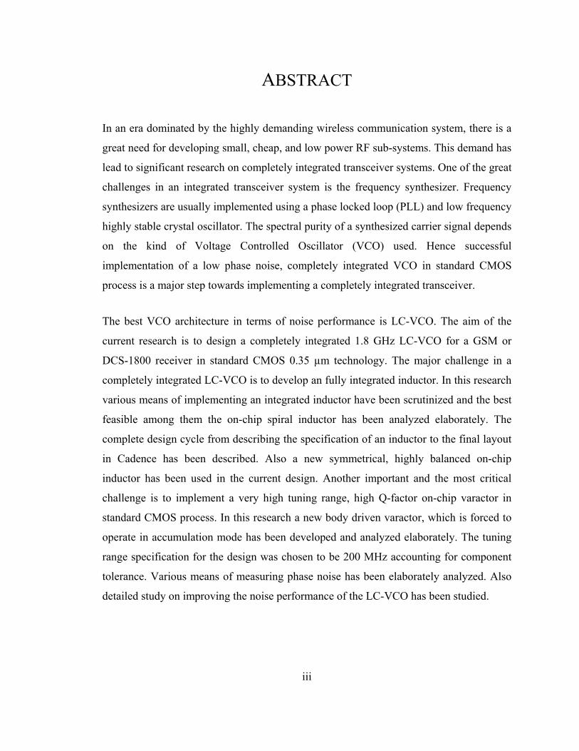
ABSTRACT
In an era dominated by the highly demanding wireless communication system, there is a
great need for developing small, cheap, and low power RF sub-systems. This demand has
lead to significant research on completely integrated transceiver systems. One of the great
challenges in an integrated transceiver system is the frequency synthesizer. Frequency
synthesizers are usually implemented using a phase locked loop (PLL) and low frequency
highly stable crystal oscillator. The spectral purity of a synthesized carrier signal depends
on the kind of Voltage Controlled Oscillator (VCO) used. Hence successful
implementation of a low phase noise, completely integrated VCO in standard CMOS
process is a major step towards implementing a completely integrated transceiver.
The best VCO architecture in terms of noise performance is LC-VCO. The aim of the
current research is to design a completely integrated 1.8 GHz LC-VCO for a GSM or
DCS-1800 receiver in standard CMOS 0.35 µm technology. The major challenge in a
completely integrated LC-VCO is to develop an fully integrated inductor. In this research
various means of implementing an integrated inductor have been scrutinized and the best
feasible among them the on-chip spiral inductor has been analyzed elaborately. The
complete design cycle from describing the specification of an inductor to the final layout
in Cadence has been described. Also a new symmetrical, highly balanced on-chip
inductor has been used in the current design. Another important and the most critical
challenge is to implement a very high tuning range, high Q-factor on-chip varactor in
standard CMOS process. In this research a new body driven varactor, which is forced to
operate in accumulation mode has been developed and analyzed elaborately. The tuning
range specification for the design was chosen to be 200 MHz accounting for component
tolerance. Various means of measuring phase noise has been elaborately analyzed. Also
detailed study on improving the noise performance of the LC-VCO has been studied.
iv
CONTENTS
1 INTRODUCTION................................................................................................. 1
1.1 Overview................................................................................................................. 1
1.2 Motivation............................................................................................................... 1
1.3 Contribution of current work .................................................................................. 3
1.4 Organization of this thesis ...................................................................................... 4
2 VOLTAGE CONTROLLED OSCILLATORS ................................................. 6
2.1 History..................................................................................................................... 6
2.2 Phase Locked Loop................................................................................................. 8
2.3 Types of VCO......................................................................................................... 9
2.4 Analysis................................................................................................................. 10
2.4.1 Quality factor of an oscillator ...................................................................... 13
2.5 Principle of LC oscillator...................................................................................... 16
2.6 Other VCO architectures....................................................................................... 19
2.6.1 Ring oscillator............................................................................................... 19
2.6.2 Relaxation oscillator ..................................................................................... 22
2.6.3 Interpolative oscillator.................................................................................. 23
3 INTEGRATED INDUCTORS AND VARACTORS....................................... 24
3.1 Importance of integrated inductor......................................................................... 24
3.2 Integrated inductor design..................................................................................... 26
3.2.1 Active inductors ............................................................................................ 27
3.2.2 Bondwire inductors ....................................................................................... 29
v
3.2.3 Inductor on a package .................................................................................. 32
3.2.4 Spiral inductors............................................................................................. 33
3.3 Loss mechanism of on-chip inductor.................................................................... 35
3.4 On-chip spiral inductor modeling ......................................................................... 37
3.5 Planar inductor structures ................................................................................ 42
3.5.1 Planar circular spiral ................................................................................... 42
3.5.2 Tapered inductor........................................................................................... 43
3.5.3 Symmetrical inductor .................................................................................... 43
3.5.4 Transformer .................................................................................................. 45
3.6 Design guide to on-chip CMOS inductors ..................................................... 46
3.6.1 Process .......................................................................................................... 46
3.6.2 Q-factor......................................................................................................... 46
3.6.3 Layer topology .............................................................................................. 46
3.6.4 Inductor area ................................................................................................ 47
3.7 ASITIC.................................................................................................................. 47
3.7.1 ASITIC organization ..................................................................................... 49
3.8 Varactor realization............................................................................................... 51
3.8.1 Varicap diodes .............................................................................................. 52
3.8.2 Conventional MOS varactor ......................................................................... 53
3.8.3 Body driven MOS varactor ........................................................................... 56
3.9 Body driven MOS varactor modeling................................................................... 59
4 1.8 GHZ LC VCO DESIGN AND RESULTS.................................................. 63
4.1 Design ................................................................................................................... 63
vi
4.1.1 Tail current source........................................................................................ 64
4.1.2 Tank design ................................................................................................... 64
4.1.3 Buffer design ................................................................................................. 67
4.2 Integrated circuit layout ........................................................................................ 68
4.3 Simulation results.................................................................................................. 72
4.4 Phase noise............................................................................................................ 74
4.4.1 Phase noise behavior of LC-VCO................................................................. 76
5 CONCLUSION AND FUTURE WORK .......................................................... 82
5.1 Conclusion ............................................................................................................ 82
5.2 Future work........................................................................................................... 82
REFERENCES................................................................................................................ 84
APPENDICES................................................................................................................. 89
APPENDIX A : Spice netlist ............................................................................................ 90
APPENDIX B: Inductor layout using ASITIC................................................................ 92
APPENDIX C: Phase noise calculation............................................................................ 94
VITA................................................................................................................................. 97
vii
LIST OF TABLES
Table 1.1: Comparison of previous VCO implementation ................................................. 4 Table 2.1: VCO comparison ............................................................................................. 10 Table 3.1: Inductance variation with frequency ............................................................... 25 Table 3.2 : Summary of capacitance................................................................................. 62 Table 4.1: Design summary .............................................................................................. 72 Table 4.2 : Jitter summary ................................................................................................ 79
viii
LIST OF FIGURES
Figure 1.1 : GSM base station receiver [1] ......................................................................... 2 Figure 2.1 : Chronological changes in VCO....................................................................... 7 Figure 2.2 : PLL block diagram.......................................................................................... 8 Figure 2.3 : Basic positive feedback network................................................................... 11 Figure 2.4 : One port network feedback model ................................................................ 12 Figure 2.5 : Modified VCO mathematical model ............................................................. 13 Figure 2.6: Differential LC-VCO topology ...................................................................... 14 Figure 2.7: Open loop tank circuit .................................................................................... 15 Figure 2.8: Functional block diagram of a LC oscillator.................................................. 17 Figure 2.9 : Simulated drain currents in current mode ..................................................... 18 Figure 2.10 : Simulated tank voltage vs tail current ......................................................... 19 Figure 2.11 : A ring oscillator realized using five digital inverters .................................. 20 Figure 2.12 : A fully differential inverter with a programmable delay ............................ 21 Figure 2.13 : A CMOS relaxation oscillator..................................................................... 22 Figure 2.14 : Interpolative oscillator................................................................................. 23 Figure 3.1 : Typical bonding diagram............................................................................... 25 Figure 3.2: A gyrator based active inductor...................................................................... 27 Figure 3.3: Equivalent noise circuit .................................................................................. 28 Figure 3.4 : Differential bondwire inductors .................................................................... 30 Figure 3.5: Bondwire inductor cross-section .................................................................... 31 Figure 3.6: MCM-D layer architecture ............................................................................. 32 Figure 3.7: Photograph of a high Q spiral inductor in MCM-D ....................................... 33 Figure 3.8: Cross-section of typical CMOS substrate layer ............................................. 34 Figure 3.9: Loss current distribution of a spiral inductor ................................................. 36 Figure 3.10 : Equivalent model of a spiral inductor ........................................................ 37 Figure 3.11 : Simplified model of a spiral inductor.......................................................... 38 Figure 3.12: Inductance variation with physical dimensions............................................ 39 Figure 3.13 : Series Resistance variation with frequency................................................. 40 Figure 3.14: q-factor variation with frequency ................................................................. 42 Figure 3.15: Circular spiral ............................................................................................... 43 Figure 3.16: Tapered spiral ............................................................................................... 44 Figure 3.17: Poly-symmetrical spiral................................................................................ 44 Figure 3.18 : Square spiral transformer ............................................................................ 45 Figure 3.19 : Different domains in ASITIC...................................................................... 48 Figure 3.20 : Block diagram of the ASITIC modules....................................................... 50 Figure 3.21 : Capacitive variation of a MOS varactor...................................................... 54 Figure 3.22 : Q-factor variation of MOS varactor ............................................................ 55 Figure 3.23 : Tuning characteristics of a MOS varactor................................................... 56 Figure 3.24 : Differential body driven varactor and its equivalent circuit........................ 57 Figure 3.25: Capacitive variation with control voltage .................................................... 58 Figure 3.26 : Q-factor variation with control voltage ....................................................... 58 Figure 3.27 : Simplified model of the body driven varactor............................................. 61
ix
Figure 4.1: Conceptual block diagram.............................................................................. 63 Figure 4.2: Current source schematic ............................................................................... 65 Figure 4.3: Tank circuit schematic.................................................................................... 67 Figure 4.4: Buffer schematic............................................................................................. 68 Figure 4.5: Layout imported from ASITIC....................................................................... 69 Figure 4.6 : Modified symmetrical inductor layout .......................................................... 69 Figure 4.7: Padframe layout.............................................................................................. 70 Figure 4.8: Complete layout ............................................................................................. 71 Figure 4.9: Large signal transient response ...................................................................... 73 Figure 4.10 : Tuning characteristics of LC-VCO ............................................................. 74 Figure 4.11: Spectral content ............................................................................................ 75 Figure 4.12 : Practical carrier signal in time domain........................................................ 76 Figure 4.13 : Phase noise spectre plot............................................................................... 80 Figure 4.14: Phase noise variation @ 1 kHz offset .......................................................... 81 Figure 4.15: Phase noise variation @ 1 MHz offset ......................................................... 81
1
1 INTRODUCTION
1.1 Overview If each decade has its name dedicated to a scientific advancement, then the nineties will
certainly be known for making everyday life wireless. This has been accomplished by the
technological revolution from the large, bulky, noisy, and costly mobile phone of eighties
to the GSM (Global System for Mobile Communication) phones that fit into the pocket
while offering high quality connection, several hours of talk time and at significantly
lower cost. The demand for high bandwidth communication channels have further
exploded with the advent of the Internet. The rapid advancement from professional
wireless users to a real mass market was achieved mainly due to the high-density
integrated circuit and efficient digital modulation schemes. Transceiver which forms the
main unit in a wireless system is migrating from a multi-chip system to a single-chip with
minimum external components. A major challenge in integrated transceiver is to
accomplish low noise, low power, and high frequency optimized sub-blocks in a single
unified technology. This has been the driving force behind the scaled CMOS technology.
All these developments will lead to the long time goal to produce an omniscient wireless
terminal that can handle voice, data and video along with amazing computational speed.
1.2 Motivation A transceiver (transmitter-receiver) is the basic building block that interfaces between the
user and the transmission medium in wireless communication. It consists of three blocks.
The user block interfaces between the raw data and its digital data representation. The
back-end module modulates or demodulates the digital data to and from the user interface
by a suitable transmission technique such as GMSK, QPSK. The front end is the building
block that does conversion between the high frequency wireless signals and the low
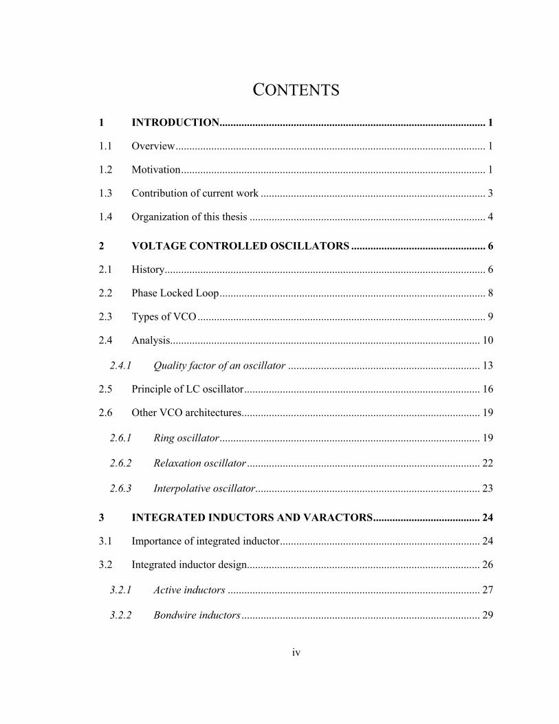
frequency baseband signal. Figure 1.1 shows a simplified GSM1800 receiver architecture
[1]. For the receiver system the front-end amplifies the wireless signal using a low noise
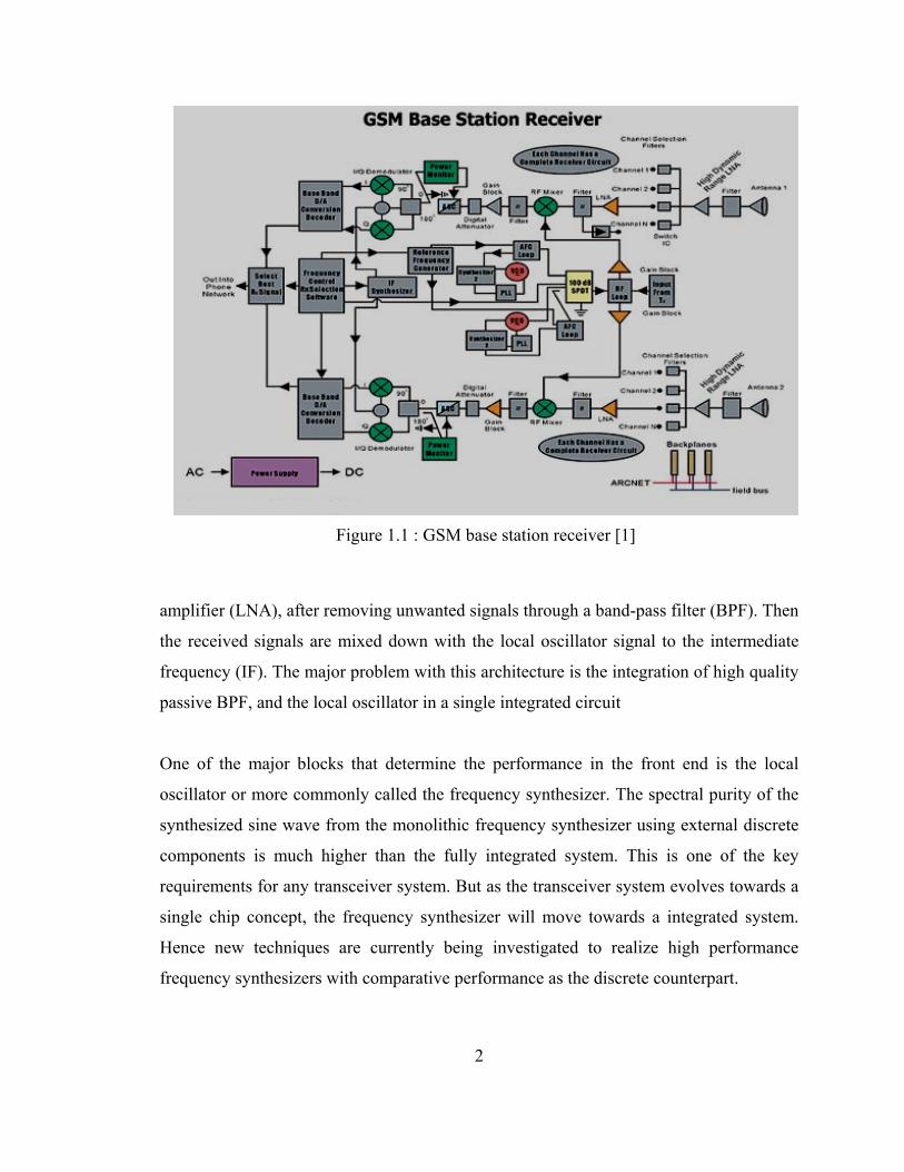
2
amplifier (LNA), after removing unwanted signals through a band-pass filter (BPF). Then
the received signals are mixed down with the local oscillator signal to the intermediate
frequency (IF). The major problem with this architecture is the integration of high quality
passive BPF, and the local oscillator in a single integrated circuit
One of the major blocks that determine the performance in the front end is the local
oscillator or more commonly called the frequency synthesizer. The spectral purity of the
synthesized sine wave from the monolithic frequency synthesizer using external discrete
components is much higher than the fully integrated system. This is one of the key
requirements for any transceiver system. But as the transceiver system evolves towards a
single chip concept, the frequency synthesizer will move towards a integrated system.
Hence new techniques are currently being investigated to realize high performance
frequency synthesizers with comparative performance as the discrete counterpart.
Figure 1.1 : GSM base station receiver [1]
3
For the lower end of the spectrum a very stable crystal oscillator can be used to generate
a very accurate reference carrier signal. For higher frequencies ( > few hundred MHz) the
quality of the crystal resonator degrades due to the physical limitations and material
properties. Many wireless applications require programmable carrier frequencies. The
cost and board space of a multitude of crystals would be strenuous. Hence indirect
frequency synthesizers based on a phase locked loop (PLL) are widely employed. In a
PLL a high frequency RF signal is locked to a precise low frequency clock by means of a
RF oscillator whose frequency is varied using a control signal embedded in a feedback
loop. The critical block in the PLL architecture is the RF oscillator or more commonly
known as the voltage controlled oscillator (VCO). The current research will focus on the
silicon implementation of VCO for wireless application.
There are different ways of implementing a tuned VCO. Traditionally they were
implemented easy to use hybrid models, but were bulky and expensive. High volume
markets are governed by the price, package, performance and power. Integration reduces
production cost due to large volume production. Integration also reduces the interface
cost and allows cheaper packaging solutions. The performance depends on the choice of
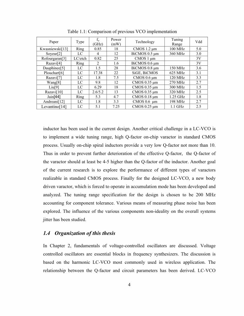
the IC technology. Table 1.1 provides a comparison of the performance of different VCO
implementation reported in the literature during the time period 1995 – 2003.
1.3 Contribution of current work Currently a lot of research is being pursued in developing RF circuits for the most widely
used communication standards namely Digital Cellular System (DCS-1800) and GSM
1800 communication standard. The aim of the current research is to design a completely
integrated 1.8 GHz LC-VCO for a GSM or DCS-1800 receiver in standard CMOS 0.35
µm technology. The major challenge in a completely integrated LC-VCO is to implement
an integrated inductor. In this research various means of implementing an inductor has
been scrutinized and best feasible among them the spiral inductor has been analyzed.
Complete design cycle from describing the specification of an inductor to the final layout
in Cadence has been described. Also a new symmetrical, highly balanced on-chip
4
inductor has been used in the current design. Another critical challenge in a LC-VCO is
to implement a wide tuning range, high Q-factor on-chip varactor in standard CMOS
process. Usually on-chip spiral inductors provide a very low Q-factor not more than 10.
Thus in order to prevent further deterioration of the effective Q-factor, the Q-factor of
the varactor should at least be 4-5 higher than the Q-factor of the inductor. Another goal
of the current research is to explore the performance of different types of varactors
realizable in standard CMOS process. Finally for the designed LC-VCO, a new body
driven varactor, which is forced to operate in accumulation mode has been developed and
analyzed. The tuning range specification for the design is chosen to be 200 MHz
accounting for component tolerance. Various means of measuring phase noise has been
explored. The influence of the various components non-ideality on the overall systems
jitter has been studied.
1.4 Organization of this thesis In Chapter 2, fundamentals of voltage-controlled oscillators are discussed. Voltage
controlled oscillators are essential blocks in frequency synthesizers. The discussion is
based on the harmonic LC-VCO most commonly used in wireless application. The
relationship between the Q-factor and circuit parameters has been derived. LC-VCO
Table 1.1: Comparison of previous VCO implementation
Paper Type fo (GHz)
Power (mW) Technology Tuning
Range Vdd
Kwasniewski[13] Ring 0.85 18 CMOS 1.2 µm 100 MHz 5.0 Soyeur[2] LC 4 12 BiCMOS 0.5 µm 360 MHz 3.0
Rofourgaran[3] LC/etch 0.82 25 CMOS 1 µm 3V Razavi[4] Ring 2 1.6 BiCMOS 0.6 µm 3V
Dauphinee[5] LC 1.5 28 BiCMOS 0.8 µm 150 MHz 3.6 Plouchart[6] LC 17.38 22 SiGE, BiCMOS 625 MHz 3.1
Razavi[7] LC 1.8 7.5 CMOS 0.6 µm 120 MHz 3.3 Wang[8] LC 9.8 12 CMOS 0.35 µm 270 MHz 2.7
Liu[9] LC 6.29 18 CMOS 0.35 µm 300 MHz 1.5 Razavi[10] LC 2.6/5.2 13 CMOS 0.35 µm 320 MHz 2.5
Jain[44] Ring 5.3 4.7 CMOS 0.18 µm 1.25 GHz 1.8 Andreani[12] LC 1.8 3.3 CMOS 0.6 µm 198 MHz 2.7
Levantino[14] LC 5.1 7.25 CMOS 0.25 µm 1.1 GHz 2.5
5
working principle along with different regions of operation has been described. Other
types of VCO architecture have also been explained and their shortcoming for wireless
application has been studied.
Chapter 3 discusses the different techniques for realizing an integrated inductor and high
Q-factor varactor. Four different types of integrated inductors have been analyzed and the
best feasible among them the spiral inductor in terms of practical large-scale
implementation has been analyzed deeply. A general overview of ASITIC, the modeling
tool used for analyzing the spiral inductors has been presented. Different types of
conventional varactors in standard CMOS process have been compared. Elaborate
analysis on the new body driven varactor operating in accumulation mode is also
presented.
Chapter 4 begins with a discussion on the design of 1.8 GHz LC-VCO. Complete design
steps from the specification of physical dimension to the final layout in Cadence have
been presented. A general overview on the phase noise performance of the LC-VCO is
also described. Finally, a better means of analyzing jitter based on the non-ideality of the
individual tank elements has been developed.
Chapter 5 summarizes the design and provides suggestions for future work.
6
2 VOLTAGE CONTROLLED OSCILLATORS
Controlled Oscillators are autonomous circuits that produce a stable periodically time
varying waveforms whose frequency of oscillation varies with the change in the control
signal. The control signal can be the voltage or the current thus leading to two different
types of controlled oscillators called the voltage-controlled oscillators (VCO) and the
current controlled oscillators. In this chapter, oscillator design equations and other
performance parameters will be derived based on the VCO. The same theory and the
performance constraints are also valid for the current controlled oscillators.
2.1 History
The current stand of VCO owes its heritage to Edwing Armstrong who discovered that
there needs to be a method to the change the frequency of an oscillator to maintain a
constant IF frequency for varying input frequencies (Superhetrodyne principle). He
designed a vacuum tube called Audion which used a spark-gap oscillator for varying the
frequency. The basic oscillator topology was later improved by Rober. V. J. Hartley, who
designed the first tuned oscillator using an amplifying device and inductive feedback, to
recreate the damped tuned oscillations. This sparkling network lead way to many widely
used topologies like Colpitts, Clapps, Armstrong, and Pierce all using some tuned
network in the feedback loop, where either a capacitor or an inductor value would be
varied mechanically for achieving variable frequency. Like many other inventions in
electronics all these earlier topologies were very bulky, expensive and consumed huge
amount of power making them viable for military applications only. The commercial
utilization of these concepts became viable after the invention of bipolar transistors
(1950) and the discovery of reverse biased pn junction for variable capacitors (1960’s).
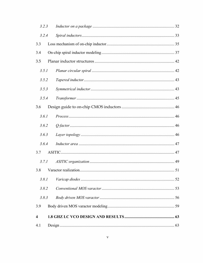
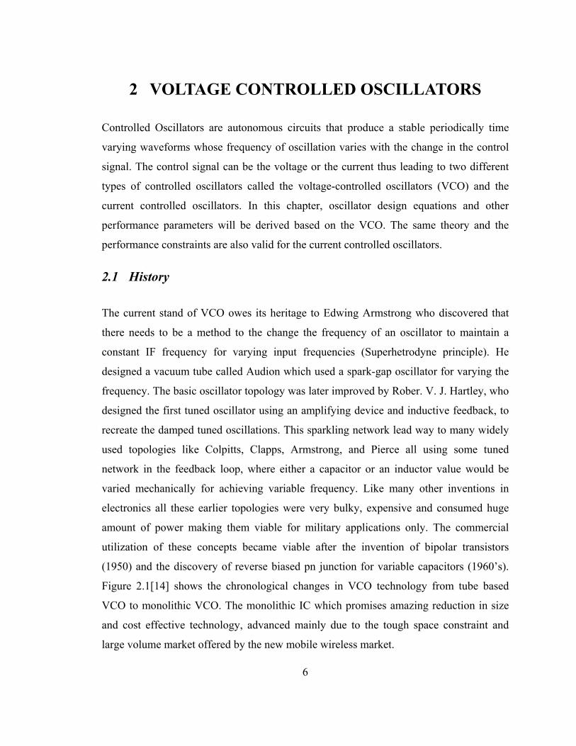
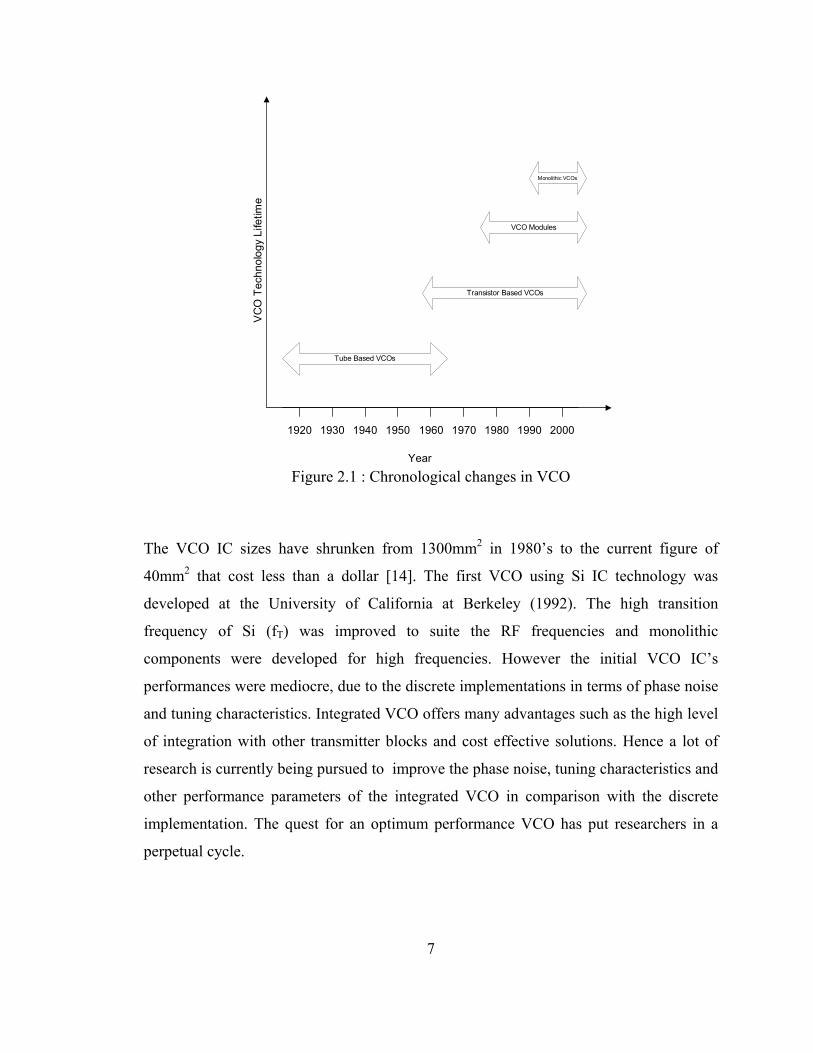
Figure 2.1[14] shows the chronological changes in VCO technology from tube based
VCO to monolithic VCO. The monolithic IC which promises amazing reduction in size
and cost effective technology, advanced mainly due to the tough space constraint and
large volume market offered by the new mobile wireless market.
7
The VCO IC sizes have shrunken from 1300mm2 in 1980’s to the current figure of
40mm2 that cost less than a dollar [14]. The first VCO using Si IC technology was
developed at the University of California at Berkeley (1992). The high transition
frequency of Si (fT) was improved to suite the RF frequencies and monolithic
components were developed for high frequencies. However the initial VCO IC’s
performances were mediocre, due to the discrete implementations in terms of phase noise
and tuning characteristics. Integrated VCO offers many advantages such as the high level
of integration with other transmitter blocks and cost effective solutions. Hence a lot of
research is currently being pursued to improve the phase noise, tuning characteristics and
other performance parameters of the integrated VCO in comparison with the discrete
implementation. The quest for an optimum performance VCO has put researchers in a
perpetual cycle.
Tube Based VCOs
VC
O T
echn
olog
y Li
fetim
e
1920
Year
1930 1940 1950 1960 1970 1980 1990 2000
Transistor Based VCOs
VCO Modules
Monolithic VCOs
Figure 2.1 : Chronological changes in VCO
8
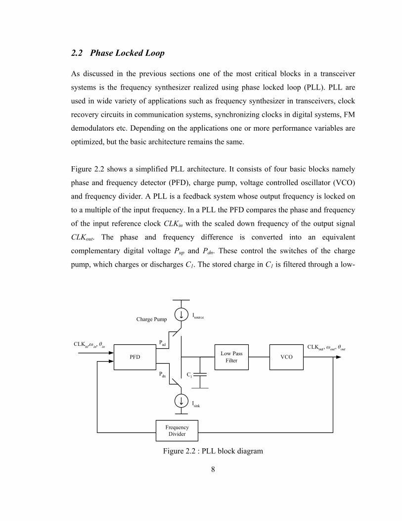
2.2 Phase Locked Loop As discussed in the previous sections one of the most critical blocks in a transceiver
systems is the frequency synthesizer realized using phase locked loop (PLL). PLL are
used in wide variety of applications such as frequency synthesizer in transceivers, clock
recovery circuits in communication systems, synchronizing clocks in digital systems, FM
demodulators etc. Depending on the applications one or more performance variables are
optimized, but the basic architecture remains the same.
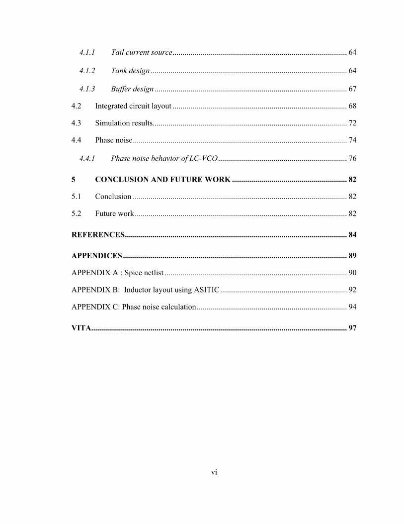
Figure 2.2 shows a simplified PLL architecture. It consists of four basic blocks namely
phase and frequency detector (PFD), charge pump, voltage controlled oscillator (VCO)
and frequency divider. A PLL is a feedback system whose output frequency is locked on
to a multiple of the input frequency. In a PLL the PFD compares the phase and frequency
of the input reference clock CLKin with the scaled down frequency of the output signal
CLKout. The phase and frequency difference is converted into an equivalent
complementary digital voltage Pup and Pdn. These control the switches of the charge
pump, which charges or discharges C1. The stored charge in C1 is filtered through a low-
CLKout, ωout, θout
PFD Low PassFilter
FrequencyDivider
VCO
Charge Pump
C1
Isource
Isink
CLKin,ωin, θinPud
Pdn
Figure 2.2 : PLL block diagram
9
pass filter and fed as control signal to the VCO. The output frequency of the VCO varies
in proportion to the control voltage. Within a few iteration the output signal locks to a
input reference clock signal. The novelty about this scheme is that the reference input
clock can be a low frequency stable crystal clock signal and output can be RF carrier
signal depending on the dividing ratio. The most critical block in terms of noise
performance is the VCO.
2.3 Types of VCO
VCO can be broadly classified into two categories; the relaxation or the non-linear
oscillators and the harmonic or the sinusoidal oscillators. Each category has its own
advantages and disadvantages. Table 2.1 summarizes the difference between the two
types.
The main applications of VCO are in communication transceivers and data
communication, as a critical component in frequency synthesizers as discussed in the
earlier section. Most of the sub-blocks except the frequency synthesizer in modern
implementations are digital blocks. In a complete integrated environment the VCO share
the same substrate with the rest of the noisy digital blocks. Hence the type of VCO
chosen for such applications should be highly immune to noise for rest of the sub-blocks
to function properly. Also the current wireless spectrum in the frequency range of
800MHz – 2.5GHz has very narrow channel spacing. Hence the reference carrier signal
from the frequency synthesizer should be a pure sinusoidal signal. With all these strict
noise requirements LC VCO becomes the best choice for wireless applications.
Non-linear oscillators which offer their own advantages such as wide tuning range and
small area find wide application in data communication, clock recovery and some low
frequency synthesizers which do not require strict noise requirements. In the current
discussion the general working of VCO and its design equation would be derived based
on general model of LC-VCO. Later a brief description of non-linear oscillators will be
presented.
10
2.4 Analysis
An electronic oscillator generates a periodic output by a self-sustaining mechanism that
allows its own noise to grow and eventually produce a stable periodic output [15]. In
other words an electronic oscillator can also be described as a system that converts dc-
power to a periodic output. There are two different topologies that describe how the noise
signal builds up to a sustained periodic output. One is a simple feedback model as shown
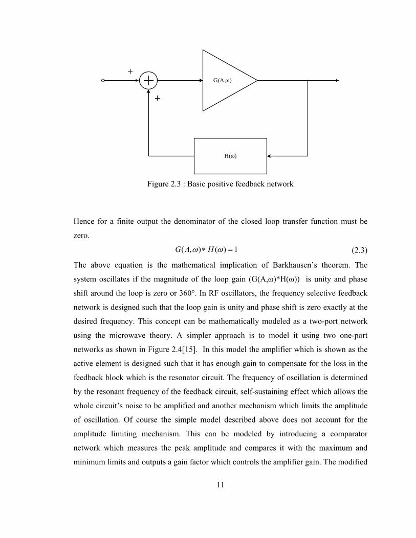
in Figure 2.3. The model has an amplifier whose frequency and amplitude dependent gain
is given by G(A,ω) and a feedback tuned circuit whose transfer function is given by
H(ω). The closed loop gain using control systems block simplification is given by
)(*),(1),(
ωωω
HAGAG
vv
i
o
−= (2.1)
where vo is the output signal. In case of oscillators, there is no input signal
0=iv (2.2)
Table 2.1: VCO comparison
Harmonic Oscillators Non- Linear Oscillators
Requires special considerations for
stabilizing the tank Simple design
Constrained by the area of passive
implementation Minimum area required
Built-in filter circuit No built-in filter circuit
Limited tuning range Wide tunabilty
Superior phase noise performance Susceptible to noise
Output frequency is susceptible to
passive device tolerance Stable output frequency
Example : LC VCO Example: Ring Oscillator
11
Hence for a finite output the denominator of the closed loop transfer function must be
zero.
1)(),( =∗ ωω HAG (2.3)
The above equation is the mathematical implication of Barkhausen’s theorem. The
system oscillates if the magnitude of the loop gain (G(A,ω)*H(ω)) is unity and phase
shift around the loop is zero or 360°. In RF oscillators, the frequency selective feedback
network is designed such that the loop gain is unity and phase shift is zero exactly at the
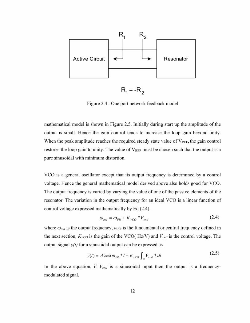
desired frequency. This concept can be mathematically modeled as a two-port network
using the microwave theory. A simpler approach is to model it using two one-port
networks as shown in Figure 2.4[15]. In this model the amplifier which is shown as the
active element is designed such that it has enough gain to compensate for the loss in the
feedback block which is the resonator circuit. The frequency of oscillation is determined
by the resonant frequency of the feedback circuit, self-sustaining effect which allows the
whole circuit’s noise to be amplified and another mechanism which limits the amplitude
of oscillation. Of course the simple model described above does not account for the
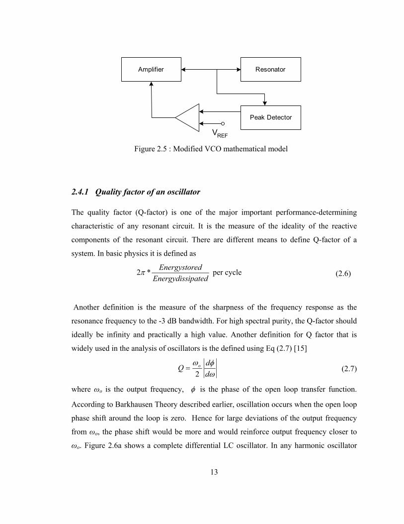
amplitude limiting mechanism. This can be modeled by introducing a comparator
network which measures the peak amplitude and compares it with the maximum and
minimum limits and outputs a gain factor which controls the amplifier gain. The modified
H(ω)
G(A,ω)
Figure 2.3 : Basic positive feedback network
12
mathematical model is shown in Figure 2.5. Initially during start up the amplitude of the
output is small. Hence the gain control tends to increase the loop gain beyond unity.
When the peak amplitude reaches the required steady state value of VREF, the gain control
restores the loop gain to unity. The value of VREF must be chosen such that the output is a
pure sinusoidal with minimum distortion.
VCO is a general oscillator except that its output frequency is determined by a control
voltage. Hence the general mathematical model derived above also holds good for VCO.
The output frequency is varied by varying the value of one of the passive elements of the
resonator. The variation in the output frequency for an ideal VCO is a linear function of
control voltage expressed mathematically by Eq (2.4).
cntlVCOFRout VK *+= ωω (2.4)
where ωout is the output frequency, ωFR is the fundamental or central frequency defined in
the next section, KVCO is the gain of the VCO( Hz/V) and Vcntl is the control voltage. The
output signal y(t) for a sinusoidal output can be expressed as
∫ ∞−+=
t
cntlVCOFR dtVKtAty **cos()( ω (2.5)
In the above equation, if Vcntl is a sinusoidal input then the output is a frequency-
modulated signal.
Active Circuit Resonator
R1 R2
R1 = -R2
Figure 2.4 : One port network feedback model
13
2.4.1 Quality factor of an oscillator The quality factor (Q-factor) is one of the major important performance-determining
characteristic of any resonant circuit. It is the measure of the ideality of the reactive
components of the resonant circuit. There are different means to define Q-factor of a
system. In basic physics it is defined as
ipatedEnergydissedEnergystor*2π per cycle (2.6)
Another definition is the measure of the sharpness of the frequency response as the
resonance frequency to the -3 dB bandwidth. For high spectral purity, the Q-factor should
ideally be infinity and practically a high value. Another definition for Q factor that is
widely used in the analysis of oscillators is the defined using Eq (2.7) [15]
ωφω
ddQ o
2= (2.7)
where ωo is the output frequency, φ is the phase of the open loop transfer function.
According to Barkhausen Theory described earlier, oscillation occurs when the open loop
phase shift around the loop is zero. Hence for large deviations of the output frequency
from ωo, the phase shift would be more and would reinforce output frequency closer to
ωo. Figure 2.6a shows a complete differential LC oscillator. In any harmonic oscillator
Amplifier Resonator
Peak Detector
VREF Figure 2.5 : Modified VCO mathematical model
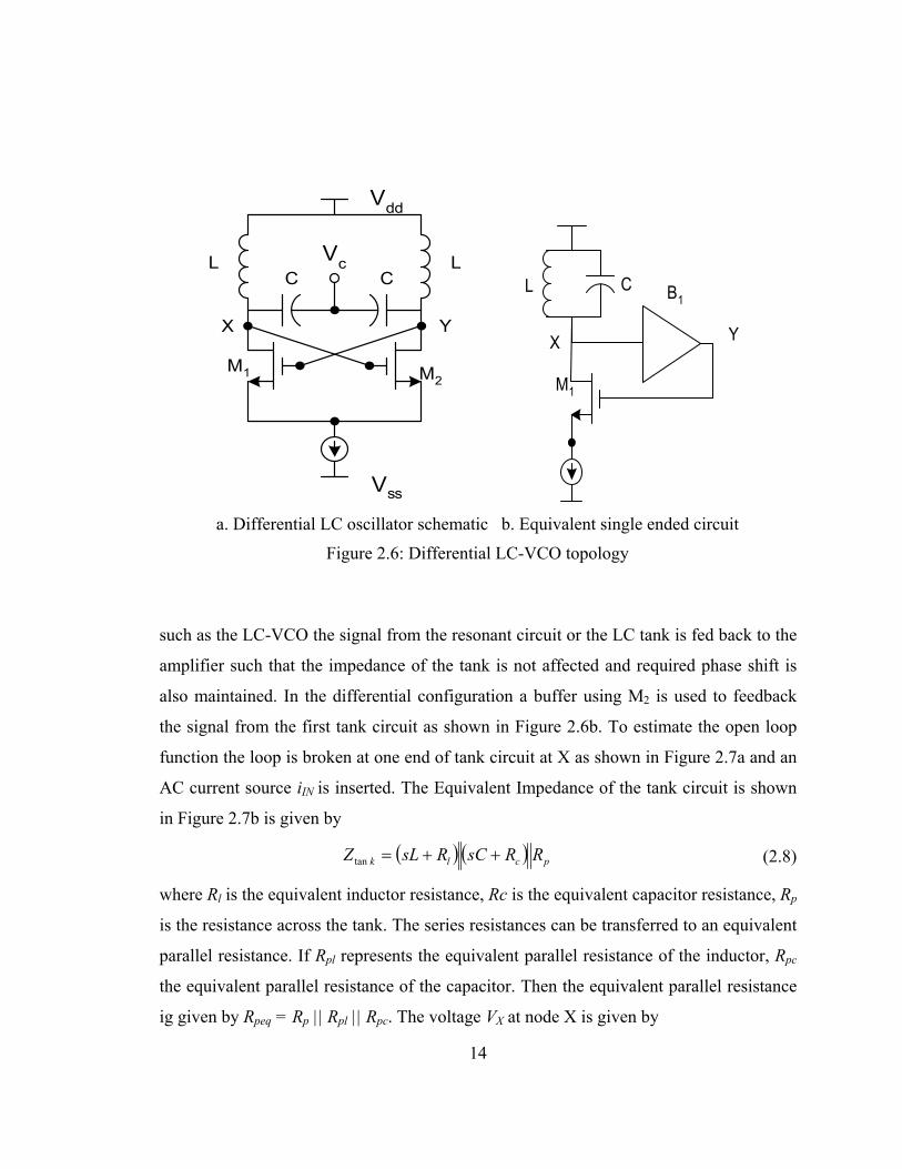
14
such as the LC-VCO the signal from the resonant circuit or the LC tank is fed back to the
amplifier such that the impedance of the tank is not affected and required phase shift is
also maintained. In the differential configuration a buffer using M2 is used to feedback
the signal from the first tank circuit as shown in Figure 2.6b. To estimate the open loop
function the loop is broken at one end of tank circuit at X as shown in Figure 2.7a and an
AC current source iIN is inserted. The Equivalent Impedance of the tank circuit is shown
in Figure 2.7b is given by
( ) ( ) pclk RRsCRsLZ ++=tan (2.8)
where Rl is the equivalent inductor resistance, Rc is the equivalent capacitor resistance, Rp
is the resistance across the tank. The series resistances can be transferred to an equivalent
parallel resistance. If Rpl represents the equivalent parallel resistance of the inductor, Rpc
the equivalent parallel resistance of the capacitor. Then the equivalent parallel resistance
ig given by Rpeq = Rp || Rpl || Rpc. The voltage VX at node X is given by
L LC C
M1 M2
Vc
Vdd
Vss
X Y
M1
X Y
L C B1
a. Differential LC oscillator schematic b. Equivalent single ended circuit
Figure 2.6: Differential LC-VCO topology
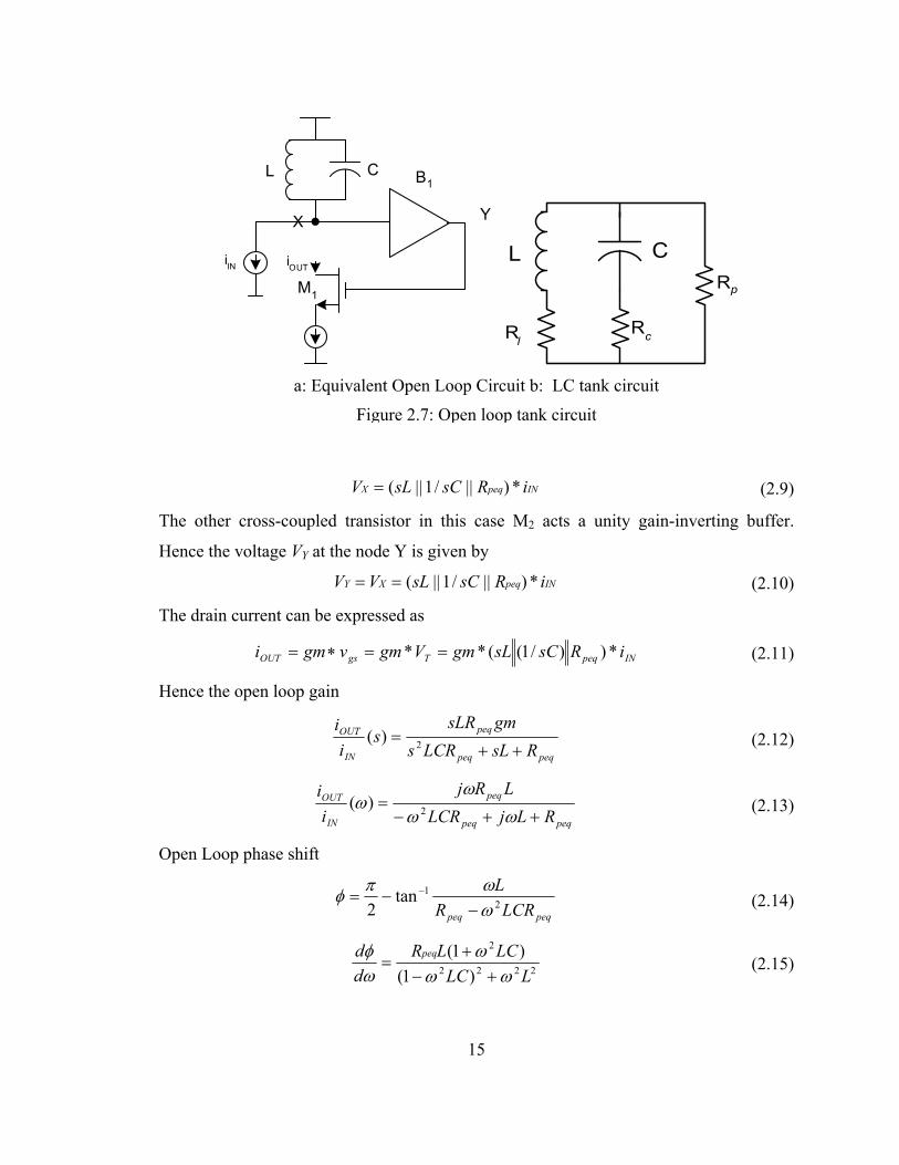
15
INpeqX iRsCsLV *)||/1||(= (2.9)
The other cross-coupled transistor in this case M2 acts a unity gain-inverting buffer.
Hence the voltage VY at the node Y is given by
INpeqXY iRsCsLVV *)||/1||(== (2.10)
The drain current can be expressed as
INpeqTgsOUT iRsCsLgmVgmvgmi *))/1((** ==∗= (2.11)
Hence the open loop gain
peqpeq
peq
IN
OUT
RsLLCRsgmsLR
si
i++
= 2)( (2.12)
peqpeq
peq
IN
OUT
RLjLCRLRj
ii
++−=
ωωω
ω 2)( (2.13)
Open Loop phase shift
peqpeq LCRRL2
1tan2 ω
ωπφ−
−= − (2.14)
2222
2
)1()1(LLC
LCLRdd peq
ωωω
ωφ
+−+
= (2.15)
M1
X Y
L C B1
iOUTiIN L C
Rl Rc
Rp
a: Equivalent Open Loop Circuit b: LC tank circuit
Figure 2.7: Open loop tank circuit
16
peqo
CRdd 2=
=ωωωφ , where the output frequency
LCo 1
=ω , Hence Q-factor can be
expressed as
ωφω
ddQ *
20=
LR
CRo
peqpeqo ω
ω == (2.16)
QLR opeq ω= (2.17)
For an ideal oscillator 1* =gmRpeq , but in real design a safety factor α ranging from 1.5-
3 is used. Hence the transconductance of the cross coupled transistors gm is given by
QLgm
oωα
= (2.18)
This is one of the key design equations for LC-VCO design.
2.5 Principle of LC oscillator Deep insight into the design of optimized LC-VCO is possible only with the firm
understanding of the trade-offs among the design parameters. This is essential to enhance
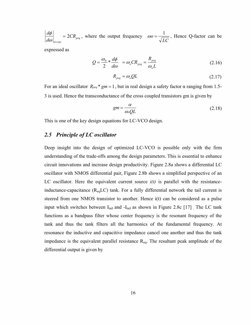
circuit innovations and increase design productivity. Figure 2.8a shows a differential LC
oscillator with NMOS differential pair, Figure 2.8b shows a simplified perspective of an
LC oscillator. Here the equivalent current source i(t) is parallel with the resistance-
inductance-capacitance (ReqLC) tank. For a fully differential network the tail current is
steered from one NMOS transistor to another. Hence i(t) can be considered as a pulse
input which switches between Itail and -Itail as shown in Figure 2.8c [17] . The LC tank
functions as a bandpass filter whose center frequency is the resonant frequency of the
tank and thus the tank filters all the harmonics of the fundamental frequency. At
resonance the inductive and capacitive impedance cancel one another and thus the tank
impedance is the equivalent parallel resistance Req. The resultant peak amplitude of the
differential output is given by
17
eqtailamp RIV ×=π4
(2.19)
At high frequencies the switching current can be closely approximated by a sinusoidal
signal due to finite switching time and limited gain and the peak amplitude can be
approximated to
eqtailamp RIV ×= (2.20)
Since the output depends only on the tail current this region of operation is referred as the
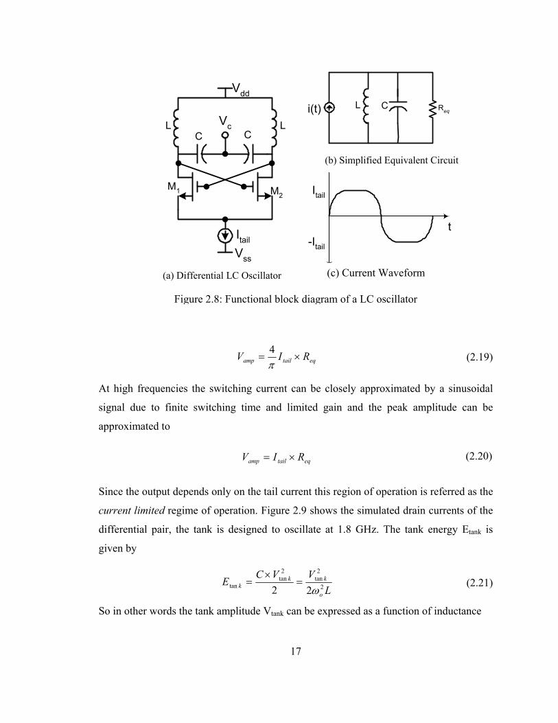
current limited regime of operation. Figure 2.9 shows the simulated drain currents of the
differential pair, the tank is designed to oscillate at 1.8 GHz. The tank energy Etank is
given by
LVVC
Eo
kkk 2
2tan
2tan
tan 22 ω=
×= (2.21)
So in other words the tank amplitude Vtank can be expressed as a function of inductance
L LC C
M1 M2
Vc
Vdd
Vss
Itail
L C Reqi(t)
i(t)
Itail
-Itail
t
Figure 2.8: Functional block diagram of a LC oscillator
(a) Differential LC Oscillator
(b) Simplified Equivalent Circuit
(c) Current Waveform
18
LEV kk tan0tan 2ω= (2.22)
The tank amplitude grows with the independent variable inductance L when all other
variables are kept constant and hence this mode of operation is also referred as
inductance – limited mode. Any equation valid in the current limited mode is also valid in
inductance limited mode. Vtank grows with the bias current built-up or inductance until it
reaches a saturated limiting voltage Vlimit close to the supply voltage, this region is
referred as voltage limited mode of operation. In this mode the PMOS transistor (current
source) enters the triode region and the drain current does not stay constant and hence
there is a huge drop in the VDS in the differential pair.
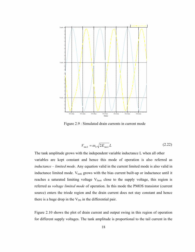
Figure 2.10 shows the plot of drain current and output swing in this region of operation
for different supply voltages. The tank amplitude is proportional to the tail current in the
Figure 2.9 : Simulated drain currents in current mode
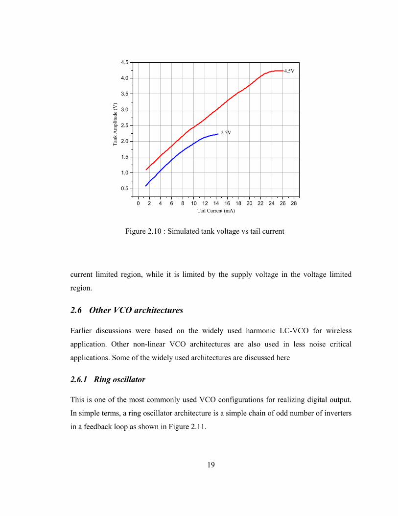
19
current limited region, while it is limited by the supply voltage in the voltage limited
region.
2.6 Other VCO architectures Earlier discussions were based on the widely used harmonic LC-VCO for wireless
application. Other non-linear VCO architectures are also used in less noise critical
applications. Some of the widely used architectures are discussed here
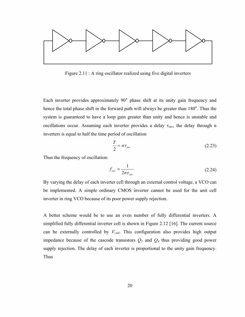
2.6.1 Ring oscillator This is one of the most commonly used VCO configurations for realizing digital output.
In simple terms, a ring oscillator architecture is a simple chain of odd number of inverters
in a feedback loop as shown in Figure 2.11.
0 2 4 6 8 10 12 14 16 18 20 22 24 26 28
0.5
1.0
1.5
2.0
2.5
3.0
3.5
4.0
4.5
Tank
Am
plitu
de (V
)
Tail Current (mA)
2.5V
4.5V
Figure 2.10 : Simulated tank voltage vs tail current
20
Each inverter provides approximately 90° phase shift at its unity gain frequency and
hence the total phase shift in the forward path will always be greater than 180°. Thus the
system is guaranteed to have a loop gain greater than unity and hence is unstable and
oscillations occur. Assuming each inverter provides a delay τinv, the delay through n
inverters is equal to half the time period of oscillation
invnT τ=2
(2.23)
Thus the frequency of oscillation:
invosc n
fτ21
= (2.24)
By varying the delay of each inverter cell through an external control voltage, a VCO can
be implemented. A simple ordinary CMOS inverter cannot be used for the unit cell
inverter in ring VCO because of its poor power supply rejection.
A better scheme would be to use an even number of fully differential inverters. A
simplified fully differential inverter cell is shown in Figure 2.12 [16]. The current source
can be externally controlled by Vcntl. This configuration also provides high output
impedance because of the cascode transistors Q3 and Q4 thus providing good power
supply rejection. The delay of each inverter is proportional to the unity gain frequency.
Thus
Figure 2.11 : A ring oscillator realized using five digital inverters
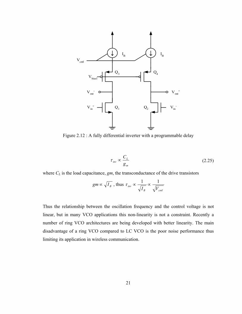
21
m
Linv g
C∝τ (2.25)
where CL is the load capacitance, gm, the transconductance of the drive transistors
BIgm ∝ , thus cntlB
inv VI11
∝∝τ
Thus the relationship between the oscillation frequency and the control voltage is not
linear, but in many VCO applications this non-linearity is not a constraint. Recently a
number of ring VCO architectures are being developed with better linearity. The main
disadvantage of a ring VCO compared to LC VCO is the poor noise performance thus
limiting its application in wireless communication.
IB IB
Q3 Q4
Q2Q1
Vout+Vout
-
Vin+ Vin
-
Vbias1
Vcntl
Figure 2.12 : A fully differential inverter with a programmable delay
22
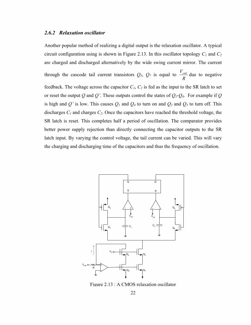
2.6.2 Relaxation oscillator Another popular method of realizing a digital output is the relaxation oscillator. A typical
circuit configuration using is shown in Figure 2.13. In this oscillator topology C1 and C2
are charged and discharged alternatively by the wide swing current mirror. The current
through the cascode tail current transistors Q5, Q7 is equal to R
Vcntl due to negative
feedback. The voltage across the capacitor C1, C2 is fed as the input to the SR latch to set
or reset the output Q and Q’. These outputs control the states of Q1-Q4. For example if Q
is high and Q’ is low. This causes Q1 and Q4 to turn on and Q2 and Q3 to turn off. This
discharges C1 and charges C2. Once the capacitors have reached the threshold voltage, the
SR latch is reset. This completes half a period of oscillation. The comparator provides
better power supply rejection than directly connecting the capacitor outputs to the SR
latch input. By varying the control voltage, the tail current can be varied. This will vary
the charging and discharging time of the capacitors and thus the frequency of oscillation.
Q6 Q5
Q7Q8
Vb
RVcntl
I
+
-
Q1
Q3 Q4
Q2
C2
Vref
+ -+-
Vref
C1
S R
Q’Q
Figure 2.13 : A CMOS relaxation oscillator
23
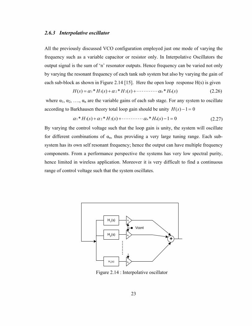
2.6.3 Interpolative oscillator
All the previously discussed VCO configuration employed just one mode of varying the
frequency such as a variable capacitor or resistor only. In Interpolative Oscillators the
output signal is the sum of ‘n’ resonator outputs. Hence frequency can be varied not only
by varying the resonant frequency of each tank sub system but also by varying the gain of
each sub-block as shown in Figure 2.14 [15]. Here the open loop response H(s) is given
)(*)(*)(*)( 2211 sHsHsHsH nnααα ⋅⋅⋅⋅⋅⋅⋅⋅⋅⋅⋅⋅++= (2.26)
where α1, α2, …., αn are the variable gains of each sub stage. For any system to oscillate
according to Barkhausen theory total loop gain should be unity 01)( =−sH
01)(*)(*)(* 2211 =−⋅⋅⋅⋅⋅⋅⋅⋅⋅⋅⋅⋅++ sHsHsH nnααα (2.27)
By varying the control voltage such that the loop gain is unity, the system will oscillate
for different combinations of αn, thus providing a very large tuning range. Each sub-
system has its own self resonant frequency; hence the output can have multiple frequency
components. From a performance perspective the systems has very low spectral purity,
hence limited in wireless application. Moreover it is very difficult to find a continuous
range of control voltage such that the system oscillates.
H1(s)
H2(s)
Hn(s)
+
Vcont
α1
α2
αn
Figure 2.14 : Interpolative oscillator
24
3 INTEGRATED INDUCTORS AND VARACTORS Phase Locked Loops (PLL) are widely used as frequency synthesizers, clock and data
recovery circuits and carrier synchronization circuits in wireless application. Effective
performance of PLL for these applications depends extensively on the implementation of
the most critical component voltage controlled oscillator (VCO). Of the various
implementations of VCO discussed in the earlier sections LC-VCO is the best choice in
terms of noise performance. The major constraint in the implementation of integrated
wireless communication device in silicon is the development of an integrated inductor as
well as the high Q-factor varactor.
In this chapter, various means of realizing integrated inductors have been explored and
finally, the most viable implementation of the spiral inductors in terms cost, high
frequency of operation and repeatability has been elaborately analyzed. Different means
of developing varactors in standard CMOS technology have been studied and a new
novel scheme of using MOS transistors in accumulation mode body driven varactor has
been presented. A simplified equivalent circuit for the body driven varactor has also been
developed.
3.1 Importance of integrated inductor As discussed in Chapter 1, there is a great need to develop a completely integrated
transceiver system. The frequency limit used for commercial application is increasing
everyday. As the desired frequency of operation increases the values of the inductance
and the varactor capacitance decreases. Table 3.1 gives a general overview of the
frequency of operation and the required inductance. Figure 3.1 [18] shows the different
parasitic inductance associated with the bondpad and the package. The total effective
inductance is the sum of the off-chip inductance and the parasitic inductance given by Eq
(3.1)
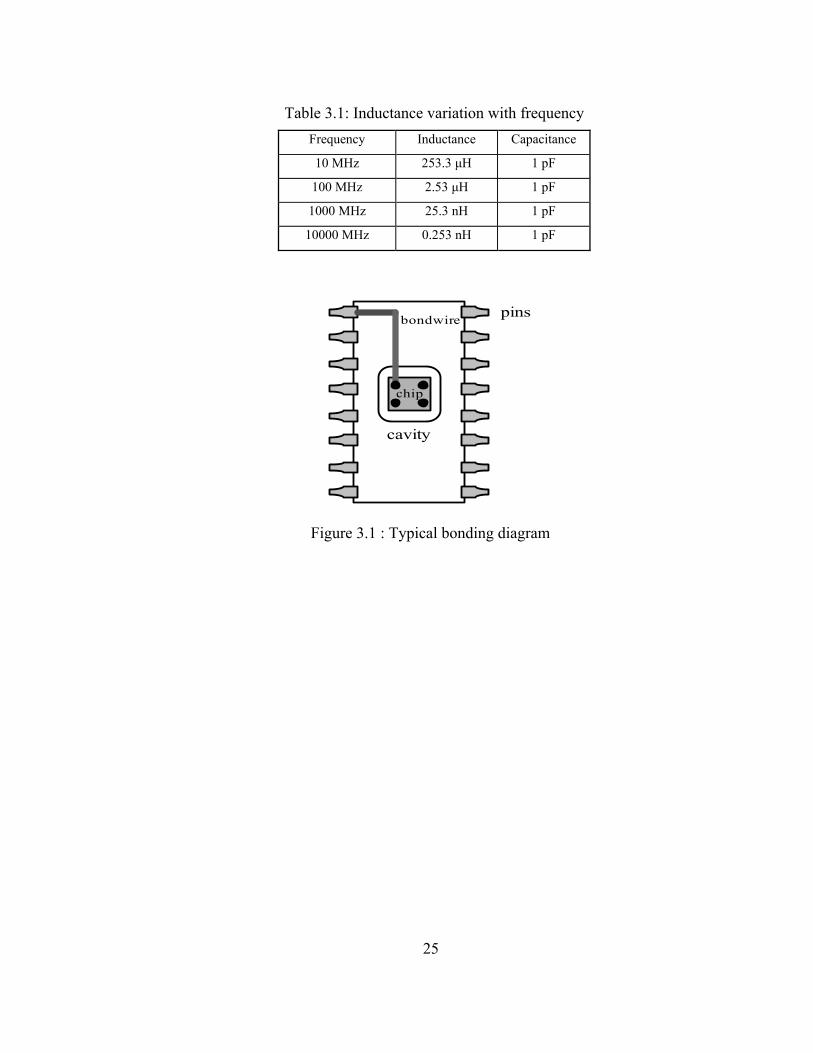
25
chip
cavity
bondwire pins
Figure 3.1 : Typical bonding diagram
Table 3.1: Inductance variation with frequency Frequency Inductance Capacitance
10 MHz 253.3 µH 1 pF
100 MHz 2.53 µH 1 pF
1000 MHz 25.3 nH 1 pF
10000 MHz 0.253 nH 1 pF
26
bondwirepinoffchipeff LLLL ++= (3.1)
The bondwire inductance usually varies between 4.5 nH – 2.95 nH [19] depending on the
package. The package inductance is usually around 0.5 nH. These parasitic effects are
negligible at low RF frequencies. But at high frequencies around of 1 GHz the parasitic
inductance becomes a substantial percentage of the total effective inductance. This
reduces the performance of the effective inductor since substantial part of the effective
inductance is contributed by the low Q-factor parasitic inductance. Thus although off-
chip inductors can be used at around 1 GHz, the performance of these inductors are
deteriorated. The problem is worse at higher frequencies of around 10 GHz, where the
effective inductance required is only 0.253 nH for 1pF capacitance. Such a low value of
inductance cannot be realized externally even with the best tiny package. Thus there
arises a need for pondering new means of realizing integrated for wireless applications.
3.2 Integrated inductor design
The successful implementation of the LC VCO oscillator depends extensively on the
performance of high Q integrated inductors. In the past the electronic circuits using
inductors were rarely used due to their bulky and noisy nature. But in the current
revolution for wireless communication products which require high spectral quality
carrier signals which as per discussions in the earlier chapter points to the use LC VCO.
Hence a lot of work is currently being pursued to build area efficient high performance
inductors integrated with other transceiver circuits in a single die. The main constraint in
this approach is the unavailability of standard modeled inductors in standard CMOS
process. Currently there exist the following methods to implement integrated inductors:
27
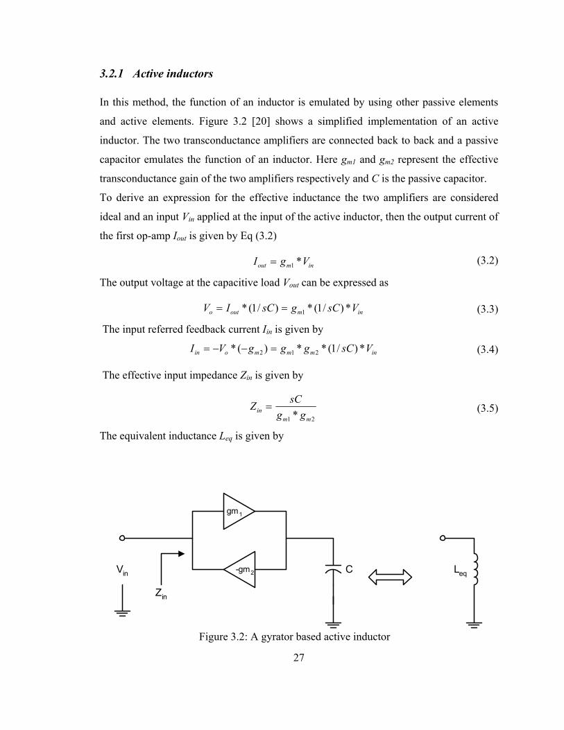
3.2.1 Active inductors In this method, the function of an inductor is emulated by using other passive elements
and active elements. Figure 3.2 [20] shows a simplified implementation of an active
inductor. The two transconductance amplifiers are connected back to back and a passive
capacitor emulates the function of an inductor. Here gm1 and gm2 represent the effective
transconductance gain of the two amplifiers respectively and C is the passive capacitor.
To derive an expression for the effective inductance the two amplifiers are considered
ideal and an input Vin applied at the input of the active inductor, then the output current of
the first op-amp Iout is given by Eq (3.2)
inmout VgI *1= (3.2)
The output voltage at the capacitive load Vout can be expressed as
inmouto VsCgsCIV *)/1(*)/1(* 1== (3.3)
The input referred feedback current Iin is given by
inmmmoin VsCgggVI *)/1(**)(* 212 =−−= (3.4)
The effective input impedance Zin is given by
21 * mmin gg
sCZ = (3.5)
The equivalent inductance Leq is given by
gm1
-gm2 CVin
Zin
Leq
Figure 3.2: A gyrator based active inductor
28
21 * mmeq gg
CL = (3.6)
The resonant frequency of the tank circuit can be varied by controlling the
transconductance gain gm1 and gm2. This provides very large tuning range, which is the
main advantage of this implementation. Moreover this type of inductor implementation
offers other advantages like small area and simple implementation.
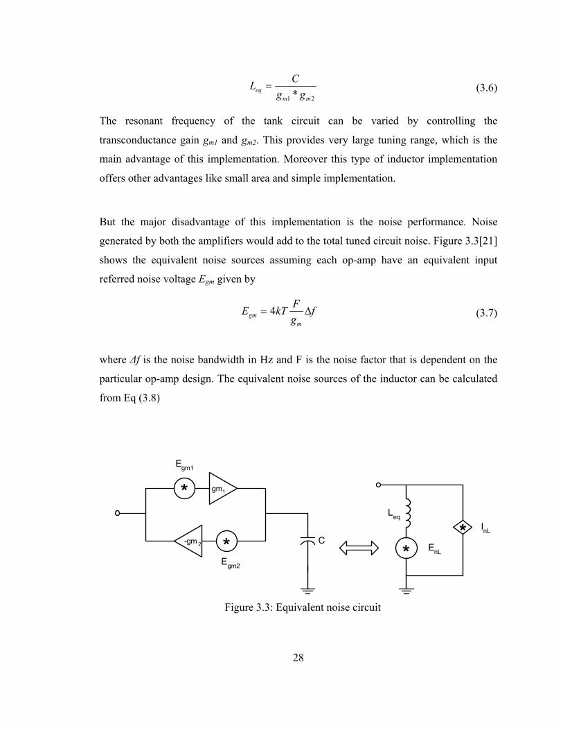
But the major disadvantage of this implementation is the noise performance. Noise
generated by both the amplifiers would add to the total tuned circuit noise. Figure 3.3[21]
shows the equivalent noise sources assuming each op-amp have an equivalent input
referred noise voltage Egm given by
fgFkTE
mgm ∆= 4 (3.7)
where ∆f is the noise bandwidth in Hz and F is the noise factor that is dependent on the
particular op-amp design. The equivalent noise sources of the inductor can be calculated
from Eq (3.8)
gm1
-gm 2 C
Leq
*
*
Egm1
Egm2* EnL
* InL
Figure 3.3: Equivalent noise circuit
29
fgF
kTEEm
gmgmnL ∆==
1
121
2 4 (3.8)
fgkTFEgI mgmgmmnL ∆== 222
22
22 4 (3.9)
Eq (3.8) and Eq (3.9) shows that the both the transconductance amplifier equivalent noise
source contribute to the total inductor noise. The main purpose of using a LC-VCO in
GHz range is to obtain carrier signals of high spectral purity. Even though active
inductors offer wide tunabilty, this is inadequate for wireless applications.
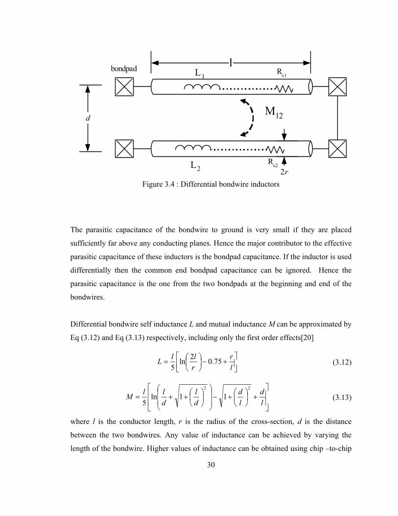
3.2.2 Bondwire inductors
Another method of implementing an integrated inductor is to use the parasitic inductance
of the bonding wire in an IC package. Figure 3.4 [20] shows a typical cross-section of the
differential bondwire inductor. The inductance can be roughly calculated as 1nH per mm.
Usually gold or aluminum are used as bondwire in standard IC package. The series
resistance per unit length is given by
ARseries
ρ= (3.10)
where ρ ,the resistivity of the wire is related to skin depth δ and permeability µ is given
2
2ωµδρ = (3.11)
For a 1mm Al or Au at 1GHz, the skin depth is approximately 2.5µm which is relatively
small compared to the typical radius of the bondwire (25 µm). Hence the area of the cross
section A can be approximated as rπ2 . Substituting the values of permeability of Au for
1 GHz frequency the series resistance can be approximated as 125 mΩ per mm length
[20]. Since the bondwire inductors have very low series resistance, or stated differently
from a designers perspective, they have very high Q-factor of around 200, a very
desirable characteristic of any resonant circuit.
30
The parasitic capacitance of the bondwire to ground is very small if they are placed
sufficiently far above any conducting planes. Hence the major contributor to the effective
parasitic capacitance of these inductors is the bondpad capacitance. If the inductor is used
differentially then the common end bondpad capacitance can be ignored. Hence the
parasitic capacitance is the one from the two bondpads at the beginning and end of the
bondwires.
Differential bondwire self inductance L and mutual inductance M can be approximated by
Eq (3.12) and Eq (3.13) respectively, including only the first order effects[20]
+−
=
lr
rllL 75.02ln
5 (3.12)
+
+−
++=
ld
ld
dl
dllM
22
11ln5
(3.13)
where l is the conductor length, r is the radius of the cross-section, d is the distance
between the two bondwires. Any value of inductance can be achieved by varying the
length of the bondwire. Higher values of inductance can be obtained using chip –to-chip
L1Rs1
L2Rs2
M12
bondpad
2r
l
d
Figure 3.4 : Differential bondwire inductors
31
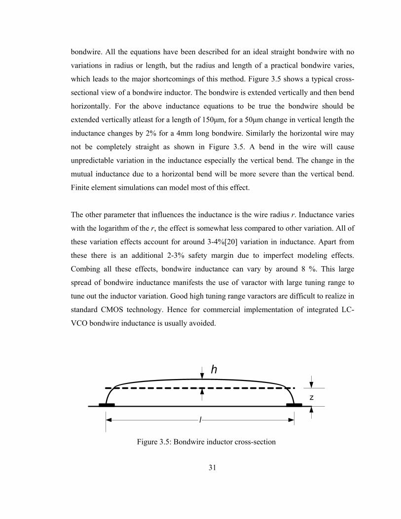
bondwire. All the equations have been described for an ideal straight bondwire with no
variations in radius or length, but the radius and length of a practical bondwire varies,
which leads to the major shortcomings of this method. Figure 3.5 shows a typical cross-
sectional view of a bondwire inductor. The bondwire is extended vertically and then bend
horizontally. For the above inductance equations to be true the bondwire should be
extended vertically atleast for a length of 150µm, for a 50µm change in vertical length the
inductance changes by 2% for a 4mm long bondwire. Similarly the horizontal wire may
not be completely straight as shown in Figure 3.5. A bend in the wire will cause
unpredictable variation in the inductance especially the vertical bend. The change in the
mutual inductance due to a horizontal bend will be more severe than the vertical bend.
Finite element simulations can model most of this effect.
The other parameter that influences the inductance is the wire radius r. Inductance varies
with the logarithm of the r, the effect is somewhat less compared to other variation. All of
these variation effects account for around 3-4%[20] variation in inductance. Apart from
these there is an additional 2-3% safety margin due to imperfect modeling effects.
Combing all these effects, bondwire inductance can vary by around 8 %. This large
spread of bondwire inductance manifests the use of varactor with large tuning range to
tune out the inductor variation. Good high tuning range varactors are difficult to realize in
standard CMOS technology. Hence for commercial implementation of integrated LC-
VCO bondwire inductance is usually avoided.
h
l
z
Figure 3.5: Bondwire inductor cross-section
32
3.2.3 Inductor on a package
Another method of integrating inductors is through thin film multi chip module
technology (MCM) to connect multiple chips. The individual sub-RF blocks can now be
implemented in the most suitable IC technology and can be eventually assembled in a
relatively simple and economical way. An optimal partitioning of the system into the sub-
blocks will lead to lower cost, increase of manufacturing yield and superior performance.
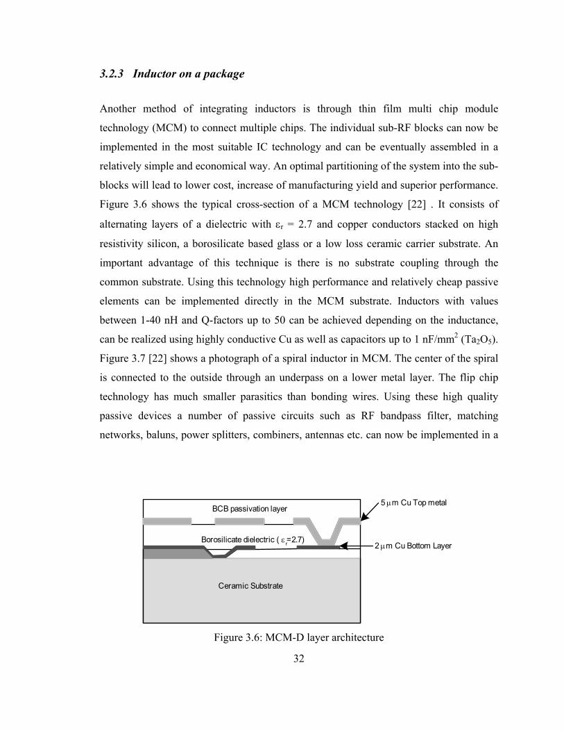
Figure 3.6 shows the typical cross-section of a MCM technology [22] . It consists of
alternating layers of a dielectric with εr = 2.7 and copper conductors stacked on high
resistivity silicon, a borosilicate based glass or a low loss ceramic carrier substrate. An
important advantage of this technique is there is no substrate coupling through the
common substrate. Using this technology high performance and relatively cheap passive
elements can be implemented directly in the MCM substrate. Inductors with values
between 1-40 nH and Q-factors up to 50 can be achieved depending on the inductance,
can be realized using highly conductive Cu as well as capacitors up to 1 nF/mm2 (Ta2O5).
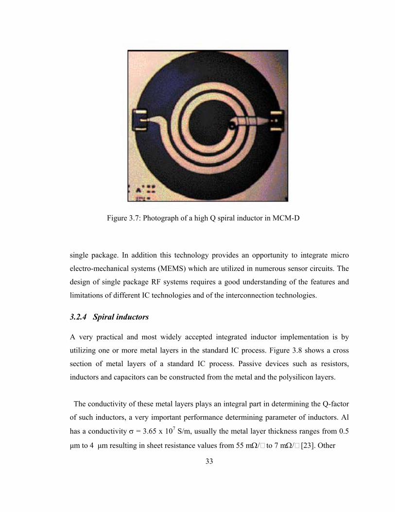
Figure 3.7 [22] shows a photograph of a spiral inductor in MCM. The center of the spiral
is connected to the outside through an underpass on a lower metal layer. The flip chip
technology has much smaller parasitics than bonding wires. Using these high quality
passive devices a number of passive circuits such as RF bandpass filter, matching
networks, baluns, power splitters, combiners, antennas etc. can now be implemented in a
BCB passivation layer5 µm Cu Top metal
2 µm Cu Bottom LayerBorosilicate dielectric ( ε r=2.7)
Ceramic Substrate
Figure 3.6: MCM-D layer architecture
33
single package. In addition this technology provides an opportunity to integrate micro
electro-mechanical systems (MEMS) which are utilized in numerous sensor circuits. The
design of single package RF systems requires a good understanding of the features and
limitations of different IC technologies and of the interconnection technologies.
3.2.4 Spiral inductors A very practical and most widely accepted integrated inductor implementation is by
utilizing one or more metal layers in the standard IC process. Figure 3.8 shows a cross
section of metal layers of a standard IC process. Passive devices such as resistors,
inductors and capacitors can be constructed from the metal and the polysilicon layers.
The conductivity of these metal layers plays an integral part in determining the Q-factor
of such inductors, a very important performance determining parameter of inductors. Al
has a conductivity σ = 3.65 x 10⁷ S/m, usually the metal layer thickness ranges from 0.5
µm to 4 µm resulting in sheet resistance values from 55 mΩ/ to 7 mΩ/ [23]. Other
Figure 3.7: Photograph of a high Q spiral inductor in MCM-D
34
metals like Au, Ag, Cu have a lower sheet resistance than aluminum, but currently only
aluminum is compatible with the standard IC process. A lot of research is currently being
pursued to utilize the lower sheet resistance of Cu for better metal interconnect, the
success of this research would further improve the performance of Si planar on-chip
inductors. Each metal layer of different conductivity is fabricated by various processes
such as diffusion, chemical vapor deposition and growth, epitaxy and ion implantation.
The metal composition is slightly varied by mixing Al with other metals such as
platinum, palladium, titanium and tungsten to overcome some of the limitations of Al like
spiking, junction penetration etc. Electromigration in Al is another limitation, setting an
upper bound on the maximum current density. This limits the application of Si integrated
IC using on-chip inductors for high power applications like power amplifiers. For such
applications the necessary metal width requires large areas resulting in lower self
resonant frequencies limiting the application frequency. In some modern CMOS
technology a thick top metal layer is used for high-speed digital blocks for reducing clock
line delays. This top layer can be utilized for fabricating high quality spiral inductors with
very low resistive losses and thus achieve high Q-factor. This top thick metal in many IC
process resides on the top of an extra thick insulator for minimum substrate capacitance.
The option of so many metal layers along with the interconnections results in wide
varieties of inductors with no special IC processing steps in modern CMOS process.
Field Oxide
Metal4
Metal3
Metal2
Metal1
poly
Epitaxial Layer
Substrate Layer
Figure 3.8: Cross-section of typical CMOS substrate layer
35
3.3 Loss mechanism of on-chip inductor
In order to design the optimum inductor for a particular application, an insight into the
various losses of the planar spiral inductor is necessary. For any inductor structure the
change in the current distribution causes many undesirable effects such as skin effect,
current constriction and current crowding. The alternating electric current always takes
the path of the lowest impedance. The current tends to accumulate in the outer layer since
magnetic field of the inductor produces opposing electric field. This opposing field
follows a f dependence. The AC resistance increases with opposing field and this
effect is known as skin effect. At high frequencies the effective cross-sectional area of the
conductors decreases, thus increasing the current density. This causes more electric
energy being lost as heat. At high frequencies the skin effect is expressed as depth of
penetration δ given by Eq (3.14).
ωµσδ 2
= (3.14)
where µ is the permeability and σ is the conductivity. The depth of penetration varies
inversely with square root of frequency.
The above discussion considered the effect of a single metal layer. In a multi conductor
system such as fully differential LC VCO, proximity effects due to mutual magnetic
field affects the self inductance. If the coupling magnetic field adds to the self induced
magnetic field, then the AC resistance increases.
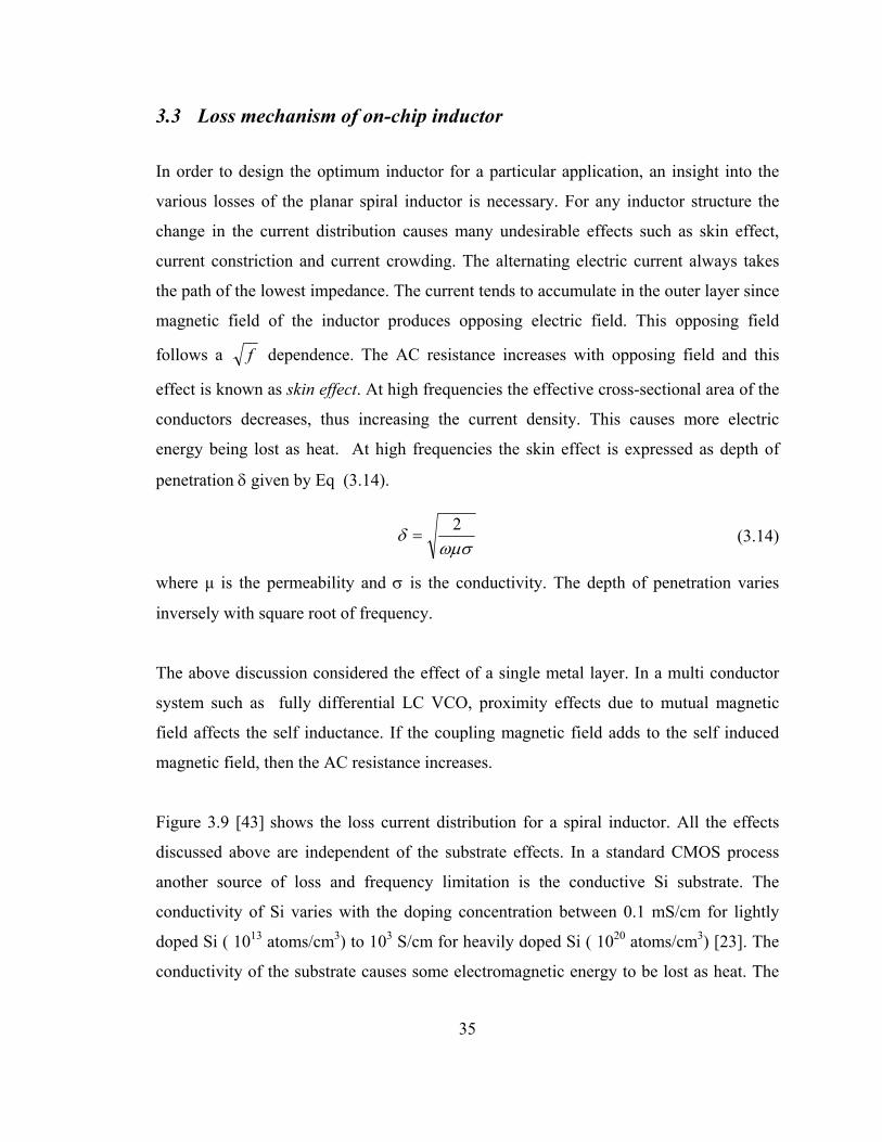
Figure 3.9 [43] shows the loss current distribution for a spiral inductor. All the effects
discussed above are independent of the substrate effects. In a standard CMOS process
another source of loss and frequency limitation is the conductive Si substrate. The
conductivity of Si varies with the doping concentration between 0.1 mS/cm for lightly
doped Si ( 1013 atoms/cm3) to 103 S/cm for heavily doped Si ( 1020 atoms/cm3) [23]. The
conductivity of the substrate causes some electromagnetic energy to be lost as heat. The
36
electric energy loss appears as a displacement current that flows through the substrate to
nearby grounds. Another form of substrate loss is due to the time varying solenoidal
electric field produced by the magnetic field. This electric field induces substrate currents
perpendicular to the spiral segments. At high frequencies electromagnetically induced
losses result when the physical dimensions of the devices approach the wavelength of
propagation. This loss is very negligible even at 100 GHz frequency since the wavelength
(3mm) becomes larger than the device dimension (submicron). Electromagnetic
propagation into the substrate occurs at lower frequencies due to the lower propagation
nature of Si and the wave propagation behaves like a “quasi- TEM” mode. The
propagation speed is proportional to Siε , slightly lower than the propagation in free
space
.
Figure 3.9: Loss current distribution of a spiral inductor
37
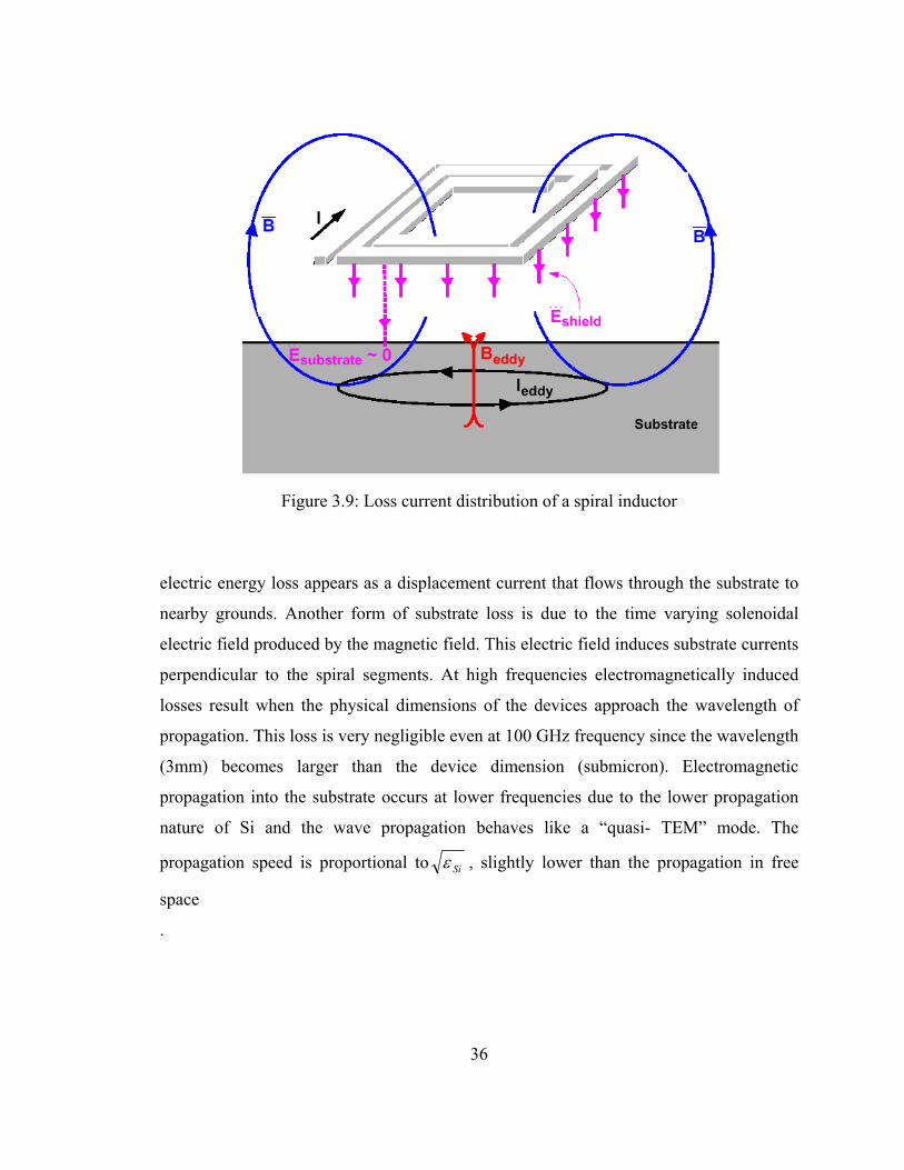
3.4 On-chip spiral inductor modeling
The behavior of spiral inductors have been modeled in several ways [24][25] [26] .
Figure 3.10 shows one of the most tangible model widely employed. It is composed of
an ideal inductor L in series with the series resistance of the spiral Rs, which is a
frequency dependent parameter. The substrate loss is modeled as a lumped coupling
capacitor Cox1 and Cox2 at the two ends in series with the substrate resistance RSUB1 and
RSUB2 which are also frequency dependent resistances. The structure of most spiral
inductors configuration is not symmetric, and hence their geometric center and the
electric center are slightly different. Hence the parasitic coupling substrate capacitances
at the two end terminals vary slightly. The difference however is very small and the two
capacitors are assumed to be the same for most geometrically symmetrical structures. Cp
represents the coupling capacitance between the two terminals due to fringing fields in
both the dielectric region and the air region. A capacitive split between Csub1 and Csub2
models the capacitance across the substrate. To simplify the equivalent model the
coupling capacitor Cp and the substrate capacitance are neglected. This is valid since the
related capacitance is very small and the inductor is operated at frequencies well below
L
Port 1 Port 2
Cp
Rs
Cox1 Cox2
Rsub1
Csub1
Csub2Rsub2
Figure 3.10 : Equivalent model of a spiral inductor
38
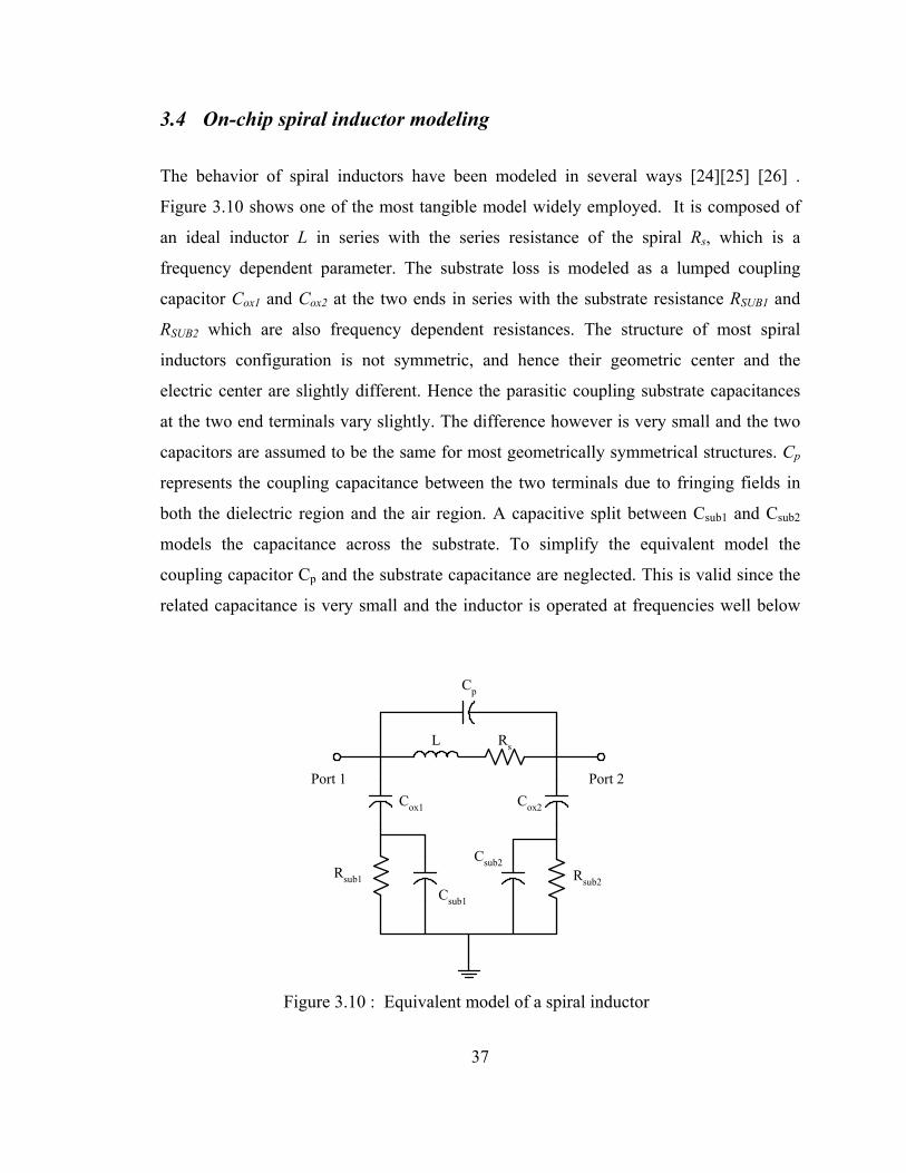
its self-resonant frequency. Hence the model shown in Figure 3.11 is a valid simplified
model for the spiral inductor.
A lot of work has been done to derive an accurate formula for the inductance of a spiral
inductor. Greenhouse [24] provides an empirical formula, which differs, from the
experimental results by less than 10%. This was further proved by Nguyen et al.[28] .
Further Remak and Burdick have derived formulas for calculating the inductance of a
circular spiral, which differs from the actual measurements by less than 8%. Figure 3.12
shows the inductance variation with number of turns and outer dimension for a square
spiral with width W=18 µm, and spacing between the metal lines S=3 µm. Eq (3.15) [29]
provides a general empirical formula for inductance.
( )nlL 19.005.1 += (3.15)
( )21
2027.1 RRWS
l o −+
=π
(3.16)
LPort 1 Port 2
Rs
Cox1 Cox2
Rsub1 Rsub2
Figure 3.11 : Simplified model of a spiral inductor
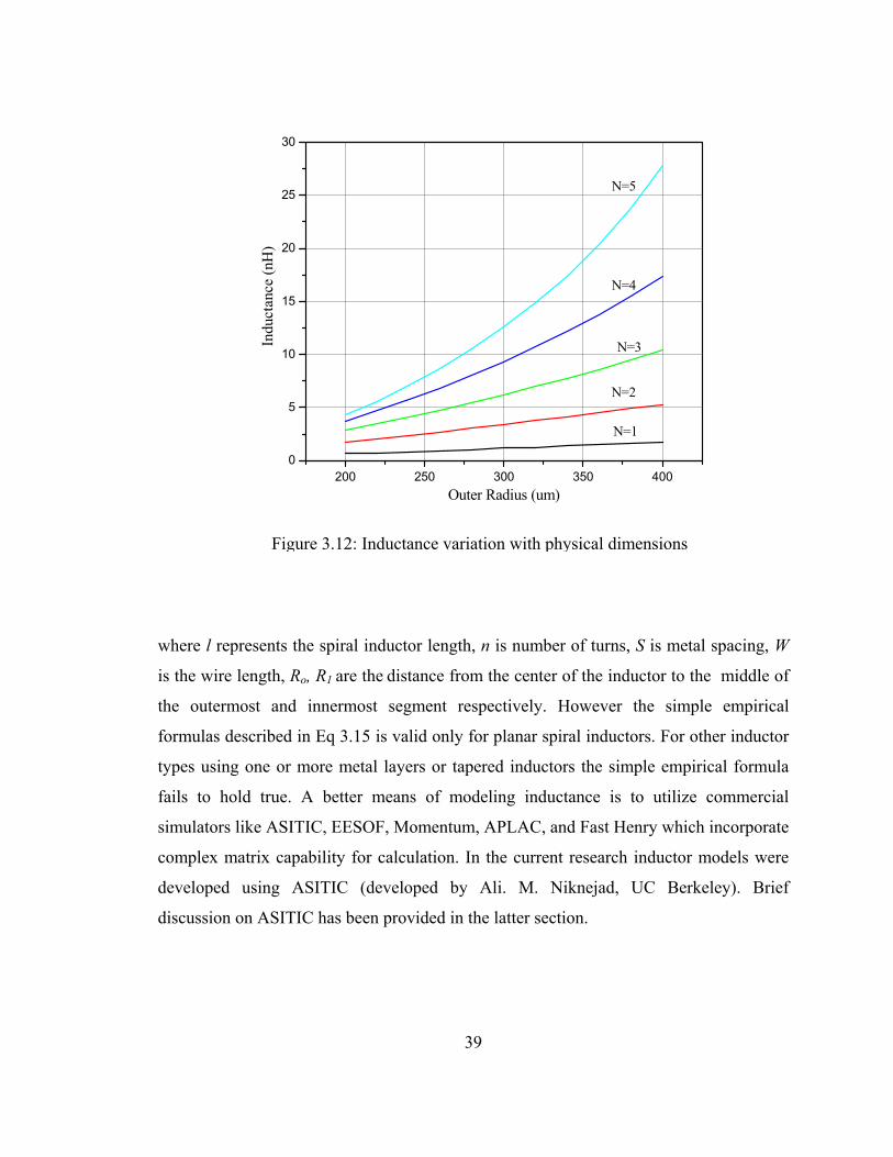
39
where l represents the spiral inductor length, n is number of turns, S is metal spacing, W
is the wire length, Ro, R1 are the distance from the center of the inductor to the middle of
the outermost and innermost segment respectively. However the simple empirical
formulas described in Eq 3.15 is valid only for planar spiral inductors. For other inductor
types using one or more metal layers or tapered inductors the simple empirical formula
fails to hold true. A better means of modeling inductance is to utilize commercial
simulators like ASITIC, EESOF, Momentum, APLAC, and Fast Henry which incorporate
complex matrix capability for calculation. In the current research inductor models were
developed using ASITIC (developed by Ali. M. Niknejad, UC Berkeley). Brief
discussion on ASITIC has been provided in the latter section.
200 250 300 350 4000
5
10
15
20
25
30
N=5
N=4
N=3
N=1
Indu
ctan
ce (n
H)
Outer Radius (um)
N=2
Figure 3.12: Inductance variation with physical dimensions
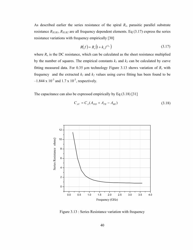
40
As described earlier the series resistance of the spiral Rs, parasitic parallel substrate
resistance RSUB1, RSUB2 are all frequency dependent elements. Eq (3.17) express the series
resistance variations with frequency empirically [30]
( ) ( )211 k
o fkRfR += (3.17)
where Ro is the DC resistance, which can be calculated as the sheet resistance multiplied
by the number of squares. The empirical constants k1 and k2 can be calculated by curve
fitting measured data. For 0.35 µm technology Figure 3.13 shows variation of Rs with
frequency and the extracted k1 and k2 values using curve fitting has been found to be
–1.844 x 10⁻³ and 1.7 x 10⁻³, respectively.
The capacitance can also be expressed empirically by Eq (3.18) [31]
)( BRFRINDAAV AAACC −+= (3.18)
0.0 0.5 1.0 1.5 2.0 2.5 3.0 3.5 4.0
0
2
4
6
8
10
12
Serie
s Res
ista
nce
ohm
s)
Frequency (GHz)
Figure 3.13 : Series Resistance variation with frequency
41
2/21 AVoxox CCC ≅≅ (3.19)
where CAV represents the capacitance of a vertical inductor area seen from the substrate,
CA is parallel plate capacitance per unit area between the inductor layer and the substrate,
AIND is the area of the spiral inductor cover, AFRI is the area corresponding to the additive
fringing contributions ( approx. 3.5 µm x total perimeter) of the spiral inductor Similarly
the substrate resistance can also be expressed empirically.
All these parasitic effects can be represented by a single design parameter, the Q-factor.
The Q-factor is directly proportional to parallel resistance and inversely proportional to
series resistance. In a multi-layer spiral inductor structure the interconnect resistance also
adds on to the series resistance. The series resistance decreases with increase in metal
width and multi-layer routing [32][33] . However these concepts are not the solution to
achieve optimum Q-factor in the frequency range of interest because of high frequency
magnetic field effects such as the skin effect [30] . As discussed earlier the skin effect
causes the resistance of a metal line of wider metal width to increase with frequency
faster than a narrower metal line. Figure 3.14 shows the variation in the Q factor with
metal width. Another important design requirement is to achieve maximum inductance
for a given area. In this perspective rectangular spiral provide the minimum inductance.
and circular spiral provides the maximum inductance for the same area. In some process
technology non-Manhattan shapes are not allowed. In such situations octagonal spiral
would be the optimum inductor shape.
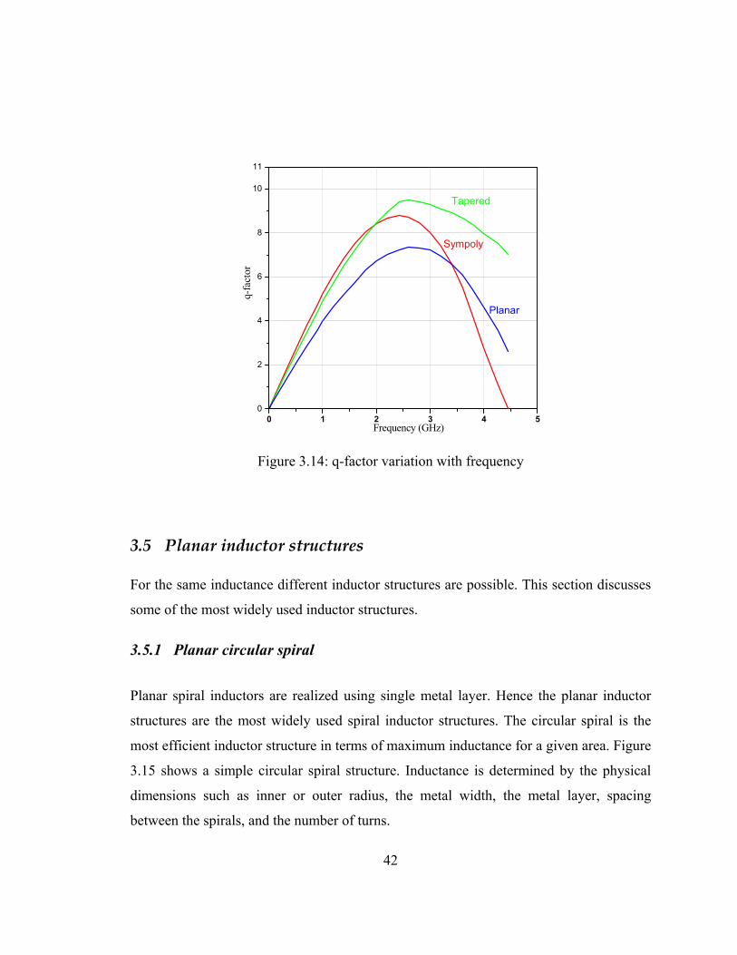
42
3.5 Planar inductor structures For the same inductance different inductor structures are possible. This section discusses
some of the most widely used inductor structures.
3.5.1 Planar circular spiral
Planar spiral inductors are realized using single metal layer. Hence the planar inductor
structures are the most widely used spiral inductor structures. The circular spiral is the
most efficient inductor structure in terms of maximum inductance for a given area. Figure
3.15 shows a simple circular spiral structure. Inductance is determined by the physical
dimensions such as inner or outer radius, the metal width, the metal layer, spacing
between the spirals, and the number of turns.
0 1 2 3 4 50
2
4
6
8
10
11
q-fa
ctor
Frequency (GHz)
Tapered
Sympoly
Planar
Figure 3.14: q-factor variation with frequency
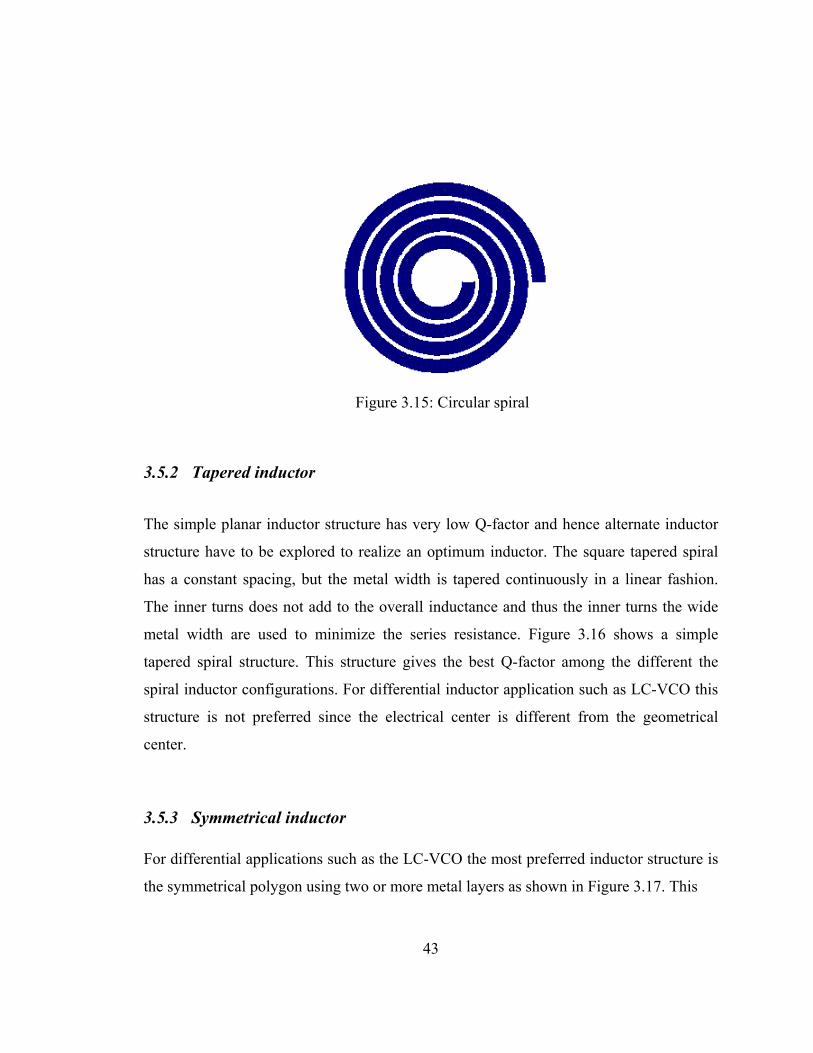
43
3.5.2 Tapered inductor
The simple planar inductor structure has very low Q-factor and hence alternate inductor
structure have to be explored to realize an optimum inductor. The square tapered spiral
has a constant spacing, but the metal width is tapered continuously in a linear fashion.
The inner turns does not add to the overall inductance and thus the inner turns the wide
metal width are used to minimize the series resistance. Figure 3.16 shows a simple
tapered spiral structure. This structure gives the best Q-factor among the different the
spiral inductor configurations. For differential inductor application such as LC-VCO this
structure is not preferred since the electrical center is different from the geometrical
center.
3.5.3 Symmetrical inductor For differential applications such as the LC-VCO the most preferred inductor structure is
the symmetrical polygon using two or more metal layers as shown in Figure 3.17. This
Figure 3.15: Circular spiral
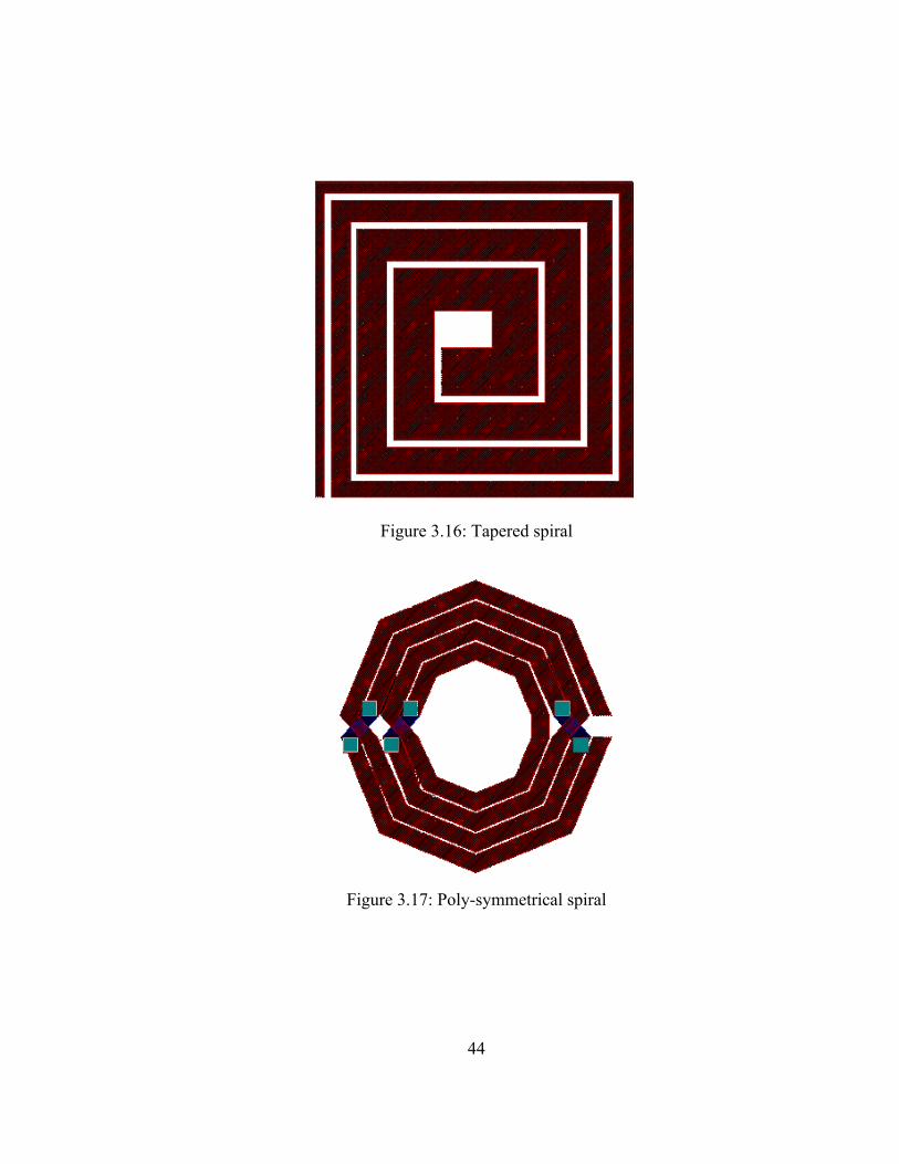
44
Figure 3.16: Tapered spiral
Figure 3.17: Poly-symmetrical spiral
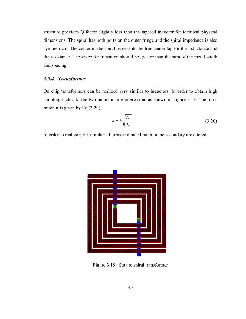
45
structure provides Q-factor slightly less than the tapered inductor for identical physical
dimensions. The spiral has both ports on the outer fringe and the spiral impedance is also
symmetrical. The center of the spiral represents the true center tap for the inductance and
the resistance. The space for transition should be greater than the sum of the metal width
and spacing.
3.5.4 Transformer On chip transformers can be realized very similar to inductors. In order to obtain high
coupling factor, k, the two inductors are interwound as shown in Figure 3.18. The turns
ration n is given by Eq (3.20)
1
2
LL
kn = (3.20)
In order to realize n ≠ 1 number of turns and metal pitch in the secondary are altered.
Figure 3.18 : Square spiral transformer
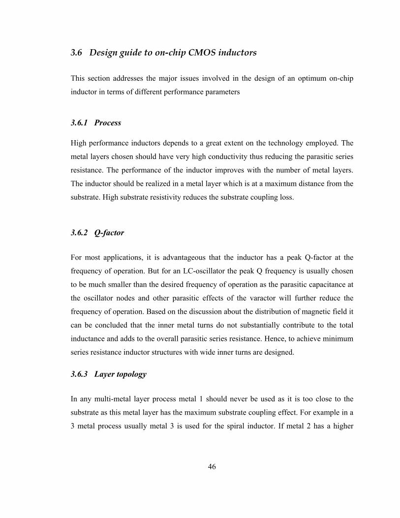
46
3.6 Design guide to on-chip CMOS inductors
This section addresses the major issues involved in the design of an optimum on-chip
inductor in terms of different performance parameters
3.6.1 Process High performance inductors depends to a great extent on the technology employed. The
metal layers chosen should have very high conductivity thus reducing the parasitic series
resistance. The performance of the inductor improves with the number of metal layers.
The inductor should be realized in a metal layer which is at a maximum distance from the
substrate. High substrate resistivity reduces the substrate coupling loss.
3.6.2 Q-factor
For most applications, it is advantageous that the inductor has a peak Q-factor at the
frequency of operation. But for an LC-oscillator the peak Q frequency is usually chosen
to be much smaller than the desired frequency of operation as the parasitic capacitance at
the oscillator nodes and other parasitic effects of the varactor will further reduce the
frequency of operation. Based on the discussion about the distribution of magnetic field it
can be concluded that the inner metal turns do not substantially contribute to the total
inductance and adds to the overall parasitic series resistance. Hence, to achieve minimum
series resistance inductor structures with wide inner turns are designed.
3.6.3 Layer topology
In any multi-metal layer process metal 1 should never be used as it is too close to the
substrate as this metal layer has the maximum substrate coupling effect. For example in a
3 metal process usually metal 3 is used for the spiral inductor. If metal 2 has a higher
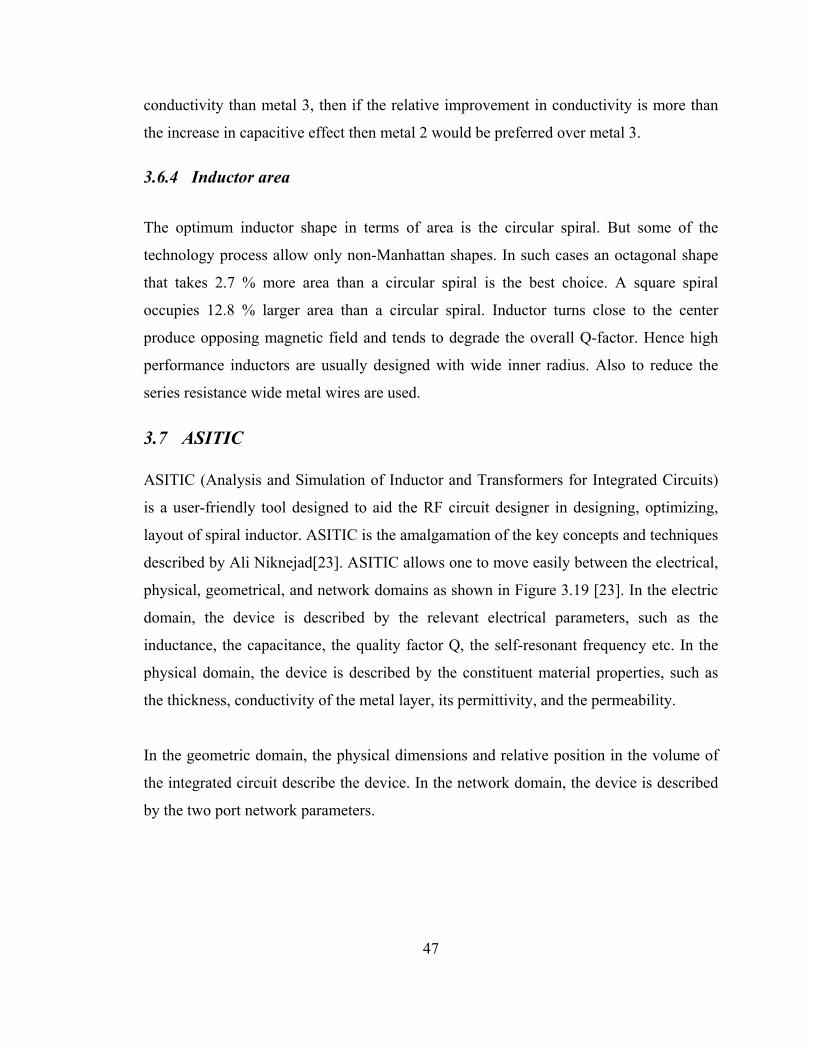
47
conductivity than metal 3, then if the relative improvement in conductivity is more than
the increase in capacitive effect then metal 2 would be preferred over metal 3.
3.6.4 Inductor area
The optimum inductor shape in terms of area is the circular spiral. But some of the
technology process allow only non-Manhattan shapes. In such cases an octagonal shape
that takes 2.7 % more area than a circular spiral is the best choice. A square spiral
occupies 12.8 % larger area than a circular spiral. Inductor turns close to the center
produce opposing magnetic field and tends to degrade the overall Q-factor. Hence high
performance inductors are usually designed with wide inner radius. Also to reduce the
series resistance wide metal wires are used.
3.7 ASITIC ASITIC (Analysis and Simulation of Inductor and Transformers for Integrated Circuits)
is a user-friendly tool designed to aid the RF circuit designer in designing, optimizing,
layout of spiral inductor. ASITIC is the amalgamation of the key concepts and techniques
described by Ali Niknejad[23]. ASITIC allows one to move easily between the electrical,
physical, geometrical, and network domains as shown in Figure 3.19 [23]. In the electric
domain, the device is described by the relevant electrical parameters, such as the
inductance, the capacitance, the quality factor Q, the self-resonant frequency etc. In the
physical domain, the device is described by the constituent material properties, such as
the thickness, conductivity of the metal layer, its permittivity, and the permeability.
In the geometric domain, the physical dimensions and relative position in the volume of
the integrated circuit describe the device. In the network domain, the device is described
by the two port network parameters.
48
Figure 3.19 : Different domains in ASITIC
49
The ability to move easily from one domain to the other is an important advantage of
ASITIC. This allows circuit designers and process engineers to optimize the device
structure and maximize the quality of passive devices. Other highly sophisticated
numerical tools such as Em solvers are comparatively slower than ASITIC by at least one
or two orders of magnitude slower since they employ complex mathematical operation.
ASITIC has also been designed to be a fairly flexible tool. As mentioned before, the
modern IC process allows highly complicated geometrical structures to be designed over
the Si substrate. The MEMS revolution is continuously expanding the possibilities as
more and more complex electromechanical structures are fabricated on Si. Thus one of
the major goals of ASITIC from the outset is to allow the analysis of an arbitrary
interconnection of metal structures over the Si substrates.
In summary, the goal of ASITIC has been to create an easy to use numerical software
package for the analysis and design of passive devices over the Si substrate. The key
criteria for the design of spiral inductors have been accuracy, flexibility, and efficiency.
Since 1995, ASITIC has been a freely available software package widely used in the IC
and EM community. To date over 1500 universities, organizations and commercial
entities have used ASITIC to solve practical and experimental problems. This has
resulted in great interaction between the users and creators of ASITIC, which has fueled
continuous evolution of ASITIC.
3.7.1 ASITIC organization Figure 3.20 [23] illustrates the block diagram of ASITIC modules. ASITIC is composed
of several software modules that interact over clearly defined interfaces. The user
interacts with ASITIC at the top level through the graphical and text interfaces The
technology file describes the pertinent process parameters such as the substrate layer
thickness, the conductivity, and the permittivity data, as well as the metal thickness. By
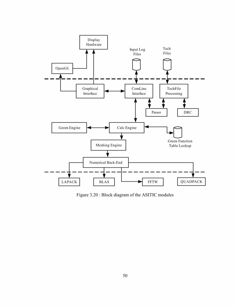
50
DisplayHardware
OpenGL
GraphicalInterface
ComLineInterface
TechFileProcessing
Geom Engine Calc Engine
Parser DRC
Meshing Engine
Numerical Back-End
LAPACK BLAS FFTW QUADPACK
Green FunctionTable Lookup
Input LogFiles
TechFiles
Figure 3.20 : Block diagram of the ASITIC modules
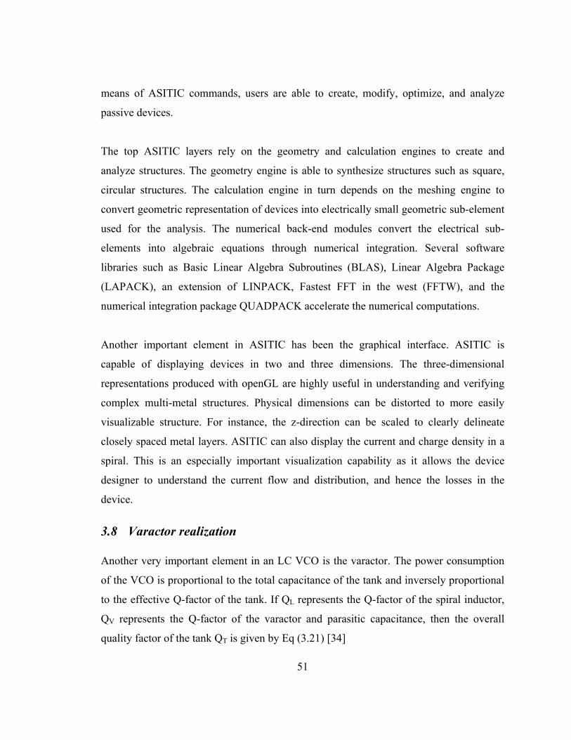
51
means of ASITIC commands, users are able to create, modify, optimize, and analyze
passive devices.
The top ASITIC layers rely on the geometry and calculation engines to create and
analyze structures. The geometry engine is able to synthesize structures such as square,
circular structures. The calculation engine in turn depends on the meshing engine to
convert geometric representation of devices into electrically small geometric sub-element
used for the analysis. The numerical back-end modules convert the electrical sub-
elements into algebraic equations through numerical integration. Several software
libraries such as Basic Linear Algebra Subroutines (BLAS), Linear Algebra Package
(LAPACK), an extension of LINPACK, Fastest FFT in the west (FFTW), and the
numerical integration package QUADPACK accelerate the numerical computations.
Another important element in ASITIC has been the graphical interface. ASITIC is
capable of displaying devices in two and three dimensions. The three-dimensional
representations produced with openGL are highly useful in understanding and verifying
complex multi-metal structures. Physical dimensions can be distorted to more easily
visualizable structure. For instance, the z-direction can be scaled to clearly delineate
closely spaced metal layers. ASITIC can also display the current and charge density in a
spiral. This is an especially important visualization capability as it allows the device
designer to understand the current flow and distribution, and hence the losses in the
device.
3.8 Varactor realization Another very important element in an LC VCO is the varactor. The power consumption
of the VCO is proportional to the total capacitance of the tank and inversely proportional
to the effective Q-factor of the tank. If QL represents the Q-factor of the spiral inductor,
QV represents the Q-factor of the varactor and parasitic capacitance, then the overall
quality factor of the tank QT is given by Eq (3.21) [34]
52
L
V
L
VL
VLT
QQQQQ
Q+
=+∗
=1
(3.21)
Usually QL varies from 6-10 depending on the process and the type of inductor structure.
Hence in order to obtain optimum QT one of the design challenges in a LC VCO is
achieving high Q-factor varactors in standard CMOS process. Another important design
parameter is the high tuning range represented by the maximum to minimum capacitance
ratio, min,max, / VV CC=ξ . The control voltage must be compatible with the supply voltage
and also provide linear capacitive variation. Hence one of the objectives of this research
work was to evaluate the different types of varactors in CMOS process in terms of tuning
range, Q-factor, optimum sizing, layout etc.
Two classes of device have been identified in CMOS process as varactors namely,
junction diodes and MOS capacitors. In each case the device should be placed in separate
wells in order to utilize the well potential as the control voltage. Hence there are losses
associated with the lightly doped well.
3.8.1 Varicap diodes Reverse biased diodes have been traditionally employed to realize a variable capacitor. In
an n-well process, diodes are implemented as p+/n-well. In differential VCO design these
diodes can be implemented in separate n-wells or for better symmetry a novel differential
structure in a common n-well can also be utilized. An simple electrical model for a
reverse biased diode consists of a variable capacitor, CV which can be expressed in terms
of control voltage Vcntl by Eq 3.22 [35]
MJSWcntl
eqMJ
cntl
eqV
PBSWV
PCJSW
PBV
ACJC
−
+
−
=
1
*
1
*
(3.22)
where Aeq , Peq are the diode area and perimeter respectively. The series equivalent
resistance rD is given by Eq (3.23)[35]
53
T
cntl
UNV
eqeq
TD e
PJSWAJSUNr *
***+
= (3.23)
In standard CMOS process the conductive substrate provides another parasitic resistance
Rsub through the lateral path from the junction to the small signal ground. The well
substrate capacitor CW trends to degrade the Q-factor of the tank for small unbalance in
the differential outputs. However this capacitance is negligible compared to CV as the
doping levels in the well and the substrate, are low and hence the depletion region is
wide. In order to avoid any further loss the control voltage node should be kept as a high
impedance node. Cext represents the additional capacitance due to the interconnections.
3.8.2 Conventional MOS varactor A conventional MOS varactor is formed by connecting the source, the drain and the body
to the control voltage while the gate connected to the tank. Here the capacitance value
depends on the voltage VBG between the body and the gate. For a PMOS capacitor, an
inversion channel with mobile holes builds up for VBG > |VT|, where |VT| is the threshold
voltage of the transistor. For VBG >> |VT|, the transistor operates in strong inversion and
for VBG << |VT|, the device enters accumulation region. The interface is high enough to
allow electrons to move freely. Thus in both strong inversion and accumulation regions,
the interface capacitance Cmos is equal to oxox tS /*ε , where S and tox are the channel area
and the oxide thickness, respectively. In between the extreme regions of operation there
exist intermediate region of operation where there are a few or very few mobile charge
carriers at the gate oxide interface. The effective capacitance can be expressed as Cox in
series with the parallel capacitance Cb and Ci, where Cb accounts for the hole modulation
in the weak and moderate depletion region and Ci accounts for the electron modulation in
the accumulation region. The region of operation is determined by whether Cb or Ci
dominates, if Cb >> Ci then the device is in moderate inversion and if Ci >> Cb the device
is in accumulation and if neither of them dominates the device is in weak inversion.
Figure 3.21 shows the capacitance variation with VBG.
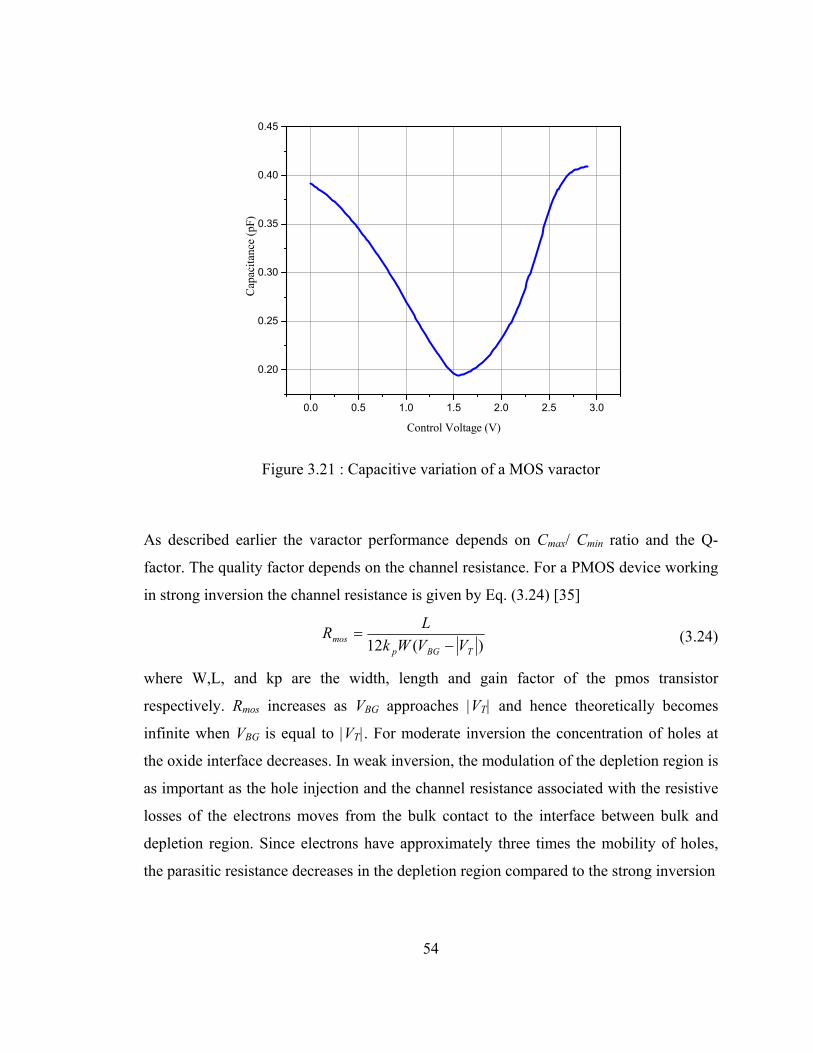
54
As described earlier the varactor performance depends on Cmax/ Cmin ratio and the Q-
factor. The quality factor depends on the channel resistance. For a PMOS device working
in strong inversion the channel resistance is given by Eq. (3.24) [35]
)(12 TBGpmos VVWk
LR−
= (3.24)
where W,L, and kp are the width, length and gain factor of the pmos transistor
respectively. Rmos increases as VBG approaches |VT| and hence theoretically becomes
infinite when VBG is equal to |VT|. For moderate inversion the concentration of holes at
the oxide interface decreases. In weak inversion, the modulation of the depletion region is
as important as the hole injection and the channel resistance associated with the resistive
losses of the electrons moves from the bulk contact to the interface between bulk and
depletion region. Since electrons have approximately three times the mobility of holes,
the parasitic resistance decreases in the depletion region compared to the strong inversion
0.0 0.5 1.0 1.5 2.0 2.5 3.0
0.20
0.25
0.30
0.35
0.40
0.45
Cap
acita
nce
(pF)
Control Voltage (V)
Figure 3.21 : Capacitive variation of a MOS varactor
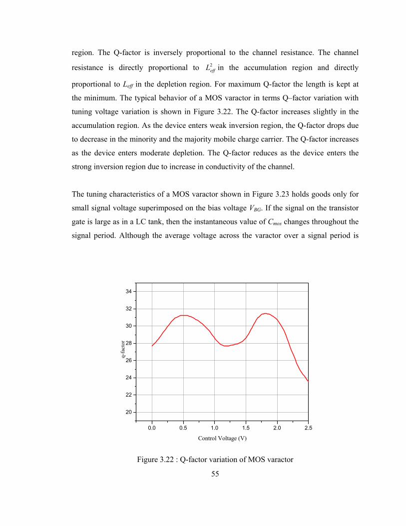
55
region. The Q-factor is inversely proportional to the channel resistance. The channel
resistance is directly proportional to 2effL in the accumulation region and directly
proportional to Leff in the depletion region. For maximum Q-factor the length is kept at
the minimum. The typical behavior of a MOS varactor in terms Q–factor variation with
tuning voltage variation is shown in Figure 3.22. The Q-factor increases slightly in the
accumulation region. As the device enters weak inversion region, the Q-factor drops due
to decrease in the minority and the majority mobile charge carrier. The Q-factor increases
as the device enters moderate depletion. The Q-factor reduces as the device enters the
strong inversion region due to increase in conductivity of the channel.
The tuning characteristics of a MOS varactor shown in Figure 3.23 holds goods only for
small signal voltage superimposed on the bias voltage VBG. If the signal on the transistor
gate is large as in a LC tank, then the instantaneous value of Cmos changes throughout the
signal period. Although the average voltage across the varactor over a signal period is
0.0 0.5 1.0 1.5 2.0 2.5
20
22
24
26
28
30
32
34
q-fa
ctor
Control Voltage (V)
Figure 3.22 : Q-factor variation of MOS varactor
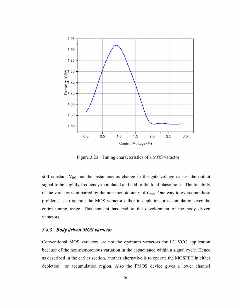
56
still constant VBG but the instantaneous change in the gate voltage causes the output
signal to be slightly frequency modulated and add to the total phase noise. The tunabilty
of the varactor is impaired by the non-monotonicity of Cmos. One way to overcome these
problems is to operate the MOS varactor either in depletion or accumulation over the
entire tuning range. This concept has lead to the development of the body driven
varactors.
3.8.3 Body driven MOS varactor Conventional MOS varactors are not the optimum varactors for LC VCO application
because of the non-monotonous variation in the capacitance within a signal cycle. Hence
as described in the earlier section, another alternative is to operate the MOSFET in either
depletion or accumulation region. Also the PMOS device gives a lower channel
0.0 0.5 1.0 1.5 2.0 2.5 3.0
1.55
1.60
1.65
1.70
1.75
1.80
1.85
1.90
1.95
Freq
uenc
y (G
Hz)
Control Voltage (V)
Figure 3.23 : Tuning characteristics of a MOS varactor
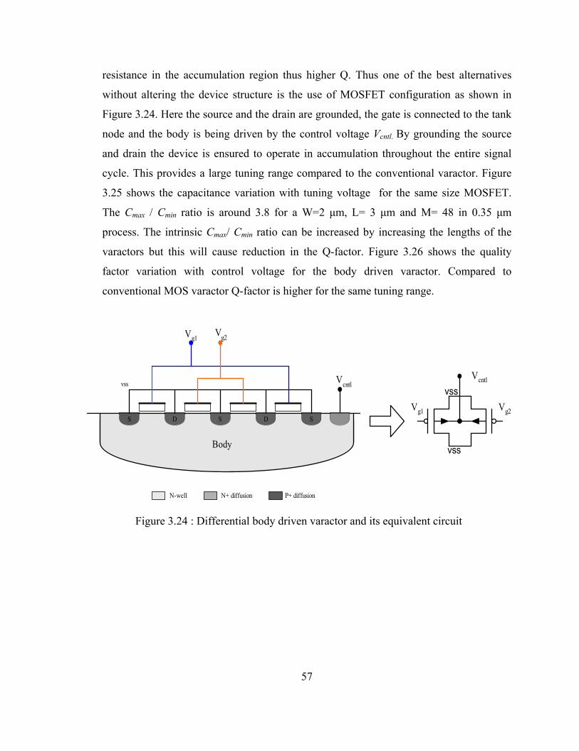
57
resistance in the accumulation region thus higher Q. Thus one of the best alternatives
without altering the device structure is the use of MOSFET configuration as shown in
Figure 3.24. Here the source and the drain are grounded, the gate is connected to the tank
node and the body is being driven by the control voltage Vcntl. By grounding the source
and drain the device is ensured to operate in accumulation throughout the entire signal
cycle. This provides a large tuning range compared to the conventional varactor. Figure
3.25 shows the capacitance variation with tuning voltage for the same size MOSFET.
The Cmax / Cmin ratio is around 3.8 for a W=2 µm, L= 3 µm and M= 48 in 0.35 µm
process. The intrinsic Cmax/ Cmin ratio can be increased by increasing the lengths of the
varactors but this will cause reduction in the Q-factor. Figure 3.26 shows the quality
factor variation with control voltage for the body driven varactor. Compared to
conventional MOS varactor Q-factor is higher for the same tuning range.
Vg1 Vg2
vss
S SD D S
Body
Vcntl
N-well N+ diffusion P+ diffusion
Vcntl
vss
vss
Vg1 Vg2
Figure 3.24 : Differential body driven varactor and its equivalent circuit
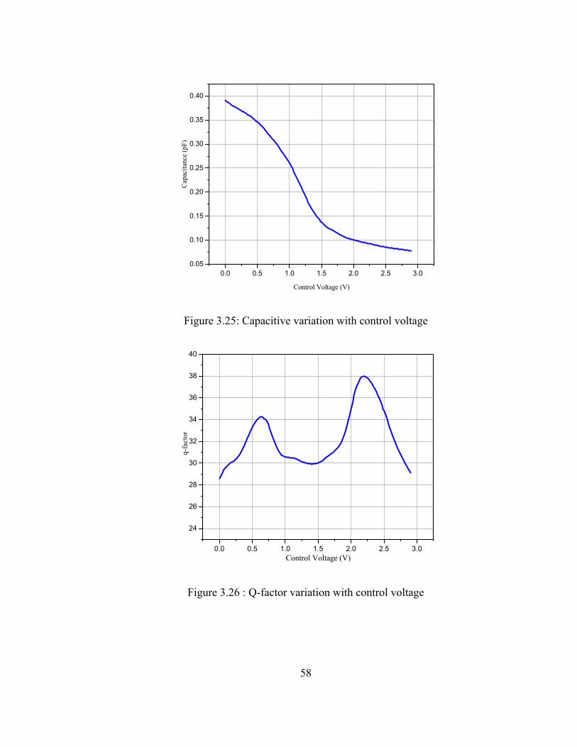
58
0.0 0.5 1.0 1.5 2.0 2.5 3.00.05
0.10
0.15
0.20
0.25
0.30
0.35
0.40
Cap
acita
nce
(pF)
Control Voltage (V)
Figure 3.25: Capacitive variation with control voltage
0.0 0.5 1.0 1.5 2.0 2.5 3.0
24
26
28
30
32
34
36
38
40
q-fa
ctor
Control Voltage (V)
Figure 3.26 : Q-factor variation with control voltage
59
3.9 Body driven MOS varactor modeling This section describes the general behavior model for body driven varactors. The main
capacitor of concern is the gate to body capacitance, but there exist additional parasitic
capacitance associated with the source and drain. Further, the MOS varactor as discussed
in the previous is not an ideal capacitor and thus has its associated parasitic substrate and
channel resistance. For a better understanding the MOS transistor can be viewed as
consisting of two parts. The part between the source and the drain containing the
inversion layer and the depletion region as well as the region between the oxide and the
gate above them will be described as the intrinsic part. The part surrounded by the source
and the drain resistance, the junction capacitance from the source, the drain and the gate
to the body, the resistance of the body constitutes the extrinsic part. The effective
capacitance between any terminals can thus be expressed as the parallel combination of
the intrinsic and the extrinsic effects.
The parasitic extrinsic overlap capacitance between the gate and the source and the gate
and the drain expressed as Cgse and Cgde respectively can be roughly estimated as
WLDCCC oxgdegse **'== (3.25)
where Cox′ is the oxide capacitance per unit area which is inversely proportional to the
oxide thickness, LD is the overlap length and W is the width of the device. In addition to
this another prominent extrinsic capacitance is the gate-body capacitance expressed as
effeffoxgbe LWCC **'= (3.26)
where Cox′ is the oxide capacitance per unit area, Weff and Leff are the effective width and
length of the device respectively. In addition to the overlap capacitance there exist two
junction capacitances Cbse between the body and the source and Cbde between the body
and the drain. Each of these consists of a bottom wall part and a sidewall part. These
capacitance can be expressed by Eq. (3.24) [36]
( )[ ] [ ] 21 )/(1/1 2
*
1
'
ηη φφ SB
joS
SB
jobse V
CPVAsC
C+
++
= (3.27)
60
( )[ ] [ ] 21 )/(1/1 2
*
1
'
ηη φφ DB
joD
DB
joDbde V
CP
V
CAC
++
+= (3.28)
where Cjo’ is the bottom wall junction zero-bias capacitance per unit area, Cjo* is the
sidewall junction zero-bias capacitance per unit area, AS and AD represents the source
and the drain bottom wall junction area, PS and PD represents the source and drain
sidewall perimeter, φ1 is the bottom wall junction built in potential, η1 is the bottom wall
junction characteristic exponent, φ2 is the sidewall junction built in potential, η2 is the
sidewall junction characteristic exponent. The characteristic constants in the above
equations can be calculated from the shapes and doping profiles of the junction.
Intrinsic capacitances are due to the charges inside the intrinsic part. These charges and
the resulting capacitance depends on the region of operation. In the current design the
body driven varactor is forced to operate in the accumulation region. In the accumulation
mode the gate to body capacitance Cgbi, given by Eq (3.29) [37] is the only prominent
capacitance for a PMOS transistor. All other capacitance can be neglected.
[ ]21
15
1)/exp(
1)/exp(10785.1
−+−
−×= +−
kTqkTq
kTqNC
ss
sdgbi
ψψ
ψ (3.29)
where Nd+ represents the doping concentration of the n-well, ψs is the potential obtained
from the Poisson’s equation considering the contribution of electrons and holes at the
Si/SiO2 interface expressed in terms of gate voltage VGB by Eq. (3.30)
sss
ox
oxdFBGB kTq
kTqt
NVV ψψψ
ε+
−−+××+= +−
2117 1)exp(10282.9 (3.30)
The final simplified body driven varactor’s behavioral model is shown in Figure 3.27. RG
represents the gate resistance, RSB or RDB represents the reverse biased diode resistance
between the body and the drain which is usually very high, RGB is the vertical resistance
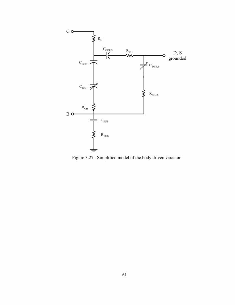
61
CSUB
RG
CGDE,S RCH
CGBE
CGBI
RGB
CDBE,S
RSB,DB
G
D, Sgrounded
B
RSUB
Figure 3.27 : Simplified model of the body driven varactor
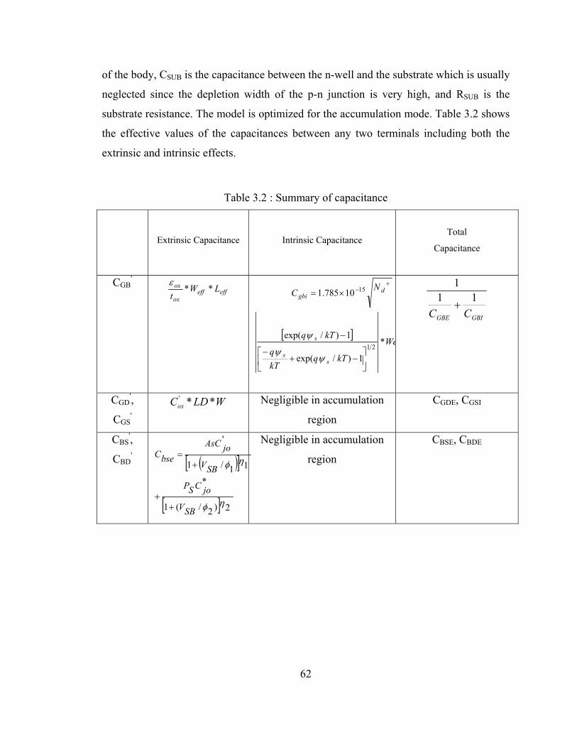
62
of the body, CSUB is the capacitance between the n-well and the substrate which is usually
neglected since the depletion width of the p-n junction is very high, and RSUB is the
substrate resistance. The model is optimized for the accumulation mode. Table 3.2 shows
the effective values of the capacitances between any two terminals including both the
extrinsic and intrinsic effects.
Table 3.2 : Summary of capacitance
Extrinsic Capacitance Intrinsic Capacitance
Total
Capacitance
CGB'
effeffox
ox LWt
**ε
[ ]We
kTqkTq
kTq
NC
ss
s
dgbi
*
1)/exp(
1)/exp(
10785.1
21
15
−+
−
−
×=+
−
ψψ
ψ
GBIGBE CC11
1
+
CGD',
CGS'
WLDCox **' Negligible in accumulation
region
CGDE, CGSI
CBS',
CBD' ( )[ ]
[ ] 2)2/(1
*
11/1
'
ηφ
ηφ
SBV
joCSP
SBV
joAsCbseC
++
+=
Negligible in accumulation
region
CBSE, CBDE
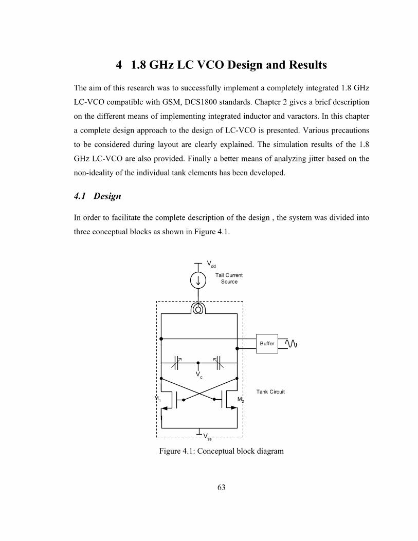
63
4 1.8 GHz LC VCO Design and Results The aim of this research was to successfully implement a completely integrated 1.8 GHz
LC-VCO compatible with GSM, DCS1800 standards. Chapter 2 gives a brief description
on the different means of implementing integrated inductor and varactors. In this chapter
a complete design approach to the design of LC-VCO is presented. Various precautions
to be considered during layout are clearly explained. The simulation results of the 1.8
GHz LC-VCO are also provided. Finally a better means of analyzing jitter based on the
non-ideality of the individual tank elements has been developed.
4.1 Design In order to facilitate the complete description of the design , the system was divided into
three conceptual blocks as shown in Figure 4.1.
M1 M2
Vc
Vss
Vdd
Buffer
Tail CurrentSource
Tank Circuit
Figure 4.1: Conceptual block diagram
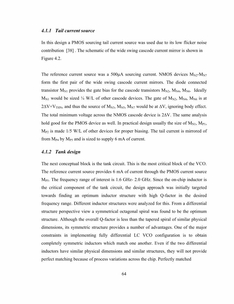
64
4.1.1 Tail current source In this design a PMOS sourcing tail current source was used due to its low flicker noise
contribution [38] . The schematic of the wide swing cascode current mirror is shown in
Figure 4.2.
The reference current source was a 500µA sourcing current. NMOS devices MN2-MN7
form the first pair of the wide swing cascode current mirrors. The diode connected
transistor MN1 provides the gate bias for the cascode transistors MN2, MN4, MN6. Ideally
MN1 would be sized ¼ W/L of other cascode devices. The gate of MN2, MN4, MN6 is at
2∆V+VTHN, and thus the source of MN3, MN5, MN7 would be at ∆V, ignoring body effect.
The total minimum voltage across the NMOS cascode device is 2∆V. The same analysis
hold good for the PMOS device as well. In practical design usually the size of MN1, MP1,
MP2 is made 1/5 W/L of other devices for proper biasing. The tail current is mirrored of
from MP4 by MP5 and is sized to supply 6 mA of current.
4.1.2 Tank design The next conceptual block is the tank circuit. This is the most critical block of the VCO.
The reference current source provides 6 mA of current through the PMOS current source
MP5. The frequency range of interest is 1.6 GHz- 2.0 GHz. Since the on-chip inductor is
the critical component of the tank circuit, the design approach was initially targeted
towards finding an optimum inductor structure with high Q-factor in the desired
frequency range. Different inductor structures were analyzed for this. From a differential
structure perspective view a symmetrical octagonal spiral was found to be the optimum
structure. Although the overall Q-factor is less than the tapered spiral of similar physical
dimensions, its symmetric structure provides a number of advantages. One of the major
constraints in implementing fully differential LC VCO configuration is to obtain
completely symmetric inductors which match one another. Even if the two differential
inductors have similar physical dimensions and similar structures, they will not provide
perfect matching because of process variations across the chip. Perfectly matched
65
MP110/0.7
MN14.4/0.7
MP5600/0.7
MP450/0.7
MP350/0.7
MP210/0.7
MN222/0.7
MN322/0.7
MN422/0.7
MN522/0.7
MN722/0.7
MN622/0.7
IB500u
VDD
VSS
IT
Figure 4.2: Current source schematic
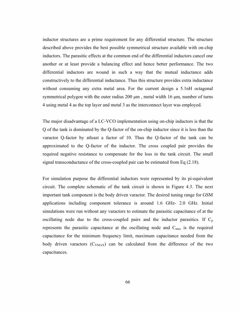
66
inductor structures are a prime requirement for any differential structure. The structure
described above provides the best possible symmetrical structure available with on-chip
inductors. The parasitic effects at the common end of the differential inductors cancel one
another or at least provide a balancing effect and hence better performance. The two
differential inductors are wound in such a way that the mutual inductance adds
constructively to the differential inductance. Thus this structure provides extra inductance
without consuming any extra metal area. For the current design a 5.1nH octagonal
symmetrical polygon with the outer radius 200 µm , metal width 16 µm, number of turns
4 using metal 4 as the top layer and metal 3 as the interconnect layer was employed.
The major disadvantage of a LC-VCO implementation using on-chip inductors is that the
Q of the tank is dominated by the Q-factor of the on-chip inductor since it is less than the
varactor Q-factor by atleast a factor of 10. Thus the Q-factor of the tank can be
approximated to the Q-factor of the inductor. The cross coupled pair provides the
required negative resistance to compensate for the loss in the tank circuit. The small
signal transconductance of the cross-coupled pair can be estimated from Eq (2.18).
For simulation purpose the differential inductors were represented by its pi-equivalent
circuit. The complete schematic of the tank circuit is shown in Figure 4.3. The next
important tank component is the body driven varactor. The desired tuning range for GSM
applications including component tolerance is around 1.6 GHz- 2.0 GHz. Initial
simulations were run without any varactors to estimate the parasitic capacitance of at the
oscillating node due to the cross-coupled pairs and the inductor parasitics. If Cp
represents the parasitic capacitance at the oscillating node and Cmax is the required
capacitance for the minimum frequency limit, maximum capacitance needed from the
body driven varactors (CVMAX) can be calculated from the difference of the two
capacitances.
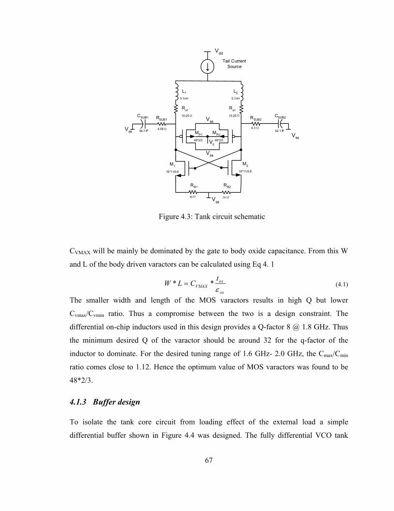
67
CVMAX will be mainly be dominated by the gate to body oxide capacitance. From this W
and L of the body driven varactors can be calculated using Eq 4. 1
ox
oxVMAX
tCLW
ε** = (4.1)
The smaller width and length of the MOS varactors results in high Q but lower
Cvmax/Cvmin ratio. Thus a compromise between the two is a design constraint. The
differential on-chip inductors used in this design provides a Q-factor 8 @ 1.8 GHz. Thus
the minimum desired Q of the varactor should be around 32 for the q-factor of the
inductor to dominate. For the desired tuning range of 1.6 GHz- 2.0 GHz, the Cmax/Cmin
ratio comes close to 1.12. Hence the optimum value of MOS varactors was found to be
48*2/3.
4.1.3 Buffer design To isolate the tank core circuit from loading effect of the external load a simple
differential buffer shown in Figure 4.4 was designed. The fully differential VCO tank
VssVss
M1
16*11/0.8
M2
16*11/0.8
Vc
Vss
Vdd
Tail CurrentSource
RB1 RB2
Vss
Vss
50 Ω 50 Ω
MP1 MP2
48*2/3 48*2/3
L1
5.1nH
L2
5.1nH
Rs1
10.25 Ω
Rs1
10.25 ΩRSUB1CSUB1
4.58 Ω56.7 fF
RSUB2
4.3 Ω
CSUB2
52.1 fF
Figure 4.3: Tank circuit schematic
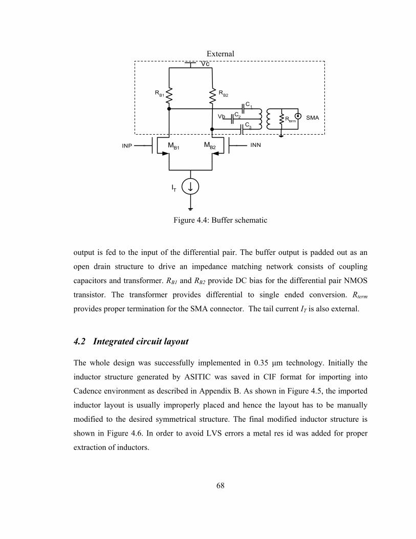
68
output is fed to the input of the differential pair. The buffer output is padded out as an
open drain structure to drive an impedance matching network consists of coupling
capacitors and transformer. RB1 and RB2 provide DC bias for the differential pair NMOS
transistor. The transformer provides differential to single ended conversion. Rterm
provides proper termination for the SMA connector. The tail current IT is also external.
4.2 Integrated circuit layout The whole design was successfully implemented in 0.35 µm technology. Initially the
inductor structure generated by ASITIC was saved in CIF format for importing into
Cadence environment as described in Appendix B. As shown in Figure 4.5, the imported
inductor layout is usually improperly placed and hence the layout has to be manually
modified to the desired symmetrical structure. The final modified inductor structure is
shown in Figure 4.6. In order to avoid LVS errors a metal res id was added for proper
extraction of inductors.
External
INP INN
Vc
RB1 RB2
IT
C1
C2
C3
RtermSMA
MB1 MB2
Vb
Figure 4.4: Buffer schematic
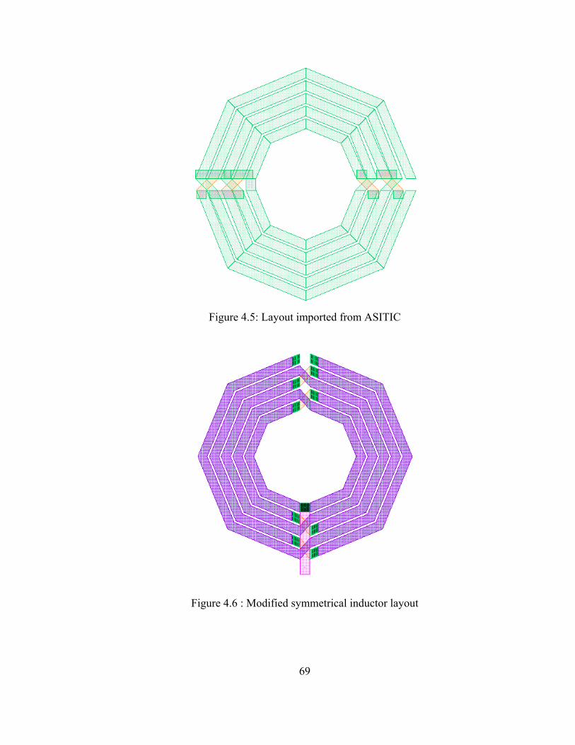
69
Figure 4.5: Layout imported from ASITIC
Figure 4.6 : Modified symmetrical inductor layout
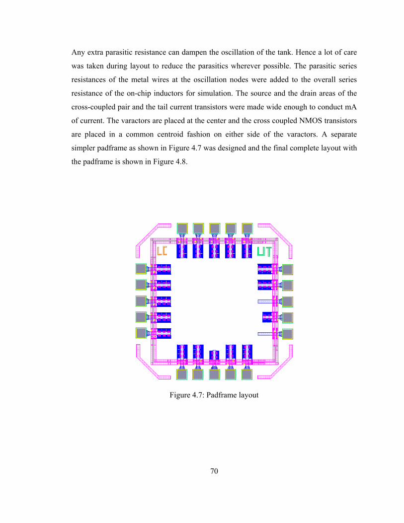
70
Any extra parasitic resistance can dampen the oscillation of the tank. Hence a lot of care
was taken during layout to reduce the parasitics wherever possible. The parasitic series
resistances of the metal wires at the oscillation nodes were added to the overall series
resistance of the on-chip inductors for simulation. The source and the drain areas of the
cross-coupled pair and the tail current transistors were made wide enough to conduct mA
of current. The varactors are placed at the center and the cross coupled NMOS transistors
are placed in a common centroid fashion on either side of the varactors. A separate
simpler padframe as shown in Figure 4.7 was designed and the final complete layout with
the padframe is shown in Figure 4.8.
Figure 4.7: Padframe layout
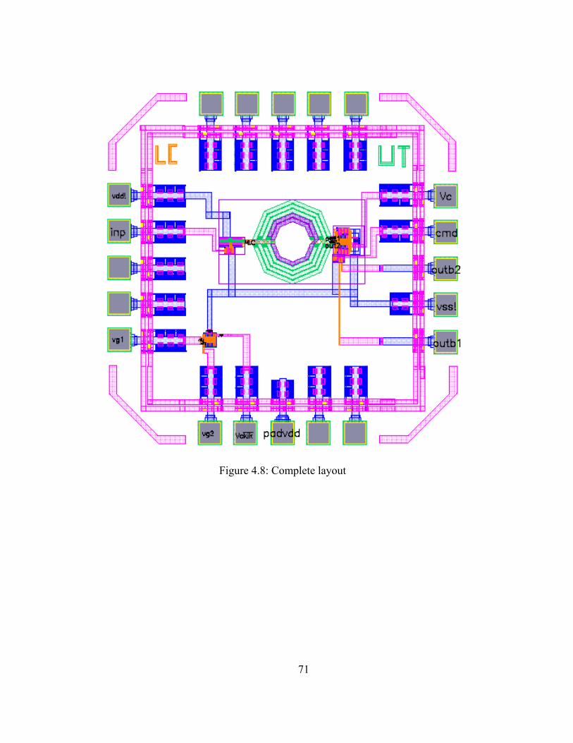
71
Figure 4.8: Complete layout
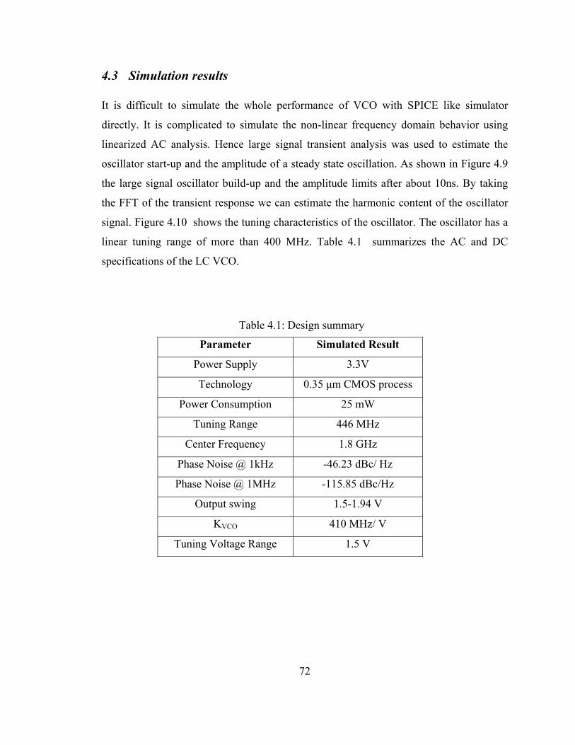
72
4.3 Simulation results It is difficult to simulate the whole performance of VCO with SPICE like simulator
directly. It is complicated to simulate the non-linear frequency domain behavior using
linearized AC analysis. Hence large signal transient analysis was used to estimate the
oscillator start-up and the amplitude of a steady state oscillation. As shown in Figure 4.9
the large signal oscillator build-up and the amplitude limits after about 10ns. By taking
the FFT of the transient response we can estimate the harmonic content of the oscillator
signal. Figure 4.10 shows the tuning characteristics of the oscillator. The oscillator has a
linear tuning range of more than 400 MHz. Table 4.1 summarizes the AC and DC
specifications of the LC VCO.
Table 4.1: Design summary
Parameter Simulated Result
Power Supply 3.3V
Technology 0.35 µm CMOS process
Power Consumption 25 mW
Tuning Range 446 MHz
Center Frequency 1.8 GHz
Phase Noise @ 1kHz -46.23 dBc/ Hz
Phase Noise @ 1MHz -115.85 dBc/Hz
Output swing 1.5-1.94 V
KVCO 410 MHz/ V
Tuning Voltage Range 1.5 V
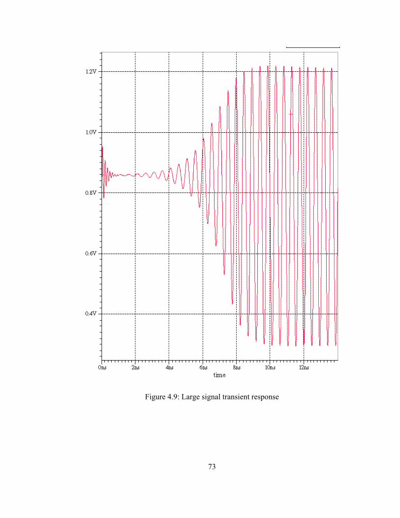
73
Figure 4.9: Large signal transient response
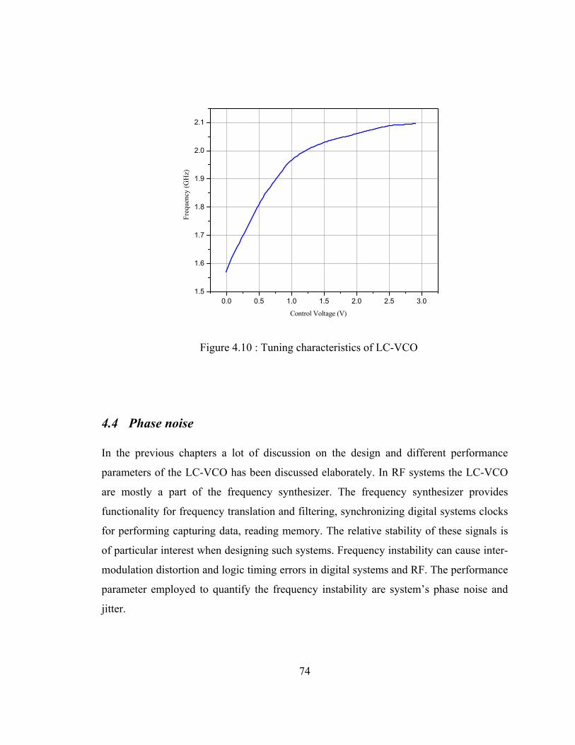
74
4.4 Phase noise In the previous chapters a lot of discussion on the design and different performance
parameters of the LC-VCO has been discussed elaborately. In RF systems the LC-VCO
are mostly a part of the frequency synthesizer. The frequency synthesizer provides
functionality for frequency translation and filtering, synchronizing digital systems clocks
for performing capturing data, reading memory. The relative stability of these signals is
of particular interest when designing such systems. Frequency instability can cause inter-
modulation distortion and logic timing errors in digital systems and RF. The performance
parameter employed to quantify the frequency instability are system’s phase noise and
jitter.
0.0 0.5 1.0 1.5 2.0 2.5 3.01.5
1.6
1.7
1.8
1.9
2.0
2.1
Freq
uenc
y (G
Hz)
Control Voltage (V)
Figure 4.10 : Tuning characteristics of LC-VCO
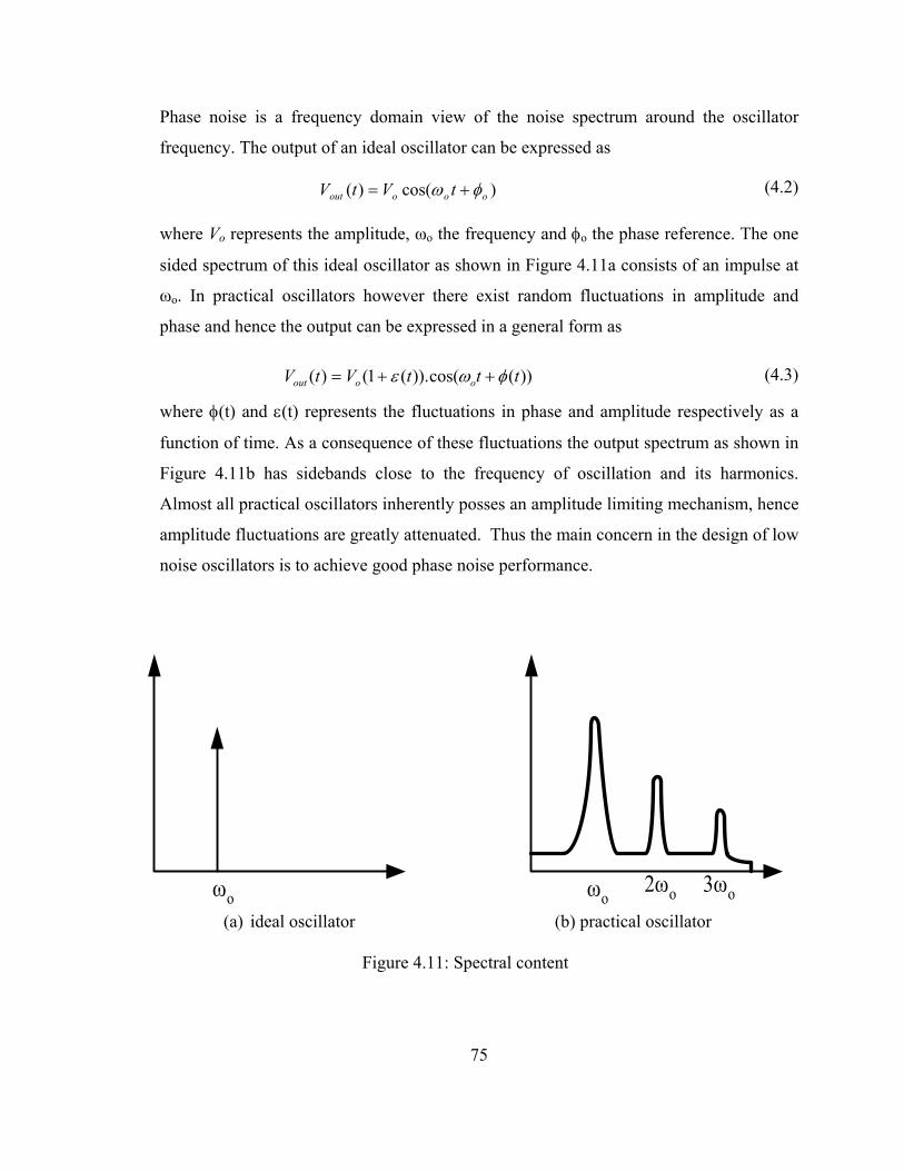
75
Phase noise is a frequency domain view of the noise spectrum around the oscillator
frequency. The output of an ideal oscillator can be expressed as
)cos()( oooout tVtV φω += (4.2)
where Vo represents the amplitude, ωo the frequency and φo the phase reference. The one
sided spectrum of this ideal oscillator as shown in Figure 4.11a consists of an impulse at
ωo. In practical oscillators however there exist random fluctuations in amplitude and
phase and hence the output can be expressed in a general form as
))(cos()).(1()( tttVtV ooout φωε ++= (4.3)
where φ(t) and ε(t) represents the fluctuations in phase and amplitude respectively as a
function of time. As a consequence of these fluctuations the output spectrum as shown in
Figure 4.11b has sidebands close to the frequency of oscillation and its harmonics.
Almost all practical oscillators inherently posses an amplitude limiting mechanism, hence
amplitude fluctuations are greatly attenuated. Thus the main concern in the design of low
noise oscillators is to achieve good phase noise performance.
ωo2ωo 3ωoωo
(a) ideal oscillator (b) practical oscillator
Figure 4.11: Spectral content
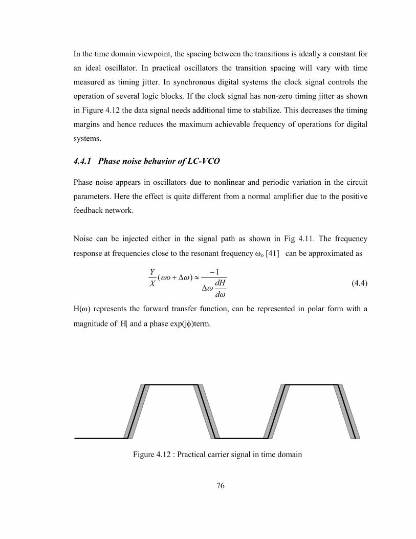
76
In the time domain viewpoint, the spacing between the transitions is ideally a constant for
an ideal oscillator. In practical oscillators the transition spacing will vary with time
measured as timing jitter. In synchronous digital systems the clock signal controls the
operation of several logic blocks. If the clock signal has non-zero timing jitter as shown
in Figure 4.12 the data signal needs additional time to stabilize. This decreases the timing
margins and hence reduces the maximum achievable frequency of operations for digital
systems.
4.4.1 Phase noise behavior of LC-VCO Phase noise appears in oscillators due to nonlinear and periodic variation in the circuit
parameters. Here the effect is quite different from a normal amplifier due to the positive
feedback network.
Noise can be injected either in the signal path as shown in Fig 4.11. The frequency
response at frequencies close to the resonant frequency ωo [41] can be approximated as
ωω
ωω
ddH
oXY
∆
−≈∆+
1)( (4.4)
H(ω) represents the forward transfer function, can be represented in polar form with a
magnitude of |H| and a phase exp(jφ)term.
Figure 4.12 : Practical carrier signal in time domain
77
2222
Hdd
dHd
ddH
ωφ
ωω+= (4.5)
For a LC-VCO the H(ω) magnitude does not vary a lot with frequency for small offsets
from the resonant frequency and hence the magnitude term in Eq (4.5) can be ignored.
Also |H| is close to unity for steady state oscillations. Eq (4.5) can now be rewritten as
22
2
)(
1)(
ωφω
ω
dd
jXY
∆
= (4.6)
From the definition of the Q-factor, Eq (2.18) in Chapter 2 can be expressed in terms of
Q-factor as
2
2
2
41)(
∆=
ωωω o
Qj
XY
(4.7)
Eq (4.7) is commonly known as “Lessons’s equation [42] represents both the amplitude
and phase noise effects. The noise performance of an LC oscillator depends extensively
on the Q-factor of the tank, hence a lot of effort is expended on the design of high Q-
factor on-chip inductors. Non-linear behavior of the oscillator system introduces noise
folding and thus need additional terms in Eq (4.7) to represent the non-linear behavior.
Similar analysis can be performed for noise source injected through the control path. Any
noise signal in the control voltage also affects the frequency of the oscillation and thus
the phase noise as a frequency modulated signal.
The above discussion was based on the general influence of noise on the phase noise of
the system. From the designer’s perspective, a better means of analyzing phase noise is to
study the influence of various circuit components on the total phase noise. In this current
research the influence of individual components noise on the total oscillator phase noise
has been analyzed elaborately.
78
A variation in the tail current source IT introduces noise in the signal path as well as in
the control path. The output common mode level (VCM) of the cross-coupled pair can be
approximated as
c
TTHNCM gm
IVV += (4.8)
To examine the variation of tail current source on the phase noise assume a small
sinusoidal current source )cos( tI mT ω∆ superimposed on the tail current IT produces an
additional variation ∆VBG across the varactor and hence the output frequency varies from
its ideal value. Eq (4.9) [40] quantifies the frequency fluctuation induced by the tail
current variation
∂
∂
∂∂
=
∂∂
T
BG
BG
o
T
o
IV
VIωω
(4.9)
The first term in Eq (4.9) is the VCO gain KVCO and the second term can be
approximated from Eq (4.8) as )2/(1 nmosgm . Hence high transconductance of the cross-
coupled pair gives better phase noise performance. The effect of varactor voltage
fluctuation on phase noise is similar to the frequency modulation effect produced by the
tail current source. Variation in the tail current source also affects the amplitude of the
output, thus indirectly induces a frequency fluctuations adding to the total phase noise.
Sensitivity of frequency fluctuation with amplitude variation KAo is more complex due to
the non-linear behavior of the tank and also sensitivity changes its sign. Usually the
relation is derived numerically for given values of varactor bias voltage and amplitude.
Another source of upconverted phase noise is the power supply noise. In this design
PMOS transistors have been employed as tail current source due to their low flicker noise
contribution compared to NMOS transistors. A cascode tail current can provide a better
power supply noise rejection; however this reduces the effective swing of the tank and
hence is not an effective solution for low voltage designs. The phase noise is also affected
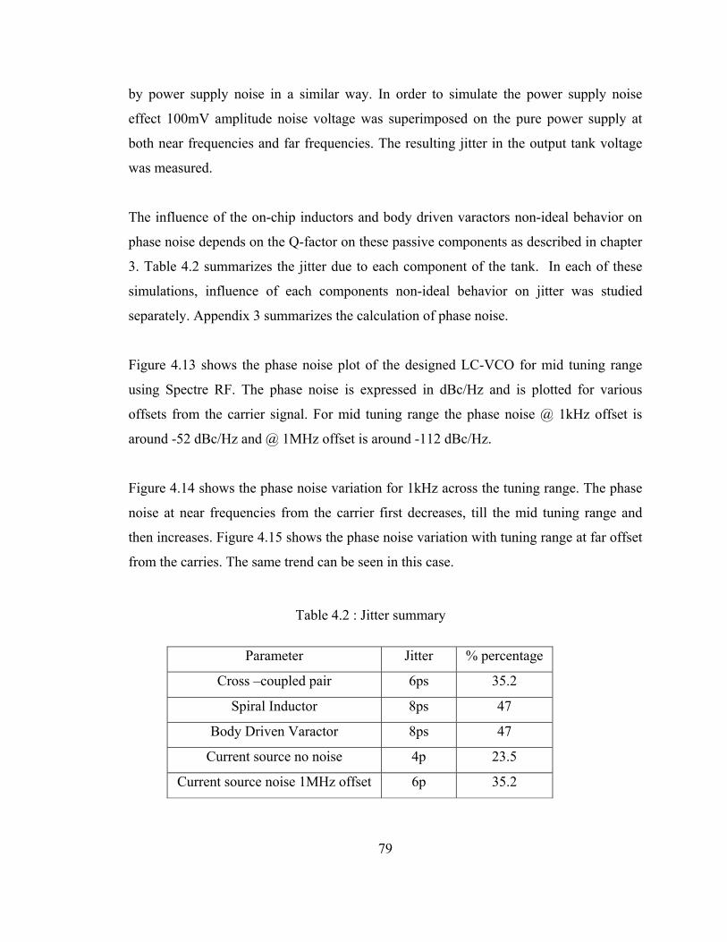
79
by power supply noise in a similar way. In order to simulate the power supply noise
effect 100mV amplitude noise voltage was superimposed on the pure power supply at
both near frequencies and far frequencies. The resulting jitter in the output tank voltage
was measured.
The influence of the on-chip inductors and body driven varactors non-ideal behavior on
phase noise depends on the Q-factor on these passive components as described in chapter
3. Table 4.2 summarizes the jitter due to each component of the tank. In each of these
simulations, influence of each components non-ideal behavior on jitter was studied
separately. Appendix 3 summarizes the calculation of phase noise.
Figure 4.13 shows the phase noise plot of the designed LC-VCO for mid tuning range
using Spectre RF. The phase noise is expressed in dBc/Hz and is plotted for various
offsets from the carrier signal. For mid tuning range the phase noise @ 1kHz offset is
around -52 dBc/Hz and @ 1MHz offset is around -112 dBc/Hz.
Figure 4.14 shows the phase noise variation for 1kHz across the tuning range. The phase
noise at near frequencies from the carrier first decreases, till the mid tuning range and
then increases. Figure 4.15 shows the phase noise variation with tuning range at far offset
from the carries. The same trend can be seen in this case.
Table 4.2 : Jitter summary
Parameter Jitter % percentage
Cross –coupled pair 6ps 35.2
Spiral Inductor 8ps 47
Body Driven Varactor 8ps 47
Current source no noise 4p 23.5
Current source noise 1MHz offset 6p 35.2
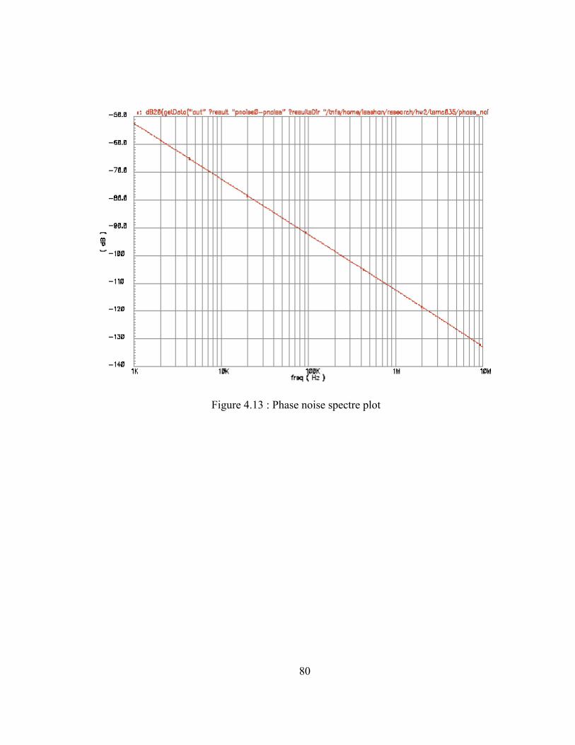
80
Figure 4.13 : Phase noise spectre plot
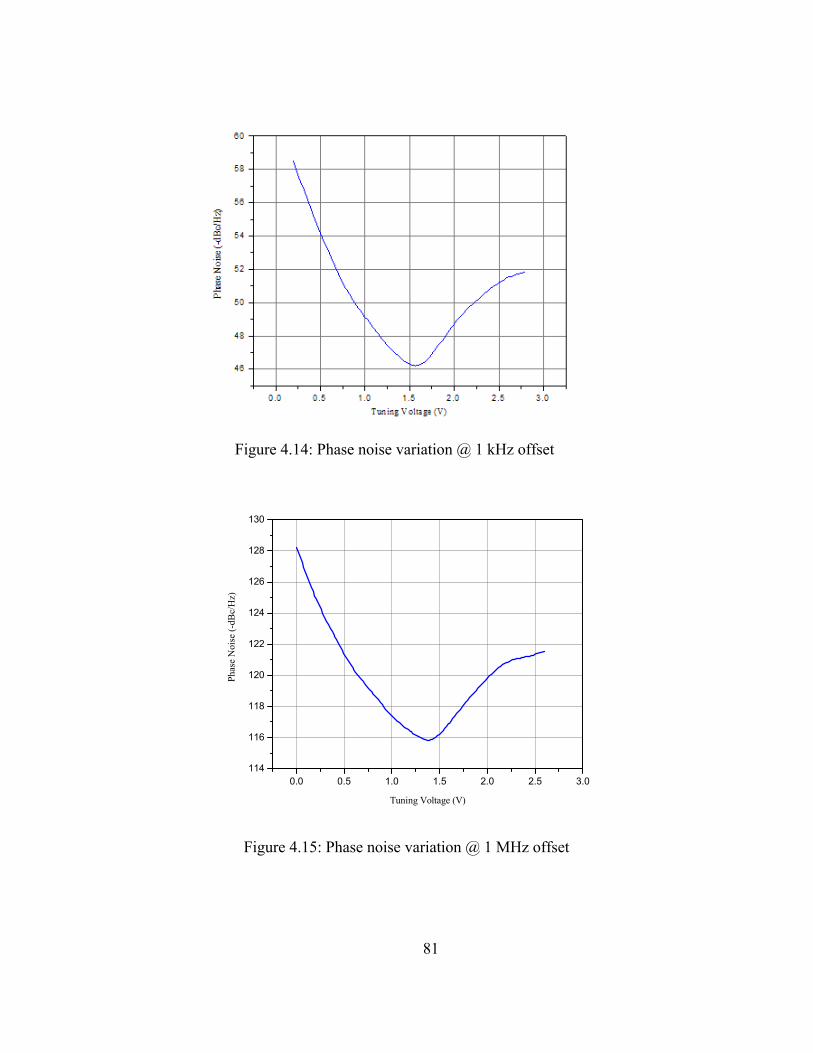
81
Figure 4.14: Phase noise variation @ 1 kHz offset
0.0 0.5 1.0 1.5 2.0 2.5 3.0114
116
118
120
122
124
126
128
130
Phas
e N
oise
(-dB
c/H
z)
Tuning Voltage (V)
Figure 4.15: Phase noise variation @ 1 MHz offset

82
5 CONCLUSION AND FUTURE WORK
5.1 Conclusion A complete integrated LC-VCO compatible with the GSM 1800, DCS receiver has been
designed in standard CMOS 0.35 µm technology. The design specifications were all met
with sufficient margin. The designed integrated LC-VCO has a linear tuning range from
1.595 GHz – 2.05 GHz. The designed VCO has a gain of 410 MHz/V. The worst case
phase noise in dBc/Hz at 1 kHz offset across the tuning range is -46.23 dBc/Hz and @ 1
MHz offset from the carrier is -115.85 dBc/Hz. The power consumption of the block,
excluding the output buffer power consumption is approximately 8.78 mW. Currently the
design has been sent for fabrication and test board is being designed.
5.2 Future work
The major shortcoming of the spiral inductor is the poor Q-factor compared with inductor
implementation. Hence one of the future goals is to explore different means of improving
the q-factor of the most practically feasible integrated inductor implementation. The
system will be redesigned in 0.18 µm standard CMOS process. The advantage of the 0.18
µm process is the availability of a thick top-metal layer, which can potentially improve
the performance of the on-chip inductors.
The new varactor structure certainly provides a better performance than the conventional
varactor. One of the future goals is to improve the simple equivalent circuit of the
varactor by validating with the real measurement results. Also the fully symmetrical
inductor structure will be also compared with the measurement results to validate the
technology file.
The current research focused only on the application of on-chip inductors for VCO
applications. One of the future goal is to investigate alternate applications of on-chip
inductors. A more demanding application of on-chip inductors is in bio-implantable
83
electronics. Spiral inductor can been used as secondary of a transformer to deliver remote
power to tiny bio-sensors. This technique will highly reduce the physical sizes of the bio-
sensors.
84
REFERENCES
85
[1 ] http://www.mobilecomms- technology .com / projects/ gsm_morocco /gsm
_morocco2 .html
[2] Soyuer, M. Jenkins, K.A. Burghartz, J.N. Hulvey, M.D. IBM Thomas J. Watson,
“A 3-V 4-GHz nMOS voltage-controlled oscillator with integrated resonator”, IEEE J.
Solid-State Circuits, vol: 31, Issue: 12, pp 2042-2045
[3] Rofougaran, A. Chang, G. Rael, J.J. Chang, J.Y.-C. Rofougaran, M. Chang,
P.J. Djafari, M. Ku, M.-K. Roth, E.W. Abidi, A.A. Samueli, H.,”A single-chip 900-
MHz spread-spectrum wireless transceiver in 1-µm CMOS. I. Architecture and
transmitter design”,IEEE J. Solid-State Circuits, vol.33, issue.4, pp 515-534, Apr 1998
[4] B. Razavi, "A 2-GHz 1.6-mW Phase-Locked Loop," Dig. Symposium on VLSI
Circuits, pp. 26-27, June 1996.
[5] L. Dauphinee, M. Copeland, and P. Schvan, “A balanced 1.5 GHz voltage controlled
oscillator with an integrated LC resonator,” in Proc.ISSCC’97, Session 23, Analog
Techniques, pp. 390–391.
[6] J. Plouchart et al., “Fully-Monolithic 3V SiGe Differential Voltage-Controlled
Oscillators for 5GHz and 17GHz Wireless Applications,” in European Solid-State
Circuits Conf. (ESSCIRC), 1998, pp. 332–335.
[7] B. Razavi, "A 1.8-GHz CMOS Voltage-Controlled Oscillator," Dig. International
Solid-State Circuits Conference, pp. 388-389, Feb. 1997.
[8] H. Wang, “A 9.8-GHz back-gate tuned VCO in 0.35-_m CMOS,” in ISSCC Dig.
Tech. Papers, 1999, pp. 406–407.
[9] T. Liu, “A 6.5-GHz monolithic CMOS voltage-controlled oscillator,” in ISSCC Dig.
Tech. Papers, 1999, pp. 404–405.
[10]C. Lam and B. Razavi, "A 2.6-GHz/5.2-GHz CMOS Voltage-Controlled Oscillator,"
Dig. International Solid-State Circuits Conference, pp.402-403, Feb. 1999.
[11]N.Fong, J.Plouchart, N.Zamdmer, D.Liu, L. Wagner, C.Plett, G. Tarr, "Design of
Wideband VCO for Multi-Band Wireless LAN Applications," IEEE J. Solid State
Circuits, vol. 38, No. 8, pp. 1333-1342, August 2003.
86
[12] P.Andreani, S.Mattisson, “On the Use of MOS Varactors in RF VCO’s”, IEEE JSSC
, vol .35, No.6, pp 905-910, June 2000
[13] Thamsirianunt, M. Kwasniewski, T.A,” A 1.2 µm CMOS implementation of a low-
power 900-MHz mobile radio frequency synthesizer “. Custom Integrated Circuits
Conference, 1994.
[14] http://www.maxim-ic.com/appnotes.cfm/appnote_number/1768/ln/en
[15]Behzad Razavi, RF Microelectronics, Prentice Hall PTR, NJ, 1998
[16]D.Johns, K.Martin, Analog Integrated Circuit Design, John Wiley & Sons, Inc., New
York, 1997
[17] A.Hajimiri, T.Lee, “Design Issues in CMOS Differential LC Oscillators”, IEEE
JSSC, Vol.34, No.5, pp.717-724, May 1999
[18] W.Wolf, “Modern VLSI Design”, 3rd Edition , 2002 Prentice Hall, PTR
[19] http://www.ansoft.com/hsdforum/Gordon_Kelly_IBM.pdf
[20] J. Craininckx, M.Steyaert, "A 1.8 GHz CMOS Low-Phase-Noise Voltage Controlled
Oscillator with Prescalar", IEEE J. Solid-State Circuits, Vol. 30, No.12, pp. 1474-1482,
December 1995
[21] J. Craininckx, M.Steyaert,” Low-noise voltage-controlled oscillators using enhanced
LC-tanks”, IEEE Transactions on Circuits and Systems II: Analog and Digital Signal
Processing”, Vol: 42, No.12, pp 794-804, December 1995
[22] K. Vaesen, S. Donnay, P. Pieters, G. Carchon, W. Diels, P. Wambacq, W. De Raedt,
E. Beyne, M. Engels and I. Bolsens, "Chip-Package Co-Design of a 4.7 GHz VCO",
International Journal of Microcircuits and Electronic Packaging, vol. 23, pp. 272-279,
2000
[23] A.Niknejad, R.Meyer, “ Design, Simulation and Application of Inductors and
Transformers for Si RF IC’s”, Klumer Academic Publishers, Boston, 2000
[24] Greenhouse H.M. Design of Planar Rectangular Microelectronic Inductors, IEEE
Trans. On Parts, Hybrids and Packaging, vol. PHP-10, no.2, pp. 101-109, June 1974
[25] Long J.R, and Copeland M.A., The Modeling, Characterization, and Design of
Monolithic Inductors for Silicon RF IC’s. IEEE J. Solid-State Circuits Vol.32, No.3, pp
357-369, March 1997
87
[26] Craninckx J. and Steyaerts, A 1.8 GHz Low-Phase-Noise CMOS VCO Using
Optimized Hollow Spiral Inductors, IEEE J. Solid-State Circuits, Vol.32, No.5, May
1997
[27]Ashby B.K, et al., High Q inductors for Wireless Applications in Complementary
Silicon Bipolar Process, IEEE J. Solid-State Circuits, Vol.31, no.1, pp 4-9, Jan 1996
[28] N.M.Nguyen and R.G.Meyers, “Si IC-Compatible Inductors and LC Passive
Filters,” IEEE J. of Solid State Circuits, pp 1028-1031, Aug 1990
[29] Kare T. Christensen, Allan Jorgensen, Easy Simulation and Design of on-chip
Inductors in Standard CMOS Processes, IEEE 1998.
[30] Park, Byeong-Ha, “A Low voltage , Low power, CMOS 900MHZ Frequency
Synthesizer (Wireless Communication), Source : DAI, 59,no. 03B, (1997)
[31] Weste N. and Eshrahian K. Principles of CMOS CLSI Design- A Systems
Perspective, Addison Wesley, 1993
[32] J.N.Burghartz, k.A. Jenkins, and M.Soyuer, “ Multilevel-Spiral Inductors Using
VLSI Interconnect Technology,” IEEE Electronic Device Letters, vol.17, no.9, pp. 428-
430, Sep 1996
[33] M.Soyuer,”Multilevel monolithic inductors in silicon technology”, Electronic
Letters, vol.31, no-5, pp. 359-360, 1995
[34] A.Porret, T.Melly, C. Enz, E.Vittoz, “Design of High-Q Varactor for Low Power
Applications Using a Standard CMOS process,” IEEE J. of Solid State Circuits, vol.35,
No. 3, pp 337-345, March 2000
[35] P.Andreani, S.Mattisson, “On the Use of MOS varactors in RF VCO’s,” IEEE J. of
Solid State Circuits, vol.35, No. 6, pp 905-910, June 2000
[36] Y.Tsividis, Mixed Analog Digital VLSI Deives and Technology, MCGraw-Hill,
1996
[37] H.Casey, Jr, Devices for Integrated Circuits Silicon and III-V Compound
Semiconductors, John Wiley & Sons, New York, 1999
[38] R.Baker, H.Li, D.Boyce,”CMOS Circuit Design, Layout, And Simulation”, Prentice
Hall, N.Delhi, 2002
88
[39] A. Hajimiri, T. Lee, “The Design of Low Noise Oscillators”, Kluwer Academic
Publishers, Boston, 1999
[40] Levantino, S. Samori, C. Bonfanti, A. Gierkink, S.L.J. Lacaita, A.L. Boccuzzi, ,
“Frequency Dependence on Boas Current in 5GHz CMOS VCOs: Impact on Tuning
Range and Flicker Noise Upconversion,” IEEE J. Solid-State Circuits, vol. 37, pp. 1003-
1011, August 2002.
[41] B.Razavi, “RF Microelectronics”, Prentice Hall Ptr, NJ, 1998
[42] D.B.Lesson, “ A Simple Model of Feedback Oscillator Noise Spectrum”, Proc.
IEEE, Vol.54, pp.329-330, February 1966
[43] engr.smu.edu/orgs/ssc/slides/20000921.pdf
[44] Ali, S, Jain, F,”A low jitter 5.3-GHz 0.18-µm CMOS PLL based frequency
synthesizer,” Radio Frequency Integrated Circuits (RFIC) Symposium, 2002 IEEE
89
APPENDICES
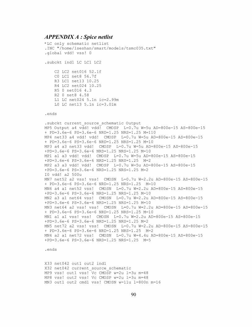
90
APPENDIX A : Spice netlist *LC only schematic netlist .INC "/home/lseshan/smart/models/tsmc035.txt" .global vdd! vss! 0 .subckt ind1 LC LC1 LC2 C2 LC2 net016 52.1f C0 LC1 net8 56.7f R3 LC1 net13 10.25 R4 LC2 net024 10.25 R5 0 net016 4.3 R2 0 net8 4.58 L1 LC net024 5.1n ic=2.99m L0 LC net13 5.1n ic=3.01m .ends .subckt current_source_schematic Output MP5 Output a4 vdd! vdd! CMOSP L=0.7u W=5u AD=800e-15 AS=800e-15 + PD=3.6e-6 PS=3.6e-6 NRD=1.25 NRS=1.25 M=110 MP4 net33 a4 vdd! vdd! CMOSP L=0.7u W=5u AD=800e-15 AS=800e-15 + PD=3.6e-6 PS=3.6e-6 NRD=1.25 NRS=1.25 M=10 MP3 a4 a3 net33 vdd! CMOSP L=0.7u W=5u AD=800e-15 AS=800e-15 +PD=3.6e-6 PS=3.6e-6 NRD=1.25 NRS=1.25 M=10 MP1 a1 a3 vdd! vdd! CMOSP L=0.7u W=5u AD=800e-15 AS=800e-15 +PD=3.6e-6 PS=3.6e-6 NRD=1.25 NRS=1.25 M=2 MP2 a3 a3 vdd! vdd! CMOSP L=0.7u W=5u AD=800e-15 AS=800e-15 +PD=3.6e-6 PS=3.6e-6 NRD=1.25 NRS=1.25 M=2 I0 vdd! a2 500u MN7 net52 a2 vss! vss! CMOSN L=0.7u W=2.2u AD=800e-15 AS=800e-15 + PD=3.6e-6 PS=3.6e-6 NRD=1.25 NRS=1.25 M=10 MN6 a4 a1 net52 vss! CMOSN L=0.7u W=2.2u AD=800e-15 AS=800e-15 +PD=3.6e-6 PS=3.6e-6 NRD=1.25 NRS=1.25 M=10 MN2 a3 a1 net64 vss! CMOSN L=0.7u W=2.2u AD=800e-15 AS=800e-15 +PD=3.6e-6 PS=3.6e-6 NRD=1.25 NRS=1.25 M=10 MN3 net64 a2 vss! vss! CMOSN L=0.7u W=2.2u AD=800e-15 AS=800e-15 + PD=3.6e-6 PS=3.6e-6 NRD=1.25 NRS=1.25 M=10 MN1 a1 a1 vss! vss! CMOSN L=0.7u W=2.2u AD=800e-15 AS=800e-15 +PD=3.6e-6 PS=3.6e-6 NRD=1.25 NRS=1.25 M=2 MN5 net72 a2 vss! vss! CMOSN L=0.7u W=2.2u AD=800e-15 AS=800e-15 + PD=3.6e-6 PS=3.6e-6 NRD=1.25 NRS=1.25 M=2 MN4 a2 a1 net72 vss! CMOSN L=0.7u W=4.4u AD=800e-15 AS=800e-15 +PD=3.6e-6 PS=3.6e-6 NRD=1.25 NRS=1.25 M=5 .ends X33 net042 out1 out2 ind1 X32 net042 current_source_schematic MP9 vss! out1 vss! Vc CMOSP w=2u l=3u m=48 MP8 vss! out2 vss! Vc CMOSP w=2u l=3u m=48 MN3 out1 out2 cmd1 vss! CMOSN w=11u l=800n m=16
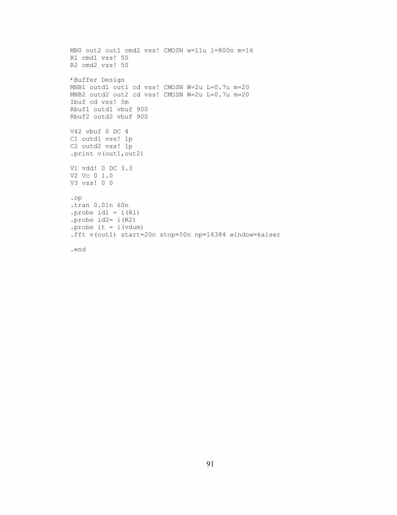
91
MN0 out2 out1 cmd2 vss! CMOSN w=11u l=800n m=16 R1 cmd1 vss! 50 R2 cmd2 vss! 50 *Buffer Design MNB1 outd1 out1 cd vss! CMOSN W=2u L=0.7u m=20 MNB2 outd2 out2 cd vss! CMOSN W=2u L=0.7u m=20 Ibuf cd vss! 5m Rbuf1 outd1 vbuf 900 Rbuf2 outd2 vbuf 900 V42 vbuf 0 DC 4 C1 outd1 vss! 1p C2 outd2 vss! 1p .print v(out1,out2) V1 vdd! 0 DC 3.3 V2 Vc 0 1.0 V3 vss! 0 0 .op .tran 0.01n 60n .probe id1 = i(R1) .probe id2= i(R2) .probe it = i(vdum) .fft v(out1) start=20n stop=50n np=16384 window=kaiser .end
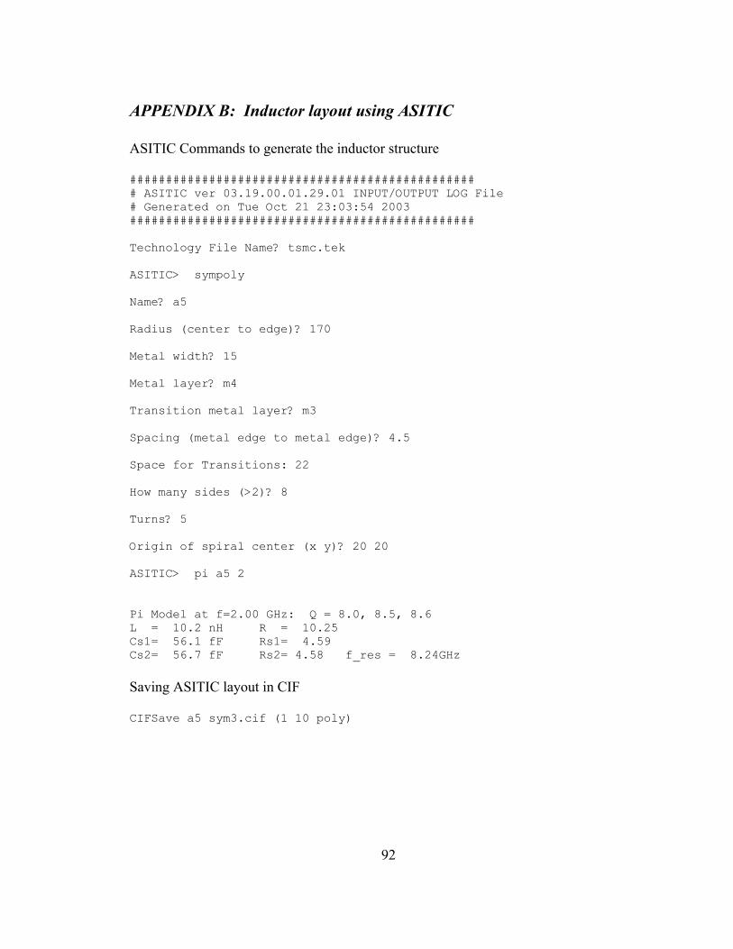
92
APPENDIX B: Inductor layout using ASITIC ASITIC Commands to generate the inductor structure ################################################ # ASITIC ver 03.19.00.01.29.01 INPUT/OUTPUT LOG File # Generated on Tue Oct 21 23:03:54 2003 ################################################ Technology File Name? tsmc.tek ASITIC> sympoly Name? a5 Radius (center to edge)? 170 Metal width? 15 Metal layer? m4 Transition metal layer? m3 Spacing (metal edge to metal edge)? 4.5 Space for Transitions: 22 How many sides (>2)? 8 Turns? 5 Origin of spiral center (x y)? 20 20 ASITIC> pi a5 2 Pi Model at f=2.00 GHz: Q = 8.0, 8.5, 8.6 L = 10.2 nH R = 10.25 Cs1= 56.1 fF Rs1= 4.59 Cs2= 56.7 fF Rs2= 4.58 f_res = 8.24GHz Saving ASITIC layout in CIF CIFSave a5 sym3.cif (1 10 poly)
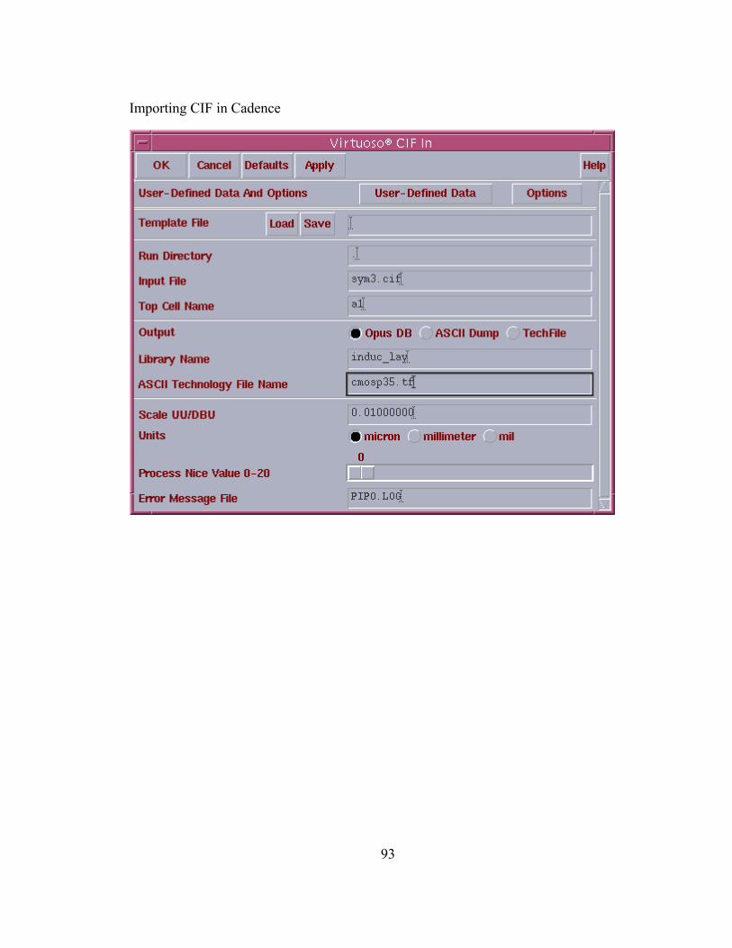
93
Importing CIF in Cadence
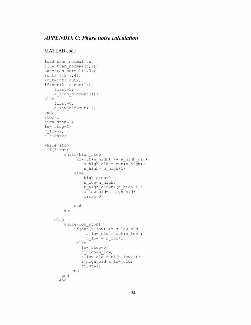
94
APPENDIX C: Phase noise calculation MATLAB code load tran_normal.txt t1 = tran_normal(:,2); out=tran_normal(:,3); %out2=f12(:,4); %out=out1-out2; if(out(2) > out(1)) first=1; a_high_old=out(1); else first=0; a_low_old=out(1); end; stop=1; high_stop=1; low_stop=1; n_low=2; n_high=2; while(stop) if(first) while(high_stop) if(out(n_high) >= a_high_old) a_high_old = out(n_high); n_high= n_high+1; else high_stop=0; n_low=n_high; t_high_old=t1(n_high-1); a_low_old=a_high_old; first=0; end end else while(low_stop) if(out(n_low) <= a_low_old) a_low_old = out(n_low); n_low = n_low+1; else low_stop=0; n_high=n_low; t_low_old = t1(n_low-1); a_high_old=a_low_old; first=1; end end end
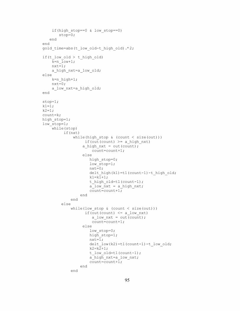
95
if(high_stop==0 & low_stop==0) stop=0; end end gold_time=abs(t_low_old-t_high_old).*2; if(t_low_old > t_high_old) k=n_low+1; nxt=1; a_high_nxt=a_low_old; else k=n_high+1; nxt=0; a_low_nxt=a_high_old; end stop=1; k1=1; k2=1; count=k; high_stop=1; low_stop=1; while(stop) if(nxt) while(high_stop & (count < size(out))) if(out(count) >= a_high_nxt) a_high_nxt = out(count); count=count+1; else high_stop=0; low_stop=1; nxt=0; delt_high(k1)=t1(count-1)-t_high_old; k1=k1+1; t_high_old=t1(count-1); a_low_nxt = a_high_nxt; count=count+1; end end else while(low_stop & (count < size(out))) if(out(count) <= a_low_nxt) a_low_nxt = out(count); count=count+1; else low_stop=0; high_stop=1; nxt=1; delt_low(k2)=t1(count-1)-t_low_old; k2=k2+1; t_low_old=t1(count-1); a_high_nxt=a_low_nxt; count=count+1; end end
96
end if(count > (size(out)-1)) stop=0; end end jitter_high=max(abs(delt_high-gold_time)); jitter_low=max(abs(delt_low-gold_time));
97
VITA Lakshmipriya Seshan was born on the 30th of April 1979 in Trivandrum, India. She
received her high school diploma from All Saints College, Trivandrum in 1996.
Interested in an engineering career, she enrolled at College of Engineering, Trivandrum,
majoring in Electronics and Communication Engineering. In June’ 2000, she graduated
with a Bachelor of Technology degree in Electronics and Communication. She then
began her career in the industry and was employed at Wipro Technologies, Bangalore, as
a VLSI/System Design Engineer, where she worked for a year. In Fall 2001, she enrolled
at the University of Tennessee, Knoxville to earn a Master’s in Electrical Engineering.
She is currently working under the supervision of Dr.Syed K. Islam at the Analog VLSI
and Devices Laboratory. She plans to complete her Master’s with a specialization in
Analog IC design in May 2004.