McKinsey: Executive Summary of the Greece 10 Years Ahead study
A 1-Tap 40-Gbps Look-ahead Decision Feedback Equalizer
in 0.18-μm SiGe BiCMOS Technology
by
Adesh Garg
A thesis submitted in conformity with the requirementsfor the degree of Master of Applied Science
Graduate Department of Electrical and Computer EngineeringUniversity of Toronto
c© Copyright by Adesh Garg 2005
A 1-Tap 40-Gbps Look-ahead Decision Feedback Equalizer
in 0.18-μm SiGe BiCMOS Technology
Adesh Garg
Master of Applied Science, 2005
Graduate Department of Electrical and Computer Engineering
University of Toronto
Abstract
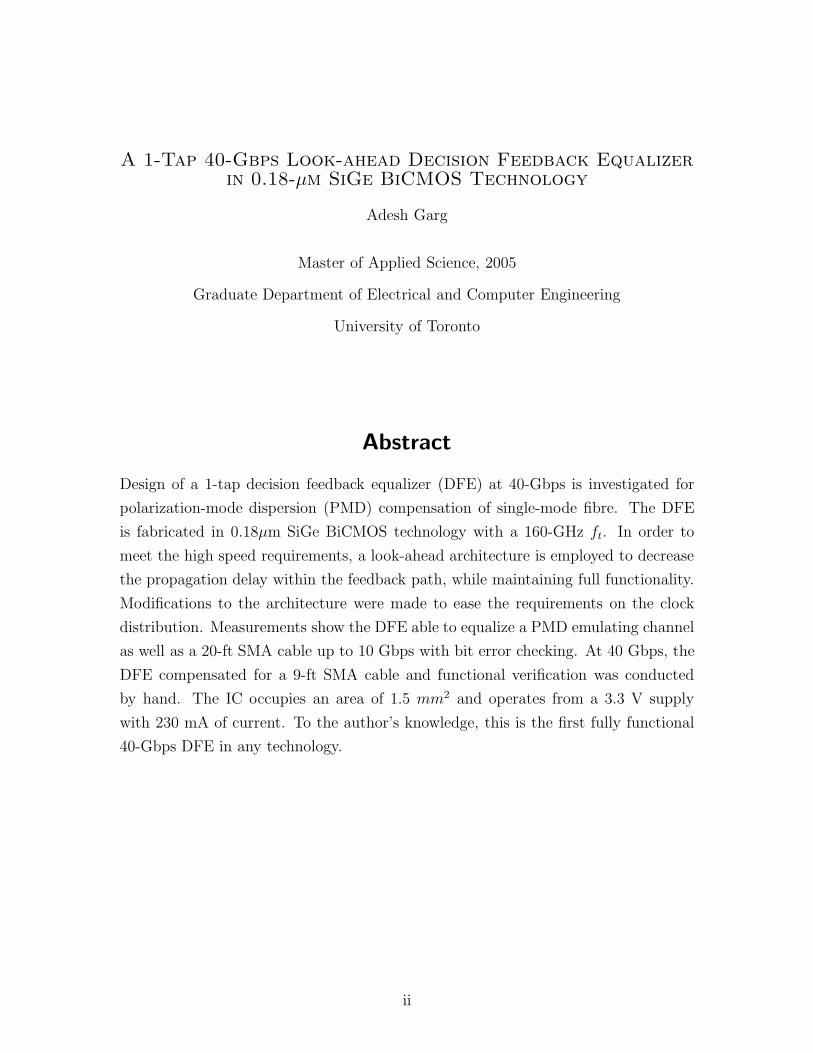
Design of a 1-tap decision feedback equalizer (DFE) at 40-Gbps is investigated for
polarization-mode dispersion (PMD) compensation of single-mode fibre. The DFE
is fabricated in 0.18μm SiGe BiCMOS technology with a 160-GHz ft. In order to
meet the high speed requirements, a look-ahead architecture is employed to decrease
the propagation delay within the feedback path, while maintaining full functionality.
Modifications to the architecture were made to ease the requirements on the clock
distribution. Measurements show the DFE able to equalize a PMD emulating channel
as well as a 20-ft SMA cable up to 10 Gbps with bit error checking. At 40 Gbps, the
DFE compensated for a 9-ft SMA cable and functional verification was conducted
by hand. The IC occupies an area of 1.5 mm2 and operates from a 3.3 V supply
with 230 mA of current. To the author’s knowledge, this is the first fully functional
40-Gbps DFE in any technology.
ii

Acknowledgments
I would like to sincerely thank my supervisors Tony Chan Carusone and Sorin Voinigescu.
Their continued mentorship and support has been staggering over the last two years.
Thank you to Prof. David Johns, Prof. Glenn Gulak, and Prof. Jianwen Zhu for
serving on my thesis examination committee.
Thanks to all the organizations that supported this work in its many forms. Thanks
to NIT, OIT and CFI for test equipment. Grants from the Natural Sciences and Engi-
neering Research Council of Canada (NSERC), Gennum Corporation, and Micronet.
Jazz Semiconductor for fabrication and technology access. And lastly I would like to
acknowledge the CAD tools provided by the Canadian Microelectronics Corporation
(CMC) and supported by Jaro Pristupa.
I would like to thank my friends and fellow graduate students. To Jonathan for
his guidance. To Shahriar for his late night camaraderie. To Tod for simply every-
thing, since there is just too much to list. And lastly to Michael Gordon, may I always
“bathe” in his glory.
To my family who continues to support and love me.
To my love, Anjly, I owe everything.
iii
Contents
List of Figures vi
List of Tables ix
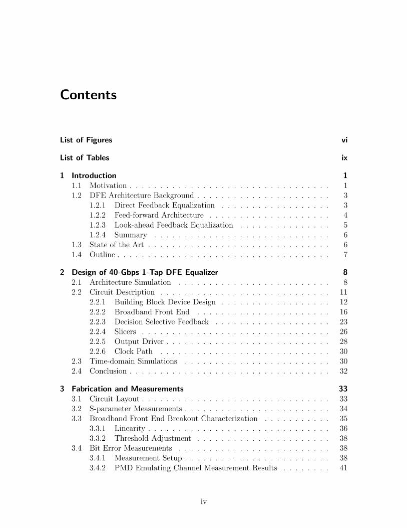
1 Introduction 11.1 Motivation . . . . . . . . . . . . . . . . . . . . . . . . . . . . . . . . . 11.2 DFE Architecture Background . . . . . . . . . . . . . . . . . . . . . . 3
1.2.1 Direct Feedback Equalization . . . . . . . . . . . . . . . . . . 31.2.2 Feed-forward Architecture . . . . . . . . . . . . . . . . . . . . 41.2.3 Look-ahead Feedback Equalization . . . . . . . . . . . . . . . 51.2.4 Summary . . . . . . . . . . . . . . . . . . . . . . . . . . . . . 6
1.3 State of the Art . . . . . . . . . . . . . . . . . . . . . . . . . . . . . . 61.4 Outline . . . . . . . . . . . . . . . . . . . . . . . . . . . . . . . . . . . 7
2 Design of 40-Gbps 1-Tap DFE Equalizer 82.1 Architecture Simulation . . . . . . . . . . . . . . . . . . . . . . . . . 82.2 Circuit Description . . . . . . . . . . . . . . . . . . . . . . . . . . . . 11
2.2.1 Building Block Device Design . . . . . . . . . . . . . . . . . . 122.2.2 Broadband Front End . . . . . . . . . . . . . . . . . . . . . . 162.2.3 Decision Selective Feedback . . . . . . . . . . . . . . . . . . . 232.2.4 Slicers . . . . . . . . . . . . . . . . . . . . . . . . . . . . . . . 262.2.5 Output Driver . . . . . . . . . . . . . . . . . . . . . . . . . . . 282.2.6 Clock Path . . . . . . . . . . . . . . . . . . . . . . . . . . . . 30
2.3 Time-domain Simulations . . . . . . . . . . . . . . . . . . . . . . . . 302.4 Conclusion . . . . . . . . . . . . . . . . . . . . . . . . . . . . . . . . . 32
3 Fabrication and Measurements 333.1 Circuit Layout . . . . . . . . . . . . . . . . . . . . . . . . . . . . . . . 333.2 S-parameter Measurements . . . . . . . . . . . . . . . . . . . . . . . . 343.3 Broadband Front End Breakout Characterization . . . . . . . . . . . 35
3.3.1 Linearity . . . . . . . . . . . . . . . . . . . . . . . . . . . . . . 363.3.2 Threshold Adjustment . . . . . . . . . . . . . . . . . . . . . . 38
3.4 Bit Error Measurements . . . . . . . . . . . . . . . . . . . . . . . . . 383.4.1 Measurement Setup . . . . . . . . . . . . . . . . . . . . . . . . 383.4.2 PMD Emulating Channel Measurement Results . . . . . . . . 41
iv
Contents
3.4.3 20-ft SMA Cable Measurement Results . . . . . . . . . . . . . 413.5 40-Gbps Equalization Measurements . . . . . . . . . . . . . . . . . . 45
3.5.1 Measurement Setup . . . . . . . . . . . . . . . . . . . . . . . . 453.5.2 Measurement Results . . . . . . . . . . . . . . . . . . . . . . . 463.5.3 Measurement Limitation . . . . . . . . . . . . . . . . . . . . . 51
3.6 Summary . . . . . . . . . . . . . . . . . . . . . . . . . . . . . . . . . 52
4 Conclusion and Future Work 54
References 56
v
List of Figures
1.1 Frequency response of PMD with varying γ and Δτ = TB. TB is abit period (e.g. TB = 25 ps at 40 Gbps).[Plot provided by [Sew05]] . 2
1.2 System level view of PMD equalization . . . . . . . . . . . . . . . . . 21.3 Direct feedback equalizer architecture for single tap (solid) and multi-
ple taps (dashed) . . . . . . . . . . . . . . . . . . . . . . . . . . . . . 31.4 Feed-forward architecture of DFE [NNI+04] . . . . . . . . . . . . . . 41.5 1-tap look-ahead feedback equalizer architecture . . . . . . . . . . . . 5
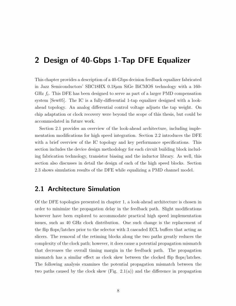
2.1 Look-ahead implementation (a) with retimers at the selector input and(b) with slicers at the selector input . . . . . . . . . . . . . . . . . . . 9
2.2 Monte-Carlo simulation of propagation delay variation through (a) asingle buffer, (b) path 1 with 3 cascaded buffers, (c) path 2 with 3cascaded buffers, and (d) the difference between path 1 and 2 . . . . 11
2.3 Chip block level representation . . . . . . . . . . . . . . . . . . . . . 122.4 Technology figure of merits measurements of ft and fmax and minimum
noise figure at 40 GHz . . . . . . . . . . . . . . . . . . . . . . . . . . 132.5 2-π model of spiral inductor . . . . . . . . . . . . . . . . . . . . . . . 152.6 Inductively peaked amplifier . . . . . . . . . . . . . . . . . . . . . . . 152.7 Single-metal inductor layout . . . . . . . . . . . . . . . . . . . . . . . 172.8 Shunt series feedback amplifier stage . . . . . . . . . . . . . . . . . . 182.9 Sample bit stream showing an unequalized input (top) and slicer out-
put (bottom) for variable slicing threshold (a) Erroneous slicer outputfor zero slicing threshold, α = 0 (b) Error-free slicer output for nonzeroslicing threshold, α �= 0 . . . . . . . . . . . . . . . . . . . . . . . . . 19
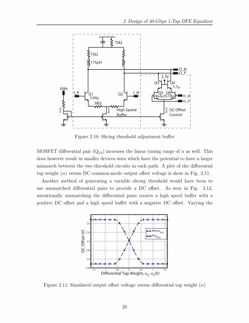
2.10 Slicing threshold adjustment buffer . . . . . . . . . . . . . . . . . . . 202.11 Simulated output offset voltage versus differential tap weight (α) . . . 202.12 Alternative input referred threshold adjustment circuit [GHS+05] . . 212.13 Broadband front end linearity (a) shunt series feedback amplifier (b)
variable slicing threshold buffer . . . . . . . . . . . . . . . . . . . . . 222.14 Simulated single-ended (a) Input/output frequency response for the
TIA and broadband front end (b) noise figure for the TIA, broadbandfront end and the broadband front end with the TIA degenerationresistors shorted . . . . . . . . . . . . . . . . . . . . . . . . . . . . . 23
2.15 ECL schematic (a) selector and (b) MS-FF . . . . . . . . . . . . . . . 242.16 Critical propagation feedback path of DSF . . . . . . . . . . . . . . . 24
vi
List of Figures
2.17 Slicer schematics (3 cascaded ECL buffers) . . . . . . . . . . . . . . . 272.18 Slicer buffer AC frequency response . . . . . . . . . . . . . . . . . . . 282.19 Output driver schematic including the pre-amplifier and output buffer 292.20 Simulated output driver AC frequency response using the prefabrica-
tion and post fabrication design kit . . . . . . . . . . . . . . . . . . . 302.21 Two stage clock buffer schematics . . . . . . . . . . . . . . . . . . . . 312.22 Simulated clock path AC frequency response using the old and updated
design kit . . . . . . . . . . . . . . . . . . . . . . . . . . . . . . . . . 312.23 Simulated single-ended eye diagrams (a) corrupted input eye diagram
through a PMD channel with γ of 0.5 and Δτ of 25 ps (b) equalizedoutput eye diagram . . . . . . . . . . . . . . . . . . . . . . . . . . . . 32
3.1 DFE fabricated in Jazz Semiconductors’ SBC18HX 0.18μm SiGe BiC-MOS technology with a 160-GHz ft operating from a 3.3 V supply with230 mA current. . . . . . . . . . . . . . . . . . . . . . . . . . . . . . . 34
3.2 Broadband front end fabricated in Jazz Semiconductors’ SBC18HX0.18μm SiGe BiCMOS technology with a 160-GHz ft operating froma 3.3 V supply with 30 mA current. . . . . . . . . . . . . . . . . . . . 35
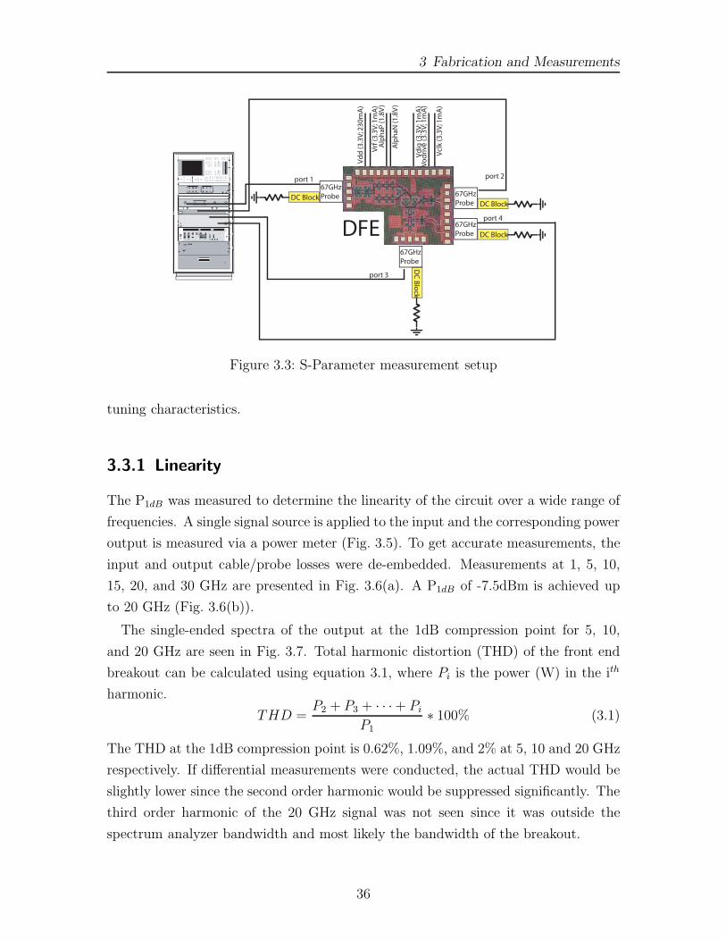
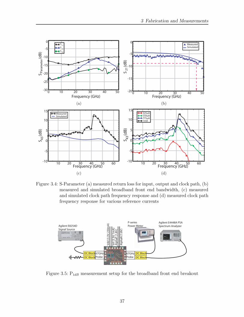
3.3 S-Parameter measurement setup . . . . . . . . . . . . . . . . . . . . . 363.4 S-Parameter (a) measured return loss for input, output and clock path,
(b) measured and simulated broadband front end bandwidth, (c) mea-sured and simulated clock path frequency response and (d) measuredclock path frequency response for various reference currents . . . . . . 37
3.5 P1dB measurement setup for the broadband front end breakout . . . . 373.6 Linearity measurement of the broadband front end breakout (a) P1dB
at 1, 5, 10, 15, 20, and 30 GHz (b) 1dB compression point as a functionof frequency . . . . . . . . . . . . . . . . . . . . . . . . . . . . . . . . 38
3.7 Spectrum of broadband front end at P1dB compression point (a) 5 GHz,(b) 10 GHz and (c) 20 GHz . . . . . . . . . . . . . . . . . . . . . . . 39
3.8 Measured and simulated output offset as a function of differential tun-ing voltage (α) . . . . . . . . . . . . . . . . . . . . . . . . . . . . . . 40
3.9 BERT measurement setup . . . . . . . . . . . . . . . . . . . . . . . . 403.10 BERT measurement schematic setup . . . . . . . . . . . . . . . . . . 423.11 Sample BERT measurement (a) error free and (b) erroneous output . 433.12 Picture of PMD emulating board . . . . . . . . . . . . . . . . . . . . 433.13 Board frequency response . . . . . . . . . . . . . . . . . . . . . . . . 433.14 Input eye diagram through the PMD board at (a) 5-Gbps and (b) 6-Gbps 443.15 Equalized output eye diagram through the PMD board at (a, b) 5-Gbps
and (c, d) 6-Gbps . . . . . . . . . . . . . . . . . . . . . . . . . . . . . 443.16 Channel characteristics over 20-ft SMA cable (a) frequency response
and (b) 10 Gbps 231 − 1 PRBS input eye diagram . . . . . . . . . . . 453.17 10 Gbps equalized output eye diagram through 20-ft SMA cable . . . 453.18 35-40 Gbps measurement test setup . . . . . . . . . . . . . . . . . . . 47
vii
List of Figures
3.19 9-ft SMA cable characteristics (a) frequency response, (b) 231−1 PRBSinput eye at 35 Gbps, (c) 210−1 PRBS input eye at 38 Gbps, (d) 27−1PRBS input eye at 39.5 Gbps . . . . . . . . . . . . . . . . . . . . . . 48
3.20 Single-ended equalized output eye diagram at (a, b) 35-Gbps, (c, d)38-Gbps, (e, f) 39.5-Gbps . . . . . . . . . . . . . . . . . . . . . . . . . 49
3.21 508-bit sequence (27 − 1 PRBS on each board) for an ideal (top), un-equalized (middle) and equalized (bottom) output. Errors indicatedby arrows above bit sequence. . . . . . . . . . . . . . . . . . . . . . . 50
3.22 Jitter measurements for 508-bit sequence at 39.5 Gbps (a) bathtubcurve and (b) jitter histogram . . . . . . . . . . . . . . . . . . . . . . 51
3.23 Single-ended equalized output at 38 Gbps switching between higherorder PRBS patterns (a) 210-1 (b) 223-1 with error . . . . . . . . . . . 52
viii
List of Tables
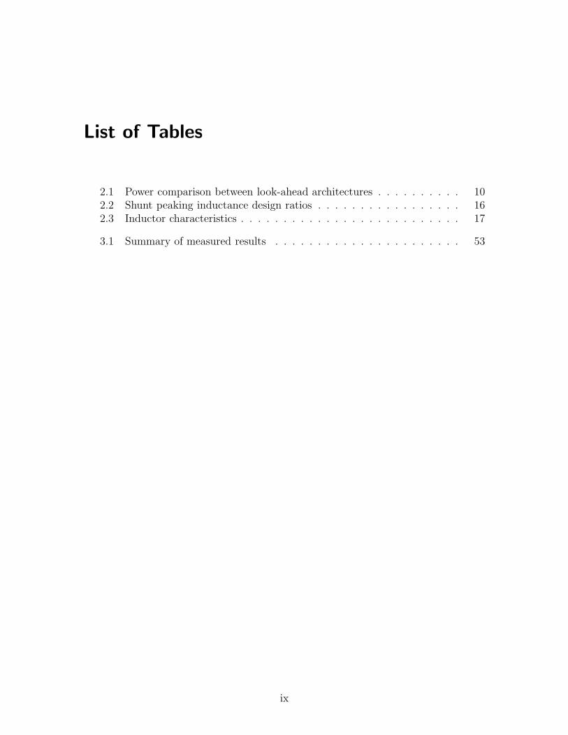
2.1 Power comparison between look-ahead architectures . . . . . . . . . . 102.2 Shunt peaking inductance design ratios . . . . . . . . . . . . . . . . . 162.3 Inductor characteristics . . . . . . . . . . . . . . . . . . . . . . . . . . 17
3.1 Summary of measured results . . . . . . . . . . . . . . . . . . . . . . 53
ix

List of Acronyms
ADC Analog-to-digital converter
AGC Automatic Gain Control
BER Bit error rate
BERT Bit error rate tester
BiCMOS Bipolar complementary metal-oxide semiconductor
CDR Clock and data recovery
CML Current-mode logic
DFE Decision feedback equalizer
DGD Differential group delay
DSF Decision selective feedback
ECL Emitter-coupled logic
EF Emitter follower
FBE Feedback equalizer
FFE Feedforward equalizer
HBT Hetrojunction Bipolar Transistor
IC Integrated circuit
ISI Inter-symbol interference
MOS Metal-oxide semiconductor
OC-768 Optical carrier level 768
PMD Polarization-mode dispersion
SNR Signal-to-noise ratio
TIA Transimpedance Amplifier
x

List of Acronyms
UI Unit interval
VNA Vector Network Analyzer
xi
1 Introduction
1.1 Motivation
As the demand for bandwidth continues to grow, it is only a matter of time before
OC-768 systems will be a common place. The prolonged slow down of the fibre optical
market has allowed researchers to evaluate possible impairments limiting these high
data rate systems. One such impairment identified by [BB04] shows that the long
haul transmission range of single mode fibre systems is limited by polarization-mode
dispersion (PMD). Dispersion compensation of such systems to extend the range of
communication is necessary for industrial adoption of OC-768.
PMD results from the impairments along a fibre optical channel which cause an
input pulse to be split into two pulses with different polarizations. To a first order ap-
proximation, equation 1.1 represents the impulse response of a PMD limited channel
and equation 1.2 presents the corresponding frequency response, where Δτ is the dif-
ferential group delay (DGD) between the two modal pulses and γ is the proportional
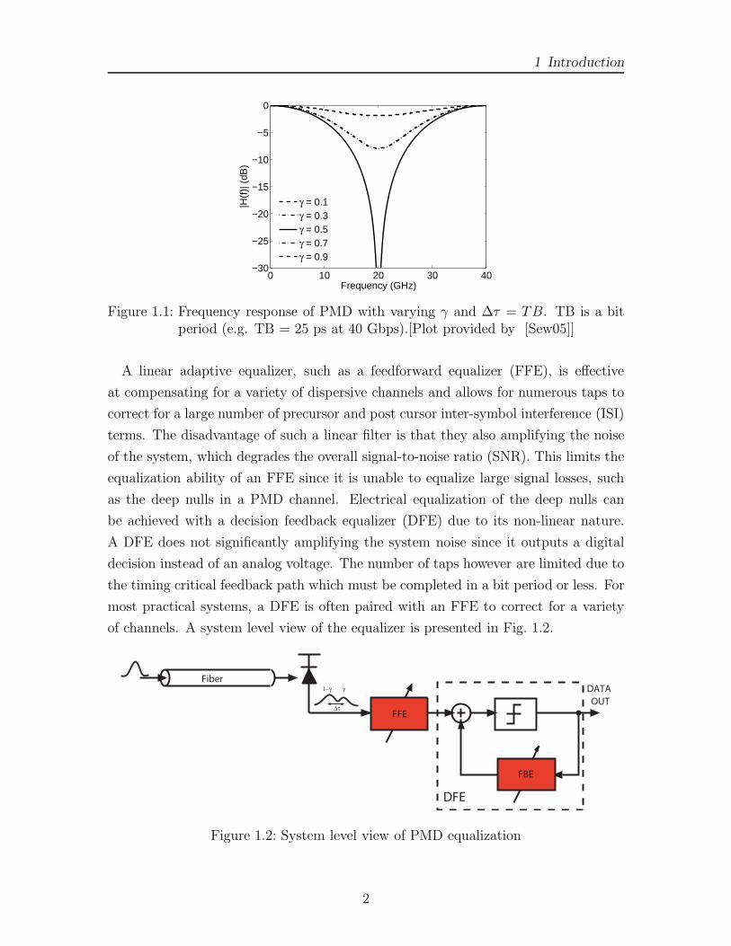
power split. Depending on the DGD and the proportional power split, the frequency
response of the channel changes as seen in Fig. 1.1 for various values of γ. Deep nulls
occur in the frequency response when the proportional power is split evenly between
the two pulses making equalization considerably more difficult.
hpmd(t) = γδ(t) + (1 − γ)δ(t − Δτ) (1.1)
Hpmd(f) = γ + (1 − γ)e−j2πfΔτ (1.2)
Even though PMD compensation can be provided through a variety of means, both
optical and electrical, compelling arguments in [BB04] and [Sew05] push towards an
electrical solution involving an analog adaptive equalizer. An adaptive equalizer is
attractive because it allows for higher levels of system integration and the ability to
adapt to the changing frequency response of a PMD limited system.
1
1 Introduction
0 10 20 30 40−30
−25
−20
−15
−10
−5
0
Frequency (GHz)
|H(f
)| (
dB)
γ = 0.1γ = 0.3γ = 0.5γ = 0.7γ = 0.9
Figure 1.1: Frequency response of PMD with varying γ and Δτ = TB. TB is a bitperiod (e.g. TB = 25 ps at 40 Gbps).[Plot provided by [Sew05]]
A linear adaptive equalizer, such as a feedforward equalizer (FFE), is effective
at compensating for a variety of dispersive channels and allows for numerous taps to
correct for a large number of precursor and post cursor inter-symbol interference (ISI)
terms. The disadvantage of such a linear filter is that they also amplifying the noise
of the system, which degrades the overall signal-to-noise ratio (SNR). This limits the
equalization ability of an FFE since it is unable to equalize large signal losses, such
as the deep nulls in a PMD channel. Electrical equalization of the deep nulls can
be achieved with a decision feedback equalizer (DFE) due to its non-linear nature.
A DFE does not significantly amplifying the system noise since it outputs a digital
decision instead of an analog voltage. The number of taps however are limited due to
the timing critical feedback path which must be completed in a bit period or less. For
most practical systems, a DFE is often paired with an FFE to correct for a variety
of channels. A system level view of the equalizer is presented in Fig. 1.2.
FFE
Fiber DATAOUT
FBE
Δτ
1−γ γ
DFE
Figure 1.2: System level view of PMD equalization
2
1 Introduction
Previous work in [Sew05] shows that a 3-tap FFE paired with a 1-tap feedback
equalizer (FBE) is sufficient to mitigate practical PMD limited systems. This thesis
is a continuation of [Sew05] and involves the design of some of the remaining equalizer
building blocks. This work focuses on the design of a 1-tap 40-Gbps DFE. The scope
of the project involves the implementation of the high speed path and does not address
the adaptation or clock recovery issues.
1.2 DFE Architecture Background
The following sections are a quick overview of the known architectures for DFE im-
plementation. The advantages and disadvantages of each will be examined for high
speed implementation.
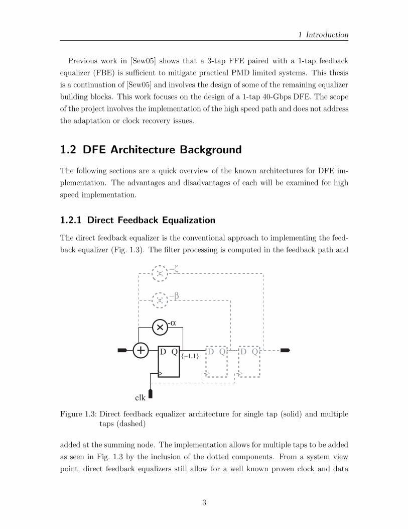
1.2.1 Direct Feedback Equalization
The direct feedback equalizer is the conventional approach to implementing the feed-
back equalizer (Fig. 1.3). The filter processing is computed in the feedback path and
D Q
clk
-α
{−1,1} D Q D Q
−β
−ζ
Figure 1.3: Direct feedback equalizer architecture for single tap (solid) and multipletaps (dashed)
added at the summing node. The implementation allows for multiple taps to be added
as seen in Fig. 1.3 by the inclusion of the dotted components. From a system view
point, direct feedback equalizers still allow for a well known proven clock and data
3
1 Introduction
recovery (CDR) circuit to be used with little added overhead for clock distribution.
The major draw back however involves the timing bottleneck of the feedback path
which must be completed within a bit period, for a baud spaced equalizer. Additional
taps also cause significant loading at the high speed node limiting the performance of
the circuit. Implementation of a direct feedback equalizer at high data rates is lim-
ited. As the fabrication technology improves however, the speed at which the direct
feedback equalizer is viable continues to increase. As will be presented in section 1.3,
current technology has allowed for direct feedback equalizer implementations up to
10 Gbps.
1.2.2 Feed-forward Architecture
An alternate architecture to the direct feedback equalizer is a feed-forward system
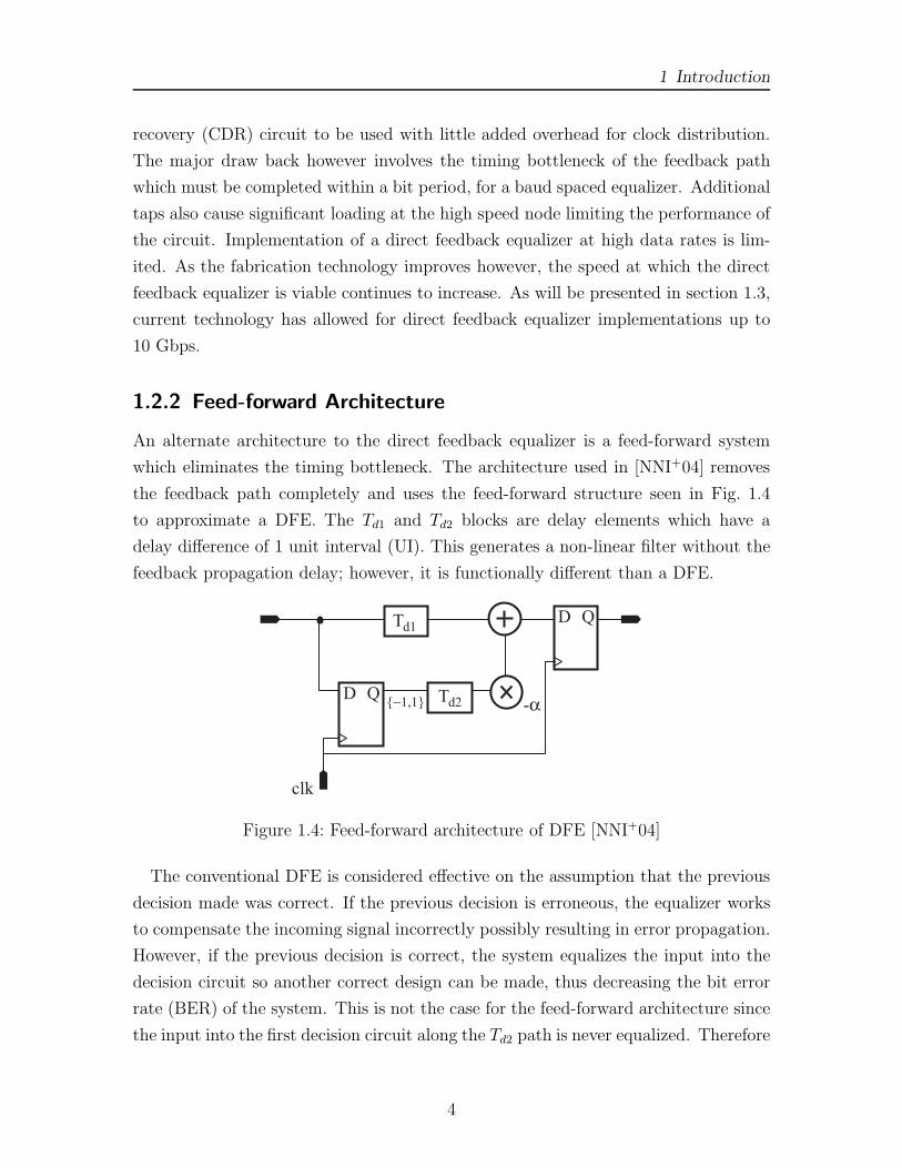
which eliminates the timing bottleneck. The architecture used in [NNI+04] removes
the feedback path completely and uses the feed-forward structure seen in Fig. 1.4
to approximate a DFE. The Td1 and Td2 blocks are delay elements which have a
delay difference of 1 unit interval (UI). This generates a non-linear filter without the
feedback propagation delay; however, it is functionally different than a DFE.
D Q
clk
{−1,1}
D Q
-α
Td1
Td2
Figure 1.4: Feed-forward architecture of DFE [NNI+04]
The conventional DFE is considered effective on the assumption that the previous
decision made was correct. If the previous decision is erroneous, the equalizer works
to compensate the incoming signal incorrectly possibly resulting in error propagation.
However, if the previous decision is correct, the system equalizes the input into the
decision circuit so another correct design can be made, thus decreasing the bit error
rate (BER) of the system. This is not the case for the feed-forward architecture since
the input into the first decision circuit along the Td2 path is never equalized. Therefore
4
1 Introduction
the input into the second decision circuit is equalized based on decisions made from
the input raw BER, thus making error propagation a significant concern. The feed-
forward DFE and the direct DFE are only equivalent if the input raw BER is low, a
case where an equalizer is probably not required. The feed-forward architecture was
not explored further since its functional use was not suitable for this application.
1.2.3 Look-ahead Feedback Equalization
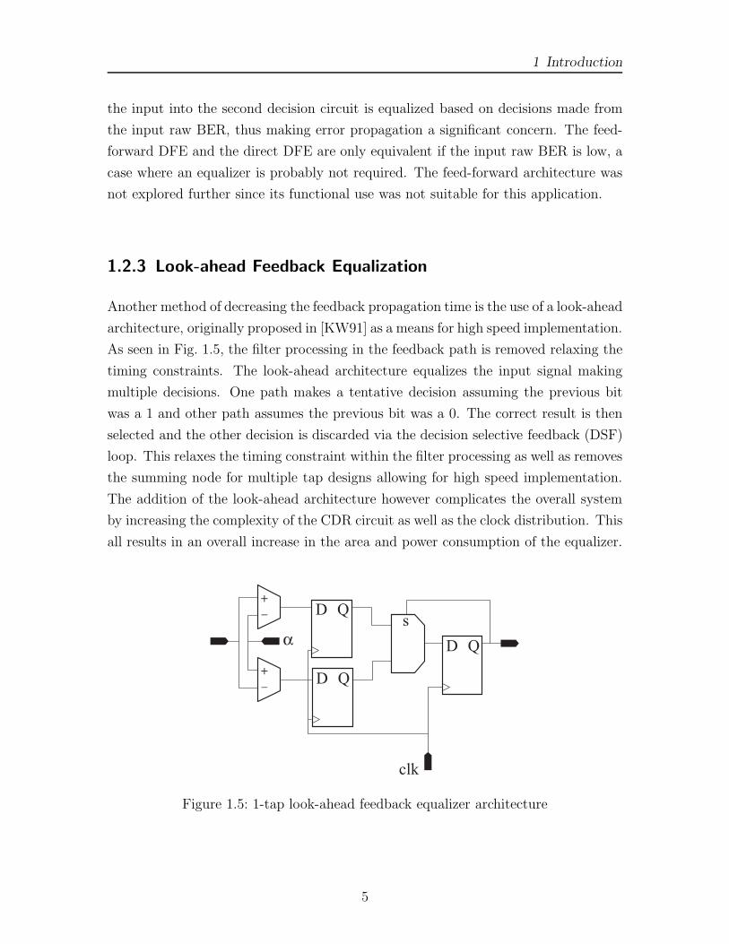
Another method of decreasing the feedback propagation time is the use of a look-ahead
architecture, originally proposed in [KW91] as a means for high speed implementation.
As seen in Fig. 1.5, the filter processing in the feedback path is removed relaxing the
timing constraints. The look-ahead architecture equalizes the input signal making
multiple decisions. One path makes a tentative decision assuming the previous bit
was a 1 and other path assumes the previous bit was a 0. The correct result is then
selected and the other decision is discarded via the decision selective feedback (DSF)
loop. This relaxes the timing constraint within the filter processing as well as removes
the summing node for multiple tap designs allowing for high speed implementation.
The addition of the look-ahead architecture however complicates the overall system
by increasing the complexity of the CDR circuit as well as the clock distribution. This
all results in an overall increase in the area and power consumption of the equalizer.
D Qs
clk
D Q
D Q
α
+_
+_
Figure 1.5: 1-tap look-ahead feedback equalizer architecture
5
1 Introduction
1.2.4 Summary
The look-ahead architecture has the advantage of relaxed timing constraints in the
feedback path while maintaining full functionality. Disadvantages of the look-ahead
architecture do pose system level issues, however solutions are available [SHG+04]
[KHB97]. More details of the system architecture will be presented in section 2.1.
1.3 State of the Art
Since DFEs have been identified as a useful and necessary addition to adaptive equal-
izers for systems in the gigabit regime, considerable work has recently emerged. The
following is a survey of the state of the art implemented adaptive equalizers cir-
cuits, which service a host of applications including chip-to-chip, backplane and mul-
timode/single mode fibre.
Texas Instruments presented a 6.25-Gpbs adaptive 4-tap DFE for serial backplane
communication [PBR+05]. The tap spacing is a half UI and allows direct first post-
cursor cancellation using a direct feedback architecture. The IC was fabricated in a
0.13μm CMOS process occupying an area of 0.24 mm2 and consumed 180mW from
a 1.2 V supply.
Vitesse Semiconductor published a binary transceiver with adaptive equalizer for
backplane transmission operating at 5-Gbps [KBPC+05]. It consisted of a 1-Tap FFE
and a 3-tap feedback equalizer at the receiver. The entire transceiver occupied an
area of 12 mm2 in 0.12μm CMOS technology. It consumed 2.1 W of power from 1.2 V
supply. The DFE was implemented using a direct feedback architecture.
Synopsys, Stexar and UNC all presented a joint paper [KYMW+05] which intro-
duced a 0.6 to 9.6-Gbps transceiver with both transmit and receive side equalization.
Fabricated in 0.13μm CMOS technology occupying an area of 0.56 mm2 and con-
sumes 150 mW at 6.25-Gbps. The transmit equalizer has fixed 3-tap weights and the
receive side equalizer has a 1-tap look-ahead DFE.
IBM published a 6.4-Gbps 0.13μm CMOS SerDes Core with a 4-tap feed-forward
and 5-tap feedback equalizer [SBS+05]. The DFE used a look-ahead architecture for
the first tap and a direct feedback for taps 2 through 5. The combination was able to
compensate for loses over 30 dB. The transceiver consumed 290mW from 1.2V supply
with an area of 0.79mm2.
Bulow, et al. presented a 10-Gbps DFE [BBB+00], consisting of an 8-tap (55 ps
6
1 Introduction
tap spacing) FFE and a 1-tap FBE was implemented in a SiGe process. The feedback
equalizer was implemented using a look-ahead architecture and could compensate for
PMD up to 1-bit of DGD.
Quake Technologies Inc [MTP05] introduced a 10-Gbps equalizer for single mode
fibre with clock and data recovery and on-chip adaptation. The equalizer is a 9-tap
FFE with a 3-tap DFE. The system was implemented in a SiGe BiCMOS processes
and occupies and area of 9 mm2. The circuit consumes 900mW.
The fastest non-linear equalizer to the author’s knowledge was presented in [NNI+04],
by a group at NTT Photonics Laboratories. The IC uses a 1-tap feed-forward architec-
ture to approximate a DFE operates at 40-Gbps. It was fabricated in a InP/InGaAs
HBT technology with an ft of 150 GHz occupying an area of 4 mm2. It operated from
a -4.5 V supply consuming 1.3 W of power. Measurements showed it was effective in
mitigating PMD with Δτ of 25 ps and a γ of 0.3 at 40-Gbps.
Some researchers have proposed digital solutions for equalizing these high speed
channels. The NTT Photonics Laboratories, who published the fastest DFE, also
published a 10-Gbps digital equalizer solution for multimode fibre compensation
[NNS+05]. A 24-Gsps, 3-bit analog-to-digital converter (ADC) was used to sam-
ple 10-Gbps data and equalize PMD within a fibre channel. The chip size for the
ADC was 9 mm2, with a power consumption of 3.84 W from a 4 V supply. These
digital solution including other ADCs, are not practical for most systems due to the
extremely high power consumption and chip size. Given current technology and speed
limitations, ADC solutions are far from being viable at these speeds.
1.4 Outline
The rest of the thesis is outlined as follows. Chapter 2 contains a discussion of the
various circuit blocks designed and the high speed implementation issues involved.
Chapter 3 contains measurement results and the characterization of the DFE. Chapter
4 provides conclusions and a discussion of future research opportunities.
7
2 Design of 40-Gbps 1-Tap DFE Equalizer
This chapter provides a description of a 40-Gbps decision feedback equalizer fabricated
in Jazz Semiconductors’ SBC18HX 0.18μm SiGe BiCMOS technology with a 160-
GHz ft. This DFE has been designed to serve as part of a larger PMD compensation
system [Sew05]. The IC is a fully-differential 1-tap equalizer designed with a look-
ahead topology. An analog differential control voltage adjusts the tap weight. On
chip adaptation or clock recovery were beyond the scope of this thesis, but could be
accommodated in future work.
Section 2.1 provides an overview of the look-ahead architecture, including imple-
mentation modifications for high speed integration. Section 2.2 introduces the DFE
with a brief overview of the IC topology and key performance specifications. This
section includes the device design methodology for each circuit building block includ-
ing fabrication technology, transistor biasing and the inductor library. As well, this
section also discusses in detail the design of each of the high speed blocks. Section
2.3 shows simulation results of the DFE while equalizing a PMD channel model.
2.1 Architecture Simulation
Of the DFE topologies presented in chapter 1, a look-ahead architecture is chosen in
order to minimize the propagation delay in the feedback path. Slight modifications
however have been explored to accommodate practical high speed implementation
issues, such as 40 GHz clock distribution. One such change is the replacement of
the flip flops/latches prior to the selector with 3 cascaded ECL buffers that acting as
slicers. The removal of the retiming blocks along the two paths greatly reduces the
complexity of the clock path; however, it does cause a potential propagation mismatch
that decreases the overall timing margin in the feedback path. The propagation
mismatch has a similar effect as clock skew between the clocked flip flops/latches.
The following analysis examines the potential propagation mismatch between the
two paths caused by the clock skew (Fig. 2.1(a)) and the difference in propagation
8
2 Design of 40-Gbps 1-Tap DFE Equalizer
delay between the slicers (Fig. 2.1(b)).
D Qs
clk
α
+_
+_
Rf D Q
D Q
DUMMY
(a)
D Qs
clk
α
+_
+_
Path 1
Path 2
(b)
Figure 2.1: Look-ahead implementation (a) with retimers at the selector input and(b) with slicers at the selector input
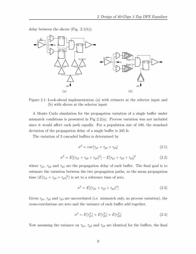
A Monte Carlo simulation for the propagation variation of a single buffer under
mismatch conditions is presented in Fig 2.2(a). Process variation was not included
since it would affect each path equally. For a population size of 100, the standard
deviation of the propagation delay of a single buffer is 345 fs.
The variation of 3 cascaded buffers is determined by
σ2 = var[τp1 + τp2 + τp3] (2.1)
σ2 = E[(τp1 + τp2 + τp3)2] − E[τp1 + τp2 + τp3]
2 (2.2)
where τp1, τp2 and τp3 are the propagation delay of each buffer. The final goal is to
estimate the variation between the two propagation paths, so the mean propagation
time (E[τp1 + τp2 + τp3]2) is set to a reference time of zero.
σ2 = E[(τp1 + τp2 + τp3)2] (2.3)
Given τp1, τp2 and τp3 are uncorrelated (i.e. mismatch only, no process variation), the
cross-correlations are zero and the variance of each buffer add together.
σ2 = E[τ 2p1] + E[τ 2
p2] + E[τ 2p3] (2.4)
Now assuming the variance on τp1, τp2 and τp3 are identical for the buffers, the final
9
2 Design of 40-Gbps 1-Tap DFE Equalizer
relationship is
σ3 =√
3σ1 (2.5)
From Fig. 2.2(b)-(c), the simulation corresponds for a population size of 100 with a
σ of 550fs for path 1 and 480fs for path 2. A similar derivation can be made for the
propagation variation between the two asynchronous paths and the variation in the
clock distribution, found in equation 2.6 and 2.7 respectively.
σtpmismatch =√
var[τp1 + τp2 + τp3 − τp4 − τp5 − τp6] =√
6σ1 (2.6)
σtpclock =√
var[τp1 + τp2 − τp3 − τp4] =√
4σ1 (2.7)
This results in 22% less variation in the clock distribution than the asynchronous
path, not including the physical routing of the clock which makes the mismatch on
the clock path optimistic. The slicer implementation has a possible mismatch of
approximately 845 fs for one standard deviation. To verify the theoretical value and
the assumptions above, a Monte Carlo simulation (Fig. 2.2(d)) for the implemented
slicers (Section 2.2.4) shows a variation of 680 fs.
With respect to power consumption, there is a significant difference between the two
architectures. Estimating the power consumption, using a buffer power of 26.4 mW,
a latch power of 68 mW, and a clock buffer power of 59 mW; the resulting power
difference is 278 mW in favor of the slicer based look-ahead architecture (Table 2.1).
The estimated powers of the buffer, latch and clock buffer include emitter followers.
Table 2.1: Power comparison between look-ahead architecturesArchitecture Data Power Clock Power
Look-ahead with Slicers 158.4 mW 120 mWLook-ahead with Flip Flops 136 mW 420 mW
Though it is shown that the retimed selector inputs would provide a more robust
circuit implementation, the reduction in power and circuit complexity provides favor-
able trade-offs. The slicer bases look-ahead DFE was implemented.
10
2 Design of 40-Gbps 1-Tap DFE Equalizer
Propogation Variationof a Single Buffer
Propogation VariationThrough Path 1
Propogation VariationThrough Path 2
Propogation DifferenceBetween Path 1 & 2
mean = 165.35psstd = 345.9fsN = 100
mean = 153.6psstd = 553fsN = 100
mean = 153.6psstd = 481.9fsN = 100
mean = 36.6fsstd = 679fsN = 100
(a)
(c)
(b)
(d)
Figure 2.2: Monte-Carlo simulation of propagation delay variation through (a) a sin-gle buffer, (b) path 1 with 3 cascaded buffers, (c) path 2 with 3 cascadedbuffers, and (d) the difference between path 1 and 2
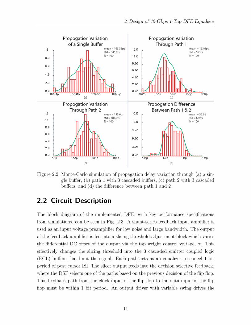
2.2 Circuit Description
The block diagram of the implemented DFE, with key performance specifications
from simulations, can be seen in Fig. 2.3. A shunt-series feedback input amplifier is
used as an input voltage preamplifier for low noise and large bandwidth. The output
of the feedback amplifier is fed into a slicing threshold adjustment block which varies
the differential DC offset of the output via the tap weight control voltage, α. This
effectively changes the slicing threshold into the 3 cascaded emitter coupled logic
(ECL) buffers that limit the signal. Each path acts as an equalizer to cancel 1 bit
period of post cursor ISI. The slicer output feeds into the decision selective feedback,
where the DSF selects one of the paths based on the previous decision of the flip flop.
This feedback path from the clock input of the flip flop to the data input of the flip
flop must be within 1 bit period. An output driver with variable swing drives the
11
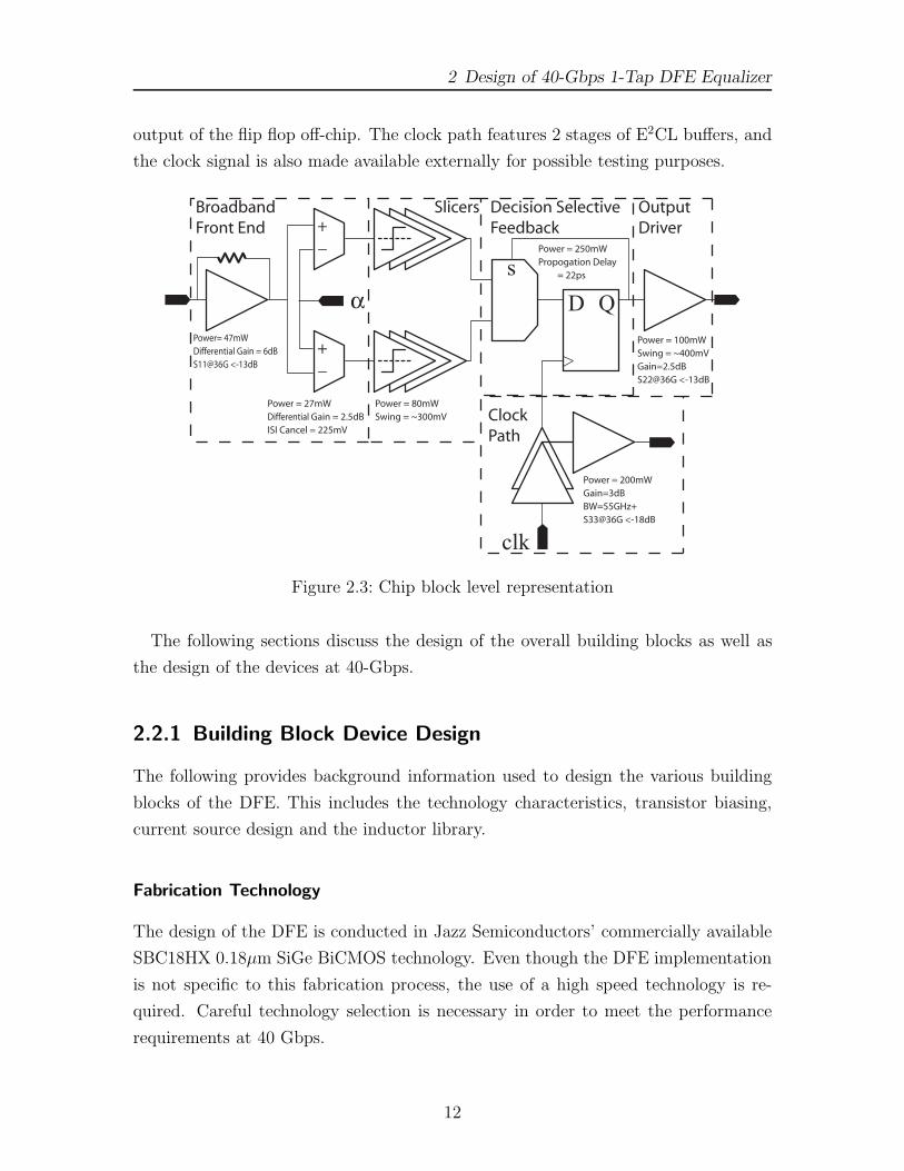
2 Design of 40-Gbps 1-Tap DFE Equalizer
output of the flip flop off-chip. The clock path features 2 stages of E2CL buffers, and
the clock signal is also made available externally for possible testing purposes.
D Qs
clk
αPower= 47mWDifferential Gain = 6dBS11@36G <-13dB
Power = 27mWDifferential Gain = 2.5dBISI Cancel = 225mV
Power = 80mWSwing = ~300mV
Power = 250mWPropogation Delay = 22ps
Power = 100mWSwing = ~400mVGain=2.5dBS22@36G <-13dB
Power = 200mWGain=3dBBW=55GHz+S33@36G <-18dB
+_
+_
BroadbandFront End
ClockPath
Decision SelectiveFeedback
Slicers OutputDriver
Figure 2.3: Chip block level representation
The following sections discuss the design of the overall building blocks as well as
the design of the devices at 40-Gbps.
2.2.1 Building Block Device Design
The following provides background information used to design the various building
blocks of the DFE. This includes the technology characteristics, transistor biasing,
current source design and the inductor library.
Fabrication Technology
The design of the DFE is conducted in Jazz Semiconductors’ commercially available
SBC18HX 0.18μm SiGe BiCMOS technology. Even though the DFE implementation
is not specific to this fabrication process, the use of a high speed technology is re-
quired. Careful technology selection is necessary in order to meet the performance
requirements at 40 Gbps.
12
2 Design of 40-Gbps 1-Tap DFE Equalizer
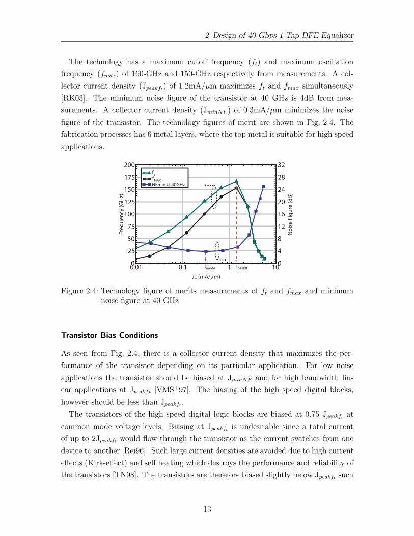
The technology has a maximum cutoff frequency (ft) and maximum oscillation
frequency (fmax) of 160-GHz and 150-GHz respectively from measurements. A col-
lector current density (Jpeakft) of 1.2mA/μm maximizes ft and fmax simultaneously
[RK03]. The minimum noise figure of the transistor at 40 GHz is 4dB from mea-
surements. A collector current density (JminNF ) of 0.3mA/μm minimizes the noise
figure of the transistor. The technology figures of merit are shown in Fig. 2.4. The
fabrication processes has 6 metal layers, where the top metal is suitable for high speed
applications.
0.01 0.1 10
Jc (mA/μm)
0
25
50
75
100
125
150
175
200
Freq
uen
cy (G
Hz)
0
4
8
12
16
20
24
28
32
No
ise
Fig
ure
(dB
)
1
NFmin @ 40GHz
fMAX
ft
JminNF Jpeakft
Figure 2.4: Technology figure of merits measurements of ft and fmax and minimumnoise figure at 40 GHz
Transistor Bias Conditions
As seen from Fig. 2.4, there is a collector current density that maximizes the per-
formance of the transistor depending on its particular application. For low noise
applications the transistor should be biased at JminNF and for high bandwidth lin-
ear applications at Jpeakft [VMS+97]. The biasing of the high speed digital blocks,
however should be less than Jpeakft.
The transistors of the high speed digital logic blocks are biased at 0.75 Jpeakft at
common mode voltage levels. Biasing at Jpeakft is undesirable since a total current
of up to 2Jpeakft would flow through the transistor as the current switches from one
device to another [Rei96]. Such large current densities are avoided due to high current
effects (Kirk-effect) and self heating which destroys the performance and reliability of
the transistors [TN98]. The transistors are therefore biased slightly below Jpeakft such
13
2 Design of 40-Gbps 1-Tap DFE Equalizer
that it operates within the top portion of the ft curves (Fig. 2.4) during switching
[Voi05]. Lower current densities are not used due to the performance degradation of
the blocks.
For an emitter follower (EF), the transistor is biased between 1/2 to 1/3 Jpeakft. The
devices are typically not be biased at peak ft due to the overshoot in the frequency
response [Voi05]. It can be shown that the small signal voltage transfer function is a 2
pole system which can potentially be underdamped [JM97]. Biasing the EF at lower
Jpeakft still provides the required bandwidth while minimizing the potential peaking.
Current Sources
The current sources of the building blocks are all simple MOSFET current mirrors.
More complicated current mirror topologies are not employed to increase the output
impedance, and hence the common-mode rejection, since at high frequencies the
capacitance dominates. Degenerated bipolar transistors typically are better suited
for use as current sources due to their high output impedance and low collector-
substrate capacitance; however, to allow for operation from a lower power supply
voltage, MOSFET current sources were used throughout the design.
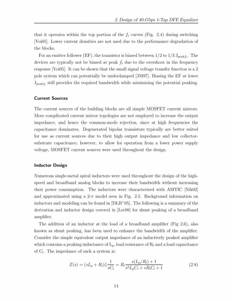
Inductor Design
Numerous single-metal spiral inductors were used throughout the design of the high-
speed and broadband analog blocks to increase their bandwidth without increasing
their power consumption. The inductors were characterized with ASITIC [Nik02]
and approximated using a 2-π model seen in Fig. 2.5. Background information on
inductors and modeling can be found in [DLB+05]. The following is a summary of the
derivation and inductor design covered in [Lee98] for shunt peaking of a broadband
amplifier.
The addition of an inductor at the load of a broadband amplifier (Fig 2.6), also
known as shunt peaking, has been used to enhance the bandwidth of the amplifier.
Consider the simple equivalent output impedance of an inductively peaked amplifier
which contains a peaking inductance of Lp, load resistance of Rl and a load capacitance
of Cl. The impedance of such a system is:
Z(s) = (sLp + Rl)|| 1
sCl
= Rls(Lp/Rl) + 1
s2LpCl + sRlCl + 1(2.8)
14
2 Design of 40-Gbps 1-Tap DFE Equalizer
Figure 2.5: 2-π model of spiral inductor
The addition of the inductor increases the bandwidth by introducing a zero to the
Lp
RlCl
Figure 2.6: Inductively peaked amplifier
transfer function as well as increasing the frequency at which the pole has an effect.
The bandwidth enhancement, where ω2 is the “peaked” bandwidth and ω1 is the
previous bandwidth, is given in equation 2.9. The passive elements are collected such
that m = R2C/L.
ω2
ω1=
√(−m2
2+ m + 1) +
√(−m2
2+ m + 1)2 + m2 (2.9)
Using this equation, design guidelines are set to help choose the correct m ratio.
From results in [Lee98], the following table is obtained. All inductors were designed
to not exceed the group delay requirements so as to not add jitter to the broadband
data. Thus by employing inductive peaking, a 60% improvement in bandwidth can
15
2 Design of 40-Gbps 1-Tap DFE Equalizer
be obtained without increasing power consumption.
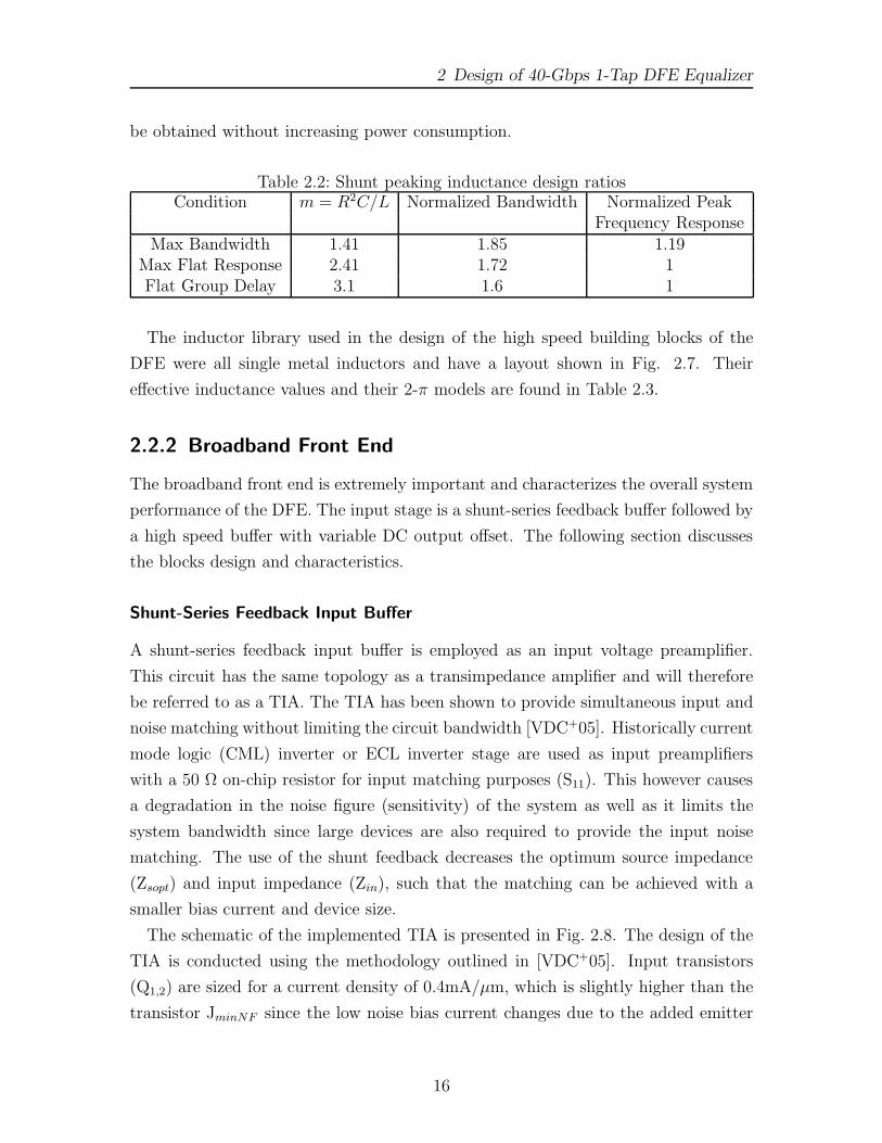
Table 2.2: Shunt peaking inductance design ratiosCondition m = R2C/L Normalized Bandwidth Normalized Peak
Frequency ResponseMax Bandwidth 1.41 1.85 1.19
Max Flat Response 2.41 1.72 1Flat Group Delay 3.1 1.6 1
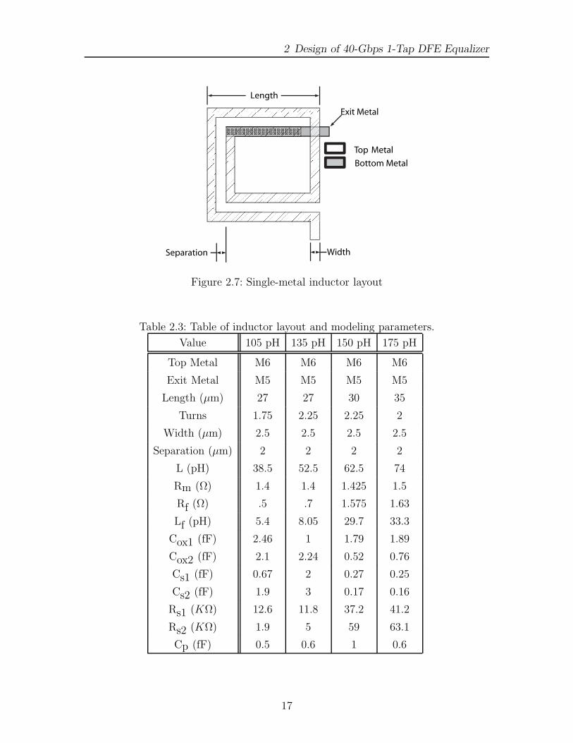
The inductor library used in the design of the high speed building blocks of the
DFE were all single metal inductors and have a layout shown in Fig. 2.7. Their
effective inductance values and their 2-π models are found in Table 2.3.
2.2.2 Broadband Front End
The broadband front end is extremely important and characterizes the overall system
performance of the DFE. The input stage is a shunt-series feedback buffer followed by
a high speed buffer with variable DC output offset. The following section discusses
the blocks design and characteristics.
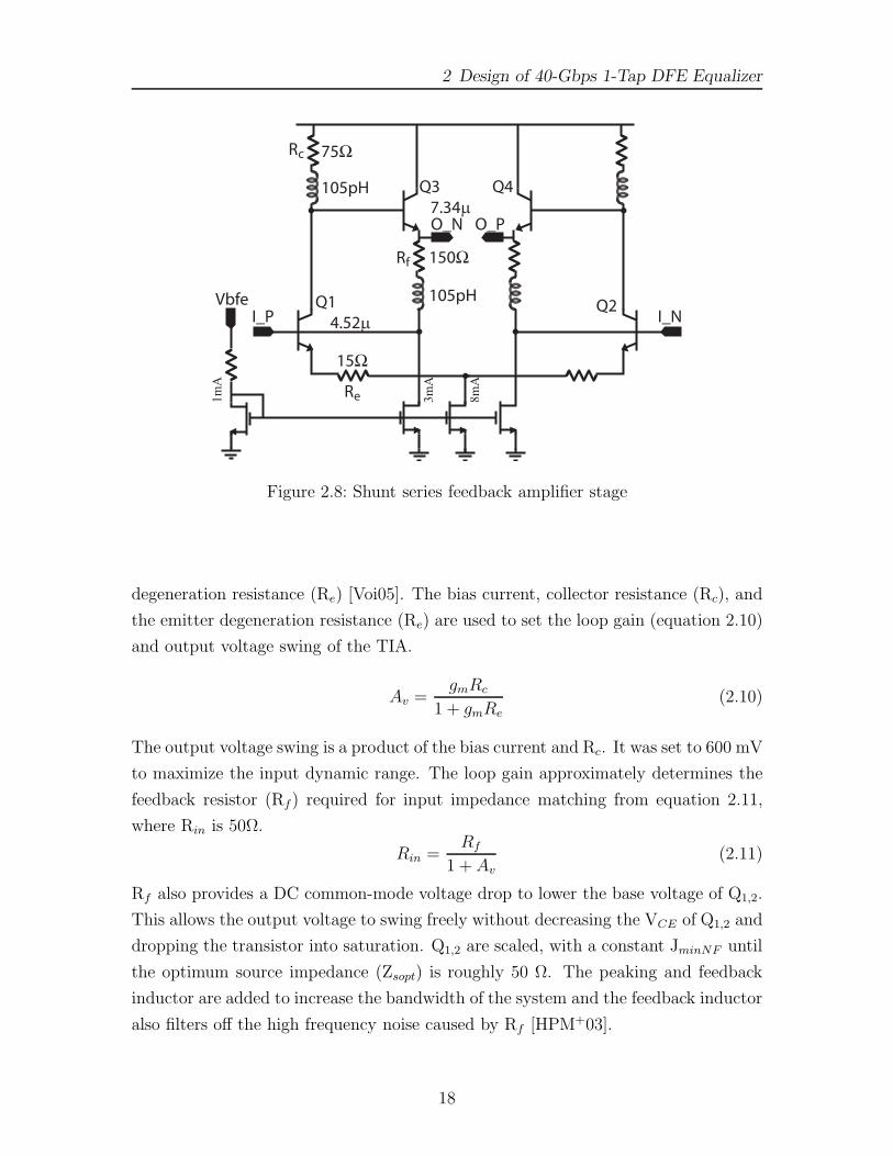
Shunt-Series Feedback Input Buffer
A shunt-series feedback input buffer is employed as an input voltage preamplifier.
This circuit has the same topology as a transimpedance amplifier and will therefore
be referred to as a TIA. The TIA has been shown to provide simultaneous input and
noise matching without limiting the circuit bandwidth [VDC+05]. Historically current
mode logic (CML) inverter or ECL inverter stage are used as input preamplifiers
with a 50 Ω on-chip resistor for input matching purposes (S11). This however causes
a degradation in the noise figure (sensitivity) of the system as well as it limits the
system bandwidth since large devices are also required to provide the input noise
matching. The use of the shunt feedback decreases the optimum source impedance
(Zsopt) and input impedance (Zin), such that the matching can be achieved with a
smaller bias current and device size.
The schematic of the implemented TIA is presented in Fig. 2.8. The design of the
TIA is conducted using the methodology outlined in [VDC+05]. Input transistors
(Q1,2) are sized for a current density of 0.4mA/μm, which is slightly higher than the
transistor JminNF since the low noise bias current changes due to the added emitter
16
2 Design of 40-Gbps 1-Tap DFE Equalizer
Separation Width
Top Metal
Bottom Metal
Length
Exit Metal
Figure 2.7: Single-metal inductor layout
Table 2.3: Table of inductor layout and modeling parameters.
Value 105 pH 135 pH 150 pH 175 pH
Top Metal M6 M6 M6 M6
Exit Metal M5 M5 M5 M5
Length (μm) 27 27 30 35
Turns 1.75 2.25 2.25 2
Width (μm) 2.5 2.5 2.5 2.5
Separation (μm) 2 2 2 2
L (pH) 38.5 52.5 62.5 74
Rm (Ω) 1.4 1.4 1.425 1.5
Rf (Ω) .5 .7 1.575 1.63
Lf (pH) 5.4 8.05 29.7 33.3
Cox1 (fF) 2.46 1 1.79 1.89
Cox2 (fF) 2.1 2.24 0.52 0.76
Cs1 (fF) 0.67 2 0.27 0.25
Cs2 (fF) 1.9 3 0.17 0.16
Rs1 (KΩ) 12.6 11.8 37.2 41.2
Rs2 (KΩ) 1.9 5 59 63.1
Cp (fF) 0.5 0.6 1 0.6
17
2 Design of 40-Gbps 1-Tap DFE Equalizer
75Ω
150Ω
105pH
105pH
15Ω
3mA
8mA
Q1 4.52μ
Q2
Q3 7.34μ
Q4
1mA
Vbfe
Re
Rc
Rf
I_P I_N
O_N O_P
Figure 2.8: Shunt series feedback amplifier stage
degeneration resistance (Re) [Voi05]. The bias current, collector resistance (Rc), and
the emitter degeneration resistance (Re) are used to set the loop gain (equation 2.10)
and output voltage swing of the TIA.
Av =gmRc
1 + gmRe
(2.10)
The output voltage swing is a product of the bias current and Rc. It was set to 600 mV
to maximize the input dynamic range. The loop gain approximately determines the
feedback resistor (Rf) required for input impedance matching from equation 2.11,
where Rin is 50Ω.
Rin =Rf
1 + Av(2.11)
Rf also provides a DC common-mode voltage drop to lower the base voltage of Q1,2.
This allows the output voltage to swing freely without decreasing the VCE of Q1,2 and
dropping the transistor into saturation. Q1,2 are scaled, with a constant JminNF until
the optimum source impedance (Zsopt) is roughly 50 Ω. The peaking and feedback
inductor are added to increase the bandwidth of the system and the feedback inductor
also filters off the high frequency noise caused by Rf [HPM+03].
18
2 Design of 40-Gbps 1-Tap DFE Equalizer
Slicing Threshold Adjustment Buffer
The slicing threshold adjustment buffer (Fig. 2.10) is composed of an emitter degen-
erated high-speed bipolar stage with DC common-mode offset control of the outputs
(OP/N) using a BiCMOS cascode (Q3,4,5,6) via a control voltage, α. This circuit is
the physical implementation of the filter coefficients of the equalizer. An introduction
of a common-mode offset at the outputs causes a nonzero slicing threshold into the
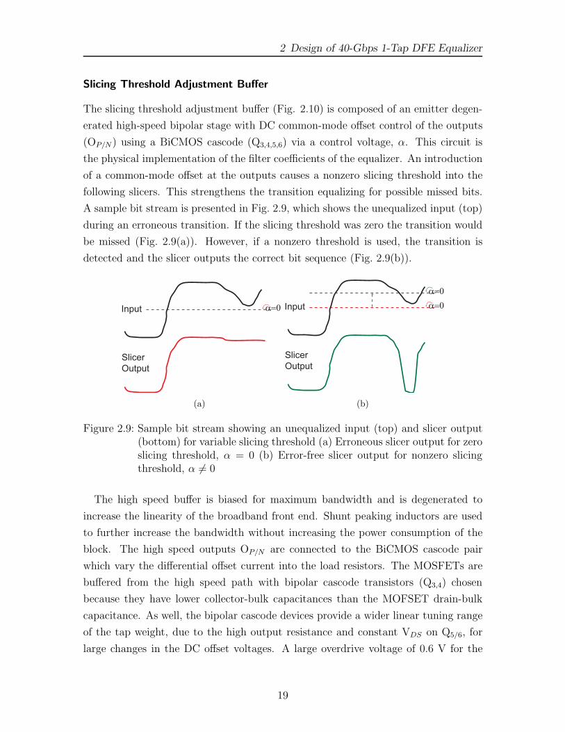
following slicers. This strengthens the transition equalizing for possible missed bits.
A sample bit stream is presented in Fig. 2.9, which shows the unequalized input (top)
during an erroneous transition. If the slicing threshold was zero the transition would
be missed (Fig. 2.9(a)). However, if a nonzero threshold is used, the transition is
detected and the slicer outputs the correct bit sequence (Fig. 2.9(b)).
α=0Input
SlicerOutput
(a)
α=0
α=0
Input
SlicerOutput
(b)
Figure 2.9: Sample bit stream showing an unequalized input (top) and slicer output(bottom) for variable slicing threshold (a) Erroneous slicer output for zeroslicing threshold, α = 0 (b) Error-free slicer output for nonzero slicingthreshold, α �= 0
The high speed buffer is biased for maximum bandwidth and is degenerated to
increase the linearity of the broadband front end. Shunt peaking inductors are used
to further increase the bandwidth without increasing the power consumption of the
block. The high speed outputs OP/N are connected to the BiCMOS cascode pair
which vary the differential offset current into the load resistors. The MOSFETs are
buffered from the high speed path with bipolar cascode transistors (Q3,4) chosen
because they have lower collector-bulk capacitances than the MOFSET drain-bulk
capacitance. As well, the bipolar cascode devices provide a wider linear tuning range
of the tap weight, due to the high output resistance and constant VDS on Q5/6, for
large changes in the DC offset voltages. A large overdrive voltage of 0.6 V for the
19
2 Design of 40-Gbps 1-Tap DFE Equalizer
75Ω
175pH
38Ω4m
A
3mA
I_P I_N
O_NO_P
α_pα_n
4x2μ/0.18μ
1.7μQ4
2.64μ Q1 Q2
Q3
Q5 Q6
70Ω
1mA
Vbfe
High SpeedBuffer
DC OffsetControl
2.7V
Figure 2.10: Slicing threshold adjustment buffer
MOSFET differential pair (Q5,6) increases the linear tuning range of α as well. This
does however result in smaller devices sizes which have the potential to have a larger
mismatch between the two threshold circuits in each path. A plot of the differential
tap weight (α) versus DC common-mode output offset voltage is show in Fig. 2.11.
Another method of generating a variable slicing threshold would have been to
use mismatched differential pairs to provide a DC offset. As seen in Fig. 2.12,
intentionally mismatching the differential pairs creates a high speed buffer with a
positive DC offset and a high speed buffer with a negative DC offset. Varying the
-1.5 -1 -0.5 0 0.5 1 1.52.35
2.4
2.45
2.5
2.55
2.6
DC
Off
set
(V) Minus
Sim
PlusSim
Differential Tap Weight, α - α (V)p n
Figure 2.11: Simulated output offset voltage versus differential tap weight (α)
20
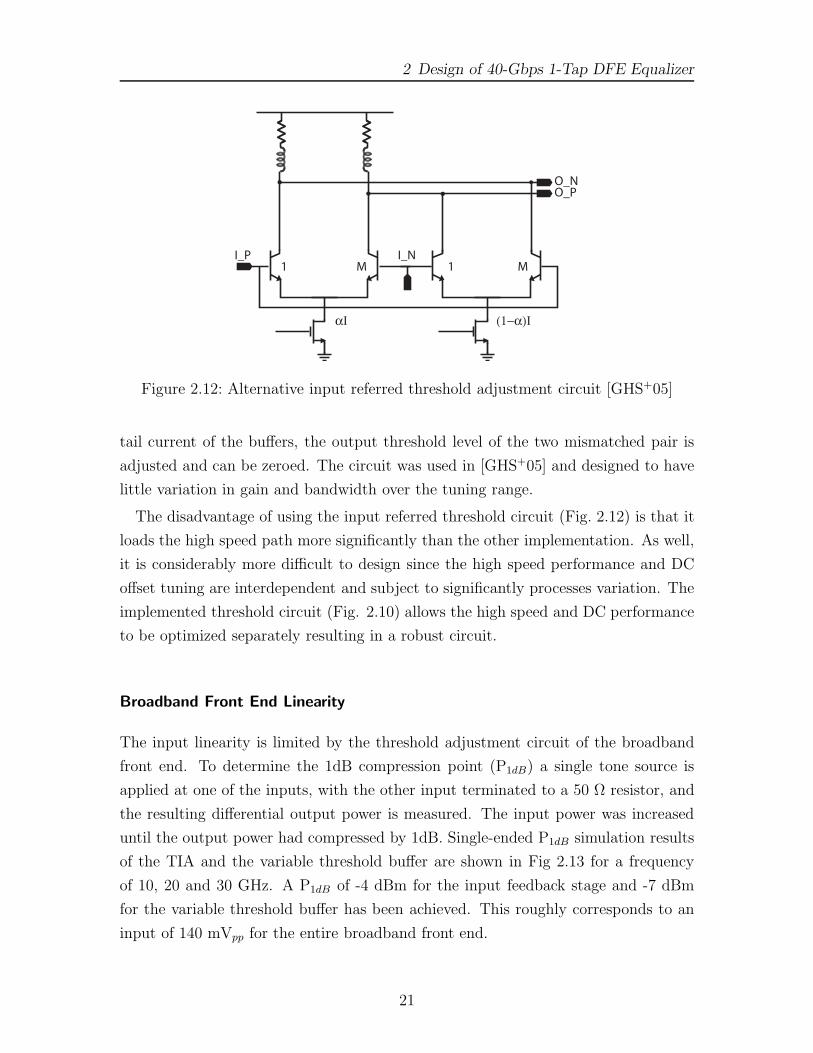
2 Design of 40-Gbps 1-Tap DFE Equalizer
I_P I_N
O_NO_P
M M
αI (1−α)I
1 1
Figure 2.12: Alternative input referred threshold adjustment circuit [GHS+05]
tail current of the buffers, the output threshold level of the two mismatched pair is
adjusted and can be zeroed. The circuit was used in [GHS+05] and designed to have
little variation in gain and bandwidth over the tuning range.
The disadvantage of using the input referred threshold circuit (Fig. 2.12) is that it
loads the high speed path more significantly than the other implementation. As well,
it is considerably more difficult to design since the high speed performance and DC
offset tuning are interdependent and subject to significantly processes variation. The
implemented threshold circuit (Fig. 2.10) allows the high speed and DC performance
to be optimized separately resulting in a robust circuit.
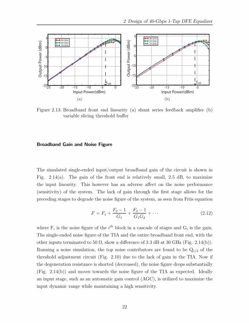
Broadband Front End Linearity
The input linearity is limited by the threshold adjustment circuit of the broadband
front end. To determine the 1dB compression point (P1dB) a single tone source is
applied at one of the inputs, with the other input terminated to a 50 Ω resistor, and
the resulting differential output power is measured. The input power was increased
until the output power had compressed by 1dB. Single-ended P1dB simulation results
of the TIA and the variable threshold buffer are shown in Fig 2.13 for a frequency
of 10, 20 and 30 GHz. A P1dB of -4 dBm for the input feedback stage and -7 dBm
for the variable threshold buffer has been achieved. This roughly corresponds to an
input of 140 mVpp for the entire broadband front end.
21
2 Design of 40-Gbps 1-Tap DFE Equalizer
-25 -20 -15 -10 -5 0
Input Power(dBm)
-20
-15
-10
-5
0
5O
utp
ut
Po
wer
(dB
m) 30 GHz
20 GHz10 GHz
P1dB
(a)
-25 -20 -15 -10 -5Input Power(dBm)
-20
-15
-10
-5
0
5
Ou
tpu
t P
ow
er (d
Bm
) 30 GHz20 GHz10 GHz
P1dB
(b)
Figure 2.13: Broadband front end linearity (a) shunt series feedback amplifier (b)variable slicing threshold buffer
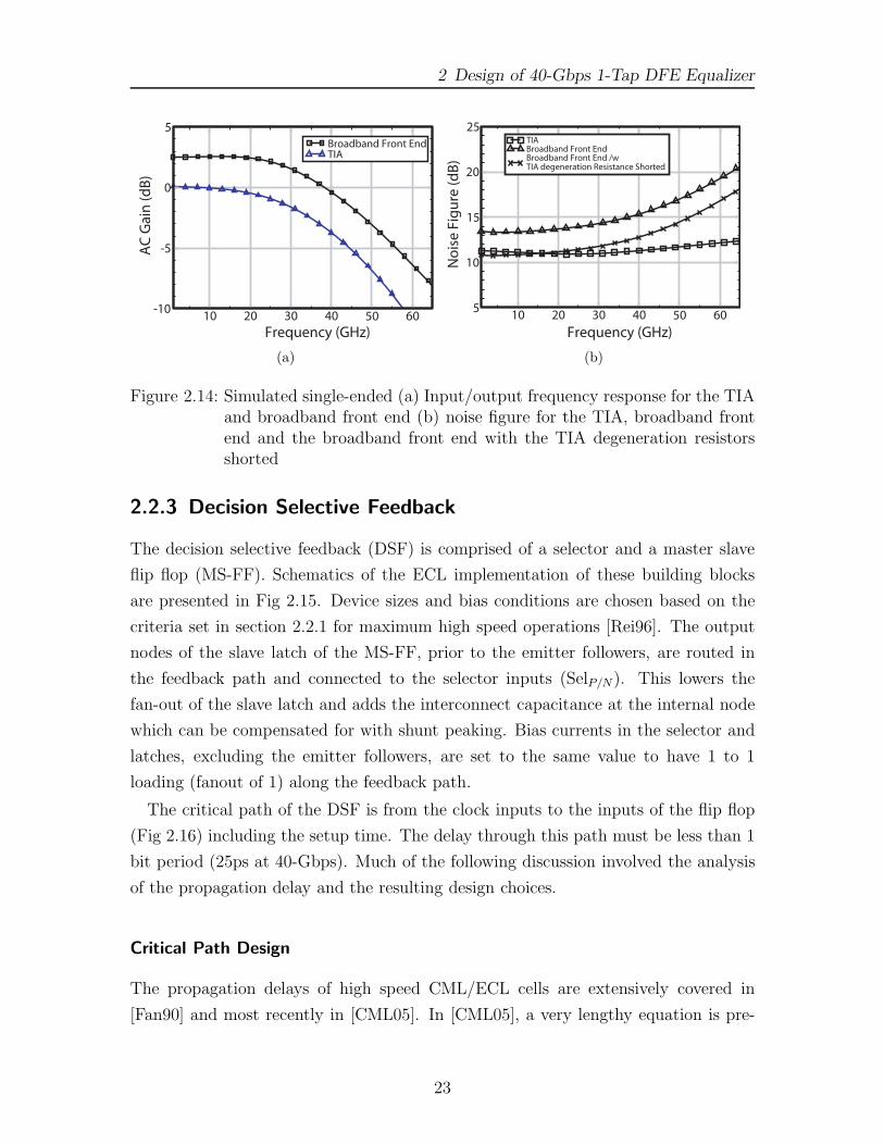
Broadband Gain and Noise Figure
The simulated single-ended input/output broadband gain of the circuit is shown in
Fig. 2.14(a). The gain of the front end is relatively small, 2.5 dB, to maximize
the input linearity. This however has an adverse affect on the noise performance
(sensitivity) of the system. The lack of gain through the first stage allows for the
preceding stages to degrade the noise figure of the system, as seen from Friis equation
F = F1 +F2 − 1
G1+
F3 − 1
G1G2+ · · · (2.12)
where Fi is the noise figure of the ith block in a cascade of stages and Gi is the gain.
The single-ended noise figure of the TIA and the entire broadband front end, with the
other inputs terminated to 50 Ω, show a difference of 3.3 dB at 30 GHz (Fig. 2.14(b)).
Running a noise simulation, the top noise contributors are found to be Q1/2 of the
threshold adjustment circuit (Fig. 2.10) due to the lack of gain in the TIA. Now if
the degeneration resistance is shorted (decreased), the noise figure drops substantially
(Fig. 2.14(b)) and moves towards the noise figure of the TIA as expected. Ideally
an input stage, such as an automatic gain control (AGC), is utilized to maximize the
input dynamic range while maintaining a high sensitivity.
22
2 Design of 40-Gbps 1-Tap DFE Equalizer
10 20 30 40 50 60Frequency (GHz)
-10
-5
0
5
AC
Gai
n (d
B)
Broadband Front EndTIA
(a)
10 20 30 40 50 60
Frequency (GHz)
5
10
15
20
25
No
ise
Fig
ure
(dB
)
TIABroadband Front EndBroadband Front End /w TIA degeneration Resistance Shorted
(b)
Figure 2.14: Simulated single-ended (a) Input/output frequency response for the TIAand broadband front end (b) noise figure for the TIA, broadband frontend and the broadband front end with the TIA degeneration resistorsshorted
2.2.3 Decision Selective Feedback
The decision selective feedback (DSF) is comprised of a selector and a master slave
flip flop (MS-FF). Schematics of the ECL implementation of these building blocks
are presented in Fig 2.15. Device sizes and bias conditions are chosen based on the
criteria set in section 2.2.1 for maximum high speed operations [Rei96]. The output
nodes of the slave latch of the MS-FF, prior to the emitter followers, are routed in
the feedback path and connected to the selector inputs (SelP/N). This lowers the
fan-out of the slave latch and adds the interconnect capacitance at the internal node
which can be compensated for with shunt peaking. Bias currents in the selector and
latches, excluding the emitter followers, are set to the same value to have 1 to 1
loading (fanout of 1) along the feedback path.
The critical path of the DSF is from the clock inputs to the inputs of the flip flop
(Fig 2.16) including the setup time. The delay through this path must be less than 1
bit period (25ps at 40-Gbps). Much of the following discussion involved the analysis
of the propagation delay and the resulting design choices.
Critical Path Design
The propagation delays of high speed CML/ECL cells are extensively covered in
[Fan90] and most recently in [CML05]. In [CML05], a very lengthy equation is pre-
23
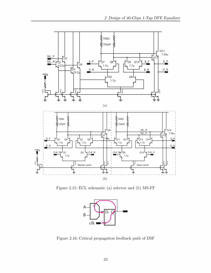
2 Design of 40-Gbps 1-Tap DFE Equalizer
D_P
D_N
100Ω
105pH
3mA
SEL_P
SEL_N
3mA
A_N
A_P
B_N
B_P
Q12 7.34μ
2mA
4mA
4.52μ
10.2μ
Q1
Q2
Q3
Q4Q7 1.7μ
Q8 Q9 1.7μ
Q10
Q5 1.7μ
Q6
1mA
Vdig
Q11
(a)
Q_P
Q_N
100Ω
135pH
3mA
CLK_N CLK_P
3mA
3mA
Q3 1.7μ
Q4 Q5 1.7μ
Q6 Q11 1.7μ
Q12 Q13 1.7μ
Q14
Q1 1.7μ
Q2 Q9 1.7μ
Q10
Q7 7.34μ
Q8
Q15
Q16 7.34μSEL_P
SEL_N
100Ω
105pH
3mA
CLK_P CLK_N
3mA
3mA
D_N
D_P
1mA
Vdig
Master Latch Slave Latch
(b)
Figure 2.15: ECL schematic (a) selector and (b) MS-FF
D Qs
clk
A
B
Figure 2.16: Critical propagation feedback path of DSF
24
2 Design of 40-Gbps 1-Tap DFE Equalizer
sented to represent the propagation delay through a bipolar flip flop. The equation
itself, however provides little intuition into the design of the feedback path of interest.
In [DBV05] the propagation delay of an HBT cascode pair is simplified to the major
contributors and is presented in equation 2.13. Even though the equation is not exact,
it does provide design insight. From equation 2.13 there are three general contribu-
tors to the propagation delay of an HBT cascode: the transistor time constants, the
parasitic interconnect capacitance, and the load resistance.
τpd ≈ ΔV (Cμ + Ccs + Cint)
It
+(k+Rb
Rl
)Rl(Cπ +(1 − Av) Cμ)+Cπ + Ccs + Cμ
gm
(2.13)
where
ΔV is the voltage swing of the ECL block
It is the tail current of the ECL block
Rl is the load resistance, Rl = ΔVIc
Rb is the base resistance of the transistor
Cμ is the base-collector capacitance of the transistor
Cπ is the base-emitter capacitance of the transistor
Ccs is the collector-substrate capacitance of the transistor
Cint is the interconnect capacitance
gm is the transconductance of the transistor
k is the stage-to-stage size scaling factor (fanout), 1 for this feedback path
Av is the gain of the input transistor of the cascode, approximately -1
The transistor time constants are determined by the transistor parasitic capacitance
(Cμ, Cπ, Ccs) and resistances (Rb, 1/gm). These terms also appear in the ft and fmax
equations and can be minimized by biasing at a collector current density of Jpeakft
[TN98].
Since the transistor time constants are strongly dependant on the collector current
density, and weakly on the collector current, low bias currents could be used to
minimize the power consumption. However, at low collector currents, the interconnect
capacitance (Cint) dominates the propagation time. Therefore, in order to minimize
this effect, the interconnect capacitance should be decreased and a collector current
should be selected which is power efficient, yet minimizes the propagation dependence
on Cint.
Lastly, the load resistance can be decreased for the same tail current (i.e. an ef-
25
2 Design of 40-Gbps 1-Tap DFE Equalizer
fective decrease in the voltage swing, ΔV ) to minimize the propagation time. There
is a limit to how small the voltage swing can be made while still providing function-
ality. From [CML05], the minimum voltage swing required to switch the following
differential pair is
ΔV ≥ 6Vt + IcRe (2.14)
where Vt = kT/q and Re is the emitter resistance. For negligible emitter resistances,
this is a swing of 150mV at room temperature. For noise immunity reasons the voltage
swing is often kept larger than this minimum value.
Using the general design guidelines, the ECL is biased near Jpeakft, with a tail
current of 3 mA, the interconnect capacitance is minimized by routing the feedback
path using the highest metal available and the output logic swing is set to approx-
imately 300 mV to provide enough noise margin for the following ECL stages. The
use of inductors also decreases the propagation delay [Lee98]. From simulations, a
propagation delay through the critical path is 21 ps without including the feedback
interconnect. Using ASITIC, the feedback interconnect is modeled and found to have
a distributed total inductance of 150 pH and capacitance of 15 fF. The interconnect
model increases the propagation delay to 22 ps. If the timing requirements had not
been sufficient, the voltage swing could have been decreased further. Other enhance-
ments, such as a keep-alive current [CML05], are also available, however they are
considerably more complicated.
2.2.4 Slicers
The slicer is comprised of 3 cascaded ECL buffers shown in Fig 2.17. A single buffer
could not be used since it would not provide the required gain while maintaining the
system bandwidth. Emitter degeneration of the differential pair (Q1/2,7/8,11/12) was
used to reduce the small signal gain of each of the buffers and to distribute it between
the 3 stages. A simulated gain of 5.5 dB per stage is achieved with an aggregated
small signal bandwidth of 27 GHz, which is adequate for a 40-Gbps system.
Buffer 1 and 3 of the slicer use differential cascode amplifiers to lower the Miller
effect on the input transistor (Q1/2,7/8,11/12). A cascode amplifier was not employed
for the second buffer since a lower common-mode voltage at the emitter of Q5,6 would
be required so that the cascode transistor would not saturate. In order to achieve
the CM shift two methods were investigated and ultimately discarded. Cascaded
emitter followers could have provided the correct CM level for the second buffer,
26
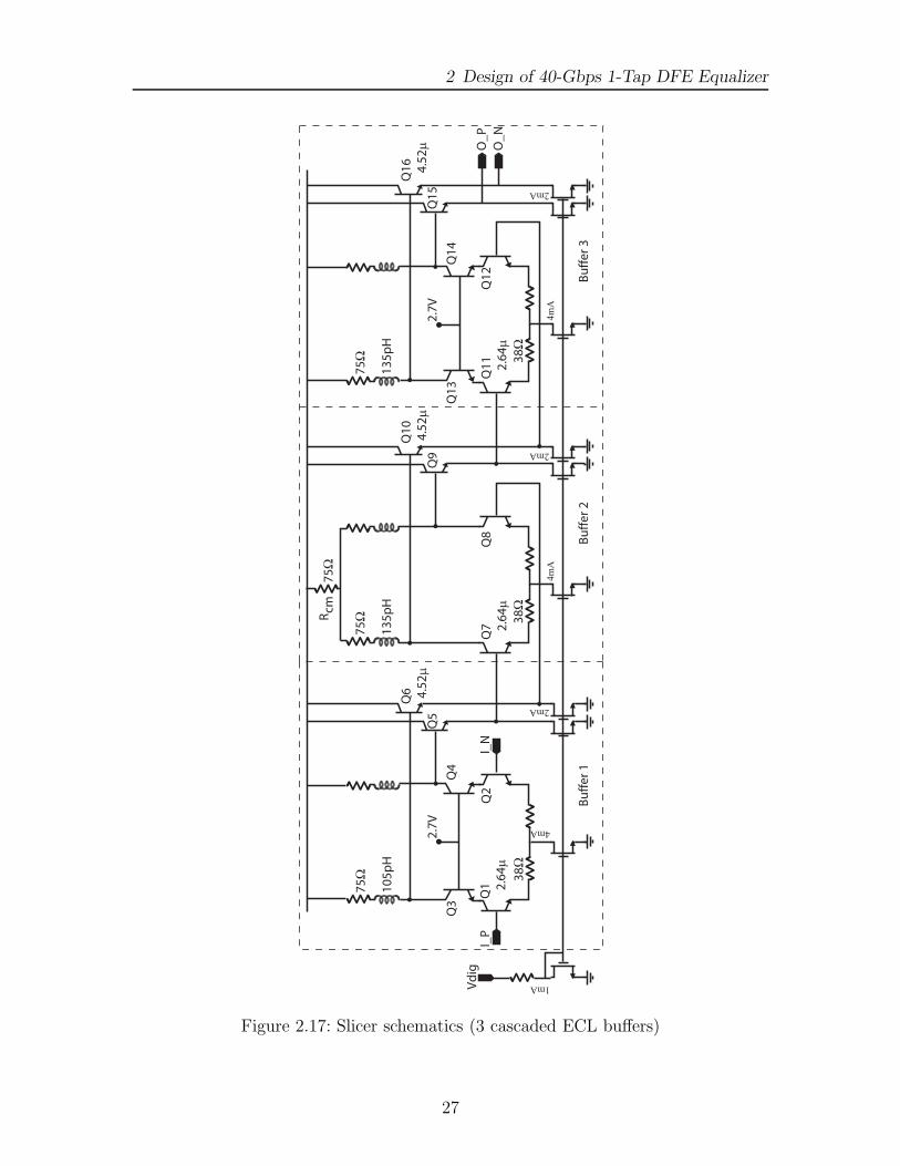
2 Design of 40-Gbps 1-Tap DFE Equalizer
O_P
O_N
75Ω
105p
H
38Ω
4mA
I_P
I_N
75Ω
135p
H
38Ω
75Ω
135p
H
38Ω
75Ω
4mA
4mA
Q1
2.
64μ
Q2
Q7
2.
64μ
Q8
Q11
2.
64μ
Q12
Q3
Q4
Q13
Q14
Q5
Q6
4.5
2μQ
9
Q10
4.5
2μQ
15
Q16
4.
52μ
2mA
2mA
2mA
1mAVd
ig
Rcm
Bu
ffer
1B
uff
er 2
Bu
ffer
3
2.7V
2.7V
Figure 2.17: Slicer schematics (3 cascaded ECL buffers)
27
2 Design of 40-Gbps 1-Tap DFE Equalizer
as well as increased the overall bandwidth of the slicers. The frequency response
of multiple emitter followers however has the potential to be underdamped due to
parasitic line inductance or the negative input impedance of the EF stages causing
significant “ringing” in the large signal response [Rei96]. Another method would
employ a diode connected transistor at the output of the emitter follower (Q5,6) to
provide the CM shift. The additional capacitance of the diode transistor decreases
the bandwidth of the slicer more significantly than the advantages of the cascode
amplifier. Since a bandwidth efficient CM level shit was not available a cascode
amplifier was not used in the second stage. The common-mode resistor (Rcm) in the
second buffer does however provide a DC shift to lower the common-mode voltage
into the third buffer allowing a cascode amplifier to be used.
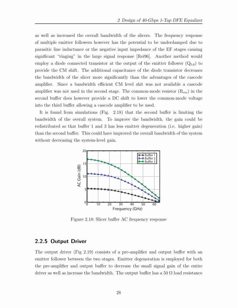
It is found from simulations (Fig. 2.18) that the second buffer is limiting the
bandwidth of the overall system. To improve the bandwidth, the gain could be
redistributed so that buffer 1 and 3 has less emitter degeneration (i.e. higher gain)
than the second buffer. This could have improved the overall bandwidth of the system
without decreasing the system-level gain.
0 10 20 30 40 50 60Frequency (GHz)
0
5
10
15
20
AC
Gai
n (d
B)
Buffer 1Buffer 2Buffer 3
Figure 2.18: Slicer buffer AC frequency response
2.2.5 Output Driver
The output driver (Fig 2.19) consists of a pre-amplifier and output buffer with an
emitter follower between the two stages. Emitter degeneration is employed for both
the pre-amplifier and output buffer to decrease the small signal gain of the entire
driver as well as increase the bandwidth. The output buffer has a 50 Ω load resistance
28
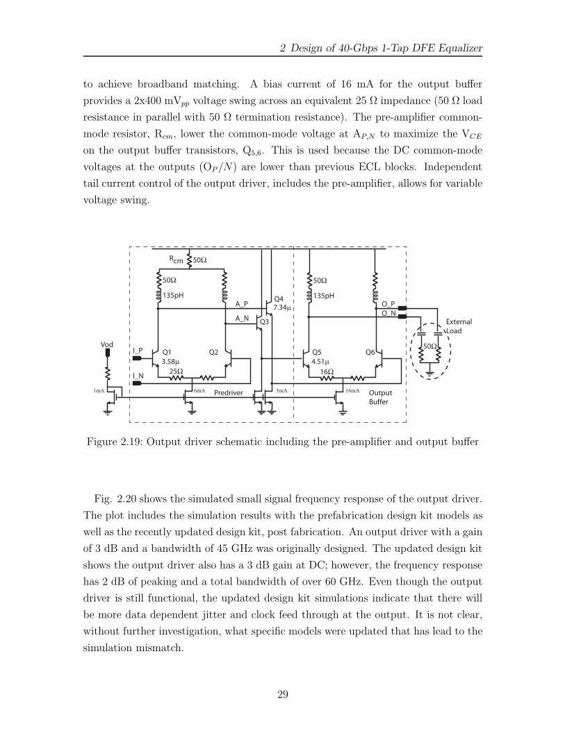
2 Design of 40-Gbps 1-Tap DFE Equalizer
to achieve broadband matching. A bias current of 16 mA for the output buffer
provides a 2x400 mVpp voltage swing across an equivalent 25 Ω impedance (50 Ω load
resistance in parallel with 50 Ω termination resistance). The pre-amplifier common-
mode resistor, Rcm, lower the common-mode voltage at AP,N to maximize the VCE
on the output buffer transistors, Q5,6. This is used because the DC common-mode
voltages at the outputs (OP /N) are lower than previous ECL blocks. Independent
tail current control of the output driver, includes the pre-amplifier, allows for variable
voltage swing.
50Ω
135pH
16Ω
50Ω
135pH
25Ω
50Ω
6mA 16mA3mA
O_NO_P
I_P
I_N
4.51μ Q5
3.58μ Q1 Q2 Q6
Q3
Q47.34μ
1mA
Vod
Rcm
A_N
A_P
Predriver OutputBuffer
ExternalLoad
50Ω
Figure 2.19: Output driver schematic including the pre-amplifier and output buffer
Fig. 2.20 shows the simulated small signal frequency response of the output driver.
The plot includes the simulation results with the prefabrication design kit models as
well as the recently updated design kit, post fabrication. An output driver with a gain
of 3 dB and a bandwidth of 45 GHz was originally designed. The updated design kit
shows the output driver also has a 3 dB gain at DC; however, the frequency response
has 2 dB of peaking and a total bandwidth of over 60 GHz. Even though the output
driver is still functional, the updated design kit simulations indicate that there will
be more data dependent jitter and clock feed through at the output. It is not clear,
without further investigation, what specific models were updated that has lead to the
simulation mismatch.
29
2 Design of 40-Gbps 1-Tap DFE Equalizer
10 20 30 40 50 60Frequency (GHz)
-10
-5
0
5
AC
Gai
n (d
B)
Post fabrication design kitPrefabrication design kit
Figure 2.20: Simulated output driver AC frequency response using the prefabricationand post fabrication design kit
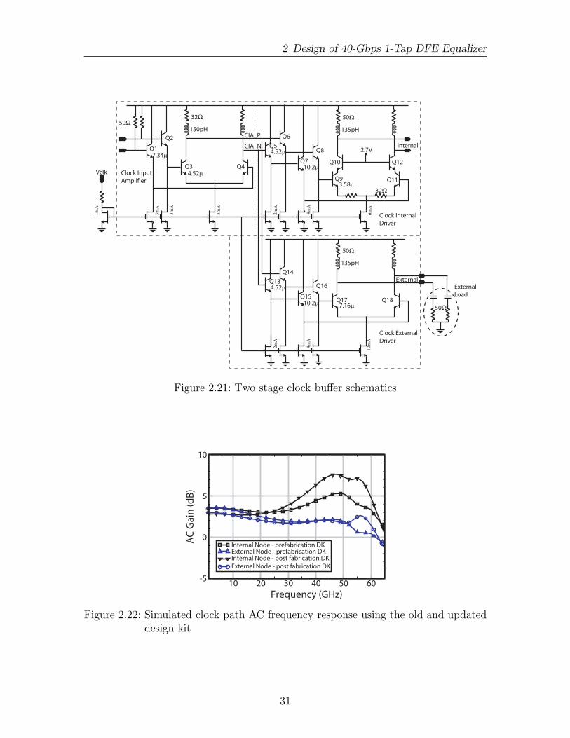
2.2.6 Clock Path
The clock distribution network can be seen in Fig. 2.21. The inputs into the emitter
followers (Q1,2) are matched with on-chip 50 Ω resistors to the power supply voltage.
Unlike the data path, which uses a TIA stage, a high sensitivity input amplifier is
not required. Cascaded emitter followers were used to increase the bandwidth of the
system since a bandwidth of at least 50 GHz was desired for the 40 GHz clock path.
The potential “ringing” caused by the double emitter follower is less of a concern,
as long as it is stable, give the clock signal is narrowband. The clock buffer has an
internal output that feeds the flip flop and an external output which is driven off
chip. It is intended that the external output could be used as a trigger signal for the
oscilloscope if high frequency splitters are not available during testing. The external
output has a voltage swing of 2x300mV.
Fig. 2.22 shows the simulated small signal frequency response of the clock buffer,
to the internal and external outputs, for both the prefabrication and post fabrication
design kit. A clock buffer with 3.5 dB gain and a bandwidth of 55 GHz to the
external outputs was designed. Similar to the output driver, the frequency response
of the clock path differ between the design kits.
2.3 Time-domain Simulations
Time-domain simulations were conducted to obtain the large signal performance of
the DFE. The input data stream is passed through a PMD channel with γ of 0.5 and
30
2 Design of 40-Gbps 1-Tap DFE Equalizer
50Ω150pH
8mA
3mA
32Ω
3mA
2mA
4mA
135pH
6mA
50Ω
2mA
4mA
32Ω3.58μ
4.52μ
7.34μ 4.52μ
10.2μ
4.52μ
10.2μ
Q1
Q2
Q3 Q4
Q9
Q5
Q6
Q7
Q8
Q13
Q14
Q15
Q16
Q11
Q12Q10
135pH
50Ω
7.16μQ17 Q18
12m
A
Internal
External
1mA
Vclk
2.7V
Clock InputAmplifier
Clock ExternalDriver
Clock InternalDriver
CIA_P
CIA_N
ExternalLoad
50Ω
Figure 2.21: Two stage clock buffer schematics
10 20 30 40 50 60Frequency (GHz)
-5
0
5
10
AC
Gai
n (d
B)
Internal Node - prefabrication DKExternal Node - prefabrication DKInternal Node - post fabrication DKExternal Node - post fabrication DK
Figure 2.22: Simulated clock path AC frequency response using the old and updateddesign kit
31
2 Design of 40-Gbps 1-Tap DFE Equalizer
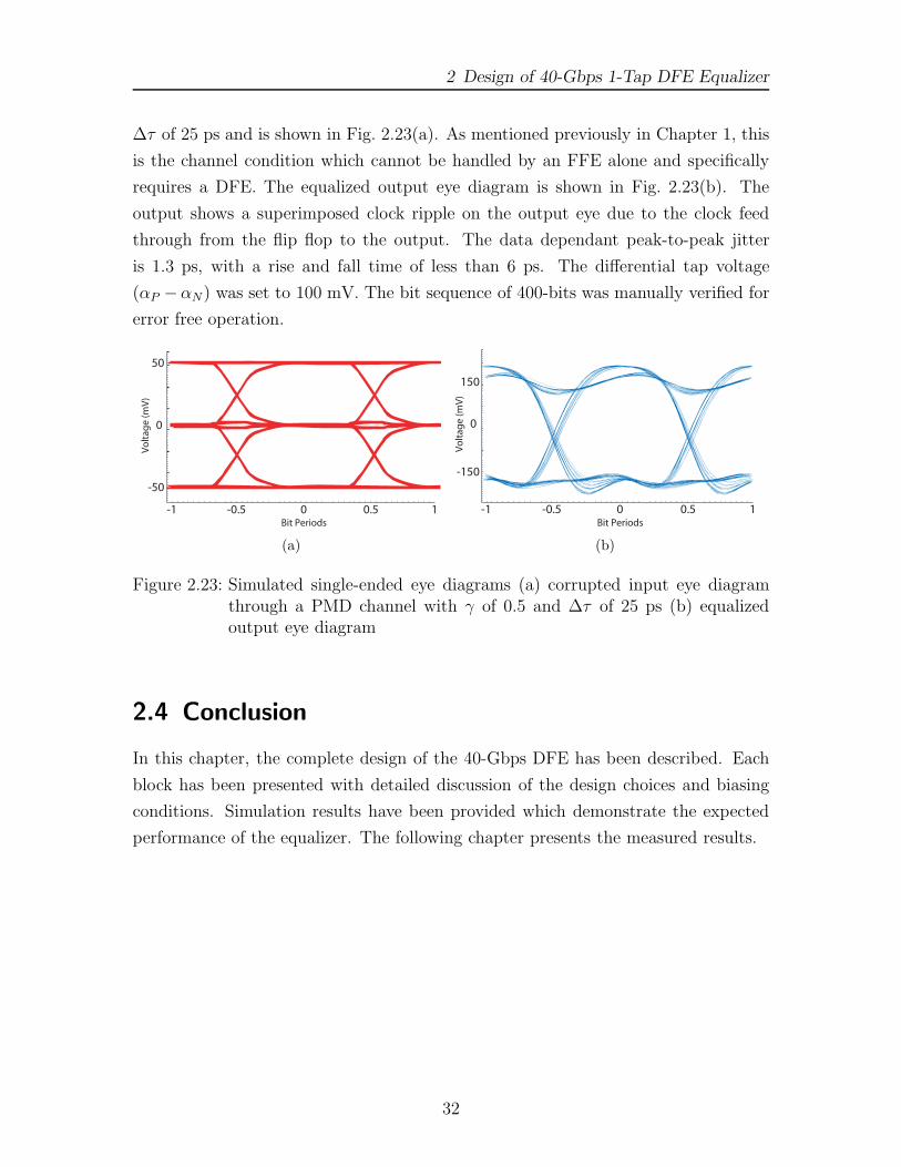
Δτ of 25 ps and is shown in Fig. 2.23(a). As mentioned previously in Chapter 1, this
is the channel condition which cannot be handled by an FFE alone and specifically
requires a DFE. The equalized output eye diagram is shown in Fig. 2.23(b). The
output shows a superimposed clock ripple on the output eye due to the clock feed
through from the flip flop to the output. The data dependant peak-to-peak jitter
is 1.3 ps, with a rise and fall time of less than 6 ps. The differential tap voltage
(αP −αN) was set to 100 mV. The bit sequence of 400-bits was manually verified for
error free operation.
-0.5Bit Periods
50
Vo
ltag
e (m
V)
0.50-1 1
-50
0
(a)
-0.5Bit Periods
150
Vo
ltag
e (m
V)
0.50-1 1
-150
0
(b)
Figure 2.23: Simulated single-ended eye diagrams (a) corrupted input eye diagramthrough a PMD channel with γ of 0.5 and Δτ of 25 ps (b) equalizedoutput eye diagram
2.4 Conclusion
In this chapter, the complete design of the 40-Gbps DFE has been described. Each
block has been presented with detailed discussion of the design choices and biasing
conditions. Simulation results have been provided which demonstrate the expected
performance of the equalizer. The following chapter presents the measured results.
32
3 Fabrication and Measurements
This chapter presents the measurements of the 40-Gbps DFE fabricated in Jazz Semi-
conductors’ SBC18HX 0.18μm SiGe BiCMOS technology with a 160-GHz ft [RK03].
Ideally, a 40-Gbps bit error tester (BERT) through a fiber optical channel, or PMD
emulator, would have been used to verify the functionality of the test chip; however,
in the absence of such system, a series of small signal and large signal tests were
completed. The aim of the following chapter is to characterize the DFE.
Section 3.1 presents the test chips fabricated based on the design in Chapter 2.
Section 3.2 summarizes the results of the S-parameter measurements including the
breakout front end bandwidth and return loss of the high speed ports of the DFE.
The P1dB of the front end breakout and the variable tap weight tuning are presented
in section 3.3. The bit error measurements at 5, 6 and 10 Gbps through a PMD emu-
lating board and 20-ft SMA cable are demonstrated in section 3.4. Lastly, section 3.5
outlines the measurement results at 35Gbps to 39.5Gbps including verification of the
correct bit sequence using an Agilent 86100C oscilloscope. All measurements were
performed on wafer.
3.1 Circuit Layout
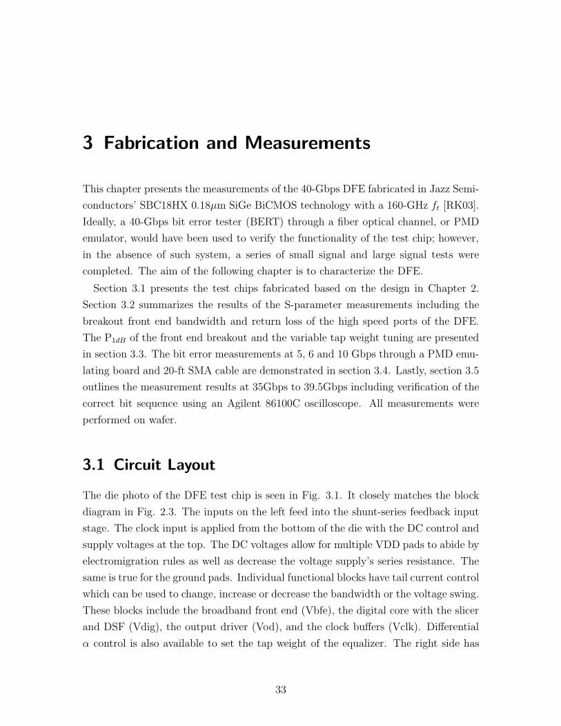
The die photo of the DFE test chip is seen in Fig. 3.1. It closely matches the block
diagram in Fig. 2.3. The inputs on the left feed into the shunt-series feedback input
stage. The clock input is applied from the bottom of the die with the DC control and
supply voltages at the top. The DC voltages allow for multiple VDD pads to abide by
electromigration rules as well as decrease the voltage supply’s series resistance. The
same is true for the ground pads. Individual functional blocks have tail current control
which can be used to change, increase or decrease the bandwidth or the voltage swing.
These blocks include the broadband front end (Vbfe), the digital core with the slicer
and DSF (Vdig), the output driver (Vod), and the clock buffers (Vclk). Differential
α control is also available to set the tap weight of the equalizer. The right side has
33
3 Fabrication and Measurements
1.5mm
1mmInputs
ClkInput
ClkOutput
Output
GN
D
VDD
Vbfe
GN
D
α_P
α_N
GN
D
VDD
Vdig
GN
D
Vod
Vclk
GN
D
VDD
Figure 3.1: DFE fabricated in Jazz Semiconductors’ SBC18HX 0.18μm SiGe BiCMOStechnology with a 160-GHz ft operating from a 3.3 V supply with 230 mAcurrent.
two sets of differential outputs for the clock and data. The IC occupies an area of
1.5 mm2 and operates from a 3.3 V power supply and draws 230 mA of current, of
which 60 mA is for the clock path.
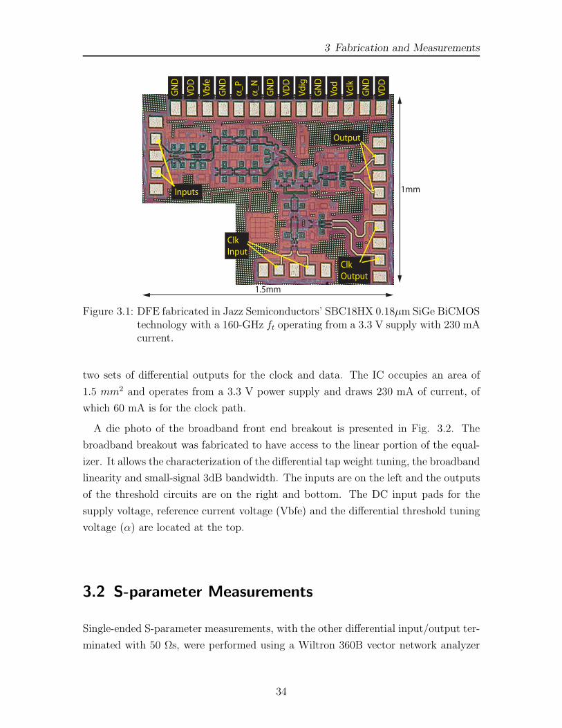
A die photo of the broadband front end breakout is presented in Fig. 3.2. The
broadband breakout was fabricated to have access to the linear portion of the equal-
izer. It allows the characterization of the differential tap weight tuning, the broadband
linearity and small-signal 3dB bandwidth. The inputs are on the left and the outputs
of the threshold circuits are on the right and bottom. The DC input pads for the
supply voltage, reference current voltage (Vbfe) and the differential threshold tuning
voltage (α) are located at the top.
3.2 S-parameter Measurements
Single-ended S-parameter measurements, with the other differential input/output ter-
minated with 50 Ωs, were performed using a Wiltron 360B vector network analyzer
34
3 Fabrication and Measurements
GN
D
VDD
Vbfe
GN
D
α_P
α_N
GN
D
Inputs
Output
Figure 3.2: Broadband front end fabricated in Jazz Semiconductors’ SBC18HX0.18μm SiGe BiCMOS technology with a 160-GHz ft operating from a3.3 V supply with 30 mA current.
(VNA), seen in Fig. 3.31. These small signal measurements are used to determine the
high speed performance of the DFE. Measurements show the single-ended return loss
(Fig 3.4(a)) of all the high speed ports for the DFE to be better than -10 dB up to
40 GHz. The bandwidth along the linear path from clock input to clock output (S43)
is shown in Fig. 3.4(c). A bandwidth greater than 50 GHz is achieved for the clock
distribution; however, there is excessive peaking near 40 GHz. This is attributed to
the use of cascaded emitter followers and the parasitic inductances within the layout.
With proper layout and design, the peaking can be minimized, which is observed by
lowering the bias current of the clock path, Fig. 3.4(d).
The VNA was also used to determine the 3dB bandwidth of the linear portions of
the data path. Single-ended S-parameter measurements of the front end breakout,
through the TIA and the top threshold adjustment circuit, with the other outputs
terminated, demonstrate a bandwidth of 45-GHz up to the slicers. The left-to-right
path is used to measure the bandwidth since calibration is considerably easier and
valid to a higher frequency. Given that the measurements are single-ended, the dif-
ferential gain is 6 dB higher than that presented in Fig. 3.4(b). The full data path
bandwidth could not be measured due to the nonlinear decision circuit.
3.3 Broadband Front End Breakout Characterization
The broadband front end breakout was tested to determine the systems equalization
performance. Following sections present the measured linearity and offset voltage
1It should be noted that the VNA does not perform 4-port measurements and Fig. 3.3 only providesreference port numbers for the data and clock inputs/outputs.
35
3 Fabrication and Measurements
67GHzProbe 67GHz
Probe
67GHzProbe
port 1 port 2
port 3
Vd
d (3
.3V;
230
mA
)
Vrf (
3.3V
; 1m
A)
Alp
haP
(1.8
V)
Vd
ig (3
.3V;
1m
A)
Alp
haN
(1.8
V)
Vod
rive
(3.3
V; 1
mA
)
Vcl
k (3
.3V;
1m
A)
DFE
DC BlockDC Block
DC
Blo
ck
67GHzProbe DC Block
port 4
Figure 3.3: S-Parameter measurement setup
tuning characteristics.
3.3.1 Linearity
The P1dB was measured to determine the linearity of the circuit over a wide range of
frequencies. A single signal source is applied to the input and the corresponding power
output is measured via a power meter (Fig. 3.5). To get accurate measurements, the
input and output cable/probe losses were de-embedded. Measurements at 1, 5, 10,
15, 20, and 30 GHz are presented in Fig. 3.6(a). A P1dB of -7.5dBm is achieved up
to 20 GHz (Fig. 3.6(b)).
The single-ended spectra of the output at the 1dB compression point for 5, 10,
and 20 GHz are seen in Fig. 3.7. Total harmonic distortion (THD) of the front end
breakout can be calculated using equation 3.1, where Pi is the power (W) in the ith
harmonic.
THD =P2 + P3 + · · ·+ Pi
P1∗ 100% (3.1)
The THD at the 1dB compression point is 0.62%, 1.09%, and 2% at 5, 10 and 20 GHz
respectively. If differential measurements were conducted, the actual THD would be
slightly lower since the second order harmonic would be suppressed significantly. The
third order harmonic of the 20 GHz signal was not seen since it was outside the
spectrum analyzer bandwidth and most likely the bandwidth of the breakout.
36
3 Fabrication and Measurements
10 20 30 40 50-30
-25
-20
-15
-10
-5
0S
11
S22
S33
Frequency (GHz)
S
(d
B)
Par
amet
er
0
(a)
10 20 30 40 50-20
-15
-10
-5
0
S
(d
B)
21
Frequency (GHz)0
SimulatedMeasured
(b)
10 20 30 40 50 60-10
-5
0
5
10
15
Frequency (GHz)
S
(dB
) 4
3
SimulatedMeasured
(c)
10 20 30 40 50 60-10
-5
0
5
10
15325uA550uA775uA1mA
Frequency (GHz)
S
(dB
) 4
3
(d)
Figure 3.4: S-Parameter (a) measured return loss for input, output and clock path, (b)measured and simulated broadband front end bandwidth, (c) measuredand simulated clock path frequency response and (d) measured clock pathfrequency response for various reference currents
Vd
d (3
.3V;
230
mA
)
Vrf (
3.3V
; 1m
A)
Alp
haP
(1.8
V)
Alp
haN
(1.8
V)
67GHzProbeDC Block
67GHzProbe DC Block
Agilent E8254DSignal Source
DC Block
P-seriesPower Meter
DC Block
Agilent E4448A PSA Spectrum Analyzer
Figure 3.5: P1dB measurement setup for the broadband front end breakout
37
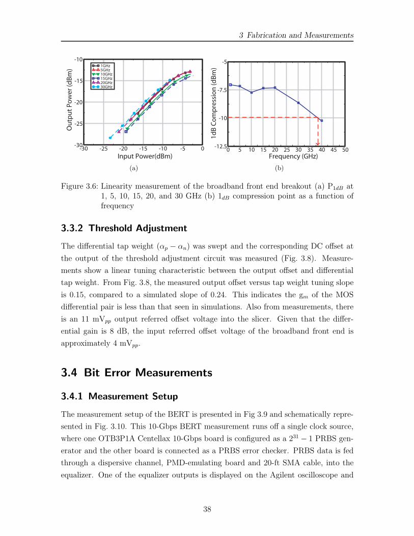
3 Fabrication and Measurements
-30 -25 -20 -15 -10 -5 0
Input Power(dBm)
-30
-25
-20
-15
-10
Ou
tpu
t P
ow
er (d
Bm
)1GHz5GHz10GHz15GHz20GHz30GHz
(a)
0 5 10 15 20 25 30 35 40 45 50Frequency (GHz)
-12.5
-10
-7.5
-5
1dB
Co
mp
ress
ion
(dB
m)
(b)
Figure 3.6: Linearity measurement of the broadband front end breakout (a) P1dB at1, 5, 10, 15, 20, and 30 GHz (b) 1dB compression point as a function offrequency
3.3.2 Threshold Adjustment
The differential tap weight (αp − αn) was swept and the corresponding DC offset at
the output of the threshold adjustment circuit was measured (Fig. 3.8). Measure-
ments show a linear tuning characteristic between the output offset and differential
tap weight. From Fig. 3.8, the measured output offset versus tap weight tuning slope
is 0.15, compared to a simulated slope of 0.24. This indicates the gm of the MOS
differential pair is less than that seen in simulations. Also from measurements, there
is an 11 mVpp output referred offset voltage into the slicer. Given that the differ-
ential gain is 8 dB, the input referred offset voltage of the broadband front end is
approximately 4 mVpp.
3.4 Bit Error Measurements
3.4.1 Measurement Setup
The measurement setup of the BERT is presented in Fig 3.9 and schematically repre-
sented in Fig. 3.10. This 10-Gbps BERT measurement runs off a single clock source,
where one OTB3P1A Centellax 10-Gbps board is configured as a 231 − 1 PRBS gen-
erator and the other board is connected as a PRBS error checker. PRBS data is fed
through a dispersive channel, PMD-emulating board and 20-ft SMA cable, into the
equalizer. One of the equalizer outputs is displayed on the Agilent oscilloscope and
38
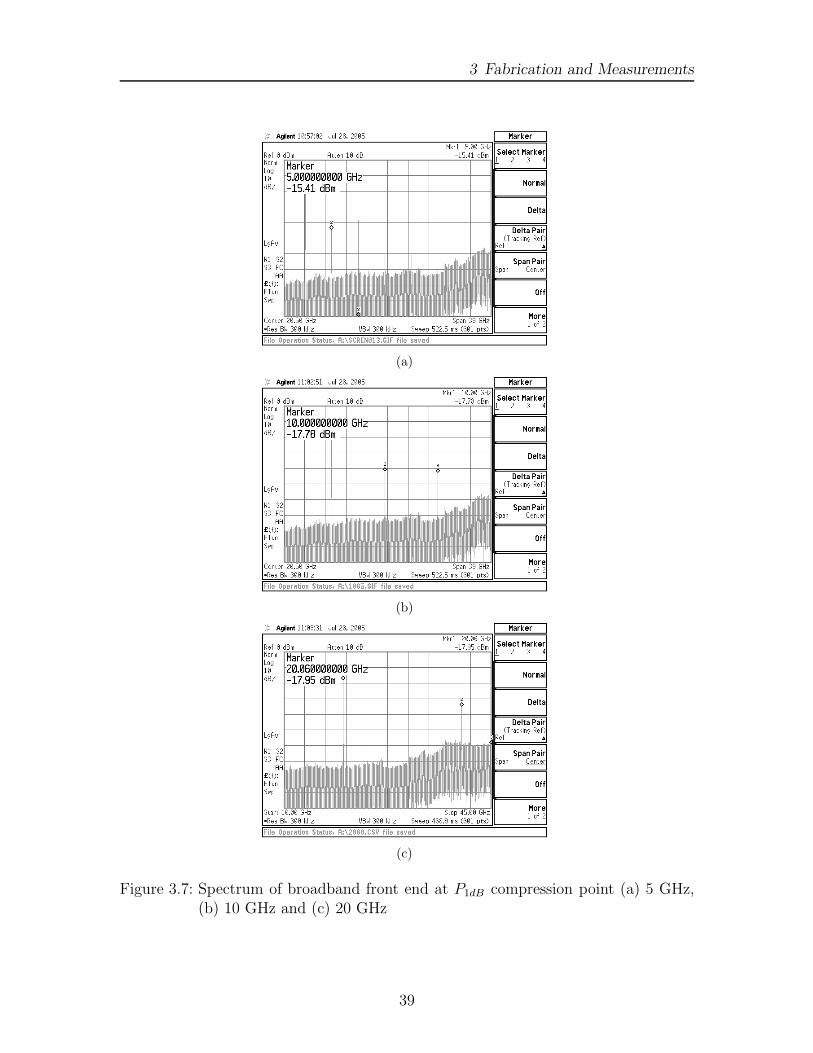
3 Fabrication and Measurements
(a)
(b)
(c)
Figure 3.7: Spectrum of broadband front end at P1dB compression point (a) 5 GHz,(b) 10 GHz and (c) 20 GHz
39
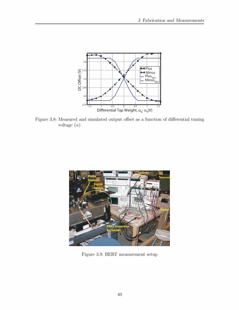
3 Fabrication and Measurements
-1.5 -1 -0.5 0 0.5 1 1.5
Differential Tap Weight, α - α (V)
2.35
2.4
2.45
2.5
2.55
2.6
DC
Off
set
(V) Plus
Minus
MinusSim
PlusSim
p n
Figure 3.8: Measured and simulated output offset as a function of differential tuningvoltage (α)
ProbeStation
DC Sources
SignalSource
Scope
Splitter
PRBS Generator& Checker
Figure 3.9: BERT measurement setup
40
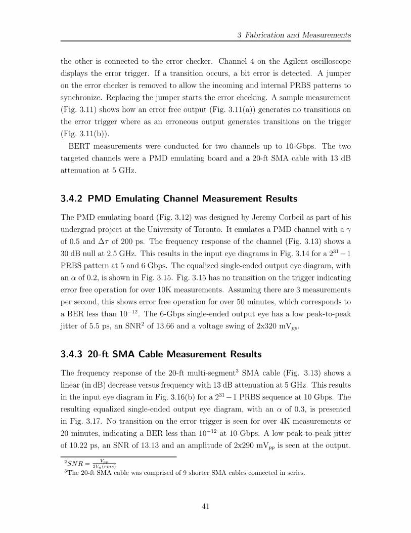
3 Fabrication and Measurements
the other is connected to the error checker. Channel 4 on the Agilent oscilloscope
displays the error trigger. If a transition occurs, a bit error is detected. A jumper
on the error checker is removed to allow the incoming and internal PRBS patterns to
synchronize. Replacing the jumper starts the error checking. A sample measurement
(Fig. 3.11) shows how an error free output (Fig. 3.11(a)) generates no transitions on
the error trigger where as an erroneous output generates transitions on the trigger
(Fig. 3.11(b)).
BERT measurements were conducted for two channels up to 10-Gbps. The two
targeted channels were a PMD emulating board and a 20-ft SMA cable with 13 dB
attenuation at 5 GHz.
3.4.2 PMD Emulating Channel Measurement Results
The PMD emulating board (Fig. 3.12) was designed by Jeremy Corbeil as part of his
undergrad project at the University of Toronto. It emulates a PMD channel with a γ
of 0.5 and Δτ of 200 ps. The frequency response of the channel (Fig. 3.13) shows a
30 dB null at 2.5 GHz. This results in the input eye diagrams in Fig. 3.14 for a 231−1
PRBS pattern at 5 and 6 Gbps. The equalized single-ended output eye diagram, with
an α of 0.2, is shown in Fig. 3.15. Fig. 3.15 has no transition on the trigger indicating
error free operation for over 10K measurements. Assuming there are 3 measurements
per second, this shows error free operation for over 50 minutes, which corresponds to
a BER less than 10−12. The 6-Gbps single-ended output eye has a low peak-to-peak
jitter of 5.5 ps, an SNR2 of 13.66 and a voltage swing of 2x320 mVpp.
3.4.3 20-ft SMA Cable Measurement Results
The frequency response of the 20-ft multi-segment3 SMA cable (Fig. 3.13) shows a
linear (in dB) decrease versus frequency with 13 dB attenuation at 5 GHz. This results
in the input eye diagram in Fig. 3.16(b) for a 231−1 PRBS sequence at 10 Gbps. The
resulting equalized single-ended output eye diagram, with an α of 0.3, is presented
in Fig. 3.17. No transition on the error trigger is seen for over 4K measurements or
20 minutes, indicating a BER less than 10−12 at 10-Gbps. A low peak-to-peak jitter
of 10.22 ps, an SNR of 13.13 and an amplitude of 2x290 mVpp is seen at the output.
2SNR = Vpp
2Vn(rms)3The 20-ft SMA cable was comprised of 9 shorter SMA cables connected in series.
41
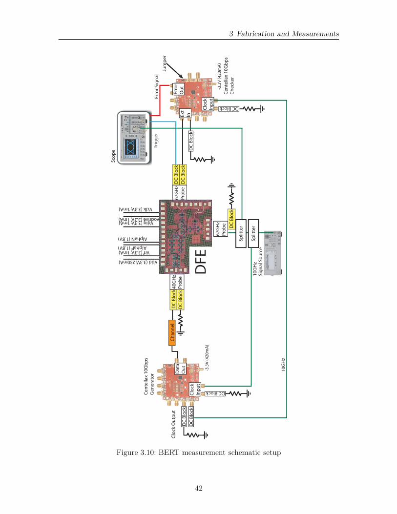
3 Fabrication and Measurements
-3.3
V (4
20m
A)
-3.3
V (4
20m
A)
DC
Blo
ck
DC
Blo
ck
DC
Blo
ck
40G
Hz
Pro
be
67G
Hz
Pro
be
67G
Hz
Pro
be
Sig
nal
So
urc
e
Cen
tella
x 10
Gb
ps
Gen
erat
or
Cen
tella
x 10
Gb
ps
Ch
ecke
r
Sco
pe
DC
Blo
ckD
C B
lock
DC
Blo
ck
10G
Hz
10G
Hz
Vdd (3.3V; 230mA)
Vrf (3.3V; 1mA)AlphaP (1.8V)
Vdig (3.3V; 1mA)
AlphaN (1.8V)
Vodrive (3.3V; 1mA)
Vclk (3.3V; 1mA)
DFE
Split
ter
DC
Blo
ck
DC Block
DC
Blo
ck
Jum
per
Erro
r Sig
nal
Trig
ger
Ch
ann
el
DC Block
Clo
ckIn
pu
tC
lock
Inp
ut
Dat
aO
ut
Ext
In
Erro
rO
ut
Split
ter
Clo
ck O
utp
ut
Figure 3.10: BERT measurement schematic setup
42
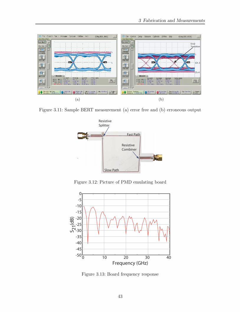
3 Fabrication and Measurements
(a)
Ch. 4
Ch. 3
ErrorTransition
(b)
Figure 3.11: Sample BERT measurement (a) error free and (b) erroneous output
ResistiveSplitter
Fast Path
Slow Path
ResistiveCombiner
Figure 3.12: Picture of PMD emulating board
40
Frequency (GHz)
-50
-45
-40
-35
-30
-25
-20
-15
-10
-5
0
0 10 20 30
S (d
B)
21
Figure 3.13: Board frequency response
43
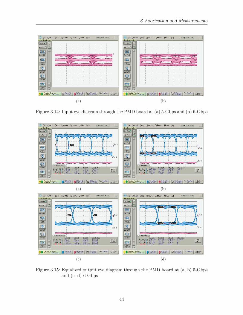
3 Fabrication and Measurements
(a) (b)
Figure 3.14: Input eye diagram through the PMD board at (a) 5-Gbps and (b) 6-Gbps
Ch. 4
Ch. 3
(a)
Ch. 4
Ch. 3
(b)
Ch. 4
Ch. 3
(c)
Ch. 4
Ch. 3
(d)
Figure 3.15: Equalized output eye diagram through the PMD board at (a, b) 5-Gbpsand (c, d) 6-Gbps
44
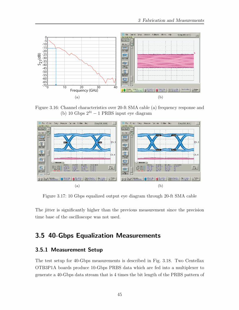
3 Fabrication and Measurements
-70-65-60-55-50-45-40-35-30-25-20-15-10
-50
S (d
B)
Frequency (GHz)0 40302010
21
(a) (b)
Figure 3.16: Channel characteristics over 20-ft SMA cable (a) frequency response and(b) 10 Gbps 231 − 1 PRBS input eye diagram
Ch. 4
Ch. 3
(a)
Ch. 4
Ch. 3
(b)
Figure 3.17: 10 Gbps equalized output eye diagram through 20-ft SMA cable
The jitter is significantly higher than the previous measurement since the precision
time base of the oscilloscope was not used.
3.5 40-Gbps Equalization Measurements
3.5.1 Measurement Setup
The test setup for 40-Gbps measurements is described in Fig. 3.18. Two Centellax
OTB3P1A boards produce 10-Gbps PRBS data which are fed into a multiplexer to
generate a 40-Gbps data stream that is 4 times the bit length of the PRBS pattern of
45
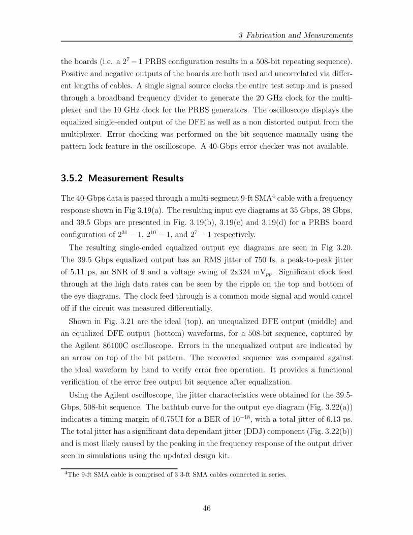
3 Fabrication and Measurements
the boards (i.e. a 27 −1 PRBS configuration results in a 508-bit repeating sequence).
Positive and negative outputs of the boards are both used and uncorrelated via differ-
ent lengths of cables. A single signal source clocks the entire test setup and is passed
through a broadband frequency divider to generate the 20 GHz clock for the multi-
plexer and the 10 GHz clock for the PRBS generators. The oscilloscope displays the
equalized single-ended output of the DFE as well as a non distorted output from the
multiplexer. Error checking was performed on the bit sequence manually using the
pattern lock feature in the oscilloscope. A 40-Gbps error checker was not available.
3.5.2 Measurement Results
The 40-Gbps data is passed through a multi-segment 9-ft SMA4 cable with a frequency
response shown in Fig 3.19(a). The resulting input eye diagrams at 35 Gbps, 38 Gbps,
and 39.5 Gbps are presented in Fig. 3.19(b), 3.19(c) and 3.19(d) for a PRBS board
configuration of 231 − 1, 210 − 1, and 27 − 1 respectively.
The resulting single-ended equalized output eye diagrams are seen in Fig 3.20.
The 39.5 Gbps equalized output has an RMS jitter of 750 fs, a peak-to-peak jitter
of 5.11 ps, an SNR of 9 and a voltage swing of 2x324 mVpp. Significant clock feed
through at the high data rates can be seen by the ripple on the top and bottom of
the eye diagrams. The clock feed through is a common mode signal and would cancel
off if the circuit was measured differentially.
Shown in Fig. 3.21 are the ideal (top), an unequalized DFE output (middle) and
an equalized DFE output (bottom) waveforms, for a 508-bit sequence, captured by
the Agilent 86100C oscilloscope. Errors in the unequalized output are indicated by
an arrow on top of the bit pattern. The recovered sequence was compared against
the ideal waveform by hand to verify error free operation. It provides a functional
verification of the error free output bit sequence after equalization.
Using the Agilent oscilloscope, the jitter characteristics were obtained for the 39.5-
Gbps, 508-bit sequence. The bathtub curve for the output eye diagram (Fig. 3.22(a))
indicates a timing margin of 0.75UI for a BER of 10−18, with a total jitter of 6.13 ps.
The total jitter has a significant data dependant jitter (DDJ) component (Fig. 3.22(b))
and is most likely caused by the peaking in the frequency response of the output driver
seen in simulations using the updated design kit.
4The 9-ft SMA cable is comprised of 3 3-ft SMA cables connected in series.
46
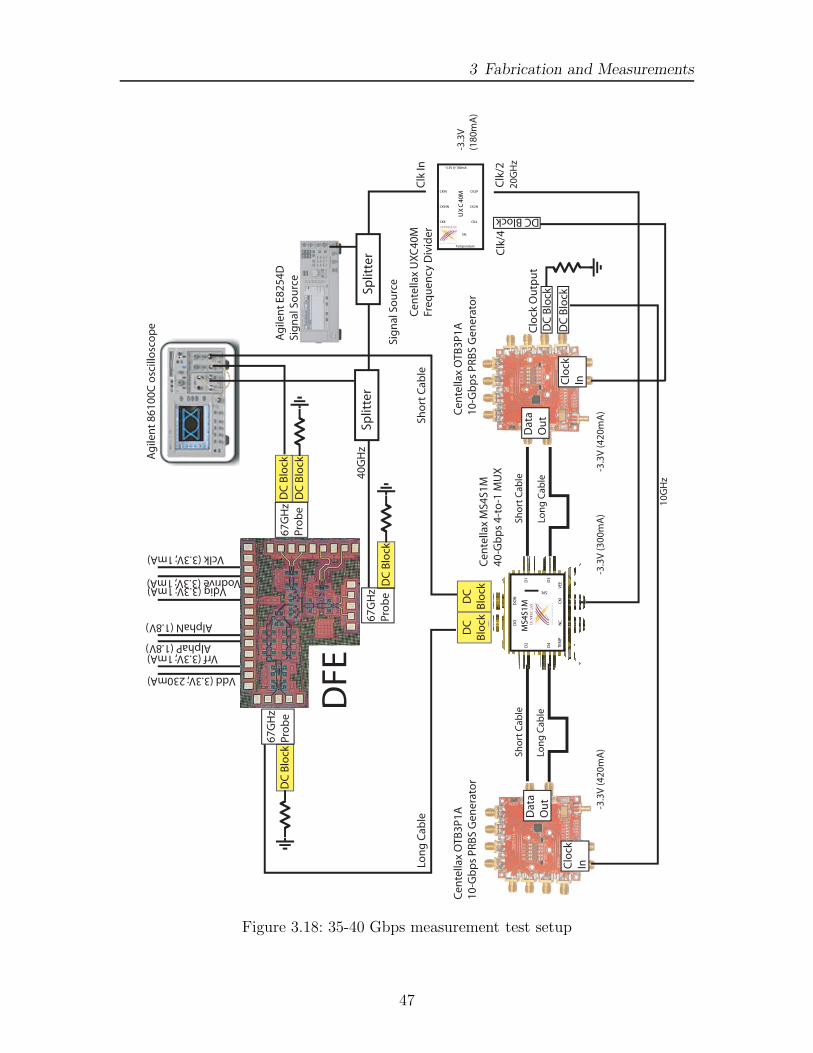
3 Fabrication and Measurements
-3.3
V (4
20m
A)
Cen
tella
x O
TB3P
1A
10-G
bp
s PR
BS
Gen
erat
or
Clo
ckIn
Dat
aO
ut
Sho
rt C
able
Lon
g C
able
-3.3
V (3
00m
A)
Sho
rt C
able
Lon
g C
able
20G
Hz
10G
Hz
DC
Blo
ckD
CB
lock
DC
Blo
ck
DC
Blo
ck
67G
Hz
Pro
be
67G
Hz
Pro
be
67G
Hz
Pro
be
Vdd (3.3V; 230mA)
Vrf (3.3V; 1mA)AlphaP (1.8V)
Vdig (3.3V; 1mA)
AlphaN (1.8V)
Vodrive (3.3V; 1mA)
Vclk (3.3V; 1mA)
40G
Hz
Split
ter
DC
Blo
ck
Ag
ilen
t E8
254D
Sig
nal
So
urc
e
Sig
nal
So
urc
e
Cen
tella
x M
S4S1
M40
-Gb
ps
4-to
-1 M
UX
Ag
ilen
t 86
100C
osc
illo
sco
pe
DC
Blo
ck
DFE
Lon
g C
able
Sho
rt C
able
-3.3
V (4
20m
A)C
ente
llax
OTB
3P1A
10
-Gb
ps
PRB
S G
ener
ato
r
DC
Blo
ck
DC
Blo
ckC
lock
Ou
tpu
t
Clo
ckIn
Dat
aO
ut
Split
ter
SN:
Temperature
−3.3V @ 180mA
M04C
XU
CK8 CK4
CK2N
CK2PCKIN
CKINN
Clk
In
Clk
/4C
lk/2
-3.3
V
(180
mA
)
: NS
D1
D3
D4
D2
NC
MS4
S1M C
KI
VEE
DO
DO
N
TEM
P
Cen
tella
x U
XC40
MFr
equ
ency
Div
ider
DC Block
Figure 3.18: 35-40 Gbps measurement test setup
47
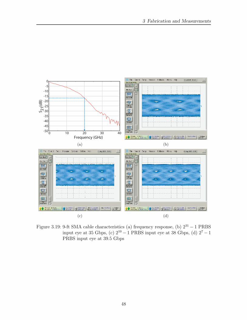
3 Fabrication and Measurements
Frequency (GHz)
-50
-45
-40
-35
-30
-25
-20
-15
-10
-5
0
400 10 20 30
S (d
B)
21
(a) (b)
(c) (d)
Figure 3.19: 9-ft SMA cable characteristics (a) frequency response, (b) 231 − 1 PRBSinput eye at 35 Gbps, (c) 210 − 1 PRBS input eye at 38 Gbps, (d) 27 − 1PRBS input eye at 39.5 Gbps
48
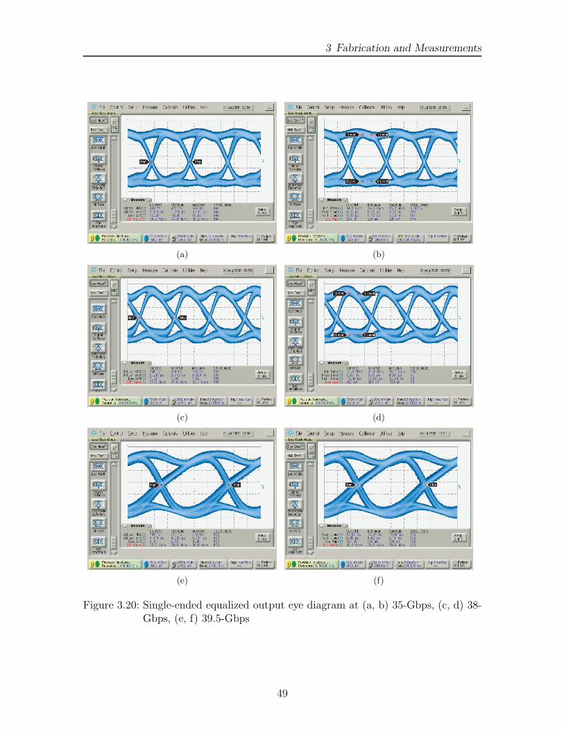
3 Fabrication and Measurements
(a) (b)
(c) (d)
(e) (f)
Figure 3.20: Single-ended equalized output eye diagram at (a, b) 35-Gbps, (c, d) 38-Gbps, (e, f) 39.5-Gbps
49
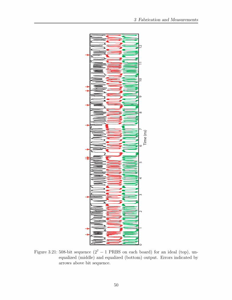
3 Fabrication and Measurements
01
23
49
1011
125
67
8
Tim
e (n
s)
Figure 3.21: 508-bit sequence (27 − 1 PRBS on each board) for an ideal (top), un-equalized (middle) and equalized (bottom) output. Errors indicated byarrows above bit sequence.
50
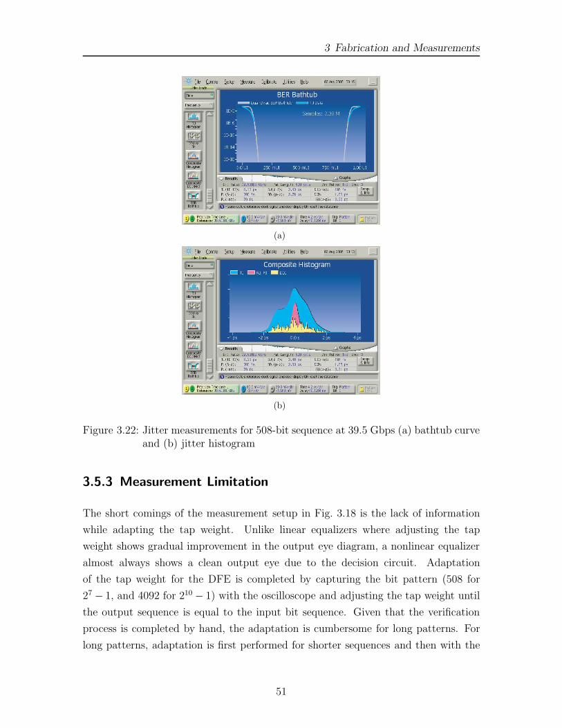
3 Fabrication and Measurements
(a)
(b)
Figure 3.22: Jitter measurements for 508-bit sequence at 39.5 Gbps (a) bathtub curveand (b) jitter histogram
3.5.3 Measurement Limitation
The short comings of the measurement setup in Fig. 3.18 is the lack of information
while adapting the tap weight. Unlike linear equalizers where adjusting the tap
weight shows gradual improvement in the output eye diagram, a nonlinear equalizer
almost always shows a clean output eye due to the decision circuit. Adaptation
of the tap weight for the DFE is completed by capturing the bit pattern (508 for
27 − 1, and 4092 for 210 − 1) with the oscilloscope and adjusting the tap weight until
the output sequence is equal to the input bit sequence. Given that the verification
process is completed by hand, the adaptation is cumbersome for long patterns. For
long patterns, adaptation is first performed for shorter sequences and then with the
51
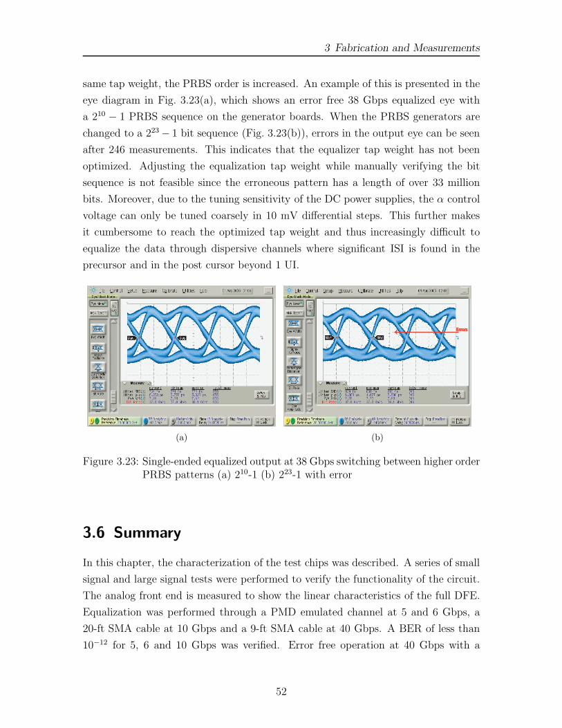
3 Fabrication and Measurements
same tap weight, the PRBS order is increased. An example of this is presented in the
eye diagram in Fig. 3.23(a), which shows an error free 38 Gbps equalized eye with
a 210 − 1 PRBS sequence on the generator boards. When the PRBS generators are
changed to a 223 − 1 bit sequence (Fig. 3.23(b)), errors in the output eye can be seen
after 246 measurements. This indicates that the equalizer tap weight has not been
optimized. Adjusting the equalization tap weight while manually verifying the bit
sequence is not feasible since the erroneous pattern has a length of over 33 million
bits. Moreover, due to the tuning sensitivity of the DC power supplies, the α control
voltage can only be tuned coarsely in 10 mV differential steps. This further makes
it cumbersome to reach the optimized tap weight and thus increasingly difficult to
equalize the data through dispersive channels where significant ISI is found in the
precursor and in the post cursor beyond 1 UI.
(a)
ErrorsErrors
(b)
Figure 3.23: Single-ended equalized output at 38 Gbps switching between higher orderPRBS patterns (a) 210-1 (b) 223-1 with error
3.6 Summary
In this chapter, the characterization of the test chips was described. A series of small
signal and large signal tests were performed to verify the functionality of the circuit.
The analog front end is measured to show the linear characteristics of the full DFE.
Equalization was performed through a PMD emulated channel at 5 and 6 Gbps, a
20-ft SMA cable at 10 Gbps and a 9-ft SMA cable at 40 Gbps. A BER of less than
10−12 for 5, 6 and 10 Gbps was verified. Error free operation at 40 Gbps with a
52
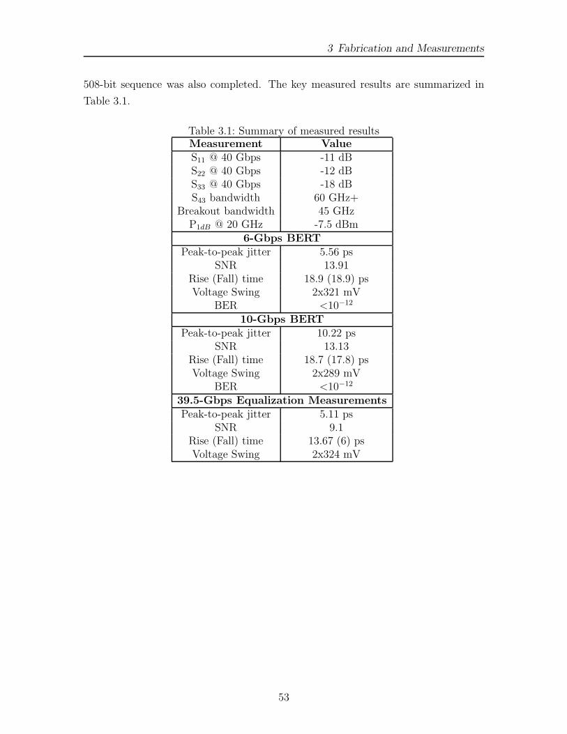
3 Fabrication and Measurements
508-bit sequence was also completed. The key measured results are summarized in
Table 3.1.
Table 3.1: Summary of measured resultsMeasurement ValueS11 @ 40 Gbps -11 dBS22 @ 40 Gbps -12 dBS33 @ 40 Gbps -18 dBS43 bandwidth 60 GHz+
Breakout bandwidth 45 GHzP1dB @ 20 GHz -7.5 dBm
6-Gbps BERTPeak-to-peak jitter 5.56 ps
SNR 13.91Rise (Fall) time 18.9 (18.9) psVoltage Swing 2x321 mV
BER <10−12
10-Gbps BERTPeak-to-peak jitter 10.22 ps
SNR 13.13Rise (Fall) time 18.7 (17.8) psVoltage Swing 2x289 mV
BER <10−12
39.5-Gbps Equalization MeasurementsPeak-to-peak jitter 5.11 ps
SNR 9.1Rise (Fall) time 13.67 (6) psVoltage Swing 2x324 mV
53
4 Conclusion and Future Work
The design of a 1-tap 40-Gbps decision feedback equalizer has been investigated for
PMD compensation of single-mode fibre. In order to meet the high speed require-
ments, a look-ahead architecture is selected to decrease the propagation delay within
the feedback path, while maintaining full functionality. Slight modifications to the
architecture were made to ease the requirements on the clock distribution and reduce
the overall power consumption of the DFE. A broadband front end provides a low
noise, linear input stage with a bandwidth of 45 GHz. The differential tap weight
was able to compensate for 225 mV of ISI using the threshold adjustment circuit. A
propagation delay of 22ps from simulations is found through the critical path when
interconnect parasitics are included. From measurements the DFE is shown to equal-
ize a PMD emulating channel at 5 and 6 Gbps as well as a 20-ft SMA cable at 10 Gbps
using a bit error checker. At 40 Gbps, the DFE compensated for a 9-ft SMA cable
and the functional verification was conducted by hand. All the inputs/outputs of the
DFE are suitable for high speed operation since they have a broadband matching of
better than -10dB up to 40 GHz. The test chip occupies an area of 1.5 mm2 and
operates from a 3.3 V power supply and draws 230 mA of current.
To the author’s knowledge, this is the first fully functional 40-Gbps DFE in any
technology. It has been shown that using current commercially available technologies,
equalizers at 40-Gbps are feasible [HV04] and previous assumptions on technology
limitations are no longer valid. This work sets the stage for larger equalizer systems
suitable for 40-Gbps fibre systems. With proper high speed design fully functional
equalizers can be created.
Future work can involve the integration of an FFE with this DFE to create a
complete PMD compensation system. As well, implementation of an AGC with a
high dynamic range, bandwidth and sensitivity at 40 Gbps is still required. Moreover
system level issues with an equalizer still exist. An adaptive algorithm for setting the
tap weights has been accomplished at 10 Gbps and must be investigated for adoption
at 40 Gbps. As well, low power clock recovery for the look-ahead architecture poses
significant issues. The full implementation of a multiple tap FFE-DFE equalizer with
54

4 Conclusion and Future Work
clock recovery and adaptive algorithms is a staggeringly vast task and area of research
yet to be fully explored.
This work is a first step at solving current impairments of fibre optical systems. It
is only a matter of time before OC-768 systems will be in place to meet the growing
bandwidth needs.
55
References
[BB04] Fred Buchali and Henning Bulow. Adaptive PMD Compensation byElectrical and Optical Techniques. IEEE/OSA Journal of LightwaveTechnology, 22(4):1116–1126, April 2004.
[BBB+00] H. Bulow, F. Buchali, W. Baumert, R. Ballentin, and T. Wehren. PMDmitigation at 10Gb/s using linear and nonlinear integrated electronicequalizer circuits. Electronics Letters, 36(2):163–164, 2000.
[CML05] Thomas E. Collins, Vikas Manan, and Stephen I. Long. Design analy-sis and circuit enhancements for high-speed bipolar flip-flops. IEEEJournal of Solid-State Circuits, 40(5):1166–1174, May 2005.
[DBV05] Timothy O. Dickson, Rudy Beerkens, and Sorin P. Voinigescu. A 2.5-V45-Gb/s Decision Circuit using SiGe BiCMOS Logic. IEEE Journal ofSolid-State Circuits, 40(4):994–1003, April 2005.
[DLB+05] Timothy O. Dickson, Marc-Andre LaCroix, Samuel Boret, Daniel Glo-ria, Rudy Beerkens, and Sorin P. Voinigescu. 30-100 GHz Inductorsand Transformers for Millimeter-wave (Bi)CMOS Integrated Circuits.IEEE Transactions on Microwave Theory and Techniques, 53(1):123–133, January 2005.
[Fan90] Wen Fang. Accurate Analytical Delay Expressions for ECL and CMLCircuits and their applications to optimizing high-speed bipolar cir-cuits. IEEE Journal of Solid-State Circuits, 25(2):572–583, April 1990.
[GHS+05] Bruno Garlepp, Andrew Ho, Vladimir Stojanovic, Fred Chen, CarlWerner, Grace Tsang, Tim Thrush, Amita Agarwal, and Jared Zerbe.A 1-10Gbps PAM2, PAM4, PAM2 Partial Response Receiver AnalogFront End with Dynamic Sampler Swapping Capability for BackplaneSerial Communications. In Digest of Papers IEEE VLSI Symposium,pages 376–379, June 2005.
[HPM+03] H.Tran, F. Pera, D. S. McPherson, D. Viorel, and S. P. Voinigescu.6kΩ, 43 Gb/s differential transimpedance-limiting amplifier with auto-zero feedback and high dynamic range. IEEE GaAs IC Symp. Tech.Dig., pages 241–244, 2003.
56
4 References
[HV04] Altan Hazneci and Sorin P. Voinigescu. A 49-Gb/s, 7-Tap TransversalFilter in 0.18μm SiGe BiCMOS for Backplane equalization. In IEEECSIC Digest, pages 101–104, Oct 2004.
[JM97] David A. Johns and Ken Martin. Analog Integrated Circuit Design.John Wiley & Sons, Hobokan, New Jersey, 1997.
[KBPC+05] Nagendra Krishnapura, Majid Barazande-Pour, Qasim Chaudhry, JohnKhoury, Kadaba Lakshmikumar, and Akshay Aggarwal. A 5Gb/s NRZTransceiver with Adaptive Equalization for Backplane Transmission. InProc. IEEE International Solid-State Circuits Conference, number 3.1,pages 60–61, Feb 2005.
[KHB97] Ravinder S. Kajley, Paul J. Hurst, and James E. C. Brown. A Mixed-Signal Decision-Feedback Equalizer that uses a look-ahead architecture.IEEE Journal of Solid-State Circuits, 32(3):450–459, March 1997.
[KW91] Sanjay Kasturia and Jack H. Winters. Techniques for high-speed imple-mentation of nonlinear cancellation. IEEE Journal on Selected Areasin Communications, 9(5):711–717, June 1991.
[KYMW+05] Kannan Krishna, David A. Yokoyama-Martin, Skye Wolfer, ChrisJones, Mat Loikkanen, James Parker, Ross Segelken, Jeff L. Sonntag,John Stonick, Steve Titus, and Daniel Weinlader. A 0.6 to 9.6Gb/sBinary Backplane Transceiver Core in 0.13μm CMOS. In Proc. IEEEInternational Solid-State Circuits Conference, number 3.3, pages 64–65,Feb 2005.
[Lee98] Thomas H. Lee. The Design of CMOS Radio-Frequency Integrated Cir-cuits. Cambridge University Press, Cambridge, UK, 1998.
[MTP05] D.S. McPherson, H. Tran, and P. Popescu. A 10 Gb/s Equalizer withintegrated clock and data recovery for optical communication systems.To be published in International Journal of High Speed Electronics andSystems, 2005.
[Nik02] A. Niknejad. ASITIC. Univ. California at Berkeley, Berkeley, CA,2002. http://rfic.eecs.berkeley.edu/%7Eniknejad/asitic.
[NNI+04] M. Nakamura, H. Nosaka, M. Ida, K. Lurishma, and M. Tokumitsu.Electrical PMD equalizer ICs for a 40-Gbit/s transmission. In Proc.Optical Fiber Communication Conference, page 3, February 2004.
[NNS+05] Hideyuki Nosaka, Mokoto Nakamura, Kimikazu Sano, Minoru Ida,Kenji Kurishima, Tsugumichi Shibata, Masami Tokumitsu, andMasahiro Muraguchi. A 24-Gsps 3-bit Nyquist ADC using InP HBTs
57
4 References
for DSP-Based Electronic Dispersion Compensation. IEICE Trans.Electronics, E88(6):1225–1231, June 2005.
[PBR+05] Robert Payne, Bhavesh Bhakta, Sridhar Ramaswamy, Song Wu, JohnPowers, Paul Landman, Ulvi Erdogan, Ah-Lyan Yee, Richard Gu,Lin Wu, Yiqun Xie, Bharat Parthasarathy, Keith Brouse, Wahed Mo-hammed, Keerthi Heragu, Vikas Gupta, Lisa Dyson, and Wai Lee. A6.25Gb/s Binary Adaptive DFE with First Post-Cursor Tap Cancella-tion for Serial Backplane Communication. In Proc. IEEE InternationalSolid-State Circuits Conference, number 3.5, pages 68–69, Feb 2005.
[Rei96] H.M. Rein. Design considerations for very-high-speed Si-Bipolar IC’soperating up to 50 Gb/s. IEEE Journal of Solid-State Circuits,31(8):1076–1090, August 1996.
[RK03] M. Racanelli and P. Kempf. SiGe BiCMOS Technology for Communi-cation Products. In Proc. IEEE CICC, pages 331–334, 2003.
[SBS+05] M. Sorna, T. Beukema, K. Selander, S. Zier, B. Ji, P. Murfet, J. Mason,W. Rhee, H. Ainspan, and B. Parker. A 6.4Gb/s CMOS SerDes Corewith Feedforward and Decision-Feedback Equalization. In Proc. IEEEInternational Solid-State Circuits Conference, number 3.2, pages 62–63,Feb 2005.
[Sew05] Jonathan Sewter. Electronic equalization of polarization-mode disper-sion in 40-Gb/s optical systems. Master’s thesis, University of Toronto,November 2005.
[SHG+04] Vladimir Stojanovic, Andrew Ho, Bruno Garlepp, Fred Chen, JasonWei, Elad Alon, Carl Werner, Jared Zerbe, and Mark A. Horowitz.Adaptive Equalization and Data Recovery in Dual-Mode (PAM2/4)Serial Link Transceiver. In Digest of Papers IEEE VLSI Symposium,pages 348–351, June 2004.
[TN98] Yuan Taur and Tak H. Ning. Fundamentals of Modern VLSI Devices.Cambridge University Press, Cambridge, UK, 1998.
[VDC+05] S.P. Voinigescu, T.O. Dickson, T. Chalvatzis, A. Hazneci, E. Laskin,R. Beerkens, and I. Khalid. Algorithmic Design Methodologies andDesign Porting of Wireline Transceiver IC Building Blocks BetweenTechnology Nodes. In Proc. IEEE CICC (Invited), 2005.
[VMS+97] S.P Voinigescu, M.C. Maliepaard, J.L. Showell, G. Babcock, D. March-esan, M. Schroter, P. Schvan, and D.L Harame. A Scalable High Fre-quency Noise Model for Bipolar Transistor with Application to Opti-mal Transistor Sizing for Low-noise Amplifier Design. IEEE Journal ofSolid-State Circuits, 32(9):1430–1438, August 1997.
58

4 References
[Voi05] Sorin P. Voinigescu. ECE1364 Course Notes. University of Toronto,2005. Lecture notes: Noise in Circuits with Feedback, High FrequencyPerformance of Active Devices Part I/II, High Speed Digital.
59