7 Series FPGA Overview - Πολυτεχνική Σχολή Series...– Part 1,2, and 3 of the 7...
26
7 Series FPGA Overview
-
Upload
nguyenkhuong -
Category
Documents
-
view
216 -
download
0
Transcript of 7 Series FPGA Overview - Πολυτεχνική Σχολή Series...– Part 1,2, and 3 of the 7...
7 Series FPGA Overview
7 Series FPGA Overview - 2 © Copyright 2011 Xilinx
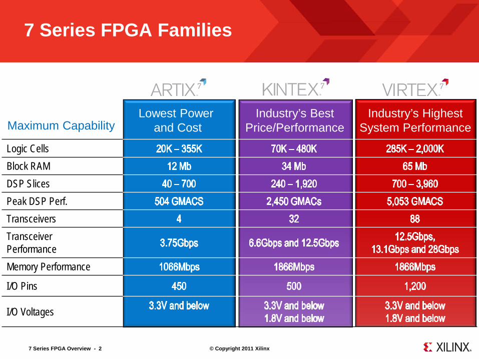
7 Series FPGA Families
Logic Cells Block RAM DSP Slices Peak DSP Perf. Transceivers Transceiver Performance Memory Performance
I/O Pins
I/O Voltages
Lowest Power and Cost
Industry’s Best Price/Performance
Industry’s Highest System Performance Maximum Capability
7 Series FPGA Overview - 3 © Copyright 2011 Xilinx
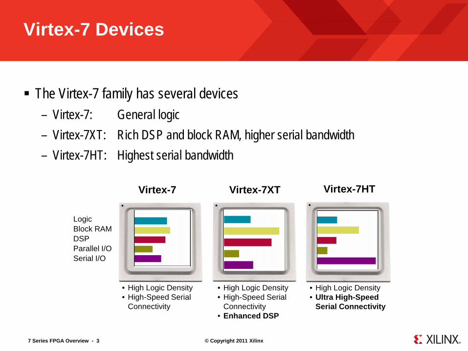
Virtex-7 Devices
The Virtex-7 family has several devices – Virtex-7: General logic – Virtex-7XT: Rich DSP and block RAM, higher serial bandwidth – Virtex-7HT: Highest serial bandwidth
Virtex-7XT Virtex-7 Virtex-7HT
• High Logic Density • High-Speed Serial
Connectivity
• High Logic Density • Ultra High-Speed
Serial Connectivity
• High Logic Density • High-Speed Serial
Connectivity • Enhanced DSP
Logic Block RAM DSP Parallel I/O Serial I/O
7 Series FPGA Overview - 4 © Copyright 2011 Xilinx
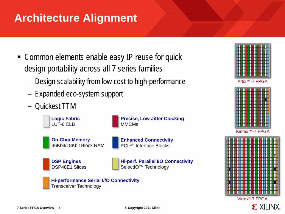
Architecture Alignment
Common elements enable easy IP reuse for quick design portability across all 7 series families – Design scalability from low-cost to high-performance – Expanded eco-system support – Quickest TTM
Precise, Low Jitter Clocking MMCMs
Logic Fabric LUT-6 CLB
DSP Engines DSP48E1 Slices
On-Chip Memory 36Kbit/18Kbit Block RAM
Enhanced Connectivity PCIe® Interface Blocks
Hi-perf. Parallel I/O Connectivity SelectIO™ Technology
Artix™-7 FPGA
Kintex™-7 FPGA
Virtex®-7 FPGA
Hi-performance Serial I//O Connectivity Transceiver Technology
7 Series FPGA Overview - 5 © Copyright 2011 Xilinx
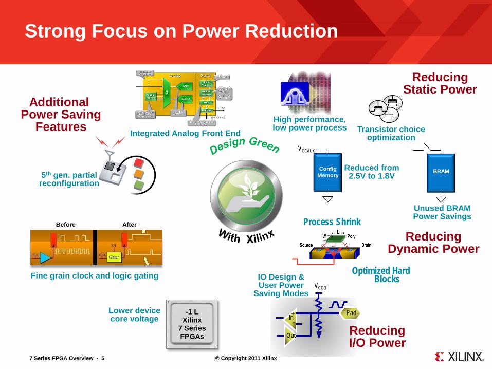
Strong Focus on Power Reduction
Unused BRAM Power Savings
BRAM
High performance, low power process Transistor choice
optimization
Config Memory
VCCAUX
Reduced from 2.5V to 1.8V
Reducing Static Power
Out
In Pad -
+
VCCO
IO Design & User Power
Saving Modes
Reducing I/O Power
Process Shrink Reducing
Dynamic Power Optimized Hard
Blocks Fine grain clock and logic gating
Lower device core voltage
-1 L Xilinx
7 Series FPGAs
Before After
5th gen. partial reconfiguration
Additional Power Saving
Features Integrated Analog Front End
7 Series FPGA Overview - 6 © Copyright 2011 Xilinx
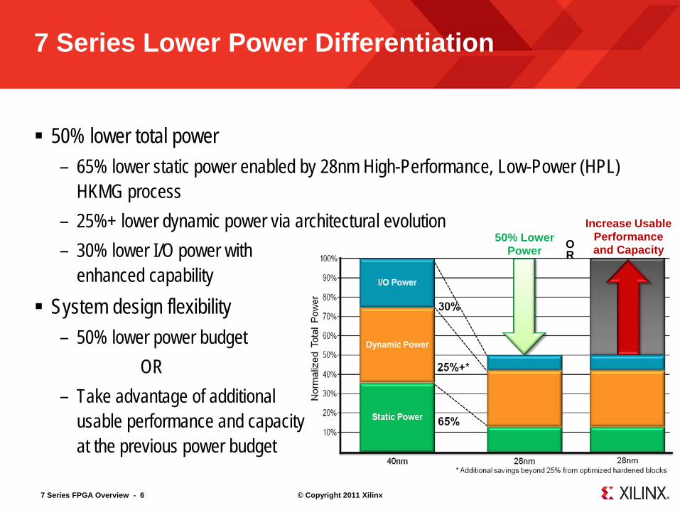
7 Series Lower Power Differentiation
50% lower total power – 65% lower static power enabled by 28nm High-Performance, Low-Power (HPL)
HKMG process – 25%+ lower dynamic power via architectural evolution – 30% lower I/O power with
enhanced capability System design flexibility
– 50% lower power budget OR – Take advantage of additional
usable performance and capacity at the previous power budget
50% Lower Power
Increase Usable Performance and Capacity O
R
7 Series FPGA Overview - 7 © Copyright 2011 Xilinx
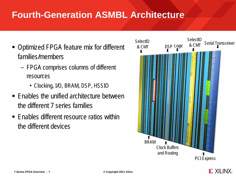
Fourth-Generation ASMBL Architecture
Optimized FPGA feature mix for different families/members – FPGA comprises columns of different
resources • Clocking, I/O, BRAM, DSP, HSSIO
Enables the unified architecture between the different 7 series families Enables different resource ratios within
the different devices
SelectIO & CMT Logic DSP
Serial Transceiver
BRAM Clock Buffers and Routing
PCI Express
SelectIO & CMT
7 Series FPGA Overview - 8 © Copyright 2011 Xilinx
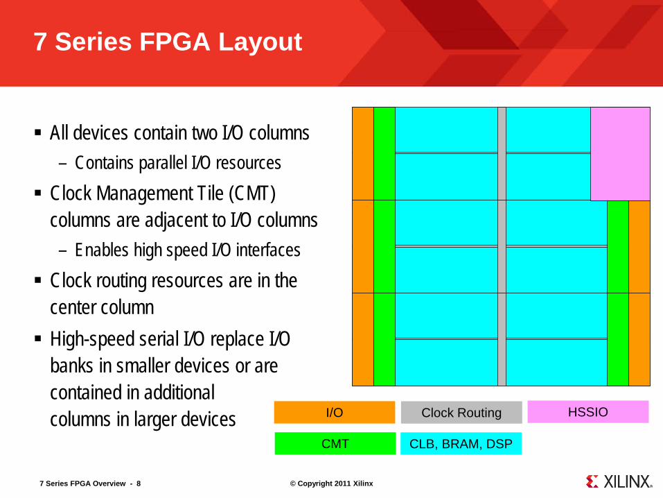
7 Series FPGA Layout
All devices contain two I/O columns – Contains parallel I/O resources
Clock Management Tile (CMT) columns are adjacent to I/O columns – Enables high speed I/O interfaces
Clock routing resources are in the center column High-speed serial I/O replace I/O
banks in smaller devices or are contained in additional columns in larger devices I/O
CMT
Clock Routing
CLB, BRAM, DSP
HSSIO
7 Series FPGA Overview - 9 © Copyright 2011 Xilinx
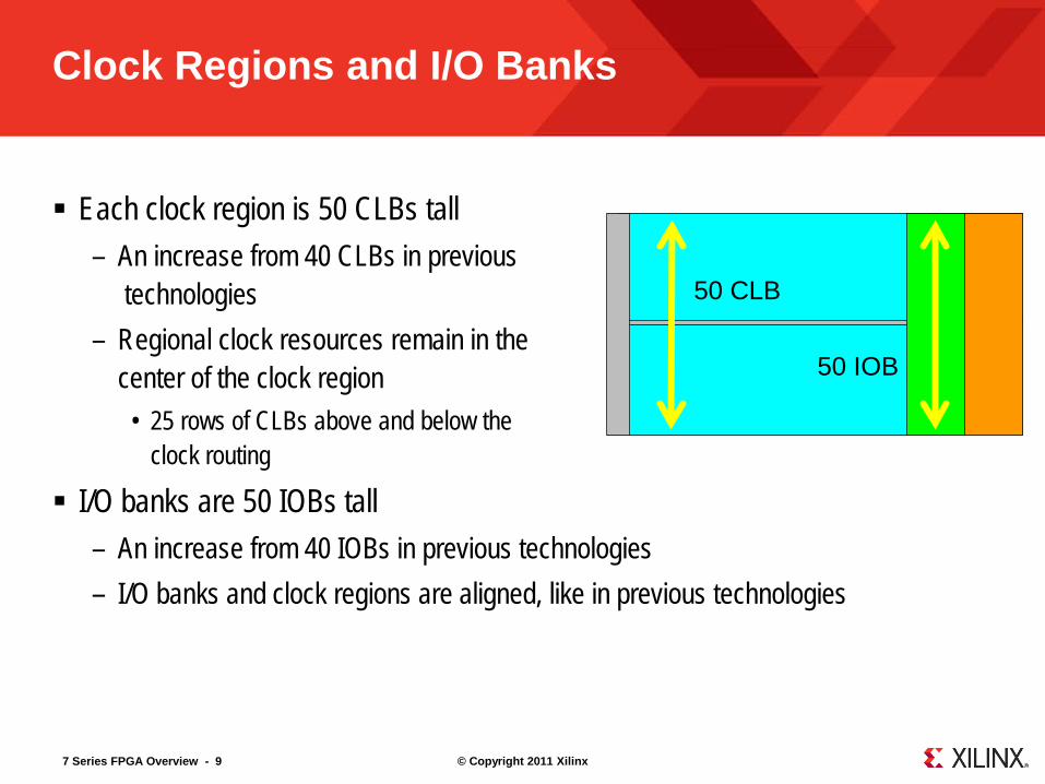
Clock Regions and I/O Banks
Each clock region is 50 CLBs tall – An increase from 40 CLBs in previous
technologies – Regional clock resources remain in the
center of the clock region • 25 rows of CLBs above and below the
clock routing
I/O banks are 50 IOBs tall – An increase from 40 IOBs in previous technologies – I/O banks and clock regions are aligned, like in previous technologies
50 CLB
50 IOB
7 Series FPGA Overview - 10 © Copyright 2011 Xilinx
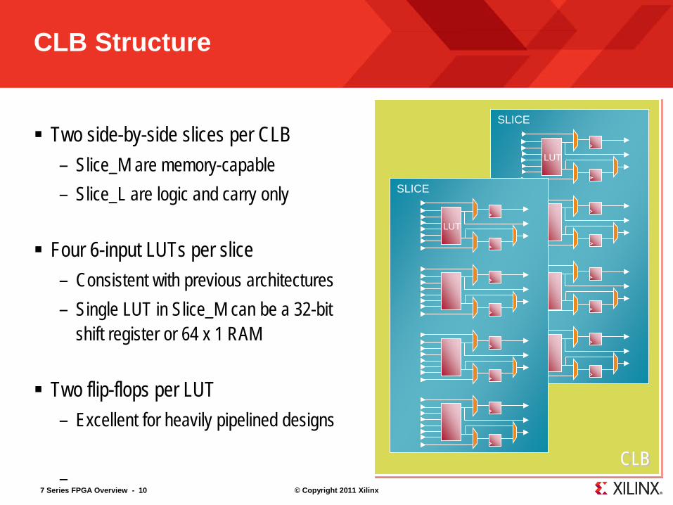
CLB Structure
Two side-by-side slices per CLB – Slice_M are memory-capable – Slice_L are logic and carry only
Four 6-input LUTs per slice
– Consistent with previous architectures – Single LUT in Slice_M can be a 32-bit
shift register or 64 x 1 RAM
Two flip-flops per LUT – Excellent for heavily pipelined designs
–
CLB
SLICE
LUT
SLICE
LUT
7 Series FPGA Overview - 11 © Copyright 2011 Xilinx
Block RAM
36K/18K block RAM – All Xilinx 7 series FPGA families use
same block RAM as Virtex-6 FPGAs Configurations same as Virtex-6 FPGAs
– 32k x 1 to 512 x 72 in one 36K block – Simple dual-port and true dual-port
configurations – Built-in FIFO logic – 64-bit error correction coding per 36K
block – Adjacent blocks combine to 64K x 1
without extra logic
36 DIA ADDRA 36
DOA Port A
36 Kb Memory
Array
CLKA WEA 4
36 DIB ADDRB 36
DOB
Port B CLKB WEB 4
7 Series FPGA Overview - 12 © Copyright 2011 Xilinx
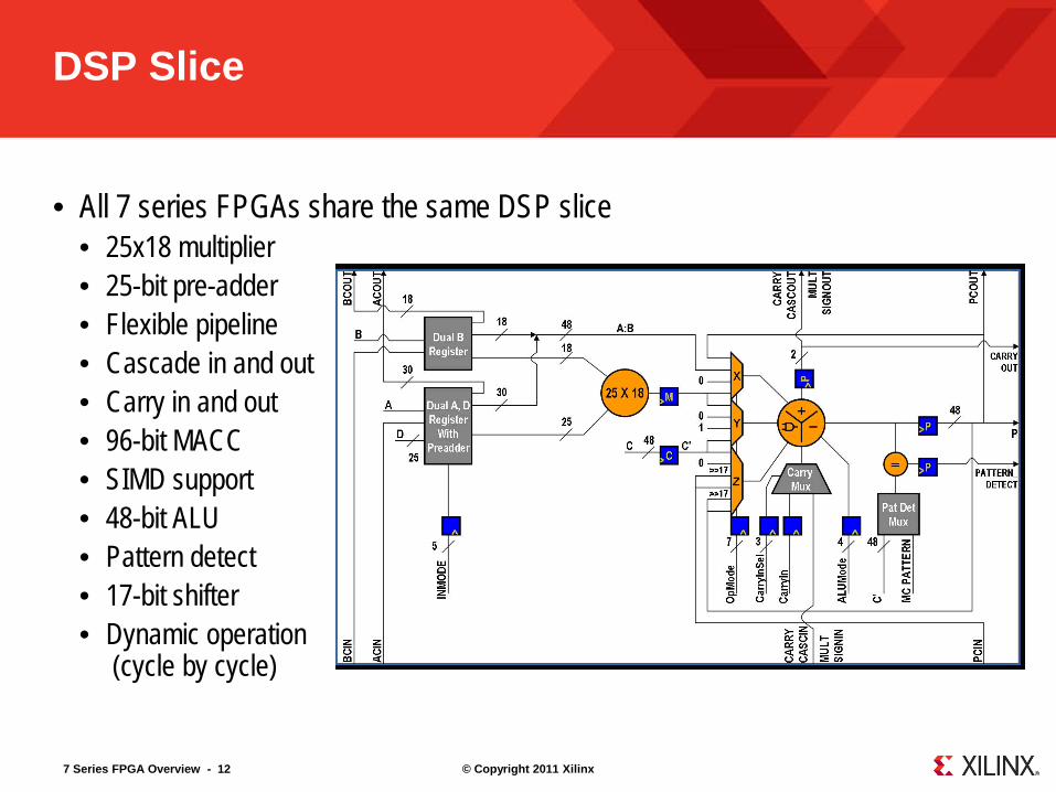
DSP Slice
• All 7 series FPGAs share the same DSP slice • 25x18 multiplier • 25-bit pre-adder • Flexible pipeline • Cascade in and out • Carry in and out • 96-bit MACC • SIMD support • 48-bit ALU • Pattern detect • 17-bit shifter • Dynamic operation
(cycle by cycle)
7 Series FPGA Overview - 13 © Copyright 2011 Xilinx
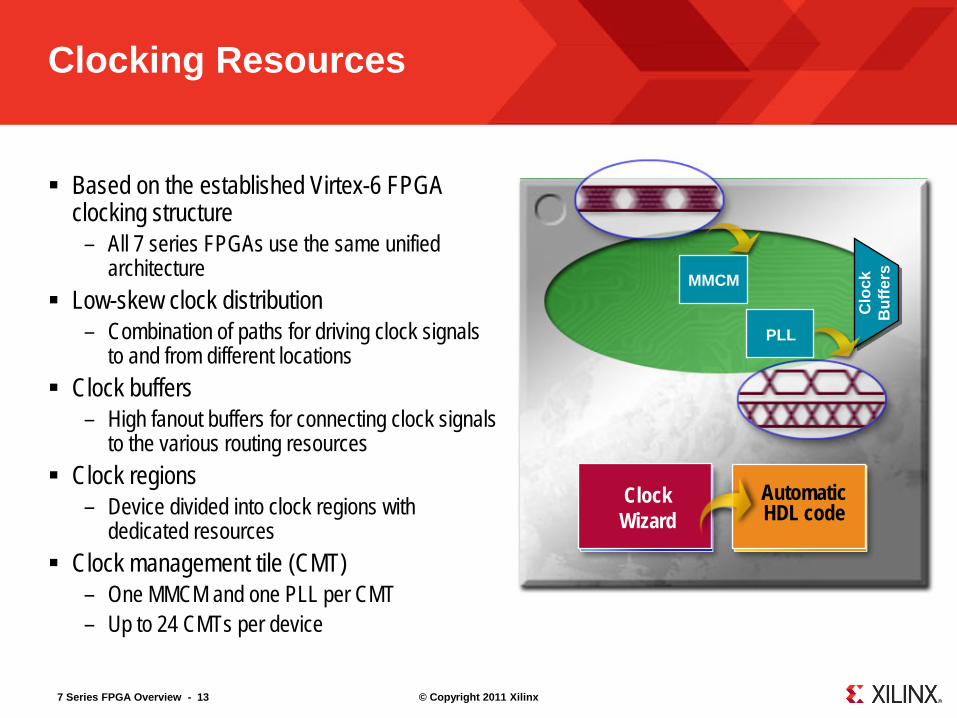
Clocking Resources
Based on the established Virtex-6 FPGA clocking structure
– All 7 series FPGAs use the same unified architecture
Low-skew clock distribution – Combination of paths for driving clock signals
to and from different locations Clock buffers
– High fanout buffers for connecting clock signals to the various routing resources
Clock regions – Device divided into clock regions with
dedicated resources Clock management tile (CMT)
– One MMCM and one PLL per CMT – Up to 24 CMTs per device
Clo
ck
Buf
fers
MMCM
PLL
Clock Wizard
Automatic HDL code
7 Series FPGA Overview - 14 © Copyright 2011 Xilinx
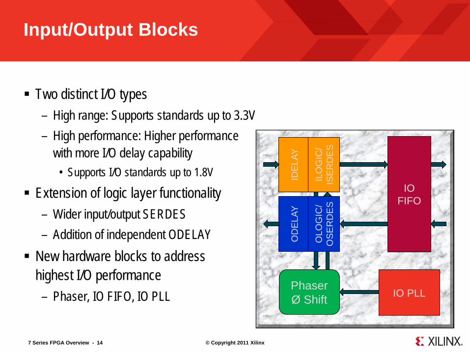
Input/Output Blocks
Two distinct I/O types – High range: Supports standards up to 3.3V – High performance: Higher performance
with more I/O delay capability • Supports I/O standards up to 1.8V
Extension of logic layer functionality – Wider input/output SERDES – Addition of independent ODELAY
New hardware blocks to address highest I/O performance – Phaser, IO FIFO, IO PLL IO PLL
IO FIFO
Phaser Ø Shift
IDE
LAY
ILO
GIC
/ IS
ER
DE
S
OD
ELA
Y
OLO
GIC
/ O
SE
RD
ES
7 Series FPGA Overview - 15 © Copyright 2011 Xilinx
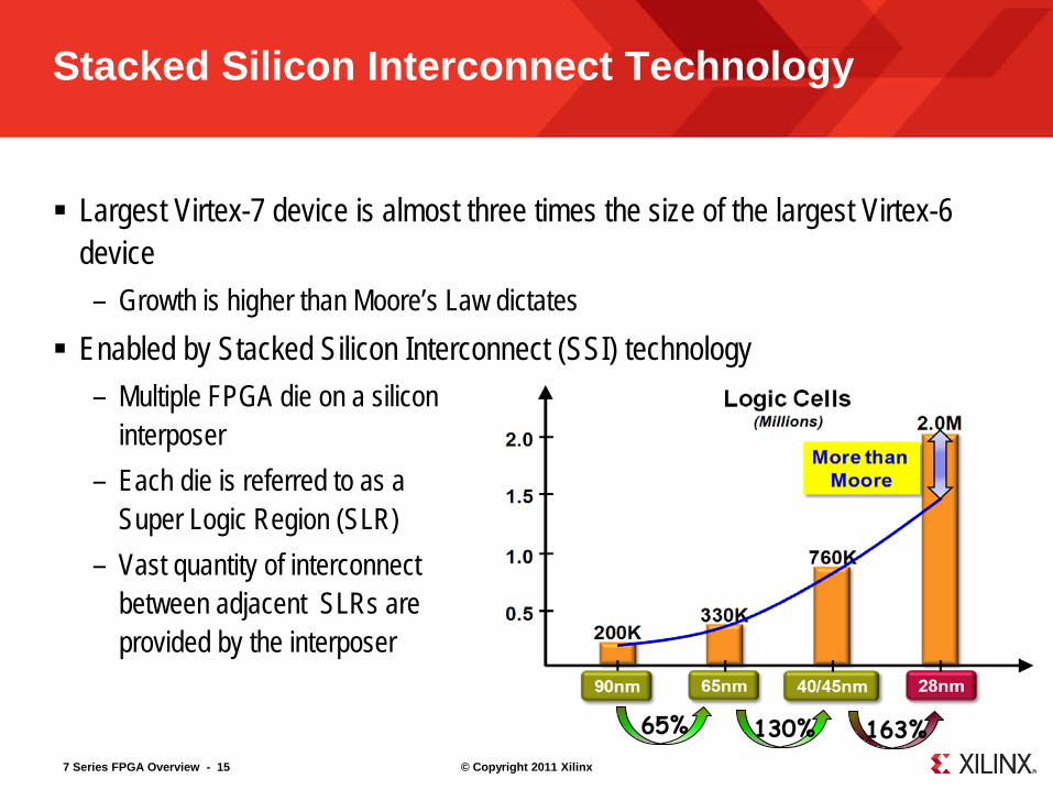
Stacked Silicon Interconnect Technology
Largest Virtex-7 device is almost three times the size of the largest Virtex-6 device – Growth is higher than Moore’s Law dictates
Enabled by Stacked Silicon Interconnect (SSI) technology – Multiple FPGA die on a silicon
interposer – Each die is referred to as a
Super Logic Region (SLR) – Vast quantity of interconnect
between adjacent SLRs are provided by the interposer
65% 130% 163%
7 Series FPGA Overview - 16 © Copyright 2011 Xilinx
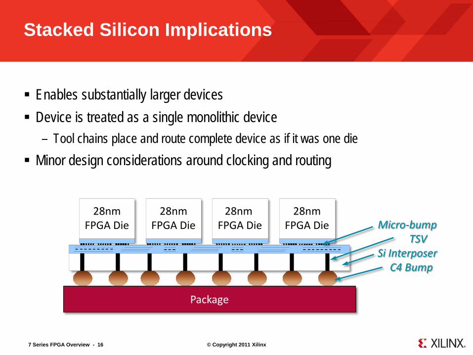
Stacked Silicon Implications
Enables substantially larger devices Device is treated as a single monolithic device
– Tool chains place and route complete device as if it was one die Minor design considerations around clocking and routing
Micro-bump TSV
Si Interposer C4 Bump
28nm FPGA Die
28nm FPGA Die
28nm FPGA Die
28nm FPGA Die
Package
7 Series FPGA Overview - 17 © Copyright 2011 Xilinx
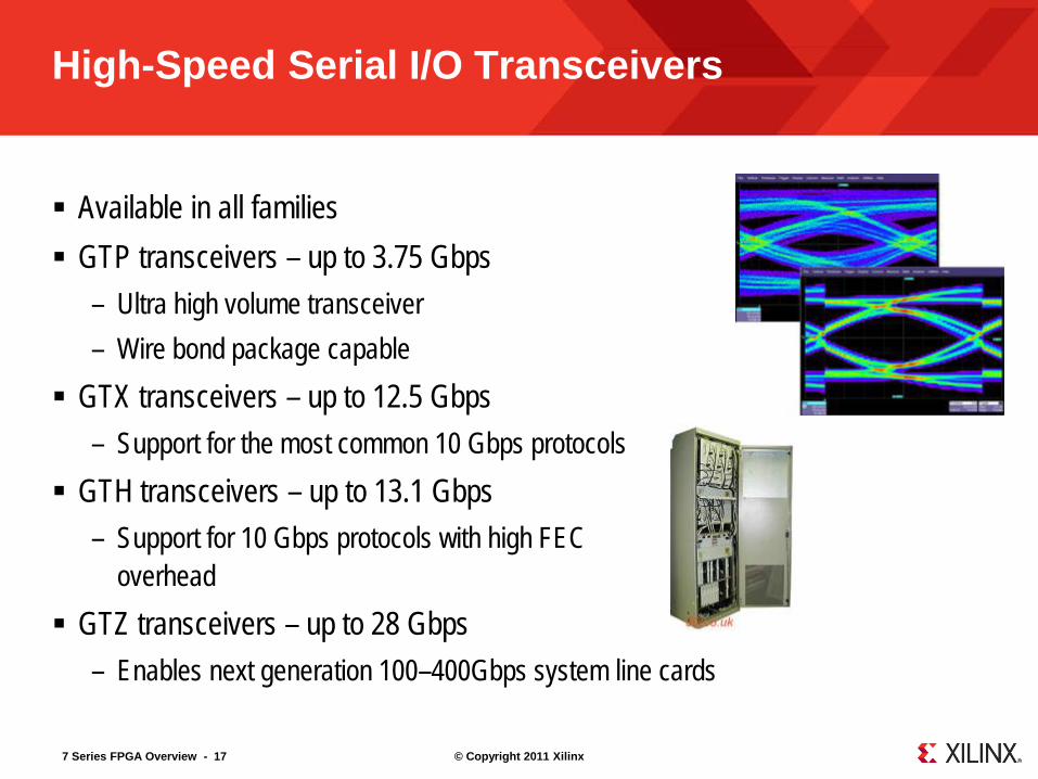
High-Speed Serial I/O Transceivers
Available in all families GTP transceivers – up to 3.75 Gbps
– Ultra high volume transceiver – Wire bond package capable
GTX transceivers – up to 12.5 Gbps – Support for the most common 10 Gbps protocols
GTH transceivers – up to 13.1 Gbps – Support for 10 Gbps protocols with high FEC
overhead GTZ transceivers – up to 28 Gbps
– Enables next generation 100–400Gbps system line cards
7 Series FPGA Overview - 18 © Copyright 2011 Xilinx
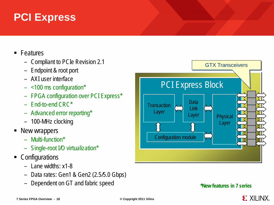
PCI Express
Features – Compliant to PCIe Revision 2.1 – Endpoint & root port – AXI user interface – <100 ms configuration* – FPGA configuration over PCI Express* – End-to-end CRC* – Advanced error reporting* – 100-MHz clocking
New wrappers – Multi-function* – Single-root I/O virtualization*
Configurations – Lane widths: x1-8 – Data rates: Gen1 & Gen2 (2.5/5.0 Gbps) – Dependent on GT and fabric speed
Physical Layer
Data Link
Layer
Transaction Layer
Configuration module
PCI Express Block
GTX Transceivers
*New features in 7 series
7 Series FPGA Overview - 19 © Copyright 2011 Xilinx
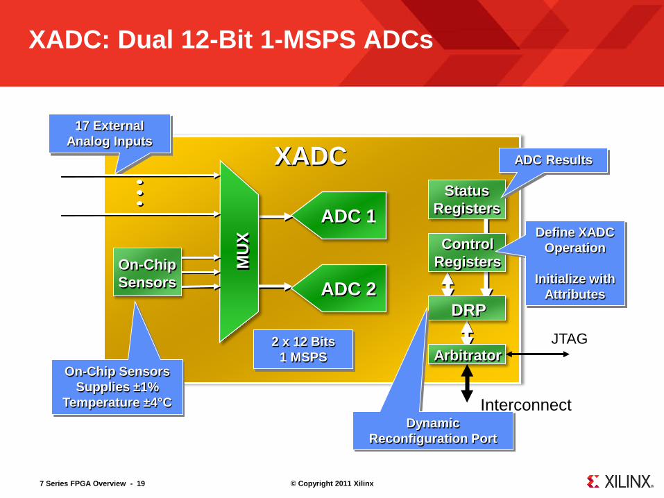
XADC: Dual 12-Bit 1-MSPS ADCs
17 External Analog Inputs
On-Chip Sensors Supplies ±1%
Temperature ±4°C
ADC 1 M
UX
ADC Results XADC
Arbitrator
DRP
Dynamic Reconfiguration Port
Define XADC Operation
Initialize with
Attributes ADC 2
2 x 12 Bits 1 MSPS
Interconnect
JTAG
Status Registers
Control Registers On-Chip
Sensors
7 Series FPGA Overview - 20 © Copyright 2011 Xilinx
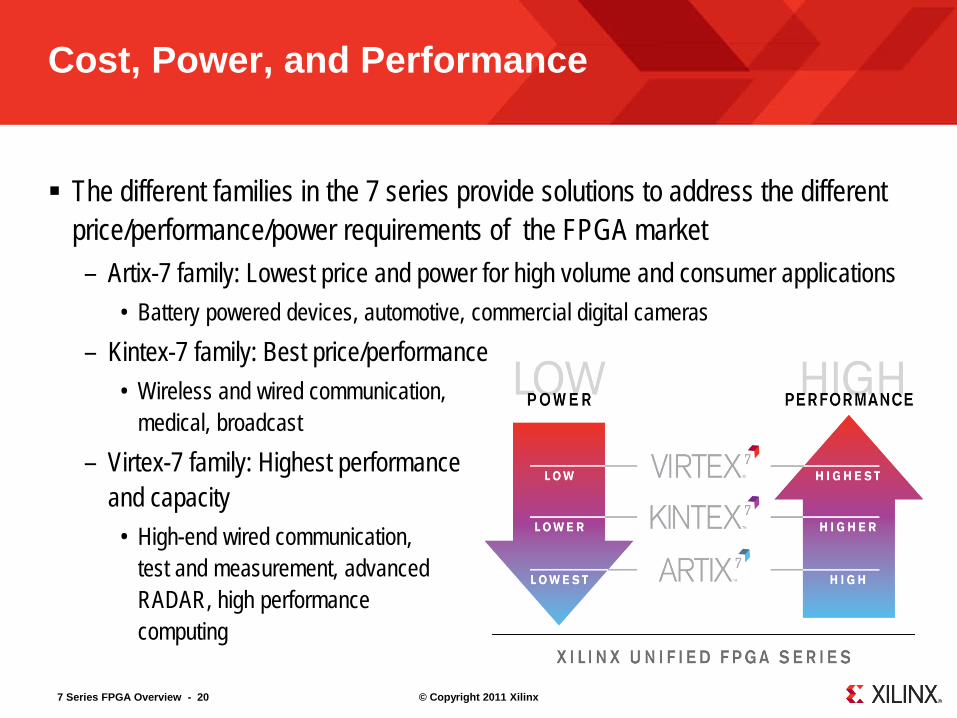
Cost, Power, and Performance
The different families in the 7 series provide solutions to address the different price/performance/power requirements of the FPGA market – Artix-7 family: Lowest price and power for high volume and consumer applications
• Battery powered devices, automotive, commercial digital cameras – Kintex-7 family: Best price/performance
• Wireless and wired communication, medical, broadcast
– Virtex-7 family: Highest performance and capacity
• High-end wired communication, test and measurement, advanced RADAR, high performance computing
7 Series FPGA Overview - 21 © Copyright 2011 Xilinx
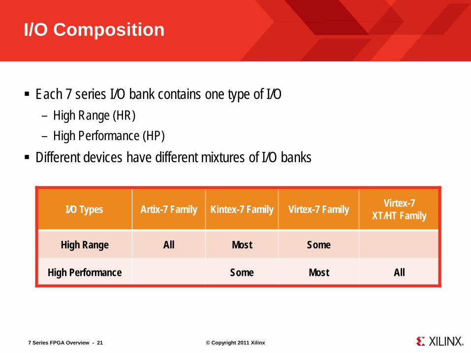
I/O Composition
Each 7 series I/O bank contains one type of I/O – High Range (HR) – High Performance (HP)
Different devices have different mixtures of I/O banks
I/O Types Artix-7 Family Kintex-7 Family Virtex-7 Family Virtex-7 XT/HT Family
High Range All Most Some
High Performance Some Most All
7 Series FPGA Overview - 22 © Copyright 2011 Xilinx
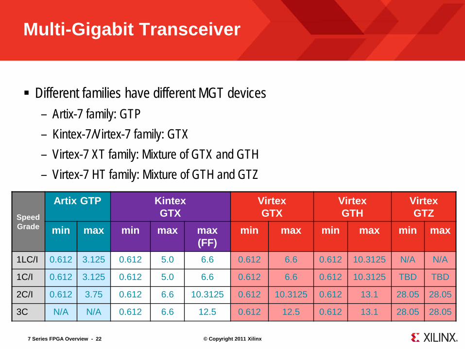
Multi-Gigabit Transceiver
Different families have different MGT devices – Artix-7 family: GTP – Kintex-7/Virtex-7 family: GTX – Virtex-7 XT family: Mixture of GTX and GTH – Virtex-7 HT family: Mixture of GTH and GTZ
Speed Grade
Artix GTP Kintex GTX
Virtex GTX
Virtex GTH
Virtex GTZ
min max min max max (FF)
min max min max min max
1LC/I 0.612 3.125 0.612 5.0 6.6 0.612 6.6 0.612 10.3125 N/A N/A
1C/I 0.612 3.125 0.612 5.0 6.6 0.612 6.6 0.612 10.3125 TBD TBD
2C/I 0.612 3.75 0.612 6.6 10.3125 0.612 10.3125 0.612 13.1 28.05 28.05
3C N/A N/A 0.612 6.6 12.5 0.612 12.5 0.612 13.1 28.05 28.05
7 Series FPGA Overview - 23 © Copyright 2011 Xilinx
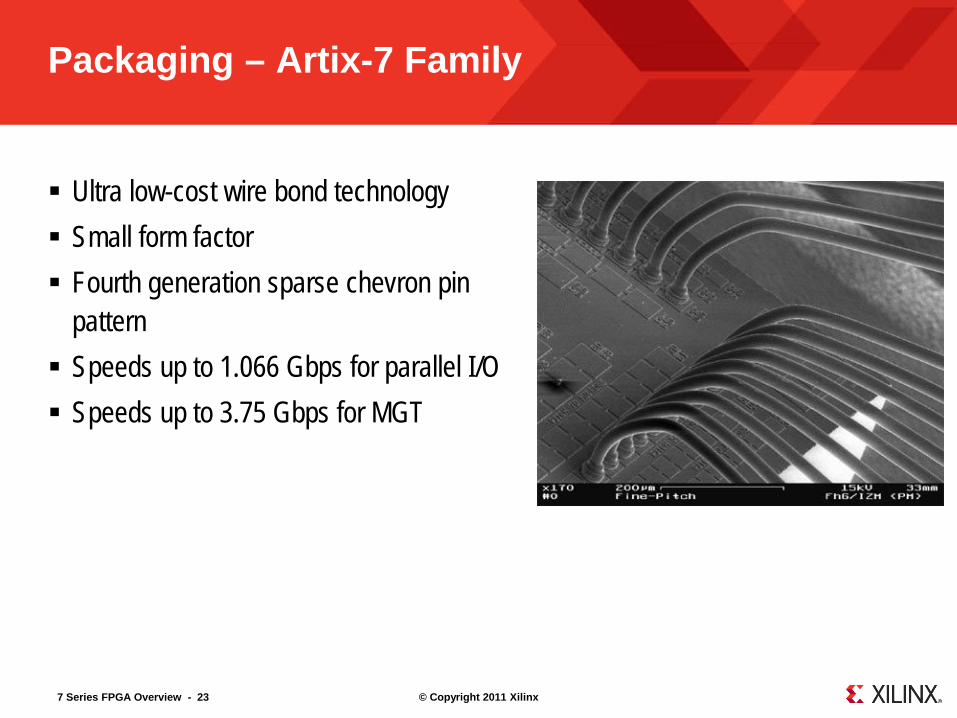
Packaging – Artix-7 Family
Ultra low-cost wire bond technology Small form factor Fourth generation sparse chevron pin
pattern Speeds up to 1.066 Gbps for parallel I/O Speeds up to 3.75 Gbps for MGT
7 Series FPGA Overview - 24 © Copyright 2011 Xilinx
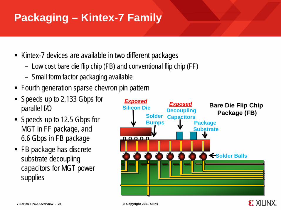
Packaging – Kintex-7 Family
Kintex-7 devices are available in two different packages – Low cost bare die flip chip (FB) and conventional flip chip (FF) – Small form factor packaging available
Fourth generation sparse chevron pin pattern Speeds up to 2.133 Gbps for
parallel I/O Speeds up to 12.5 Gbps for
MGT in FF package, and 6.6 Gbps in FB package
FB package has discrete substrate decoupling capacitors for MGT power supplies
o o o o o
Exposed Silicon Die
Package Substrate
Solder Bumps
Solder Balls
Exposed Decoupling Capacitors
Bare Die Flip Chip Package (FB)
7 Series FPGA Overview - 25 © Copyright 2011 Xilinx
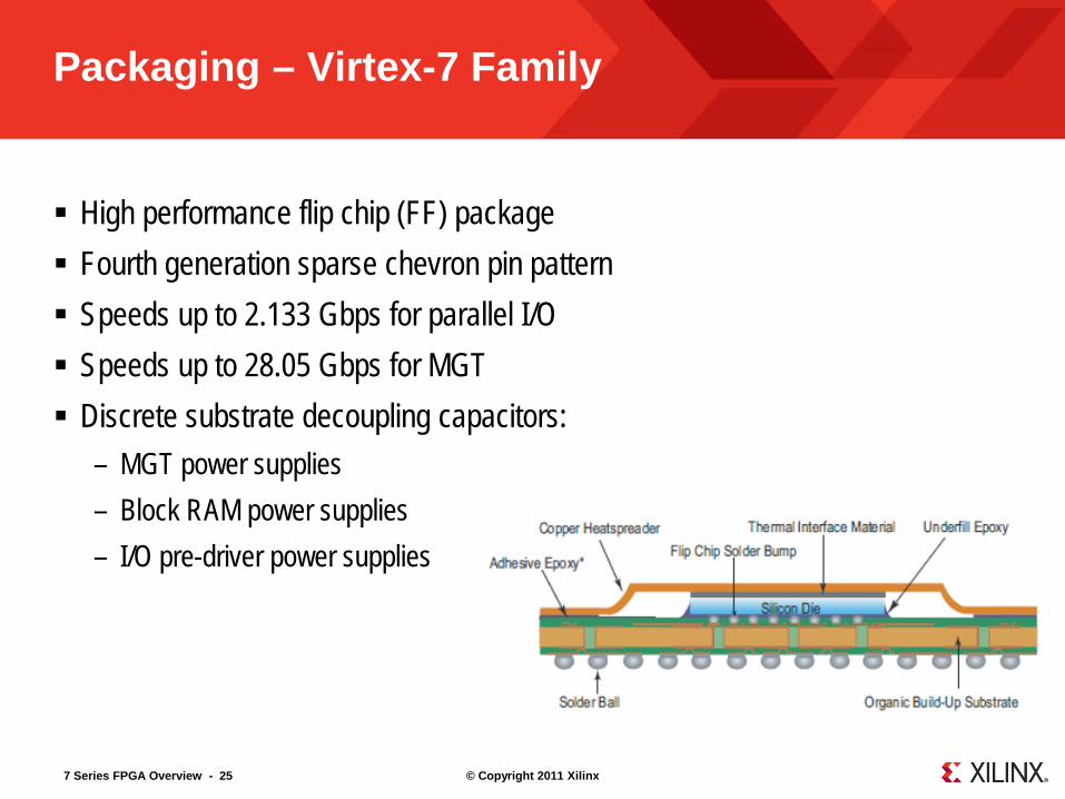
Packaging – Virtex-7 Family
High performance flip chip (FF) package Fourth generation sparse chevron pin pattern Speeds up to 2.133 Gbps for parallel I/O Speeds up to 28.05 Gbps for MGT Discrete substrate decoupling capacitors:
– MGT power supplies – Block RAM power supplies – I/O pre-driver power supplies

7 Series FPGA Overview - 26 © Copyright 2011 Xilinx
Where Can I Learn More?
Xilinx Education Services courses www.xilinx.com/training – Designing with 7-Series Device Families course
• How to get the most out of both device families • How to build the best HDL code for your FPGA design • How to optimize your design for Spartan-6 and/or Virtex-6 • How to take advantage of the newest device features
Free Video Based Training – Part 1,2, and 3 of the 7 Series FPGA Overview – How Do I Plan to Power My FPGA? – What are the Spartan-6 Power Management Features? – What are the Virtex-6 Power Management Features? – Basic FPGA Configuration, Parts 1 and 2