56-Ball MCP Combination Memory Parallel NOR and...
128
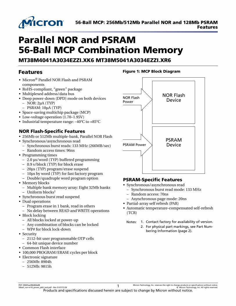
Parallel NOR and PSRAM 56-Ball MCP Combination Memory MT38M4041A3034EZZI.XK6 MT38M5041A3034EZZI.XR6 Features • Micron ® Parallel NOR Flash and PSRAM components • RoHS-compliant, “green” package • Multiplexed address/data bus • Deep power-down (DPD) mode on both devices – NOR: 2μA (TYP) – PSRAM: 10μA (TYP) • Space-saving multichip package (MCP) • Low-voltage operation (1.70–1.95V) • Industrial temperature range: –40°C to +85°C NOR Flash-Specific Features • 256Mb or 512Mb multiple-bank, Parallel NOR Flash • Synchronous/asynchronous read – Synchronous burst reads: 133 MHz (266MB/sec) – Random access times: 96ns • Programming times – 2.0 μs/word (TYP) buffered programming – 0.9 s/block (TYP) for block erase – 20μs (TYP) program/erase suspend – 10μs by word (TYP) for fast factory program – Double/quadruple word program option • Memory blocks – Multiple bank memory array: Eight 32Mb banks – Uniform blocks 1 • Synchronous burst read suspend • Dual operations – Program erase in 1 bank, read in others – No delay between READ and WRITE operations • Block locking – All blocks locked at power-up – Any combination of blocks can be locked – WP# for block lock-down • Security – 2112-bit user programmable OTP cells – 64-bit unique device number • Common Flash interface • 100,000 PROGRAM/ERASE cycles per block • Electronic signature – 256Mb: 8904h – 512Mb: 9815h Figure 1: MCP Block Diagram NOR Flash Device NOR Flash Power PSRAM Power PSRAM Device PSRAM-Specific Features • Synchronous/asynchronous read – Synchronous burst read mode: 133 MHz – Random access: 70ns – Asynchronous page mode: 20ns • Partial-array self refresh (PAR) • Automatic temperature-compensated self-refresh (TCR) Notes: 1. Contact factory for availability of version. 2. For physical part markings, see Part Num- bering Information (page 2). 56-Ball MCP: 256Mb/512Mb Parallel NOR and 128Mb PSRAM Features PDF: 09005aef86484a88 56ball_nor-m18_psram_jxk6_jxr6.pdf - Rev. B 07/15 EN 1 Micron Technology, Inc. reserves the right to change products or specifications without notice. © Micron Technology, Inc. All rights reserved. Products and specifications discussed herein are subject to change by Micron without notice.
Transcript of 56-Ball MCP Combination Memory Parallel NOR and...
Parallel NOR and PSRAM56-Ball MCP Combination MemoryMT38M4041A3034EZZI.XK6 MT38M5041A3034EZZI.XR6
Features• Micron® Parallel NOR Flash and PSRAM
components• RoHS-compliant, “green” package• Multiplexed address/data bus• Deep power-down (DPD) mode on both devices
– NOR: 2μA (TYP)– PSRAM: 10μA (TYP)
• Space-saving multichip package (MCP)• Low-voltage operation (1.70–1.95V)• Industrial temperature range: –40°C to +85°C
NOR Flash-Specific Features• 256Mb or 512Mb multiple-bank, Parallel NOR Flash• Synchronous/asynchronous read
– Synchronous burst reads: 133 MHz (266MB/sec)– Random access times: 96ns
• Programming times– 2.0 μs/word (TYP) buffered programming– 0.9 s/block (TYP) for block erase– 20μs (TYP) program/erase suspend– 10μs by word (TYP) for fast factory program– Double/quadruple word program option
• Memory blocks– Multiple bank memory array: Eight 32Mb banks– Uniform blocks1
• Synchronous burst read suspend• Dual operations
– Program erase in 1 bank, read in others– No delay between READ and WRITE operations
• Block locking– All blocks locked at power-up– Any combination of blocks can be locked– WP# for block lock-down
• Security– 2112-bit user programmable OTP cells– 64-bit unique device number
• Common Flash interface• 100,000 PROGRAM/ERASE cycles per block• Electronic signature
– 256Mb: 8904h– 512Mb: 9815h
Figure 1: MCP Block Diagram
NOR FlashDeviceNOR Flash
Power
PSRAM PowerPSRAMDevice
PSRAM-Specific Features• Synchronous/asynchronous read
– Synchronous burst read mode: 133 MHz– Random access: 70ns– Asynchronous page mode: 20ns
• Partial-array self refresh (PAR)• Automatic temperature-compensated self-refresh
(TCR)
Notes: 1. Contact factory for availability of version.2. For physical part markings, see Part Num-
bering Information (page 2).
56-Ball MCP: 256Mb/512Mb Parallel NOR and 128Mb PSRAMFeatures
PDF: 09005aef86484a8856ball_nor-m18_psram_jxk6_jxr6.pdf - Rev. B 07/15 EN 1 Micron Technology, Inc. reserves the right to change products or specifications without notice.
© Micron Technology, Inc. All rights reserved.
Products and specifications discussed herein are subject to change by Micron without notice.
Part Numbering Information
Micron NOR Flash and PSRAM devices are available in different configurations and densities. The MCP/PoP partnumbering guide is available at www.micron.com/numbering.
Figure 2: Part Number Chart
MT 38W 203 1 A 9 0
Micron Technology
Product Family38L = L-Series NOR + xNAND + xDRAM38M = M-Series NOR + xNAND + xDRAM38W = W-Series NOR + xNAND + xDRAM38Q = Q-Series NOR + xNAND + xDRAM
NOR Density1 = 32Mb2 = 64Mb3 = 128Mb4 = 256Mb5 = 512Mb7 = 1Gb
NAND Density0 = N/A
RAM Density1 = 16Mb2 = 32Mb3 = 64Mb4 = 128Mb5 = 256Mb7 = 512Mb
Voltage Range (Core I/O)1 = 1.8V for Core and I/O
Die CountA = 1 NOR + 1 xDRAM
NOR Configuration3 = Uniform boot, A/D, AA/D* MUX5 = Bottom boot, no MUX6 = Bottom boot, A/D MUX9 = Top boot, no MUXA = Top boot, A/D MUX
*AA/D interface configurable through register
2
Production StatusBlank = ProductionES = Engineering sampleMS = Mechanical sample
Die Revision CodeContact factory
Operating Temperature RangeI = Industrail (–40°C to 85°C)W = Wireless (–25°C to 85°C)
Special OptionContact factory
Package CodeZAx = 44-ball VFBGA, 7.5mm x 5mm x 1mm, F10x4 + 4, 0.53JZ = 52-ball VFBGA, 6mm x 4mm x 1.2mm, F10x6 - 8, 0.5, B.3ZSx = 56-ball VFBGA, 8mm x 6mm x 1mm, 10x6 - 8 + 4, 0.5, B.3JVZ = 56-ball TFBGA, 8mm x 6mm x 1.2mm, F10x6 - 8 + 4, 0.5, B.34EZ = 56-ball VFBGA, 8mm x 8mm x 1mm, 0.519Z = 64-ball VFBGA, 7.7mm x 9mm x 1mm, F10x6 + 4, p.5, B.3ZQx = 88-ball TFBGA, 8mm x 10mm x 1.2mm, F8x10 + 8, 0.83RZ = 133-ball VFBGA, 8mm x 8mm x 1mm, 3R14x14 + 1, 0.5
xLPDRAM Description0 = N/A1 = Async PSRAM2 = Sync PSRAM, no MUX3 = Sync PSRAM, A/D MUX6 = x16 DDR, 2K page8 = x32 DDR, 4K pageY = Async PSRAM, no page mode
xNAND Description0 = None
ZQx Z W XQ5. - ES
Device Marking
Due to the size of the package, the Micron-standard part number is not printed on the top of the device. Instead,an abbreviated device mark consisting of a 5-digit alphanumeric code is used. The abbreviated device marks arecross-referenced to the Micron part numbers at the FBGA Part Marking Decoder site: www.micron.com/decoder.To view the location of the abbreviated mark on the device, refer to customer service note CSN-11, “Product Mark/Label,” at www.micron.com/csn.
56-Ball MCP: 256Mb/512Mb Parallel NOR and 128Mb PSRAMFeatures
PDF: 09005aef86484a8856ball_nor-m18_psram_jxk6_jxr6.pdf - Rev. B 07/15 EN 2 Micron Technology, Inc. reserves the right to change products or specifications without notice.
© Micron Technology, Inc. All rights reserved.
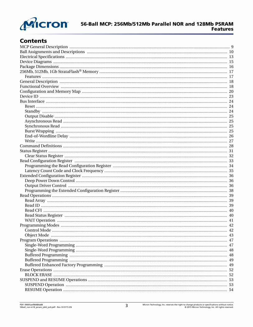
ContentsMCP General Description ................................................................................................................................. 9Ball Assignments and Descriptions ................................................................................................................. 10Electrical Specifications .................................................................................................................................. 13Device Diagrams ............................................................................................................................................ 15Package Dimensions ....................................................................................................................................... 16256Mb, 512Mb, 1Gb StrataFlash® Memory ....................................................................................................... 17
Features ..................................................................................................................................................... 17General Description ....................................................................................................................................... 18Functional Overview ...................................................................................................................................... 18Configuration and Memory Map ..................................................................................................................... 20Device ID ....................................................................................................................................................... 23Bus Interface .................................................................................................................................................. 24
Reset .......................................................................................................................................................... 24Standby ..................................................................................................................................................... 24Output Disable ........................................................................................................................................... 25Asynchronous Read .................................................................................................................................... 25Synchronous Read ...................................................................................................................................... 25Burst Wrapping .......................................................................................................................................... 25End-of-Wordline Delay ............................................................................................................................... 26Write .......................................................................................................................................................... 27
Command Definitions .................................................................................................................................... 28Status Register ................................................................................................................................................ 31
Clear Status Register ................................................................................................................................... 32Read Configuration Register ........................................................................................................................... 33
Programming the Read Configuration Register ............................................................................................ 34Latency Count Code and Clock Frequency ................................................................................................... 35
Extended Configuration Register ..................................................................................................................... 36Deep Power Down Control .......................................................................................................................... 36Output Driver Control ................................................................................................................................ 36Programming the Extended Configuration Register ...................................................................................... 38
Read Operations ............................................................................................................................................. 39Read Array ................................................................................................................................................. 39Read ID ...................................................................................................................................................... 39Read CFI .................................................................................................................................................... 40Read Status Register ................................................................................................................................... 40WAIT Operation ......................................................................................................................................... 41
Programming Modes ...................................................................................................................................... 42Control Mode ............................................................................................................................................. 42Object Mode .............................................................................................................................................. 43
Program Operations ....................................................................................................................................... 47Single-Word Programming .......................................................................................................................... 47Single-Word Programming .......................................................................................................................... 48Buffered Programming ............................................................................................................................... 48Buffered Programming ............................................................................................................................... 49Buffered Enhanced Factory Programming ................................................................................................... 49
Erase Operations ............................................................................................................................................ 52BLOCK ERASE ............................................................................................................................................ 52
SUSPEND and RESUME Operations ................................................................................................................ 53SUSPEND Operation .................................................................................................................................. 53RESUME Operation .................................................................................................................................... 54
56-Ball MCP: 256Mb/512Mb Parallel NOR and 128Mb PSRAMFeatures
PDF: 09005aef86484a8856ball_nor-m18_psram_jxk6_jxr6.pdf - Rev. B 07/15 EN 3 Micron Technology, Inc. reserves the right to change products or specifications without notice.
© 2015 Micron Technology, Inc. All rights reserved.
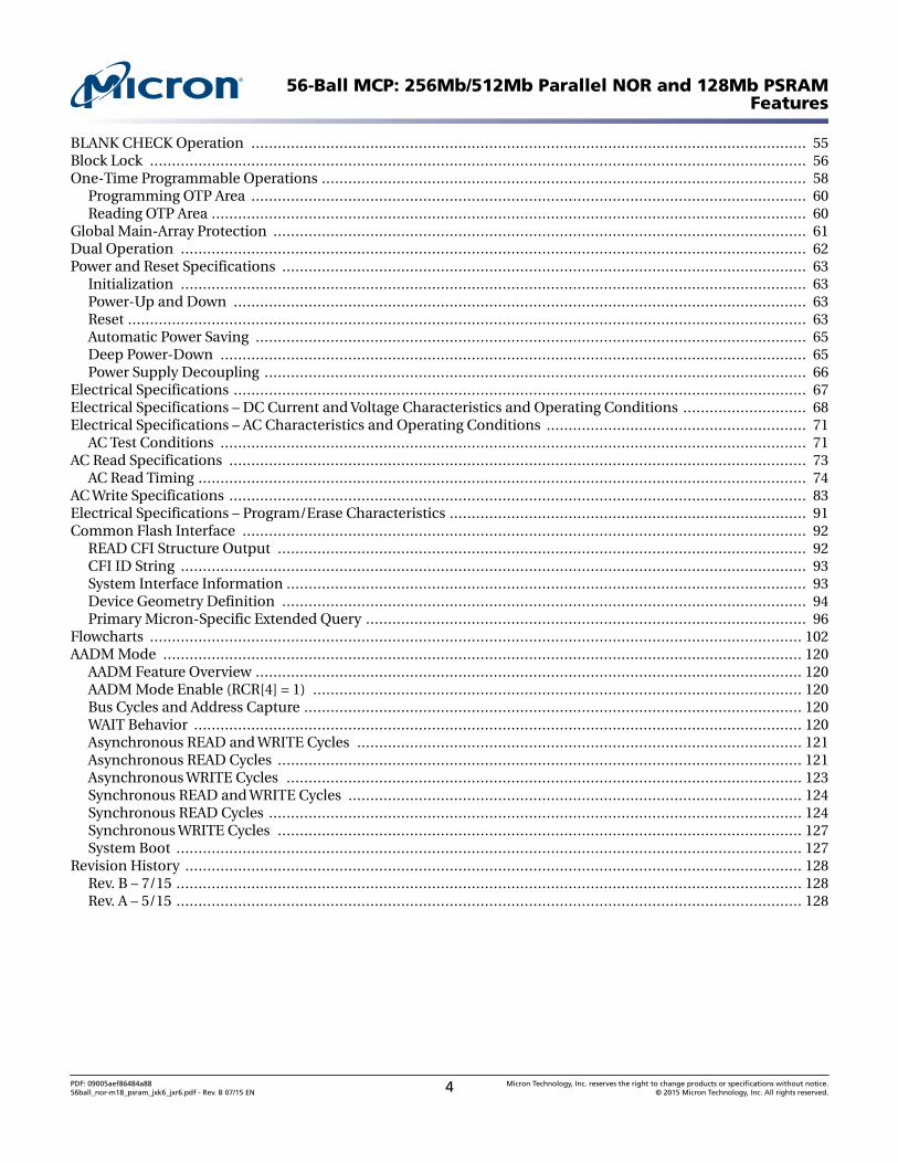
BLANK CHECK Operation .............................................................................................................................. 55Block Lock ..................................................................................................................................................... 56One-Time Programmable Operations .............................................................................................................. 58
Programming OTP Area .............................................................................................................................. 60Reading OTP Area ....................................................................................................................................... 60
Global Main-Array Protection ......................................................................................................................... 61Dual Operation .............................................................................................................................................. 62Power and Reset Specifications ....................................................................................................................... 63
Initialization .............................................................................................................................................. 63Power-Up and Down .................................................................................................................................. 63Reset .......................................................................................................................................................... 63Automatic Power Saving ............................................................................................................................. 65Deep Power-Down ..................................................................................................................................... 65Power Supply Decoupling ........................................................................................................................... 66
Electrical Specifications .................................................................................................................................. 67Electrical Specifications – DC Current and Voltage Characteristics and Operating Conditions ............................ 68Electrical Specifications – AC Characteristics and Operating Conditions ........................................................... 71
AC Test Conditions ..................................................................................................................................... 71AC Read Specifications ................................................................................................................................... 73
AC Read Timing .......................................................................................................................................... 74AC Write Specifications ................................................................................................................................... 83Electrical Specifications – Program/Erase Characteristics ................................................................................. 91Common Flash Interface ................................................................................................................................ 92
READ CFI Structure Output ........................................................................................................................ 92CFI ID String .............................................................................................................................................. 93System Interface Information ...................................................................................................................... 93Device Geometry Definition ....................................................................................................................... 94Primary Micron-Specific Extended Query .................................................................................................... 96
Flowcharts .................................................................................................................................................... 102AADM Mode ................................................................................................................................................. 120
AADM Feature Overview ............................................................................................................................ 120AADM Mode Enable (RCR[4] = 1) ............................................................................................................... 120Bus Cycles and Address Capture ................................................................................................................. 120WAIT Behavior .......................................................................................................................................... 120Asynchronous READ and WRITE Cycles ..................................................................................................... 121Asynchronous READ Cycles ....................................................................................................................... 121Asynchronous WRITE Cycles ..................................................................................................................... 123Synchronous READ and WRITE Cycles ....................................................................................................... 124Synchronous READ Cycles ......................................................................................................................... 124Synchronous WRITE Cycles ....................................................................................................................... 127System Boot .............................................................................................................................................. 127
Revision History ............................................................................................................................................ 128Rev. B – 7/15 .............................................................................................................................................. 128Rev. A – 5/15 .............................................................................................................................................. 128
56-Ball MCP: 256Mb/512Mb Parallel NOR and 128Mb PSRAMFeatures
PDF: 09005aef86484a8856ball_nor-m18_psram_jxk6_jxr6.pdf - Rev. B 07/15 EN 4 Micron Technology, Inc. reserves the right to change products or specifications without notice.
© 2015 Micron Technology, Inc. All rights reserved.
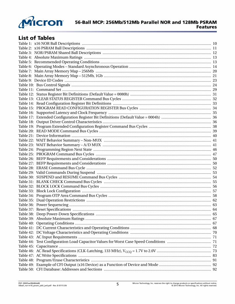
List of TablesTable 1: x16 NOR Ball Descriptions ................................................................................................................ 10Table 2: x16 PSRAM Ball Descriptions ............................................................................................................ 11Table 3: NOR/PSRAM Shared Ball Descriptions .............................................................................................. 12Table 4: Absolute Maximum Ratings .............................................................................................................. 13Table 5: Recommended Operating Conditions ................................................................................................ 13Table 6: Operating Modes – Standard Asynchronous Operation ....................................................................... 14Table 7: Main Array Memory Map – 256Mb .................................................................................................... 20Table 8: Main Array Memory Map – 512Mb, 1Gb ............................................................................................. 21Table 9: Device ID Codes ............................................................................................................................... 23Table 10: Bus Control Signals ......................................................................................................................... 24Table 11: Command Set ................................................................................................................................. 29Table 12: Status Register Bit Definitions (Default Value = 0080h) ...................................................................... 31Table 13: CLEAR STATUS REGISTER Command Bus Cycles ............................................................................. 32Table 14: Read Configuration Register Bit Definitions ..................................................................................... 33Table 15: PROGRAM READ CONFIGURATION REGISTER Bus Cycles .............................................................. 34Table 16: Supported Latency and Clock Frequency ......................................................................................... 35Table 17: Extended Configuration Register Bit Definitions (Default Value = 0004h) ........................................... 36Table 18: Output Driver Control Characteristics .............................................................................................. 36Table 19: Program Extended Configuration Register Command Bus Cycles ...................................................... 38Table 20: READ MODE Command Bus Cycles ................................................................................................. 39Table 21: Device Information ......................................................................................................................... 40Table 22: WAIT Behavior Summary – Non-MUX ............................................................................................. 41Table 23: WAIT Behavior Summary – A/D MUX .............................................................................................. 41Table 24: Programming Region Next State ...................................................................................................... 46Table 25: PROGRAM Command Bus Cycles .................................................................................................... 47Table 26: BEFP Requirements and Considerations .......................................................................................... 50Table 27: BEFP Requirements and Considerations .......................................................................................... 50Table 28: ERASE Command Bus Cycle ............................................................................................................ 52Table 29: Valid Commands During Suspend ................................................................................................... 53Table 30: SUSPEND and RESUME Command Bus Cycles ................................................................................ 54Table 31: BLANK CHECK Command Bus Cycles ............................................................................................. 55Table 32: BLOCK LOCK Command Bus Cycles ................................................................................................ 56Table 33: Block Lock Configuration ................................................................................................................ 57Table 34: Program OTP Area Command Bus Cycles ......................................................................................... 58Table 35: Dual Operation Restrictions ............................................................................................................ 62Table 36: Power Sequencing ........................................................................................................................... 63Table 37: Reset Specifications ........................................................................................................................ 64Table 38: Deep Power-Down Specifications .................................................................................................... 65Table 39: Absolute Maximum Ratings ............................................................................................................. 67Table 40: Operating Conditions ...................................................................................................................... 67Table 41: DC Current Characteristics and Operating Conditions ...................................................................... 68Table 42: DC Voltage Characteristics and Operating Conditions ...................................................................... 70Table 43: AC Input Requirements ................................................................................................................... 71Table 44: Test Configuration Load Capacitor Values for Worst Case Speed Conditions ...................................... 71Table 45: Capacitance .................................................................................................................................... 72Table 46: AC Read Specifications (CLK-Latching, 133 MHz), VCCQ = 1.7V to 2.0V ............................................... 73Table 47: AC Write Specifications ................................................................................................................... 83Table 48: Program/Erase Characteristics ........................................................................................................ 91Table 49: Example of CFI Output (x16 Device) as a Function of Device and Mode ............................................. 92Table 50: CFI Database: Addresses and Sections ............................................................................................. 92
56-Ball MCP: 256Mb/512Mb Parallel NOR and 128Mb PSRAMFeatures
PDF: 09005aef86484a8856ball_nor-m18_psram_jxk6_jxr6.pdf - Rev. B 07/15 EN 5 Micron Technology, Inc. reserves the right to change products or specifications without notice.
© 2015 Micron Technology, Inc. All rights reserved.
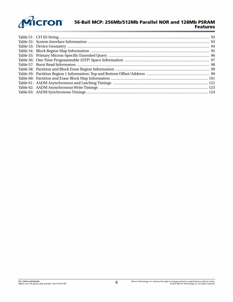
Table 51: CFI ID String ................................................................................................................................... 93Table 52: System Interface Information .......................................................................................................... 93Table 53: Device Geometry ............................................................................................................................ 94Table 54: Block Region Map Information ........................................................................................................ 95Table 55: Primary Micron-Specific Extended Query ........................................................................................ 96Table 56: One Time Programmable (OTP) Space Information .......................................................................... 97Table 57: Burst Read Informaton .................................................................................................................... 98Table 58: Partition and Block Erase Region Information .................................................................................. 99Table 59: Partition Region 1 Information: Top and Bottom Offset/Address ....................................................... 99Table 60: Partition and Erase Block Map Information ..................................................................................... 101Table 61: AADM Asynchronous and Latching Timings ................................................................................... 121Table 62: AADM Asynchronous Write Timings ............................................................................................... 123Table 63: AADM Synchronous Timings .......................................................................................................... 124
56-Ball MCP: 256Mb/512Mb Parallel NOR and 128Mb PSRAMFeatures
PDF: 09005aef86484a8856ball_nor-m18_psram_jxk6_jxr6.pdf - Rev. B 07/15 EN 6 Micron Technology, Inc. reserves the right to change products or specifications without notice.
© 2015 Micron Technology, Inc. All rights reserved.
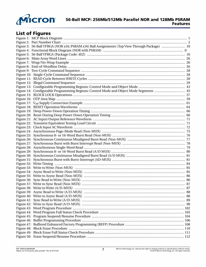
List of FiguresFigure 1: MCP Block Diagram .......................................................................................................................... 1Figure 2: Part Number Chart ............................................................................................................................ 2Figure 3: 56-Ball TFBGA (NOR x16; PSRAM x16) Ball Assignments (Top View Through Package) ....................... 10Figure 4: Functional Block Diagram (NOR with PSRAM) ............................................................................... 0Figure 5: 56-Ball VFBGA (Package Code: 4EZ) ................................................................................................. 16Figure 6: Main Array Word Lines .................................................................................................................... 26Figure 7: Wrap/No-Wrap Example ................................................................................................................. 26Figure 8: End-of-Wordline Delay .................................................................................................................... 26Figure 9: Two-Cycle Command Sequence ....................................................................................................... 28Figure 10: Single-Cycle Command Sequence .................................................................................................. 28Figure 11: READ Cycle Between WRITE Cycles ................................................................................................ 28Figure 12: Illegal Command Sequence ........................................................................................................... 29Figure 13: Configurable Programming Regions: Control Mode and Object Mode .............................................. 43Figure 14: Configurable Programming Regions: Control Mode and Object Mode Segments .............................. 45Figure 15: BLOCK LOCK Operations ............................................................................................................... 57Figure 16: OTP Area Map ............................................................................................................................... 59Figure 17: VPP Supply Connection Example .................................................................................................... 61Figure 18: RESET Operation Waveforms ......................................................................................................... 64Figure 19: Deep Power-Down Operation Timing ............................................................................................. 66Figure 20: Reset During Deep Power-Down Operation Timing ......................................................................... 66Figure 21: AC Input/Output Reference Waveform ........................................................................................... 71Figure 22: Transient Equivalent Testing Load Circuit ....................................................................................... 71Figure 23: Clock Input AC Waveform .............................................................................................................. 72Figure 24: Asynchronous Page-Mode Read (Non-MUX) .................................................................................. 75Figure 25: Synchronous 8- or 16-Word Burst Read (Non-MUX) ........................................................................ 76Figure 26: Synchronous Continuous Misaligned Burst Read (Non-MUX) ......................................................... 77Figure 27: Synchronous Burst with Burst Interrupt Read (Non-MUX) .............................................................. 78Figure 28: Asynchronous Single-Word Read .................................................................................................... 79Figure 29: Synchronous 8- or 16-Word Burst Read (A/D MUX) ......................................................................... 80Figure 30: Synchronous Continuous Misaligned Burst Read (A/D MUX) .......................................................... 81Figure 31: Synchronous Burst with Burst-Interrupt (AD-MUX) ........................................................................ 81Figure 32: Write Timing ................................................................................................................................. 84Figure 33: Write to Write (Non-MUX) ............................................................................................................. 85Figure 34: Async Read to Write (Non-MUX) .................................................................................................... 85Figure 35: Write to Async Read (Non-MUX) .................................................................................................... 86Figure 36: Sync Read to Write (Non-MUX) ...................................................................................................... 86Figure 37: Write to Sync Read (Non-MUX) ...................................................................................................... 87Figure 38: Write to Write (A/D-MUX) ............................................................................................................. 87Figure 39: Async Read to Write (A/D-MUX) .................................................................................................... 88Figure 40: Write to Async Read (A/D-MUX) .................................................................................................... 88Figure 41: Sync Read to Write (A/D-MUX) ...................................................................................................... 89Figure 42: Write to Sync Read (A/D-MUX) ...................................................................................................... 90Figure 43: Word Program Procedure .............................................................................................................. 102Figure 44: Word Program Full Status Check Procedure ................................................................................... 103Figure 45: Program Suspend/Resume Procedure ........................................................................................... 104Figure 46: Buffer Programming Procedure ..................................................................................................... 106Figure 47: Buffered Enhanced Factory Programming (BEFP) Procedure .......................................................... 108Figure 48: Block Erase Procedure .................................................................................................................. 110Figure 49: Block Erase Full Status Check Procedure ........................................................................................ 111Figure 50: Erase Suspend/Resume Procedure ................................................................................................ 112
56-Ball MCP: 256Mb/512Mb Parallel NOR and 128Mb PSRAMFeatures
PDF: 09005aef86484a8856ball_nor-m18_psram_jxk6_jxr6.pdf - Rev. B 07/15 EN 7 Micron Technology, Inc. reserves the right to change products or specifications without notice.
© 2015 Micron Technology, Inc. All rights reserved.
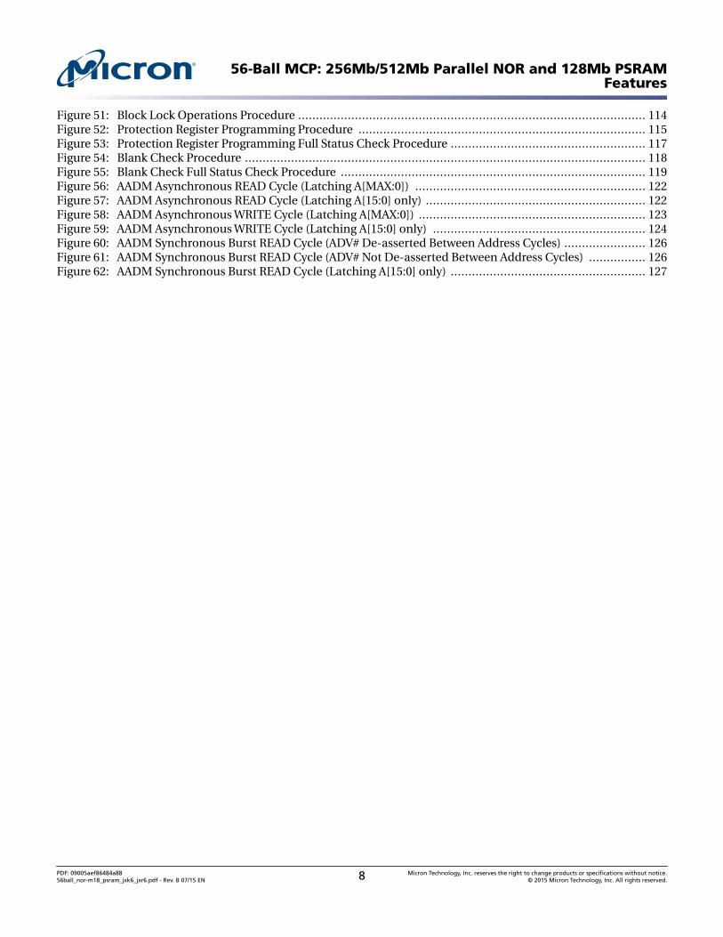
Figure 51: Block Lock Operations Procedure .................................................................................................. 114Figure 52: Protection Register Programming Procedure ................................................................................. 115Figure 53: Protection Register Programming Full Status Check Procedure ....................................................... 117Figure 54: Blank Check Procedure ................................................................................................................. 118Figure 55: Blank Check Full Status Check Procedure ...................................................................................... 119Figure 56: AADM Asynchronous READ Cycle (Latching A[MAX:0]) ................................................................. 122Figure 57: AADM Asynchronous READ Cycle (Latching A[15:0] only) .............................................................. 122Figure 58: AADM Asynchronous WRITE Cycle (Latching A[MAX:0]) ................................................................ 123Figure 59: AADM Asynchronous WRITE Cycle (Latching A[15:0] only) ............................................................ 124Figure 60: AADM Synchronous Burst READ Cycle (ADV# De-asserted Between Address Cycles) ....................... 126Figure 61: AADM Synchronous Burst READ Cycle (ADV# Not De-asserted Between Address Cycles) ................ 126Figure 62: AADM Synchronous Burst READ Cycle (Latching A[15:0] only) ....................................................... 127
56-Ball MCP: 256Mb/512Mb Parallel NOR and 128Mb PSRAMFeatures
PDF: 09005aef86484a8856ball_nor-m18_psram_jxk6_jxr6.pdf - Rev. B 07/15 EN 8 Micron Technology, Inc. reserves the right to change products or specifications without notice.
© 2015 Micron Technology, Inc. All rights reserved.
MCP General DescriptionMicron MCP products combine NOR Flash and PSRAM devices in a single MCP.
Recommended operating conditions do not allow more than one device to be active at atime. A common example of this scenario is running simultaneous READ operations onthe NOR device and on the PSRAM device. Doing this results in data bus contention. Toprevent this, one device must be High-Z when reading the selected device.
The PSRAM ADM device is W957D6H. For device specifications and complete PSRAMfeatures documentation, contact your local Micron sales office.
56-Ball MCP: 256Mb/512Mb Parallel NOR and 128Mb PSRAMMCP General Description
PDF: 09005aef86484a8856ball_nor-m18_psram_jxk6_jxr6.pdf - Rev. B 07/15 EN 9 Micron Technology, Inc. reserves the right to change products or specifications without notice.
© 2015 Micron Technology, Inc. All rights reserved.
Ball Assignments and Descriptions
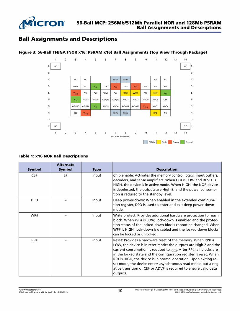
Figure 3: 56-Ball TFBGA (NOR x16; PSRAM x16) Ball Assignments (Top View Through Package)
Top View (ball down)
GroundSupplyFlashPSRAM
A
B
C
D
E
F
G
H
J
K
A
B
C
D
E
F
G
H
J
K
1
NC
NC
1
2
2
3
NC
WAIT
VCCQ
VSS
A/DQ15
NC
3
4
NC
A21
A16
A/DQ7
A/DQ14
VCCQ
4
5
VSS
A20
A/DQ6
VSS
5
6
CLK
ADV#
A/DQ13
A/DQ5
6
7
LB#p
VCC
A23
A/DQ12
A/DQ4
CE#p
7
8
UB#p
WE#
RST#f
A/DQ3
A/DQ11
CREp
8
9
VPPf
WP#f
A/DQ2
A/DQ10
9
10
A19
A18
A/DQ9
VCCQ
10
11
A24
A17
CE#f
A/DQ8
A/DQ1
DPD
11
12
NC
A22
VSS
OE#
A/DQ0
NC
12
13
13
14
NC
NC
14
Table 1: x16 NOR Ball Descriptions
SymbolAlternateSymbol Type Description
CE# E# Input Chip enable: Activates the memory control logics, input buffers,decoders, and sense amplifiers. When CE# is LOW and RESET isHIGH, the device is in active mode. When HIGH, the NOR deviceis deselected, the outputs are High-Z, and the power consump-tion is reduced to the standby level.
DPD – Input Deep power-down: When enabled in the extended configura-tion register, DPD is used to enter and exit deep power-downmode.
WP# – Input Write protect: Provides additional hardware protection for eachblock. When WP# is LOW, lock-down is enabled and the protec-tion status of the locked-down blocks cannot be changed. WhenWP# is HIGH, lock-down is disabled and the locked-down blockscan be locked or unlocked.
RP# – Input Reset: Provides a hardware reset of the memory. When RP# isLOW, the device is in reset mode; the outputs are High-Z and thecurrent consumption is reduced to IDD2. After RP#, all blocks arein the locked state and the configuration register is reset. WhenRP# is HIGH, the device is in normal operation. Upon exiting re-set mode, the device enters asynchronous read mode, but a neg-ative transition of CE# or ADV# is required to ensure valid dataoutputs.
56-Ball MCP: 256Mb/512Mb Parallel NOR and 128Mb PSRAMBall Assignments and Descriptions
PDF: 09005aef86484a8856ball_nor-m18_psram_jxk6_jxr6.pdf - Rev. B 07/15 EN 10 Micron Technology, Inc. reserves the right to change products or specifications without notice.
© 2015 Micron Technology, Inc. All rights reserved.
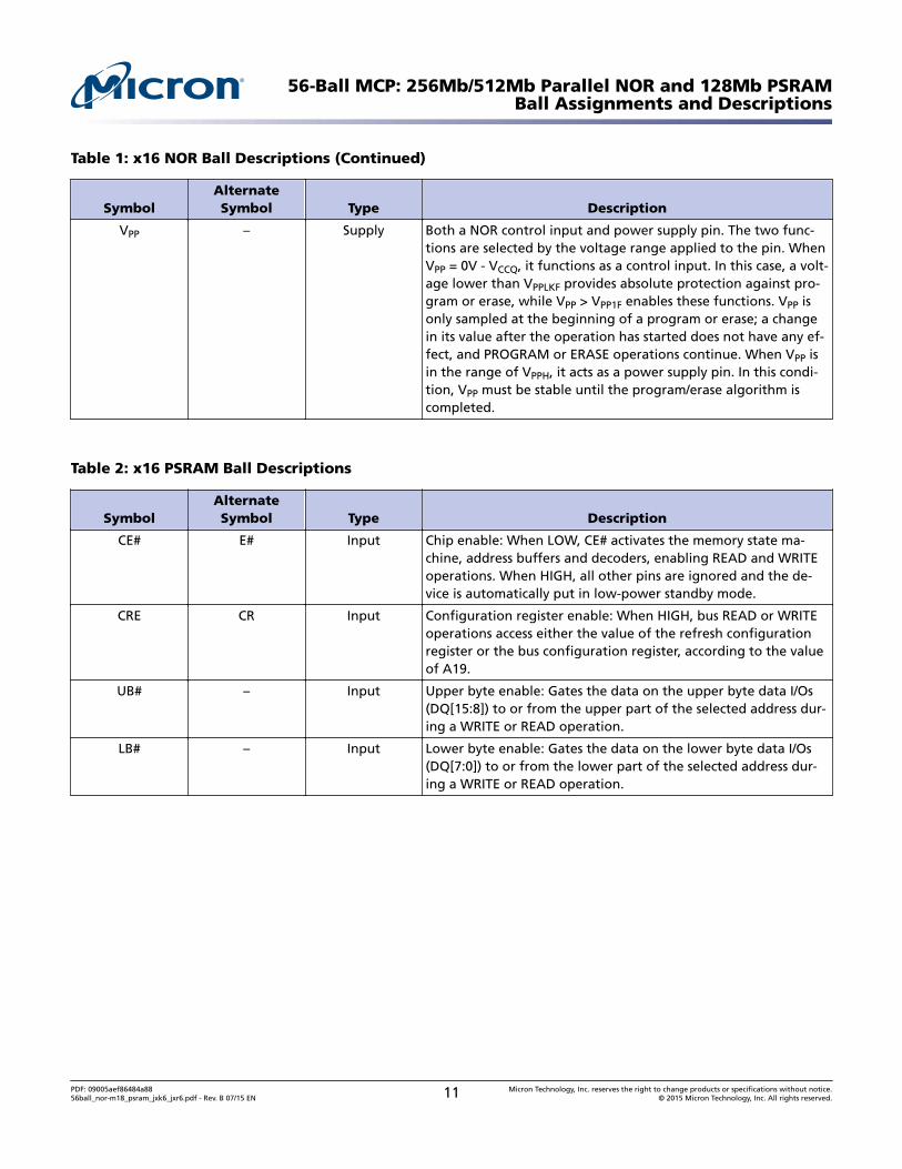
Table 1: x16 NOR Ball Descriptions (Continued)
SymbolAlternateSymbol Type Description
VPP – Supply Both a NOR control input and power supply pin. The two func-tions are selected by the voltage range applied to the pin. WhenVPP = 0V - VCCQ, it functions as a control input. In this case, a volt-age lower than VPPLKF provides absolute protection against pro-gram or erase, while VPP > VPP1F enables these functions. VPP isonly sampled at the beginning of a program or erase; a changein its value after the operation has started does not have any ef-fect, and PROGRAM or ERASE operations continue. When VPP isin the range of VPPH, it acts as a power supply pin. In this condi-tion, VPP must be stable until the program/erase algorithm iscompleted.
Table 2: x16 PSRAM Ball Descriptions
SymbolAlternateSymbol Type Description
CE# E# Input Chip enable: When LOW, CE# activates the memory state ma-chine, address buffers and decoders, enabling READ and WRITEoperations. When HIGH, all other pins are ignored and the de-vice is automatically put in low-power standby mode.
CRE CR Input Configuration register enable: When HIGH, bus READ or WRITEoperations access either the value of the refresh configurationregister or the bus configuration register, according to the valueof A19.
UB# – Input Upper byte enable: Gates the data on the upper byte data I/Os(DQ[15:8]) to or from the upper part of the selected address dur-ing a WRITE or READ operation.
LB# – Input Lower byte enable: Gates the data on the lower byte data I/Os(DQ[7:0]) to or from the lower part of the selected address dur-ing a WRITE or READ operation.
56-Ball MCP: 256Mb/512Mb Parallel NOR and 128Mb PSRAMBall Assignments and Descriptions
PDF: 09005aef86484a8856ball_nor-m18_psram_jxk6_jxr6.pdf - Rev. B 07/15 EN 11 Micron Technology, Inc. reserves the right to change products or specifications without notice.
© 2015 Micron Technology, Inc. All rights reserved.
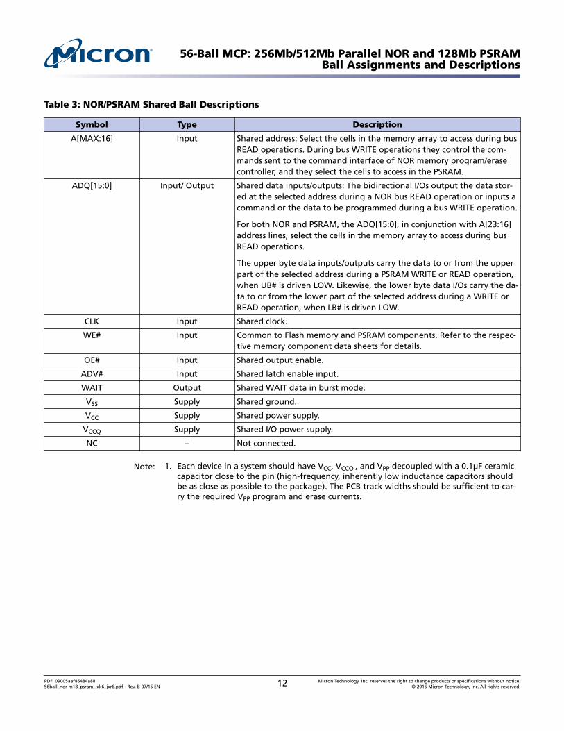
Table 3: NOR/PSRAM Shared Ball Descriptions
Symbol Type Description
A[MAX:16] Input Shared address: Select the cells in the memory array to access during busREAD operations. During bus WRITE operations they control the com-mands sent to the command interface of NOR memory program/erasecontroller, and they select the cells to access in the PSRAM.
ADQ[15:0] Input/ Output Shared data inputs/outputs: The bidirectional I/Os output the data stor-ed at the selected address during a NOR bus READ operation or inputs acommand or the data to be programmed during a bus WRITE operation.
For both NOR and PSRAM, the ADQ[15:0], in conjunction with A[23:16]address lines, select the cells in the memory array to access during busREAD operations.
The upper byte data inputs/outputs carry the data to or from the upperpart of the selected address during a PSRAM WRITE or READ operation,when UB# is driven LOW. Likewise, the lower byte data I/Os carry the da-ta to or from the lower part of the selected address during a WRITE orREAD operation, when LB# is driven LOW.
CLK Input Shared clock.
WE# Input Common to Flash memory and PSRAM components. Refer to the respec-tive memory component data sheets for details.
OE# Input Shared output enable.
ADV# Input Shared latch enable input.
WAIT Output Shared WAIT data in burst mode.
VSS Supply Shared ground.
VCC Supply Shared power supply.
VCCQ Supply Shared I/O power supply.
NC – Not connected.
Note: 1. Each device in a system should have VCC, VCCQ , and VPP decoupled with a 0.1µF ceramiccapacitor close to the pin (high-frequency, inherently low inductance capacitors shouldbe as close as possible to the package). The PCB track widths should be sufficient to car-ry the required VPP program and erase currents.
56-Ball MCP: 256Mb/512Mb Parallel NOR and 128Mb PSRAMBall Assignments and Descriptions
PDF: 09005aef86484a8856ball_nor-m18_psram_jxk6_jxr6.pdf - Rev. B 07/15 EN 12 Micron Technology, Inc. reserves the right to change products or specifications without notice.
© 2015 Micron Technology, Inc. All rights reserved.
Electrical SpecificationsStresses greater than those listed may cause permanent damage to the device. This is astress rating only, and functional operation of the device at these or any other condi-tions above those indicated in the operational sections of this specification is not im-plied. Exposure to absolute maximum rating conditions for extended periods may affectreliability.
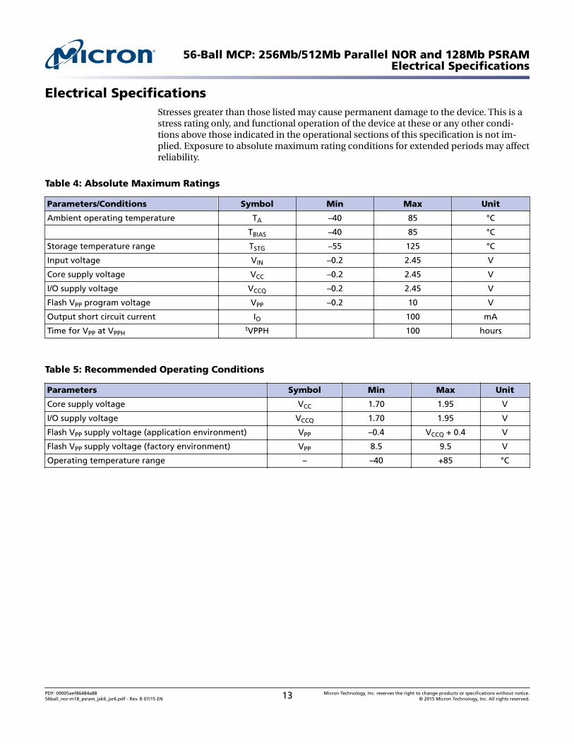
Table 4: Absolute Maximum Ratings
Parameters/Conditions Symbol Min Max Unit
Ambient operating temperature TA –40 85 °C
TBIAS –40 85 °C
Storage temperature range TSTG –55 125 °C
Input voltage VIN –0.2 2.45 V
Core supply voltage VCC –0.2 2.45 V
I/O supply voltage VCCQ –0.2 2.45 V
Flash VPP program voltage VPP –0.2 10 V
Output short circuit current IO 100 mA
Time for VPP at VPPHtVPPH 100 hours
Table 5: Recommended Operating Conditions
Parameters Symbol Min Max Unit
Core supply voltage VCC 1.70 1.95 V
I/O supply voltage VCCQ 1.70 1.95 V
Flash VPP supply voltage (application environment) VPP –0.4 VCCQ + 0.4 V
Flash VPP supply voltage (factory environment) VPP 8.5 9.5 V
Operating temperature range – –40 +85 °C
56-Ball MCP: 256Mb/512Mb Parallel NOR and 128Mb PSRAMElectrical Specifications
PDF: 09005aef86484a8856ball_nor-m18_psram_jxk6_jxr6.pdf - Rev. B 07/15 EN 13 Micron Technology, Inc. reserves the right to change products or specifications without notice.
© 2015 Micron Technology, Inc. All rights reserved.
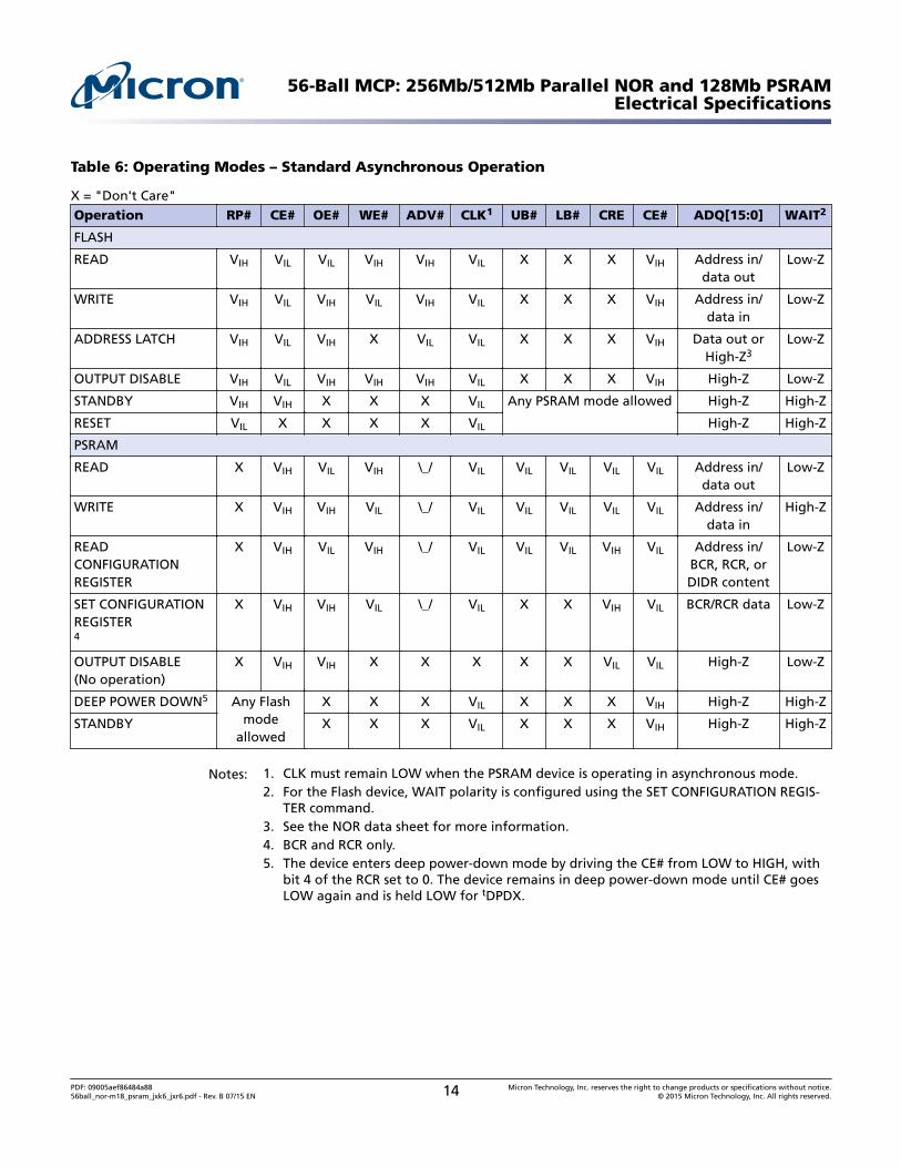
Table 6: Operating Modes – Standard Asynchronous Operation
X = "Don't Care"Operation RP# CE# OE# WE# ADV# CLK1 UB# LB# CRE CE# ADQ[15:0] WAIT2
FLASH
READ VIH VIL VIL VIH VIH VIL X X X VIH Address in/data out
Low-Z
WRITE VIH VIL VIH VIL VIH VIL X X X VIH Address in/data in
Low-Z
ADDRESS LATCH VIH VIL VIH X VIL VIL X X X VIH Data out orHigh-Z3
Low-Z
OUTPUT DISABLE VIH VIL VIH VIH VIH VIL X X X VIH High-Z Low-Z
STANDBY VIH VIH X X X VIL Any PSRAM mode allowed High-Z High-Z
RESET VIL X X X X VIL High-Z High-Z
PSRAM
READ X VIH VIL VIH \_/ VIL VIL VIL VIL VIL Address in/data out
Low-Z
WRITE X VIH VIH VIL \_/ VIL VIL VIL VIL VIL Address in/data in
High-Z
READCONFIGURATIONREGISTER
X VIH VIL VIH \_/ VIL VIL VIL VIH VIL Address in/BCR, RCR, orDIDR content
Low-Z
SET CONFIGURATIONREGISTER4
X VIH VIH VIL \_/ VIL X X VIH VIL BCR/RCR data Low-Z
OUTPUT DISABLE(No operation)
X VIH VIH X X X X X VIL VIL High-Z Low-Z
DEEP POWER DOWN5 Any Flashmode
allowed
X X X VIL X X X VIH High-Z High-Z
STANDBY X X X VIL X X X VIH High-Z High-Z
Notes: 1. CLK must remain LOW when the PSRAM device is operating in asynchronous mode.2. For the Flash device, WAIT polarity is configured using the SET CONFIGURATION REGIS-
TER command.3. See the NOR data sheet for more information.4. BCR and RCR only.5. The device enters deep power-down mode by driving the CE# from LOW to HIGH, with
bit 4 of the RCR set to 0. The device remains in deep power-down mode until CE# goesLOW again and is held LOW for tDPDX.
56-Ball MCP: 256Mb/512Mb Parallel NOR and 128Mb PSRAMElectrical Specifications
PDF: 09005aef86484a8856ball_nor-m18_psram_jxk6_jxr6.pdf - Rev. B 07/15 EN 14 Micron Technology, Inc. reserves the right to change products or specifications without notice.
© 2015 Micron Technology, Inc. All rights reserved.
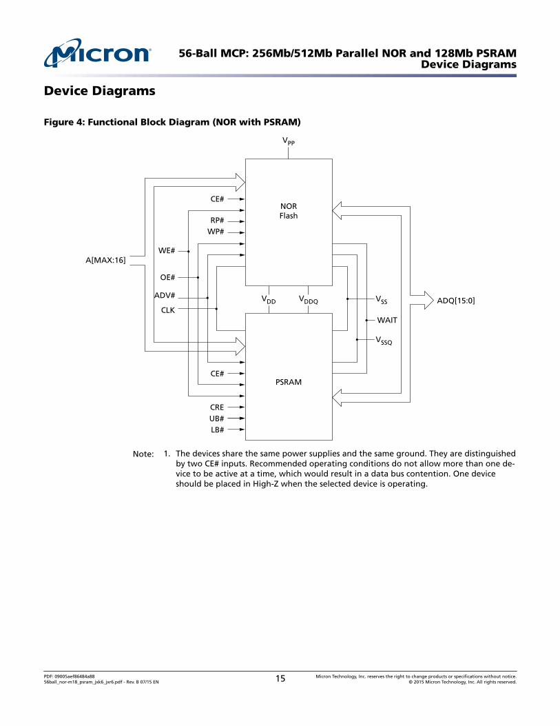
Device Diagrams
Figure 4: Functional Block Diagram (NOR with PSRAM)
A[MAX:16]
ADQ[15:0]
NORFlash
PSRAM
OE#
WE#
CE#
RP#WP#
CLK
ADV#
CE#
CREUB#LB#
WAIT
VSS
VSSQ
VPP
VDDQVDD
Note: 1. The devices share the same power supplies and the same ground. They are distinguishedby two CE# inputs. Recommended operating conditions do not allow more than one de-vice to be active at a time, which would result in a data bus contention. One deviceshould be placed in High-Z when the selected device is operating.
56-Ball MCP: 256Mb/512Mb Parallel NOR and 128Mb PSRAMDevice Diagrams
PDF: 09005aef86484a8856ball_nor-m18_psram_jxk6_jxr6.pdf - Rev. B 07/15 EN 15 Micron Technology, Inc. reserves the right to change products or specifications without notice.
© 2015 Micron Technology, Inc. All rights reserved.
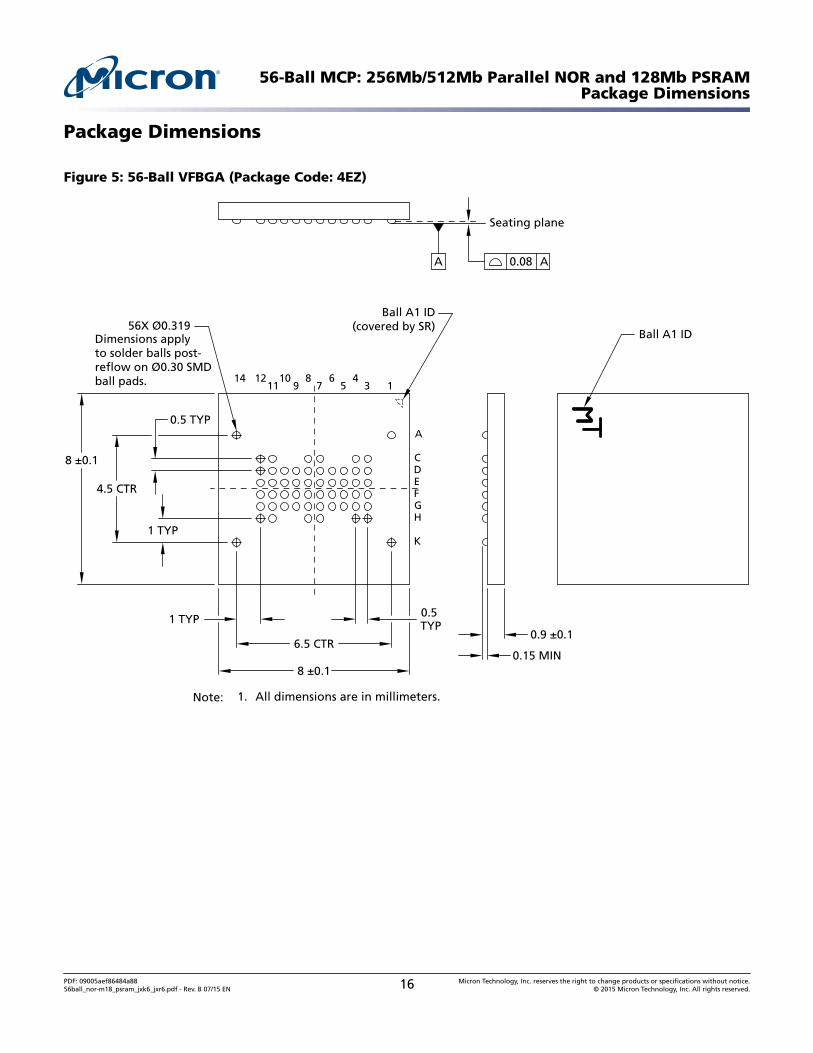
Package Dimensions
Figure 5: 56-Ball VFBGA (Package Code: 4EZ)
Seating plane
1
A
CDEFGH
K
357911468101214
8 ±0.1
4.5 CTR
1 TYP
8 ±0.1
6.5 CTR
1 TYP 0.5TYP
0.5 TYP
0.15 MIN
0.9 ±0.1
56X Ø0.319Dimensions applyto solder balls post-reflow on Ø0.30 SMDball pads.
0.08 AA
Ball A1 ID(covered by SR)
Ball A1 ID
Note: 1. All dimensions are in millimeters.
56-Ball MCP: 256Mb/512Mb Parallel NOR and 128Mb PSRAMPackage Dimensions
PDF: 09005aef86484a8856ball_nor-m18_psram_jxk6_jxr6.pdf - Rev. B 07/15 EN 16 Micron Technology, Inc. reserves the right to change products or specifications without notice.
© 2015 Micron Technology, Inc. All rights reserved.
256Mb, 512Mb, 1Gb StrataFlash® Memory
Features
• High-performance read, program, and erase– 96ns initial read access– 108 MHz with zero wait-state synchronous burst reads: 7ns clock-to-data output– 133 MHz with zero wait-state synchronous burst reads: 5.5ns clock-to-data output– 8-, 16-, and continuous-word synchronous-burst reads– Programmable WAIT configuration– Customer-configurable output driver impedance– Buffered programming: 2.0 μs/Word (TYP), 512Mb, 65nm– Block erase: 0.9s per block (TYP)– 20μs (TYP) program/erase suspend
• Architecture– 16-bit wide data bus– Multilevel cell technology– Symmetrically-blocked array architecture– 256KB erase blocks– 1Gb device: Eight 128Mb partitions– 512Mb device: Eight 64Mb partitions– 256Mb device: Eight 32Mb partitions– READ-While-PROGRAM and READ-While-ERASE commands– Status register for partition/device status– Blank check feature
• Temperature Range– Expanded temperature: –40°C to +85°C
• JESD47H-compliant– Minimum 100,000 ERASE cycles per block– Data retention: 20 years (TYP)
56-Ball MCP: 256Mb/512Mb Parallel NOR and 128Mb PSRAM256Mb, 512Mb, 1Gb StrataFlash® Memory
PDF: 09005aef86484a8856ball_nor-m18_psram_jxk6_jxr6.pdf - Rev. B 07/15 EN 17 Micron Technology, Inc. reserves the right to change products or specifications without notice.
© 2015 Micron Technology, Inc. All rights reserved.
• Power– Core voltage: 1.7– 2.0V– I/O voltage: 1.7–2.0V– Standby current: 60μA (TYP) for 512Mb, 65nm– Automatic power savings mode– 16-word synchronous-burst read current: 23mA (TYP) @ 108 MHz; 24mA (TYP) @
133 MHz• Software
– Micron® Flash data integrator (FDI) optimized– Basic command set (BCS) and extended command set (ECS) compatible– Common Flash interface (CFI) capable
• Security– One-time programmable (OTP) space
64 unique factory device identifier bits2112 user-programmable OTP bits
– Absolute write protection: VPP = GND– Power-transition erase/program lockout– Individual zero latency block locking– Individual block lock-down
• Density and packaging– 256Mb, 512Mb, and 1Gb– Address-data multiplexed and non-multiplexed interfaces
General DescriptionMicron's 65nm device is the latest generation of StrataFlash® memory featuring flexible,multiple-partition, dual-operation architecture. The device provides high-performance,asynchronous read mode and synchronous-burst read mode using 1.8V low-voltage,multilevel cell (MLC) technology.
The multiple-partition architecture enables background programming or erasing to oc-cur in one partition while code execution or data reads take place in another partition.This dual-operation architecture also allows two processors to interleave code opera-tions while PROGRAM and ERASE operations take place in the background. The multi-ple partitions allow flexibility for system designers to choose the size of the code anddata segments.
The device is manufactured using 65nm process technologies and is available in indus-try-standard chip scale packaging.
Functional OverviewThis device provides high read and write performance at low voltage on a 16-bit databus. The multi-partition architecture provides read-while-write and read-while-erasecapability, with individually erasable memory blocks sized for optimum code and datastorage.
The device supports synchronous burst reads up to 133 MHz using CLK latching.
Upon initial power-up or return from reset, the device defaults to asynchronous readmode. Configuring the read configuration register enables synchronous burst modereads. In synchronous burst mode, output data is synchronized with a user-supplied
56-Ball MCP: 256Mb/512Mb Parallel NOR and 128Mb PSRAMGeneral Description
PDF: 09005aef86484a8856ball_nor-m18_psram_jxk6_jxr6.pdf - Rev. B 07/15 EN 18 Micron Technology, Inc. reserves the right to change products or specifications without notice.
© 2015 Micron Technology, Inc. All rights reserved.
clock signal. In continuous-burst mode, a data read can traverse partition boundaries. AWAIT signal simplifies synchronizing the CPU to the memory.
Designed for low-voltage applications, the device supports READ operations with VCC at1.8V, and ERASE and PROGRAM operations with VPP at 1.8V or 9.0V. VCC and VPP can betied together for a simple, ultra low-power design. In addition to voltage flexibility, adedicated VPP connection provides complete data protection when VPP is less thanVPPLK.
A status register provides status and error conditions of ERASE and PROGRAM opera-tions.
One-time programmable (OTP) area enables unique identification that can be used toincrease security. Additionally, the individual block lock feature provides zero-latencyblock locking and unlocking to protect against unwanted program or erase of the array.
The device offers power-savings features, including automatic power savings mode,standby mode, and deep power-down mode. For power savings, the device automati-cally enters APS following a READ cycle. Standby is initiated when the system deselectsthe device by de-asserting CE#. Deep power-down mode starts when the device is prop-erly configured (ECR15 is set) and the DPD signal is asserted. In deep power-downmode, the device has the lowest power consumption.
56-Ball MCP: 256Mb/512Mb Parallel NOR and 128Mb PSRAMFunctional Overview
PDF: 09005aef86484a8856ball_nor-m18_psram_jxk6_jxr6.pdf - Rev. B 07/15 EN 19 Micron Technology, Inc. reserves the right to change products or specifications without notice.
© 2015 Micron Technology, Inc. All rights reserved.
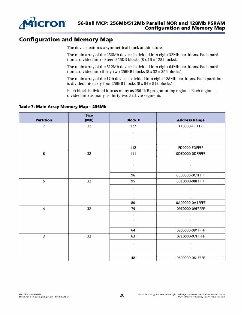
Configuration and Memory MapThe device features a symmetrical block architecture.
The main array of the 256Mb device is divided into eight 32Mb partitions. Each parti-tion is divided into sixteen 256KB blocks (8 x 16 = 128 blocks).
The main array of the 512Mb device is divided into eight 64Mb partitions. Each parti-tion is divided into thirty-two 256KB blocks (8 x 32 = 256 blocks).
The main array of the 1Gb device is divided into eight 128Mb partitions. Each partitionis divided into sixty-four 256KB blocks (8 x 64 = 512 blocks).
Each block is divided into as many as 256 1KB programming regions. Each region isdivided into as many as thirty-two 32-byte segments
Table 7: Main Array Memory Map – 256Mb
PartitionSize(Mb) Block # Address Range
7 32 127 FF0000-FFFFFF
.
.
.
.
.
.
112 FD0000-FDFFFF
6 32 111 0DE0000-0DFFFFF
.
.
.
.
.
.
96 0C00000-0C1FFFF
5 32 95 0BE0000-0BFFFFF
.
.
.
.
.
.
80 0A00000-0A1FFFF
4 32 79 09E0000-09FFFFF
.
.
.
.
.
.
64 0800000-081FFFF
3 32 63 07E0000-07FFFFF
.
.
.
.
.
.
48 0600000-061FFFF
56-Ball MCP: 256Mb/512Mb Parallel NOR and 128Mb PSRAMConfiguration and Memory Map
PDF: 09005aef86484a8856ball_nor-m18_psram_jxk6_jxr6.pdf - Rev. B 07/15 EN 20 Micron Technology, Inc. reserves the right to change products or specifications without notice.
© 2015 Micron Technology, Inc. All rights reserved.
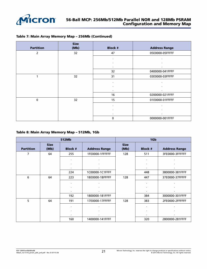
Table 7: Main Array Memory Map – 256Mb (Continued)
PartitionSize(Mb) Block # Address Range
2 32 47 05E0000-05FFFFF
.
.
.
.
.
.
32 0400000-041FFFF
1 32 31 03E0000-03FFFFF
.
.
.
.
.
.
16 0200000-021FFFF
0 32 15 01E0000-01FFFFF
.
.
.
.
.
.
0 0000000-001FFFF
Table 8: Main Array Memory Map – 512Mb, 1Gb
512Mb 1Gb
PartitionSize(Mb) Block # Address Range
Size(Mb) Block # Address Range
7 64 255 1FE0000-1FFFFFF 128 511 3FE0000-3FFFFFF
.
.
.
.
.
.
.
.
.
.
.
.
224 1C00000-1C1FFFF 448 3800000-381FFFF
6 64 223 1BE0000-1BFFFFF 128 447 37E0000-37FFFFF
.
.
.
.
.
.
.
.
.
.
.
.
192 1800000-181FFFF 384 3000000-301FFFF
5 64 191 17E0000-17FFFFF 128 383 2FE0000-2FFFFFF
.
.
.
.
.
.
.
.
.
.
.
.
160 1400000-141FFFF 320 2800000-281FFFF
56-Ball MCP: 256Mb/512Mb Parallel NOR and 128Mb PSRAMConfiguration and Memory Map
PDF: 09005aef86484a8856ball_nor-m18_psram_jxk6_jxr6.pdf - Rev. B 07/15 EN 21 Micron Technology, Inc. reserves the right to change products or specifications without notice.
© 2015 Micron Technology, Inc. All rights reserved.
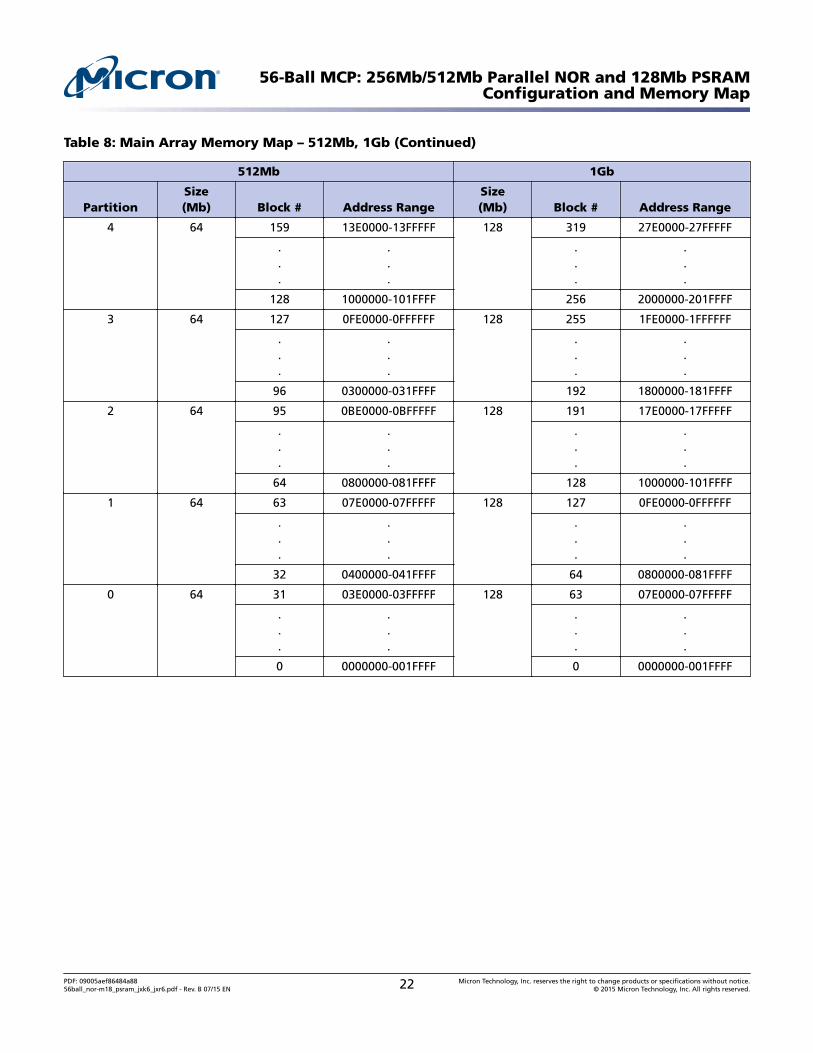
Table 8: Main Array Memory Map – 512Mb, 1Gb (Continued)
512Mb 1Gb
PartitionSize(Mb) Block # Address Range
Size(Mb) Block # Address Range
4 64 159 13E0000-13FFFFF 128 319 27E0000-27FFFFF
.
.
.
.
.
.
.
.
.
.
.
.
128 1000000-101FFFF 256 2000000-201FFFF
3 64 127 0FE0000-0FFFFFF 128 255 1FE0000-1FFFFFF
.
.
.
.
.
.
.
.
.
.
.
.
96 0300000-031FFFF 192 1800000-181FFFF
2 64 95 0BE0000-0BFFFFF 128 191 17E0000-17FFFFF
.
.
.
.
.
.
.
.
.
.
.
.
64 0800000-081FFFF 128 1000000-101FFFF
1 64 63 07E0000-07FFFFF 128 127 0FE0000-0FFFFFF
.
.
.
.
.
.
.
.
.
.
.
.
32 0400000-041FFFF 64 0800000-081FFFF
0 64 31 03E0000-03FFFFF 128 63 07E0000-07FFFFF
.
.
.
.
.
.
.
.
.
.
.
.
0 0000000-001FFFF 0 0000000-001FFFF
56-Ball MCP: 256Mb/512Mb Parallel NOR and 128Mb PSRAMConfiguration and Memory Map
PDF: 09005aef86484a8856ball_nor-m18_psram_jxk6_jxr6.pdf - Rev. B 07/15 EN 22 Micron Technology, Inc. reserves the right to change products or specifications without notice.
© 2015 Micron Technology, Inc. All rights reserved.
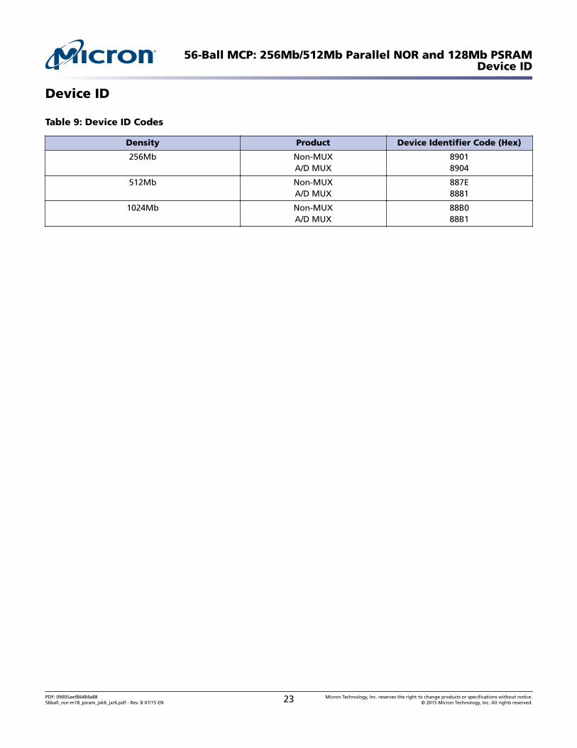
Device ID
Table 9: Device ID Codes
Density Product Device Identifier Code (Hex)
256Mb Non-MUXA/D MUX
89018904
512Mb Non-MUXA/D MUX
887E8881
1024Mb Non-MUXA/D MUX
88B088B1
56-Ball MCP: 256Mb/512Mb Parallel NOR and 128Mb PSRAMDevice ID
PDF: 09005aef86484a8856ball_nor-m18_psram_jxk6_jxr6.pdf - Rev. B 07/15 EN 23 Micron Technology, Inc. reserves the right to change products or specifications without notice.
© 2015 Micron Technology, Inc. All rights reserved.
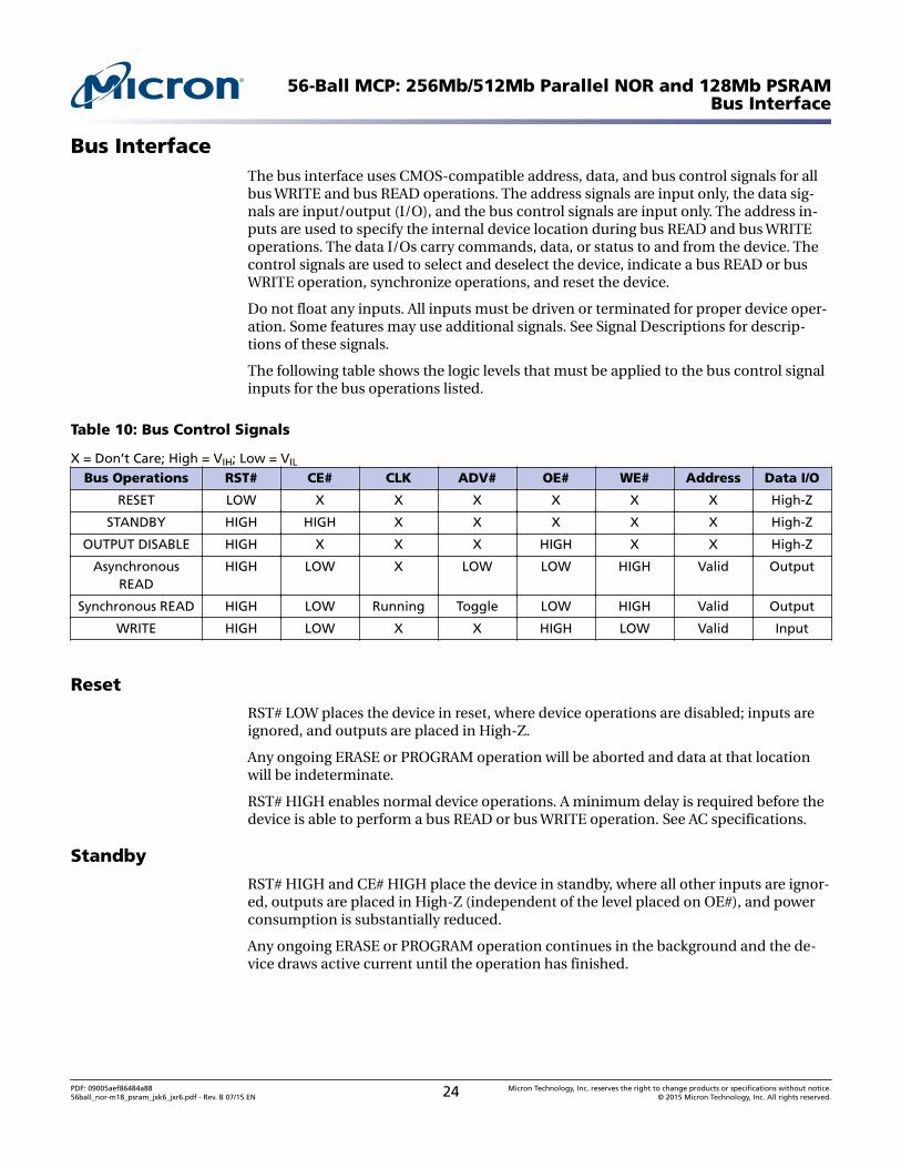
Bus InterfaceThe bus interface uses CMOS-compatible address, data, and bus control signals for allbus WRITE and bus READ operations. The address signals are input only, the data sig-nals are input/output (I/O), and the bus control signals are input only. The address in-puts are used to specify the internal device location during bus READ and bus WRITEoperations. The data I/Os carry commands, data, or status to and from the device. Thecontrol signals are used to select and deselect the device, indicate a bus READ or busWRITE operation, synchronize operations, and reset the device.
Do not float any inputs. All inputs must be driven or terminated for proper device oper-ation. Some features may use additional signals. See Signal Descriptions for descrip-tions of these signals.
The following table shows the logic levels that must be applied to the bus control signalinputs for the bus operations listed.
Table 10: Bus Control Signals
X = Don’t Care; High = VIH; Low = VIL
Bus Operations RST# CE# CLK ADV# OE# WE# Address Data I/O
RESET LOW X X X X X X High-Z
STANDBY HIGH HIGH X X X X X High-Z
OUTPUT DISABLE HIGH X X X HIGH X X High-Z
AsynchronousREAD
HIGH LOW X LOW LOW HIGH Valid Output
Synchronous READ HIGH LOW Running Toggle LOW HIGH Valid Output
WRITE HIGH LOW X X HIGH LOW Valid Input
Reset
RST# LOW places the device in reset, where device operations are disabled; inputs areignored, and outputs are placed in High-Z.
Any ongoing ERASE or PROGRAM operation will be aborted and data at that locationwill be indeterminate.
RST# HIGH enables normal device operations. A minimum delay is required before thedevice is able to perform a bus READ or bus WRITE operation. See AC specifications.
Standby
RST# HIGH and CE# HIGH place the device in standby, where all other inputs are ignor-ed, outputs are placed in High-Z (independent of the level placed on OE#), and powerconsumption is substantially reduced.
Any ongoing ERASE or PROGRAM operation continues in the background and the de-vice draws active current until the operation has finished.
56-Ball MCP: 256Mb/512Mb Parallel NOR and 128Mb PSRAMBus Interface
PDF: 09005aef86484a8856ball_nor-m18_psram_jxk6_jxr6.pdf - Rev. B 07/15 EN 24 Micron Technology, Inc. reserves the right to change products or specifications without notice.
© 2015 Micron Technology, Inc. All rights reserved.
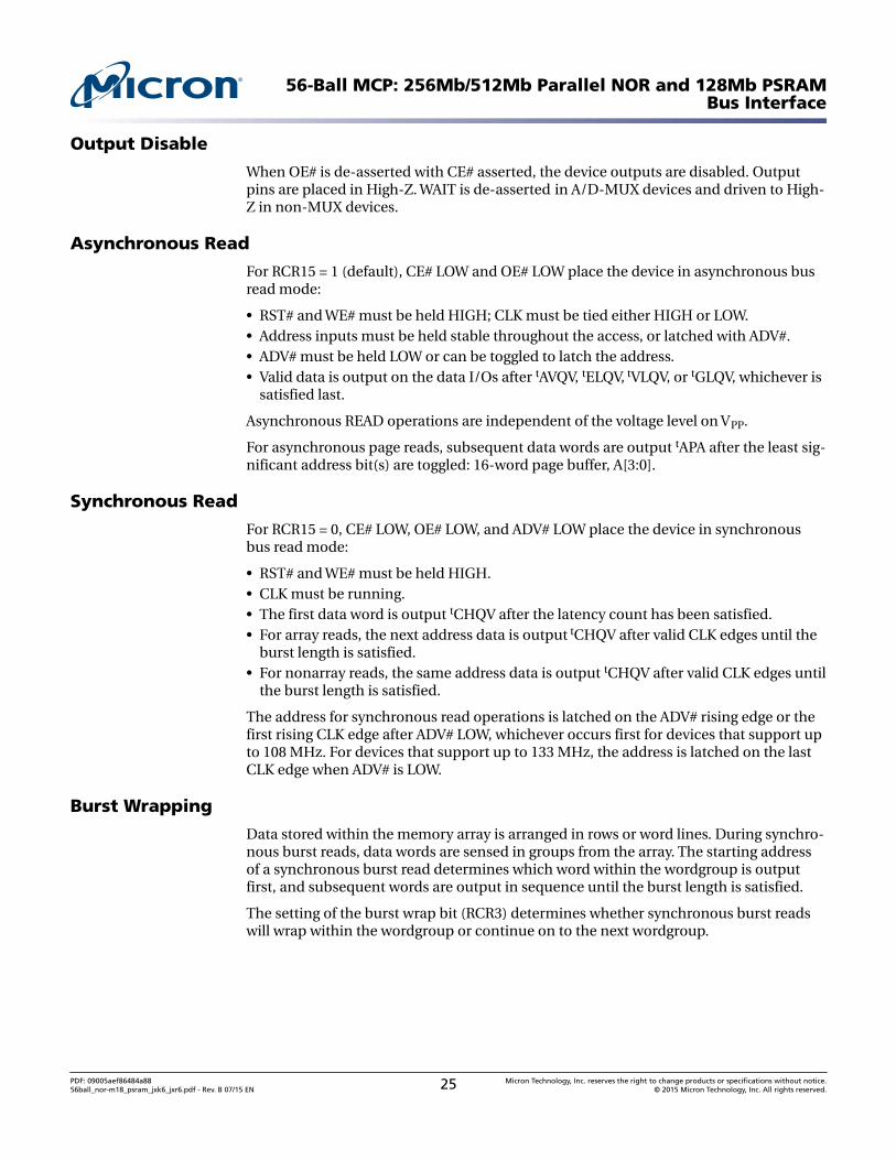
Output Disable
When OE# is de-asserted with CE# asserted, the device outputs are disabled. Outputpins are placed in High-Z. WAIT is de-asserted in A/D-MUX devices and driven to High-Z in non-MUX devices.
Asynchronous Read
For RCR15 = 1 (default), CE# LOW and OE# LOW place the device in asynchronous busread mode:
• RST# and WE# must be held HIGH; CLK must be tied either HIGH or LOW.• Address inputs must be held stable throughout the access, or latched with ADV#.• ADV# must be held LOW or can be toggled to latch the address.• Valid data is output on the data I/Os after tAVQV, tELQV, tVLQV, or tGLQV, whichever is
satisfied last.
Asynchronous READ operations are independent of the voltage level on VPP.
For asynchronous page reads, subsequent data words are output tAPA after the least sig-nificant address bit(s) are toggled: 16-word page buffer, A[3:0].
Synchronous Read
For RCR15 = 0, CE# LOW, OE# LOW, and ADV# LOW place the device in synchronousbus read mode:
• RST# and WE# must be held HIGH.• CLK must be running.• The first data word is output tCHQV after the latency count has been satisfied.• For array reads, the next address data is output tCHQV after valid CLK edges until the
burst length is satisfied.• For nonarray reads, the same address data is output tCHQV after valid CLK edges until
the burst length is satisfied.
The address for synchronous read operations is latched on the ADV# rising edge or thefirst rising CLK edge after ADV# LOW, whichever occurs first for devices that support upto 108 MHz. For devices that support up to 133 MHz, the address is latched on the lastCLK edge when ADV# is LOW.
Burst Wrapping
Data stored within the memory array is arranged in rows or word lines. During synchro-nous burst reads, data words are sensed in groups from the array. The starting addressof a synchronous burst read determines which word within the wordgroup is outputfirst, and subsequent words are output in sequence until the burst length is satisfied.
The setting of the burst wrap bit (RCR3) determines whether synchronous burst readswill wrap within the wordgroup or continue on to the next wordgroup.
56-Ball MCP: 256Mb/512Mb Parallel NOR and 128Mb PSRAMBus Interface
PDF: 09005aef86484a8856ball_nor-m18_psram_jxk6_jxr6.pdf - Rev. B 07/15 EN 25 Micron Technology, Inc. reserves the right to change products or specifications without notice.
© 2015 Micron Technology, Inc. All rights reserved.
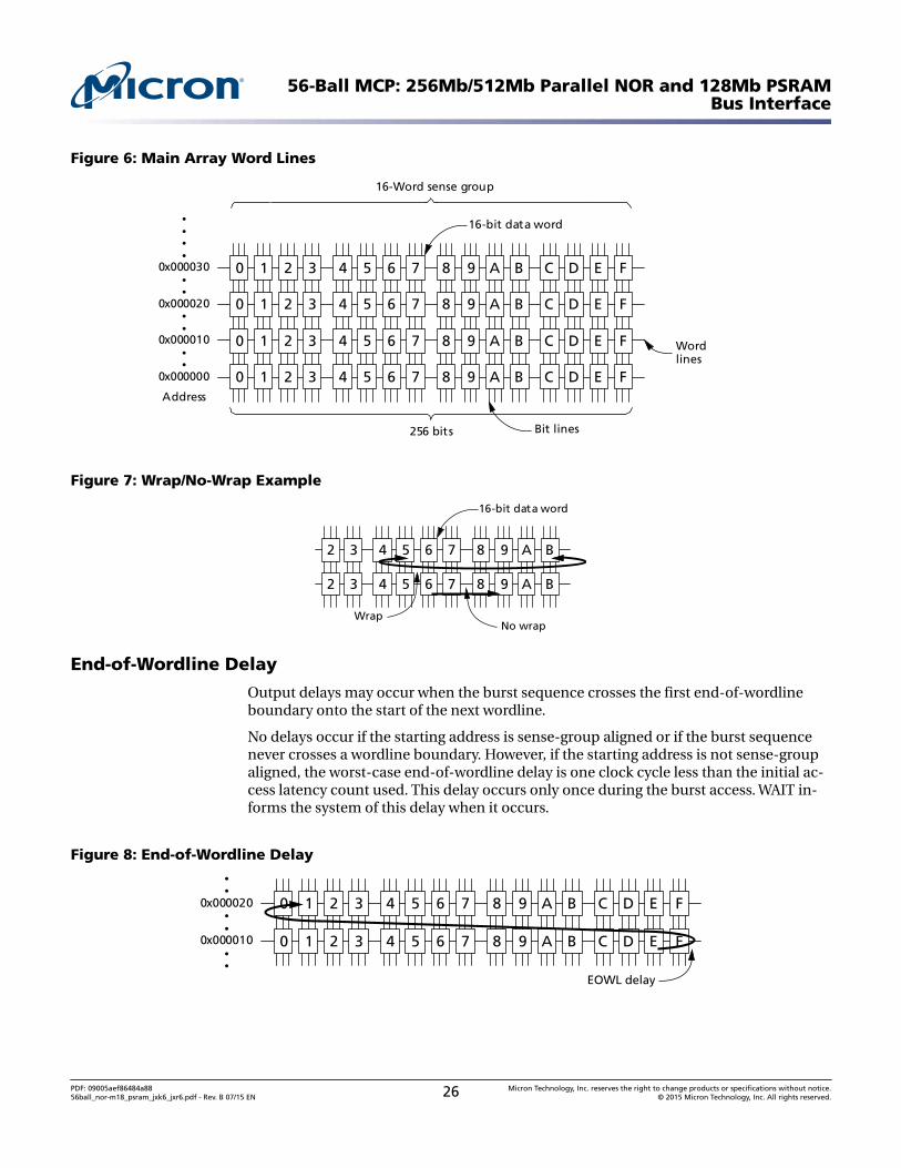
Figure 6: Main Array Word Lines
0 1 2 3 4 5 6 7 8 9 A B C D E F
0 1 2 3 4 5 6 7 8 9 A B C D E F
256 bits
0 1 2 3 4 5 6 7 8 9 A B C D E F
0 1 2 3 4 5 6 7 8 9 A B C D E F
16-bit data word
0x000000
0x000010
0x000020
0x000030
Bit lines
Wordlines
16-Word sense group
Address
Figure 7: Wrap/No-Wrap Example
2 3 4 5 6 7 8 9 A B
2 3 4 5 6 7 8 9 A B
16-bit data word
No wrapWrap
End-of-Wordline Delay
Output delays may occur when the burst sequence crosses the first end-of-wordlineboundary onto the start of the next wordline.
No delays occur if the starting address is sense-group aligned or if the burst sequencenever crosses a wordline boundary. However, if the starting address is not sense-groupaligned, the worst-case end-of-wordline delay is one clock cycle less than the initial ac-cess latency count used. This delay occurs only once during the burst access. WAIT in-forms the system of this delay when it occurs.
Figure 8: End-of-Wordline Delay
0 1 2 3 4 5 6 7 8 9 A B C D E F
0 1 2 3 4 5 6 7 8 9 A B C D E F
0x000010
0x000020
EOWL delay
56-Ball MCP: 256Mb/512Mb Parallel NOR and 128Mb PSRAMBus Interface
PDF: 09005aef86484a8856ball_nor-m18_psram_jxk6_jxr6.pdf - Rev. B 07/15 EN 26 Micron Technology, Inc. reserves the right to change products or specifications without notice.
© 2015 Micron Technology, Inc. All rights reserved.
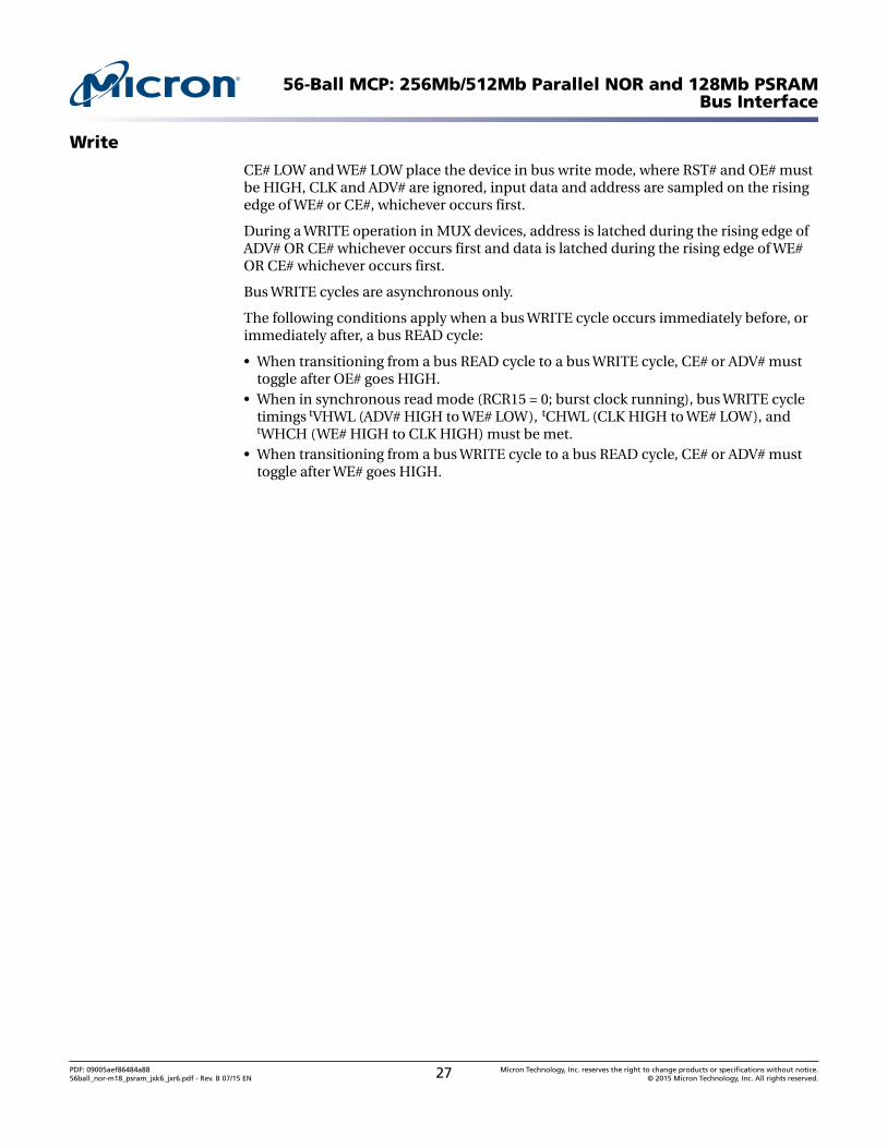
Write
CE# LOW and WE# LOW place the device in bus write mode, where RST# and OE# mustbe HIGH, CLK and ADV# are ignored, input data and address are sampled on the risingedge of WE# or CE#, whichever occurs first.
During a WRITE operation in MUX devices, address is latched during the rising edge ofADV# OR CE# whichever occurs first and data is latched during the rising edge of WE#OR CE# whichever occurs first.
Bus WRITE cycles are asynchronous only.
The following conditions apply when a bus WRITE cycle occurs immediately before, orimmediately after, a bus READ cycle:
• When transitioning from a bus READ cycle to a bus WRITE cycle, CE# or ADV# musttoggle after OE# goes HIGH.
• When in synchronous read mode (RCR15 = 0; burst clock running), bus WRITE cycletimings tVHWL (ADV# HIGH to WE# LOW), tCHWL (CLK HIGH to WE# LOW), andtWHCH (WE# HIGH to CLK HIGH) must be met.
• When transitioning from a bus WRITE cycle to a bus READ cycle, CE# or ADV# musttoggle after WE# goes HIGH.
56-Ball MCP: 256Mb/512Mb Parallel NOR and 128Mb PSRAMBus Interface
PDF: 09005aef86484a8856ball_nor-m18_psram_jxk6_jxr6.pdf - Rev. B 07/15 EN 27 Micron Technology, Inc. reserves the right to change products or specifications without notice.
© 2015 Micron Technology, Inc. All rights reserved.
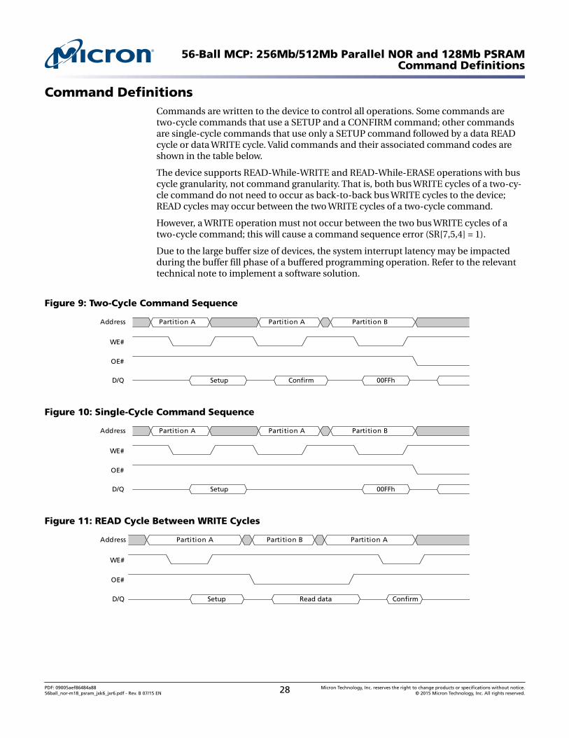
Command DefinitionsCommands are written to the device to control all operations. Some commands aretwo-cycle commands that use a SETUP and a CONFIRM command; other commandsare single-cycle commands that use only a SETUP command followed by a data READcycle or data WRITE cycle. Valid commands and their associated command codes areshown in the table below.
The device supports READ-While-WRITE and READ-While-ERASE operations with buscycle granularity, not command granularity. That is, both bus WRITE cycles of a two-cy-cle command do not need to occur as back-to-back bus WRITE cycles to the device;READ cycles may occur between the two WRITE cycles of a two-cycle command.
However, a WRITE operation must not occur between the two bus WRITE cycles of atwo-cycle command; this will cause a command sequence error (SR[7,5,4] = 1).
Due to the large buffer size of devices, the system interrupt latency may be impactedduring the buffer fill phase of a buffered programming operation. Refer to the relevanttechnical note to implement a software solution.
Figure 9: Two-Cycle Command Sequence
Partition A Partition A Partition B
Setup Confirm 00FFh
Address
WE#
OE#
D/Q
Figure 10: Single-Cycle Command Sequence
Partition A Partition A Partition B
Setup 00FFh
Address
WE#
OE#
D/Q
Figure 11: READ Cycle Between WRITE Cycles
Partition A Partition B Partition A
Setup Confirm
Address
WE#
OE#
D/Q Read data
56-Ball MCP: 256Mb/512Mb Parallel NOR and 128Mb PSRAMCommand Definitions
PDF: 09005aef86484a8856ball_nor-m18_psram_jxk6_jxr6.pdf - Rev. B 07/15 EN 28 Micron Technology, Inc. reserves the right to change products or specifications without notice.
© 2015 Micron Technology, Inc. All rights reserved.
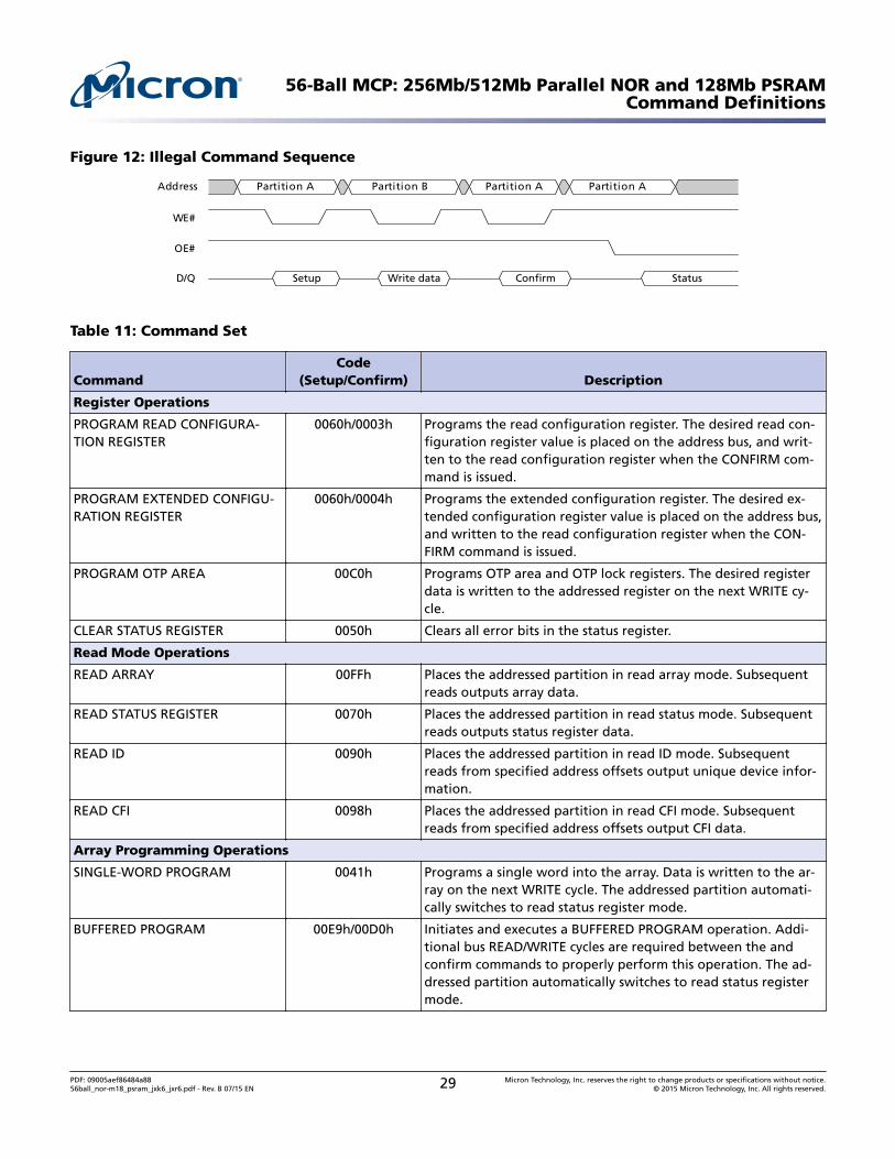
Figure 12: Illegal Command Sequence
Partition A Partition APartition APartition B
Setup Confirm
Address
WE#
OE#
D/Q Write data Status
Table 11: Command Set
CommandCode
(Setup/Confirm) Description
Register Operations
PROGRAM READ CONFIGURA-TION REGISTER
0060h/0003h Programs the read configuration register. The desired read con-figuration register value is placed on the address bus, and writ-ten to the read configuration register when the CONFIRM com-mand is issued.
PROGRAM EXTENDED CONFIGU-RATION REGISTER
0060h/0004h Programs the extended configuration register. The desired ex-tended configuration register value is placed on the address bus,and written to the read configuration register when the CON-FIRM command is issued.
PROGRAM OTP AREA 00C0h Programs OTP area and OTP lock registers. The desired registerdata is written to the addressed register on the next WRITE cy-cle.
CLEAR STATUS REGISTER 0050h Clears all error bits in the status register.
Read Mode Operations
READ ARRAY 00FFh Places the addressed partition in read array mode. Subsequentreads outputs array data.
READ STATUS REGISTER 0070h Places the addressed partition in read status mode. Subsequentreads outputs status register data.
READ ID 0090h Places the addressed partition in read ID mode. Subsequentreads from specified address offsets output unique device infor-mation.
READ CFI 0098h Places the addressed partition in read CFI mode. Subsequentreads from specified address offsets output CFI data.
Array Programming Operations
SINGLE-WORD PROGRAM 0041h Programs a single word into the array. Data is written to the ar-ray on the next WRITE cycle. The addressed partition automati-cally switches to read status register mode.
BUFFERED PROGRAM 00E9h/00D0h Initiates and executes a BUFFERED PROGRAM operation. Addi-tional bus READ/WRITE cycles are required between the andconfirm commands to properly perform this operation. The ad-dressed partition automatically switches to read status registermode.
56-Ball MCP: 256Mb/512Mb Parallel NOR and 128Mb PSRAMCommand Definitions
PDF: 09005aef86484a8856ball_nor-m18_psram_jxk6_jxr6.pdf - Rev. B 07/15 EN 29 Micron Technology, Inc. reserves the right to change products or specifications without notice.
© 2015 Micron Technology, Inc. All rights reserved.
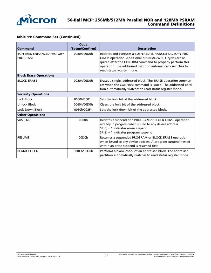
Table 11: Command Set (Continued)
CommandCode
(Setup/Confirm) Description
BUFFERED ENHANCED FACTORYPROGRAM
0080h/00D0h Initiates and executes a BUFFERED ENHANCED FACTORY PRO-GRAM operation. Additional bus READ/WRITE cycles are re-quired after the CONFIRM command to properly perform thisoperation. The addressed partition automatically switches toread status register mode.
Block Erase Operations
BLOCK ERASE 0020h/00D0h Erases a single, addressed block. The ERASE operation commen-ces when the CONFIRM command is issued. The addressed parti-tion automatically switches to read status register mode.
Security Operations
Lock Block 0060h/0001h Sets the lock bit of the addressed block.
Unlock Block 0060h/00D0h Clears the lock bit of the addressed block.
Lock-Down Block 0060h/002Fh Sets the lock-down bit of the addressed block.
Other Operations
SUSPEND 00B0h Initiates a suspend of a PROGRAM or BLOCK ERASE operationalready in progress when issued to any device addressSR[6] = 1 indicates erase suspendSR[2] = 1 indicates program suspend
RESUME 00D0h Resumes a suspended PROGRAM or BLOCK ERASE operationwhen issued to any device address. A program suspend nestedwithin an erase suspend is resumed first.
BLANK CHECK 00BCh/00D0h Performs a blank check of an addressed block. The addressedpartition automatically switches to read status register mode.
56-Ball MCP: 256Mb/512Mb Parallel NOR and 128Mb PSRAMCommand Definitions
PDF: 09005aef86484a8856ball_nor-m18_psram_jxk6_jxr6.pdf - Rev. B 07/15 EN 30 Micron Technology, Inc. reserves the right to change products or specifications without notice.
© 2015 Micron Technology, Inc. All rights reserved.
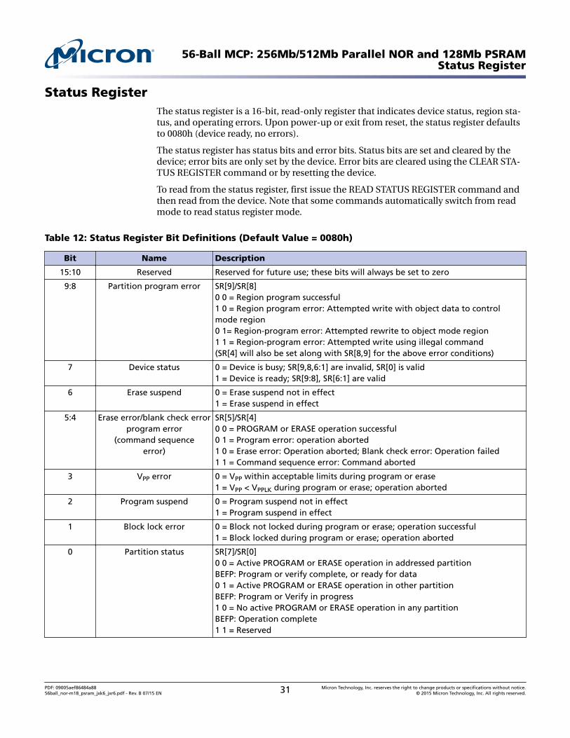
Status RegisterThe status register is a 16-bit, read-only register that indicates device status, region sta-tus, and operating errors. Upon power-up or exit from reset, the status register defaultsto 0080h (device ready, no errors).
The status register has status bits and error bits. Status bits are set and cleared by thedevice; error bits are only set by the device. Error bits are cleared using the CLEAR STA-TUS REGISTER command or by resetting the device.
To read from the status register, first issue the READ STATUS REGISTER command andthen read from the device. Note that some commands automatically switch from readmode to read status register mode.
Table 12: Status Register Bit Definitions (Default Value = 0080h)
Bit Name Description
15:10 Reserved Reserved for future use; these bits will always be set to zero
9:8 Partition program error SR[9]/SR[8]0 0 = Region program successful1 0 = Region program error: Attempted write with object data to controlmode region0 1= Region-program error: Attempted rewrite to object mode region1 1 = Region-program error: Attempted write using illegal command(SR[4] will also be set along with SR[8,9] for the above error conditions)
7 Device status 0 = Device is busy; SR[9,8,6:1] are invalid, SR[0] is valid1 = Device is ready; SR[9:8], SR[6:1] are valid
6 Erase suspend 0 = Erase suspend not in effect1 = Erase suspend in effect
5:4 Erase error/blank check errorprogram error
(command sequenceerror)
SR[5]/SR[4]0 0 = PROGRAM or ERASE operation successful0 1 = Program error: operation aborted1 0 = Erase error: Operation aborted; Blank check error: Operation failed1 1 = Command sequence error: Command aborted
3 VPP error 0 = VPP within acceptable limits during program or erase1 = VPP < VPPLK during program or erase; operation aborted
2 Program suspend 0 = Program suspend not in effect1 = Program suspend in effect
1 Block lock error 0 = Block not locked during program or erase; operation successful1 = Block locked during program or erase; operation aborted
0 Partition status SR[7]/SR[0]0 0 = Active PROGRAM or ERASE operation in addressed partitionBEFP: Program or verify complete, or ready for data0 1 = Active PROGRAM or ERASE operation in other partitionBEFP: Program or Verify in progress1 0 = No active PROGRAM or ERASE operation in any partitionBEFP: Operation complete1 1 = Reserved
56-Ball MCP: 256Mb/512Mb Parallel NOR and 128Mb PSRAMStatus Register
PDF: 09005aef86484a8856ball_nor-m18_psram_jxk6_jxr6.pdf - Rev. B 07/15 EN 31 Micron Technology, Inc. reserves the right to change products or specifications without notice.
© 2015 Micron Technology, Inc. All rights reserved.
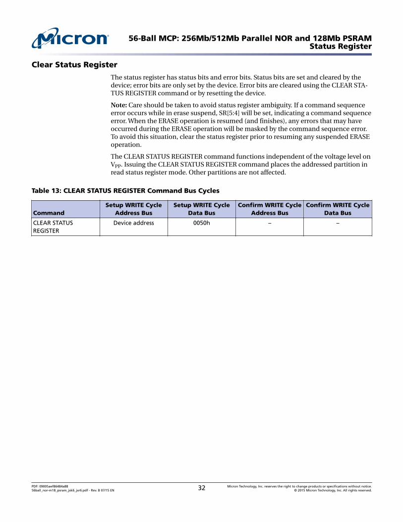
Clear Status Register
The status register has status bits and error bits. Status bits are set and cleared by thedevice; error bits are only set by the device. Error bits are cleared using the CLEAR STA-TUS REGISTER command or by resetting the device.
Note: Care should be taken to avoid status register ambiguity. If a command sequenceerror occurs while in erase suspend, SR[5:4] will be set, indicating a command sequenceerror. When the ERASE operation is resumed (and finishes), any errors that may haveoccurred during the ERASE operation will be masked by the command sequence error.To avoid this situation, clear the status register prior to resuming any suspended ERASEoperation.
The CLEAR STATUS REGISTER command functions independent of the voltage level onVPP. Issuing the CLEAR STATUS REGISTER command places the addressed partition inread status register mode. Other partitions are not affected.
Table 13: CLEAR STATUS REGISTER Command Bus Cycles
CommandSetup WRITE Cycle
Address BusSetup WRITE Cycle
Data BusConfirm WRITE Cycle
Address BusConfirm WRITE Cycle
Data Bus
CLEAR STATUSREGISTER
Device address 0050h – –
56-Ball MCP: 256Mb/512Mb Parallel NOR and 128Mb PSRAMStatus Register
PDF: 09005aef86484a8856ball_nor-m18_psram_jxk6_jxr6.pdf - Rev. B 07/15 EN 32 Micron Technology, Inc. reserves the right to change products or specifications without notice.
© 2015 Micron Technology, Inc. All rights reserved.
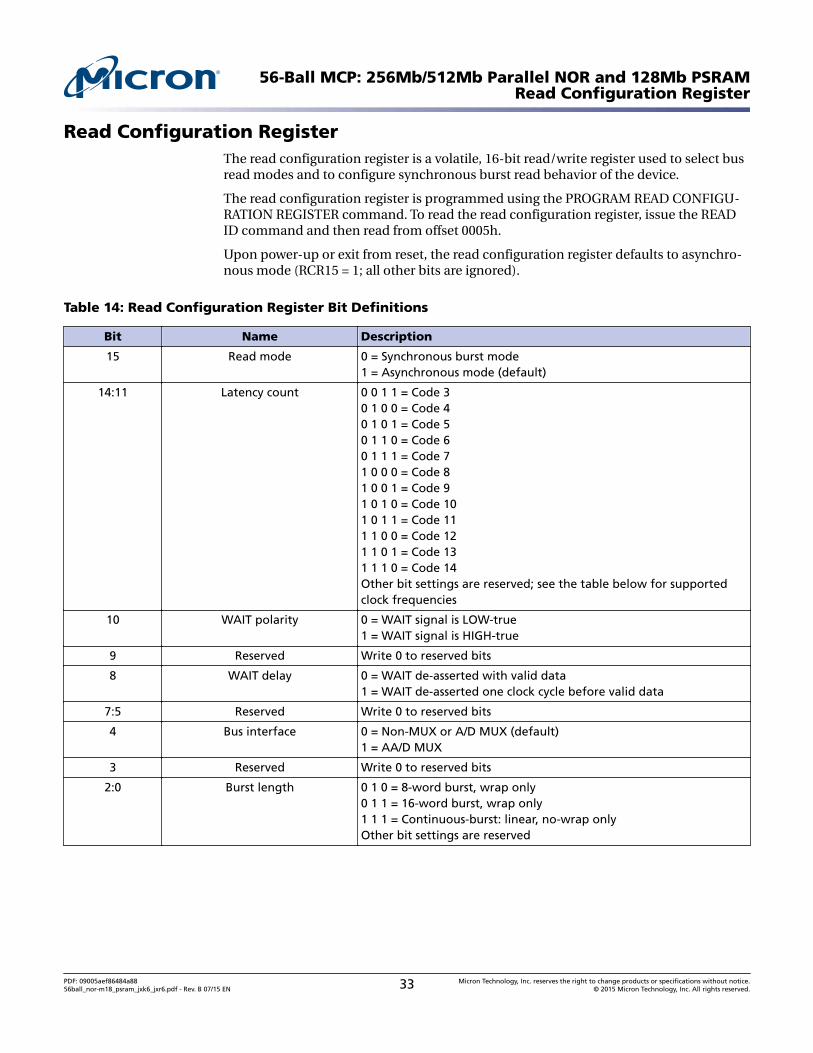
Read Configuration RegisterThe read configuration register is a volatile, 16-bit read/write register used to select busread modes and to configure synchronous burst read behavior of the device.
The read configuration register is programmed using the PROGRAM READ CONFIGU-RATION REGISTER command. To read the read configuration register, issue the READID command and then read from offset 0005h.
Upon power-up or exit from reset, the read configuration register defaults to asynchro-nous mode (RCR15 = 1; all other bits are ignored).
Table 14: Read Configuration Register Bit Definitions
Bit Name Description
15 Read mode 0 = Synchronous burst mode1 = Asynchronous mode (default)
14:11 Latency count 0 0 1 1 = Code 30 1 0 0 = Code 40 1 0 1 = Code 50 1 1 0 = Code 60 1 1 1 = Code 71 0 0 0 = Code 81 0 0 1 = Code 91 0 1 0 = Code 101 0 1 1 = Code 111 1 0 0 = Code 121 1 0 1 = Code 131 1 1 0 = Code 14Other bit settings are reserved; see the table below for supportedclock frequencies
10 WAIT polarity 0 = WAIT signal is LOW-true1 = WAIT signal is HIGH-true
9 Reserved Write 0 to reserved bits
8 WAIT delay 0 = WAIT de-asserted with valid data1 = WAIT de-asserted one clock cycle before valid data
7:5 Reserved Write 0 to reserved bits
4 Bus interface 0 = Non-MUX or A/D MUX (default)1 = AA/D MUX
3 Reserved Write 0 to reserved bits
2:0 Burst length 0 1 0 = 8-word burst, wrap only0 1 1 = 16-word burst, wrap only1 1 1 = Continuous-burst: linear, no-wrap onlyOther bit settings are reserved
56-Ball MCP: 256Mb/512Mb Parallel NOR and 128Mb PSRAMRead Configuration Register
PDF: 09005aef86484a8856ball_nor-m18_psram_jxk6_jxr6.pdf - Rev. B 07/15 EN 33 Micron Technology, Inc. reserves the right to change products or specifications without notice.
© 2015 Micron Technology, Inc. All rights reserved.
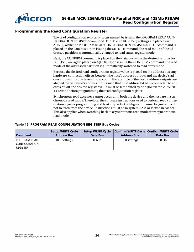
Programming the Read Configuration Register
The read configuration register is programmed by issuing the PROGRAM READ CON-FIGURATION REGISTER command. The desired RCR[15:0] settings are placed onA[15:0], while the PROGRAM READ CONFIGURATION REGISTER SETUP command isplaced on the data bus. Upon issuing the SETUP command, the read mode of the ad-dressed partition is automatically changed to read status register mode.
Next, the CONFIRM command is placed on the data bus while the desired settings forRCR[15:0] are again placed on A[15:0]. Upon issuing the CONFIRM command, the readmode of the addressed partition is automatically switched to read array mode.
Because the desired read configuration register value is placed on the address bus, anyhardware-connection offsets between the host’s address outputs and the device’s ad-dress inputs must be taken into account. For example, if the host’s address outputs arealigned to the device’s address inputs such that host address bit A1 is connected to ad-dress bit A0, the desired register value must be left-shifted by one (for example, 2532h<< 4A64h) before programming the read configuration register
Synchronous read accesses cannot occur until both the device and the host are in syn-chronous read mode. Therefore, the software instructions used to perform read config-uration register programming and host chip select configuration must be guaranteednot to fetch from the device (instructions must be in system RAM or locked in cache).This also applies when switching back to asynchronous read mode from synchronousread mode.
Table 15: PROGRAM READ CONFIGURATION REGISTER Bus Cycles
CommandSetup WRITE Cycle
Address BusSetup WRITE Cycle
Data BusConfirm WRITE Cycle
Address BusConfirm WRITE Cycle
Data Bus
PROGRAM READCONFIGURATIONREGISTER
RCR settings 0060h RCR settings 0003h
56-Ball MCP: 256Mb/512Mb Parallel NOR and 128Mb PSRAMRead Configuration Register
PDF: 09005aef86484a8856ball_nor-m18_psram_jxk6_jxr6.pdf - Rev. B 07/15 EN 34 Micron Technology, Inc. reserves the right to change products or specifications without notice.
© 2015 Micron Technology, Inc. All rights reserved.
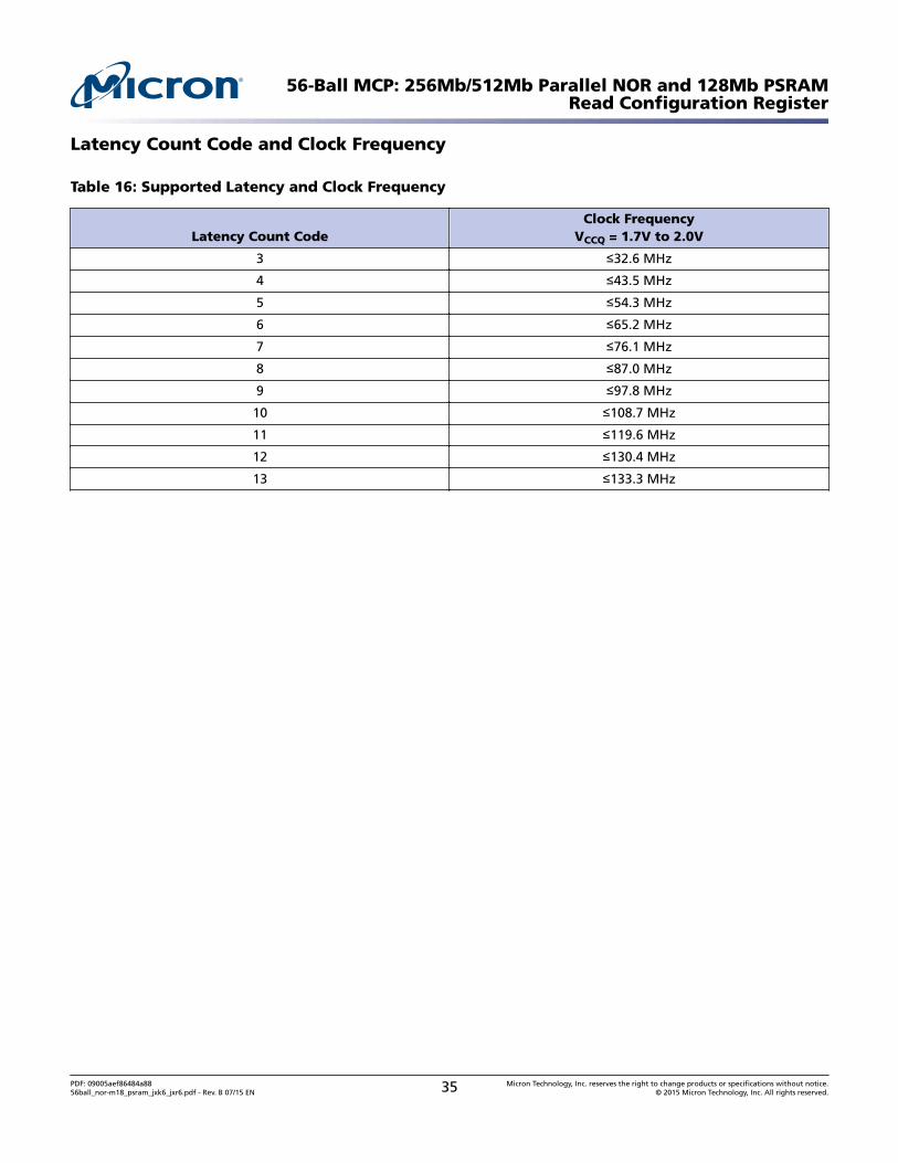
Latency Count Code and Clock Frequency
Table 16: Supported Latency and Clock Frequency
Latency Count CodeClock Frequency
VCCQ = 1.7V to 2.0V
3 ≤32.6 MHz
4 ≤43.5 MHz
5 ≤54.3 MHz
6 ≤65.2 MHz
7 ≤76.1 MHz
8 ≤87.0 MHz
9 ≤97.8 MHz
10 ≤108.7 MHz
11 ≤119.6 MHz
12 ≤130.4 MHz
13 ≤133.3 MHz
56-Ball MCP: 256Mb/512Mb Parallel NOR and 128Mb PSRAMRead Configuration Register
PDF: 09005aef86484a8856ball_nor-m18_psram_jxk6_jxr6.pdf - Rev. B 07/15 EN 35 Micron Technology, Inc. reserves the right to change products or specifications without notice.
© 2015 Micron Technology, Inc. All rights reserved.
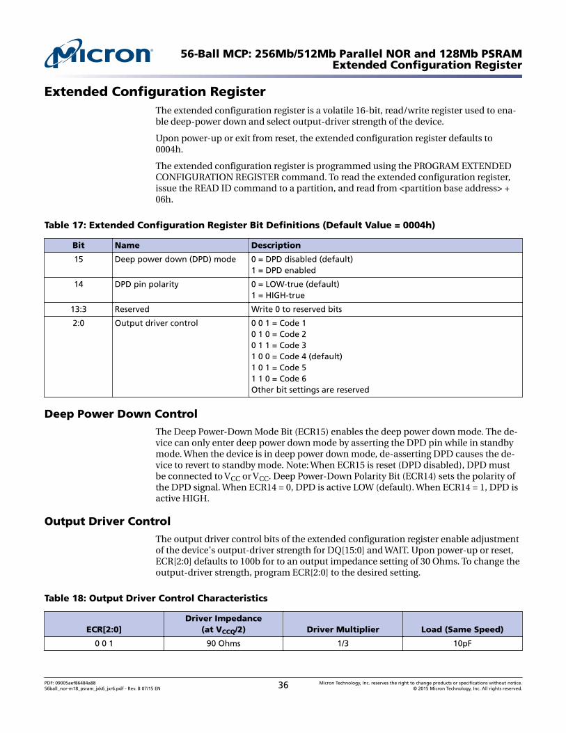
Extended Configuration RegisterThe extended configuration register is a volatile 16-bit, read/write register used to ena-ble deep-power down and select output-driver strength of the device.
Upon power-up or exit from reset, the extended configuration register defaults to0004h.
The extended configuration register is programmed using the PROGRAM EXTENDEDCONFIGURATION REGISTER command. To read the extended configuration register,issue the READ ID command to a partition, and read from <partition base address> +06h.
Table 17: Extended Configuration Register Bit Definitions (Default Value = 0004h)
Bit Name Description
15 Deep power down (DPD) mode 0 = DPD disabled (default)1 = DPD enabled
14 DPD pin polarity 0 = LOW-true (default)1 = HIGH-true
13:3 Reserved Write 0 to reserved bits
2:0 Output driver control 0 0 1 = Code 10 1 0 = Code 20 1 1 = Code 31 0 0 = Code 4 (default)1 0 1 = Code 51 1 0 = Code 6Other bit settings are reserved
Deep Power Down Control
The Deep Power-Down Mode Bit (ECR15) enables the deep power down mode. The de-vice can only enter deep power down mode by asserting the DPD pin while in standbymode. When the device is in deep power down mode, de-asserting DPD causes the de-vice to revert to standby mode. Note: When ECR15 is reset (DPD disabled), DPD mustbe connected to VCC or VCC. Deep Power-Down Polarity Bit (ECR14) sets the polarity ofthe DPD signal. When ECR14 = 0, DPD is active LOW (default). When ECR14 = 1, DPD isactive HIGH.
Output Driver Control
The output driver control bits of the extended configuration register enable adjustmentof the device’s output-driver strength for DQ[15:0] and WAIT. Upon power-up or reset,ECR[2:0] defaults to 100b for to an output impedance setting of 30 Ohms. To change theoutput-driver strength, program ECR[2:0] to the desired setting.
Table 18: Output Driver Control Characteristics
ECR[2:0]Driver Impedance
(at VCCQ/2) Driver Multiplier Load (Same Speed)
0 0 1 90 Ohms 1/3 10pF
56-Ball MCP: 256Mb/512Mb Parallel NOR and 128Mb PSRAMExtended Configuration Register
PDF: 09005aef86484a8856ball_nor-m18_psram_jxk6_jxr6.pdf - Rev. B 07/15 EN 36 Micron Technology, Inc. reserves the right to change products or specifications without notice.
© 2015 Micron Technology, Inc. All rights reserved.
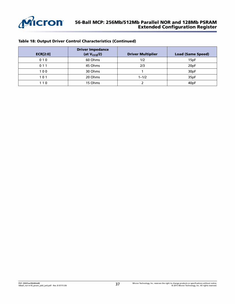
Table 18: Output Driver Control Characteristics (Continued)
ECR[2:0]Driver Impedance
(at VCCQ/2) Driver Multiplier Load (Same Speed)
0 1 0 60 Ohms 1/2 15pF
0 1 1 45 Ohms 2/3 20pF
1 0 0 30 Ohms 1 30pF
1 0 1 20 Ohms 1–1/2 35pF
1 1 0 15 Ohms 2 40pF
56-Ball MCP: 256Mb/512Mb Parallel NOR and 128Mb PSRAMExtended Configuration Register
PDF: 09005aef86484a8856ball_nor-m18_psram_jxk6_jxr6.pdf - Rev. B 07/15 EN 37 Micron Technology, Inc. reserves the right to change products or specifications without notice.
© 2015 Micron Technology, Inc. All rights reserved.
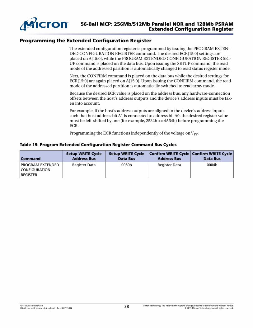
Programming the Extended Configuration Register
The extended configuration register is programmed by issuing the PROGRAM EXTEN-DED CONFIGURATION REGISTER command. The desired ECR[15:0] settings areplaced on A[15:0], while the PROGRAM EXTENDED CONFIGURATION REGISTER SET-UP command is placed on the data bus. Upon issuing the SETUP command, the readmode of the addressed partition is automatically changed to read status register mode.
Next, the CONFIRM command is placed on the data bus while the desired settings forECR[15:0] are again placed on A[15:0]. Upon issuing the CONFIRM command, the readmode of the addressed partition is automatically switched to read array mode.
Because the desired ECR value is placed on the address bus, any hardware-connectionoffsets between the host’s address outputs and the device’s address inputs must be tak-en into account.
For example, if the host’s address outputs are aligned to the device’s address inputssuch that host address bit A1 is connected to address bit A0, the desired register valuemust be left-shifted by one (for example, 2532h << 4A64h) before programming theECR.
Programming the ECR functions independently of the voltage on VPP.
Table 19: Program Extended Configuration Register Command Bus Cycles
CommandSetup WRITE Cycle
Address BusSetup WRITE Cycle
Data BusConfirm WRITE Cycle
Address BusConfirm WRITE Cycle
Data Bus
PROGRAM EXTENDEDCONFIGURATIONREGISTER
Register Data 0060h Register Data 0004h
56-Ball MCP: 256Mb/512Mb Parallel NOR and 128Mb PSRAMExtended Configuration Register
PDF: 09005aef86484a8856ball_nor-m18_psram_jxk6_jxr6.pdf - Rev. B 07/15 EN 38 Micron Technology, Inc. reserves the right to change products or specifications without notice.
© 2015 Micron Technology, Inc. All rights reserved.
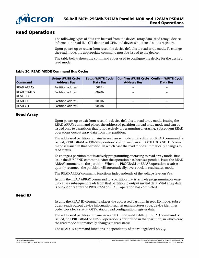
Read OperationsThe following types of data can be read from the device: array data (read array), deviceinformation (read ID), CFI data (read CFI), and device status (read status register).
Upon power-up or return from reset, the device defaults to read array mode. To changethe read mode, the appropriate command must be issued to the device.
The table below shows the command codes used to configure the device for the desiredread mode.
Table 20: READ MODE Command Bus Cycles
CommandSetup WRITE Cycle
Address BusSetup WRITE Cycle
Data BusConfirm WRITE Cycle
Address BusConfirm WRITE Cycle
Data Bus
READ ARRAY Partition address 00FFh – –
READ STATUSREGISTER
Partition address 0070h – –
READ ID Partition address 0090h – –
READ CFI Partition address 0098h – –
Read Array
Upon power-up or exit from reset, the device defaults to read array mode. Issuing theREAD ARRAY command places the addressed partition in read array mode and can beissued only to a partition that is not actively programming or erasing. Subsequent READoperations output array data from that partition.
The addressed partition remains in read array mode until a different READ command isissued, a PROGRAM or ERASE operation is performed, or a BLOCK LOCK SETUP com-mand is issued in that partition, in which case the read mode automatically changes toread status.
To change a partition that is actively programming or erasing to read array mode, firstissue the SUSPEND command. After the operation has been suspended, issue the READARRAY command to the partition. When the PROGRAM or ERASE operation is subse-quently resumed, the partition will automatically revert back to read status mode.
The READ ARRAY command functions independently of the voltage level on VPP.
Issuing the READ ARRAY command to a partition that is actively programming or eras-ing causes subsequent reads from that partition to output invalid data. Valid array datais output only after the PROGRAM or ERASE operation has completed.
Read ID
Issuing the READ ID command places the addressed partition in read ID mode. Subse-quent reads output device information such as manufacturer code, device identifiercode, block lock status, OTP data, or read configuration register data.
The addressed partition remains in read ID mode until a different READ command isissued, or a PROGRAM or ERASE operation is performed in that partition, in which casethe read mode automatically changes to read status.
The READ ID command functions independently of the voltage level on VPP.
56-Ball MCP: 256Mb/512Mb Parallel NOR and 128Mb PSRAMRead Operations
PDF: 09005aef86484a8856ball_nor-m18_psram_jxk6_jxr6.pdf - Rev. B 07/15 EN 39 Micron Technology, Inc. reserves the right to change products or specifications without notice.
© 2015 Micron Technology, Inc. All rights reserved.
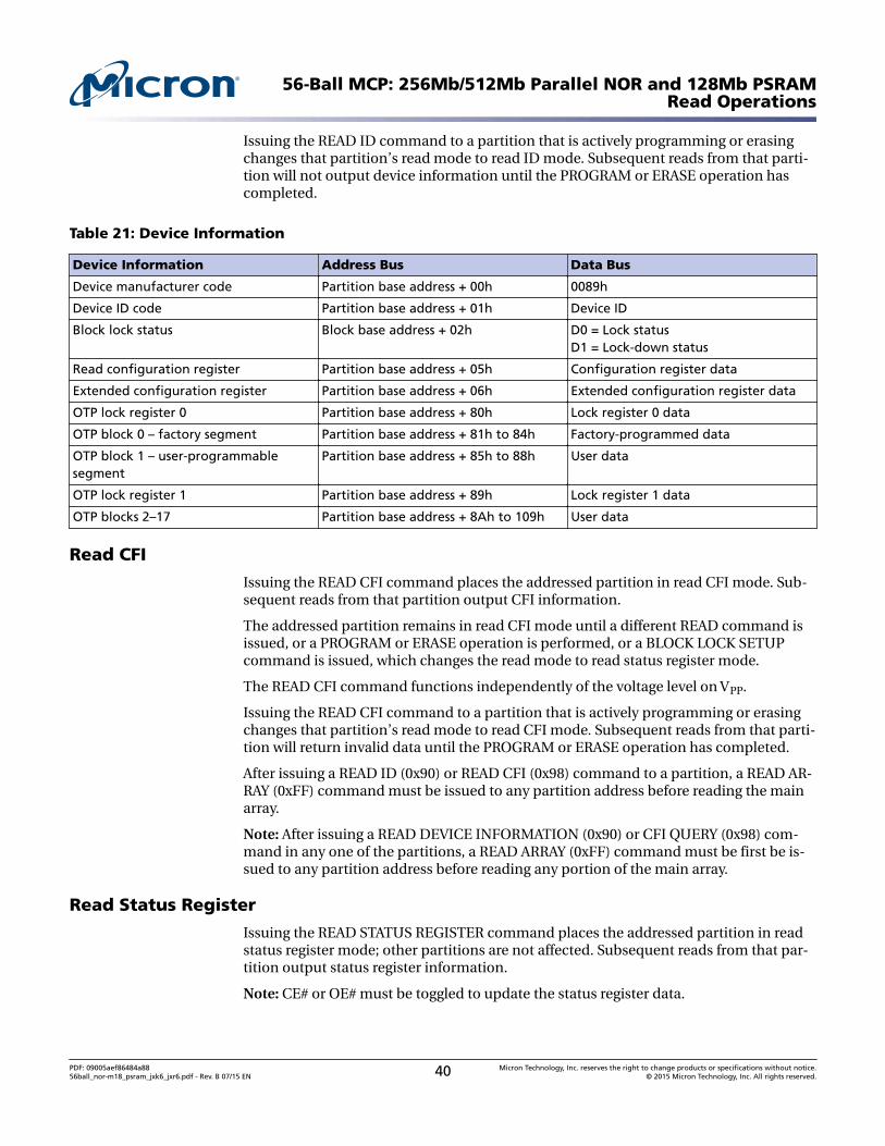
Issuing the READ ID command to a partition that is actively programming or erasingchanges that partition’s read mode to read ID mode. Subsequent reads from that parti-tion will not output device information until the PROGRAM or ERASE operation hascompleted.
Table 21: Device Information
Device Information Address Bus Data Bus
Device manufacturer code Partition base address + 00h 0089h
Device ID code Partition base address + 01h Device ID
Block lock status Block base address + 02h D0 = Lock statusD1 = Lock-down status
Read configuration register Partition base address + 05h Configuration register data
Extended configuration register Partition base address + 06h Extended configuration register data
OTP lock register 0 Partition base address + 80h Lock register 0 data
OTP block 0 – factory segment Partition base address + 81h to 84h Factory-programmed data
OTP block 1 – user-programmablesegment
Partition base address + 85h to 88h User data
OTP lock register 1 Partition base address + 89h Lock register 1 data
OTP blocks 2–17 Partition base address + 8Ah to 109h User data
Read CFI
Issuing the READ CFI command places the addressed partition in read CFI mode. Sub-sequent reads from that partition output CFI information.
The addressed partition remains in read CFI mode until a different READ command isissued, or a PROGRAM or ERASE operation is performed, or a BLOCK LOCK SETUPcommand is issued, which changes the read mode to read status register mode.
The READ CFI command functions independently of the voltage level on VPP.
Issuing the READ CFI command to a partition that is actively programming or erasingchanges that partition’s read mode to read CFI mode. Subsequent reads from that parti-tion will return invalid data until the PROGRAM or ERASE operation has completed.
After issuing a READ ID (0x90) or READ CFI (0x98) command to a partition, a READ AR-RAY (0xFF) command must be issued to any partition address before reading the mainarray.
Note: After issuing a READ DEVICE INFORMATION (0x90) or CFI QUERY (0x98) com-mand in any one of the partitions, a READ ARRAY (0xFF) command must be first be is-sued to any partition address before reading any portion of the main array.
Read Status Register
Issuing the READ STATUS REGISTER command places the addressed partition in readstatus register mode; other partitions are not affected. Subsequent reads from that par-tition output status register information.
Note: CE# or OE# must be toggled to update the status register data.
56-Ball MCP: 256Mb/512Mb Parallel NOR and 128Mb PSRAMRead Operations
PDF: 09005aef86484a8856ball_nor-m18_psram_jxk6_jxr6.pdf - Rev. B 07/15 EN 40 Micron Technology, Inc. reserves the right to change products or specifications without notice.
© 2015 Micron Technology, Inc. All rights reserved.
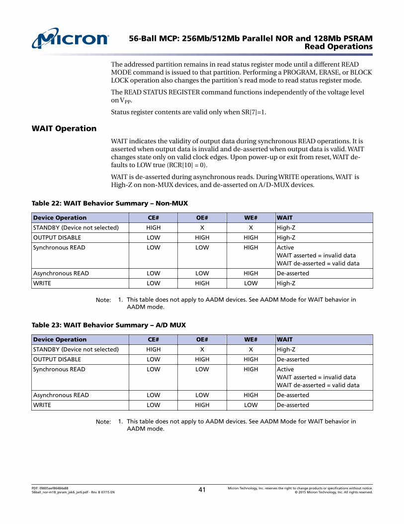
The addressed partition remains in read status register mode until a different READMODE command is issued to that partition. Performing a PROGRAM, ERASE, or BLOCKLOCK operation also changes the partition’s read mode to read status register mode.
The READ STATUS REGISTER command functions independently of the voltage levelon VPP.
Status register contents are valid only when SR[7]=1.
WAIT Operation
WAIT indicates the validity of output data during synchronous READ operations. It isasserted when output data is invalid and de-asserted when output data is valid. WAITchanges state only on valid clock edges. Upon power-up or exit from reset, WAIT de-faults to LOW true (RCR[10] = 0).
WAIT is de-asserted during asynchronous reads. During WRITE operations, WAIT isHigh-Z on non-MUX devices, and de-asserted on A/D-MUX devices.
Table 22: WAIT Behavior Summary – Non-MUX
Device Operation CE# OE# WE# WAIT
STANDBY (Device not selected) HIGH X X High-Z
OUTPUT DISABLE LOW HIGH HIGH High-Z
Synchronous READ LOW LOW HIGH ActiveWAIT asserted = invalid dataWAIT de-asserted = valid data
Asynchronous READ LOW LOW HIGH De-asserted
WRITE LOW HIGH LOW High-Z
Note: 1. This table does not apply to AADM devices. See AADM Mode for WAIT behavior inAADM mode.
Table 23: WAIT Behavior Summary – A/D MUX
Device Operation CE# OE# WE# WAIT
STANDBY (Device not selected) HIGH X X High-Z
OUTPUT DISABLE LOW HIGH HIGH De-asserted
Synchronous READ LOW LOW HIGH ActiveWAIT asserted = invalid dataWAIT de-asserted = valid data
Asynchronous READ LOW LOW HIGH De-asserted
WRITE LOW HIGH LOW De-asserted
Note: 1. This table does not apply to AADM devices. See AADM Mode for WAIT behavior inAADM mode.
56-Ball MCP: 256Mb/512Mb Parallel NOR and 128Mb PSRAMRead Operations
PDF: 09005aef86484a8856ball_nor-m18_psram_jxk6_jxr6.pdf - Rev. B 07/15 EN 41 Micron Technology, Inc. reserves the right to change products or specifications without notice.
© 2015 Micron Technology, Inc. All rights reserved.
Programming ModesEach programming region in a block can be configured for either control mode or ob-ject mode.
The programming mode is automatically set based on the data pattern when a region isfirst programmed. Selecting either control mode or object mode is done according tothe specific needs of the system. In control mode, code or data is frequently changed(such as the flash file system or header information). In object mode, large code or data(such as objects or payloads) is infrequently changed. By implementing the appropriateprogramming mode, software can efficiently organize how information is stored in thememory array.
Control mode programming regions and object mode programming regions can be in-termingled within the same erase block. However, the programming mode of any regionwithin a block can be changed only after erasing the entire block.
Control Mode
Control mode programming is invoked when only the A-half (A3 = 0) of the program-ming region is programmed to 0s. The B-half (A3 = 1) remains erased. Control mode al-lows up to 512 bytes of data to be programmed in the region. The information can beprogrammed in bits, bytes, or words.
Control mode supports the following programming methods:
• Single-word programming (0041h)• Buffered programming (00E9h/00D0h)• Buffered enhanced factory programming (0080h/00D0h)
When buffered programming is used in control mode, all addresses must be in the A-half of the buffer (A3 = 0). During buffer fill, the B-half (A3 = 1) addresses do not need tobe filled with 0xFFFF.
Control mode programming is useful for storing dynamic information, such as flash filesystem headers, file Info, and so on. Typically, control mode programming does not re-quire the entire 512 bytes of data to be programmed at once. It may also contain datathat is changed after initial programming using a technique known as “bit twiddling”.Header information can be augmented later with additional new information within acontrol-mode-programmed region. This allows implementation of legacy file systems,as well as transaction-based power-loss recovery.
In a control mode region, PROGRAM operations can be performed multiple times.However, care must be taken to avoid programming any zeros in the B-half (A3 = 1) ofthe region. Violation of this usage will cause SR[4] and SR[9] to be set, and the PRO-GRAM operation will be aborted.
56-Ball MCP: 256Mb/512Mb Parallel NOR and 128Mb PSRAMProgramming Modes
PDF: 09005aef86484a8856ball_nor-m18_psram_jxk6_jxr6.pdf - Rev. B 07/15 EN 42 Micron Technology, Inc. reserves the right to change products or specifications without notice.
© 2015 Micron Technology, Inc. All rights reserved.
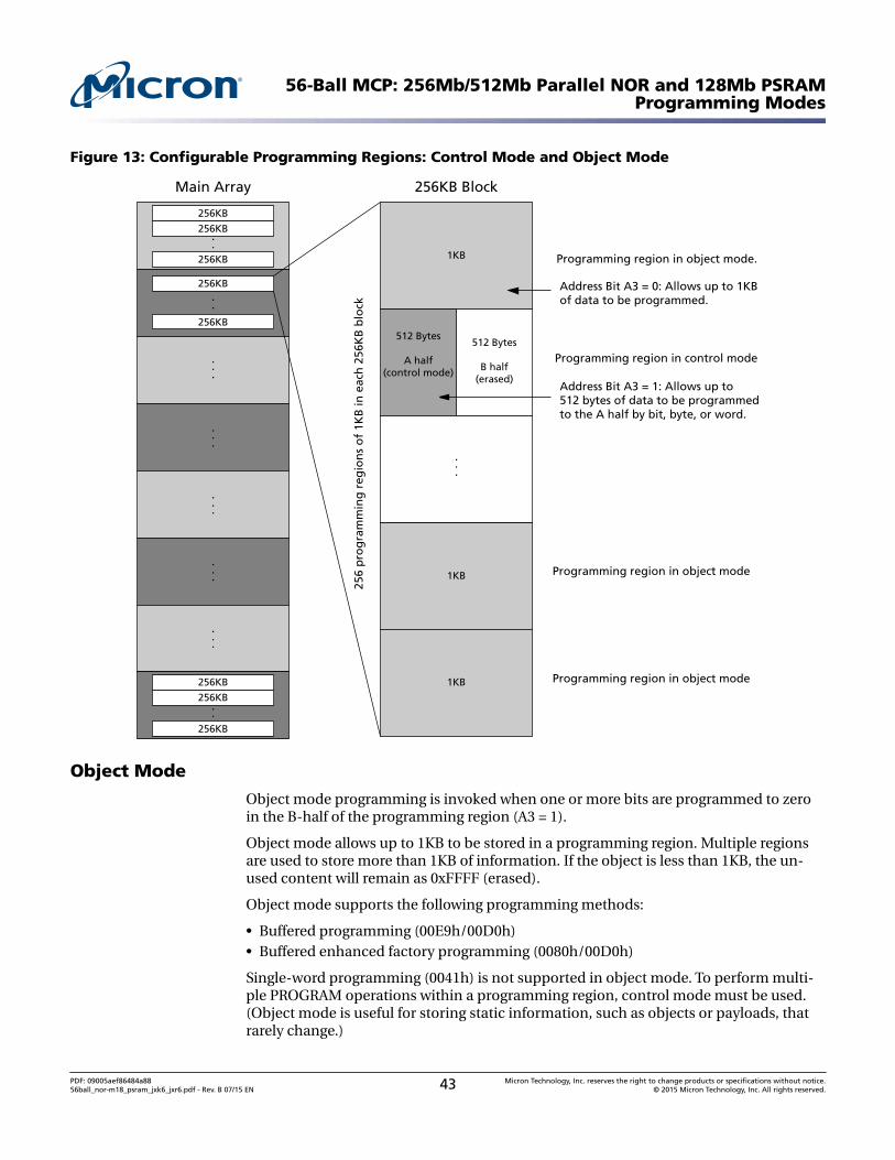
Figure 13: Configurable Programming Regions: Control Mode and Object Mode
Main Array
256
pro
gra
mm
ing
reg
ion
s o
f 1K
B in
eac
h 2
56K
B b
lock
256KB
256KB
256KB
.
.
256KB
256KB
.
.
.
.
.
.
.
.
.
.
.
.
.
.
.
.
.
256KB
256KB
256KB
.
.
256KB Block
Programming region in object mode.
Programming region in control mode
512 Bytes
A half(control mode)
1KB
Address Bit A3 = 1: Allows up to512 bytes of data to be programmedto the A half by bit, byte, or word.
512 Bytes
B half(erased)
Address Bit A3 = 0: Allows up to 1KBof data to be programmed.
Programming region in object mode
Programming region in object mode1KB
1KB
.
.
.
Object Mode
Object mode programming is invoked when one or more bits are programmed to zeroin the B-half of the programming region (A3 = 1).
Object mode allows up to 1KB to be stored in a programming region. Multiple regionsare used to store more than 1KB of information. If the object is less than 1KB, the un-used content will remain as 0xFFFF (erased).
Object mode supports the following programming methods:
• Buffered programming (00E9h/00D0h)• Buffered enhanced factory programming (0080h/00D0h)
Single-word programming (0041h) is not supported in object mode. To perform multi-ple PROGRAM operations within a programming region, control mode must be used.(Object mode is useful for storing static information, such as objects or payloads, thatrarely change.)
56-Ball MCP: 256Mb/512Mb Parallel NOR and 128Mb PSRAMProgramming Modes
PDF: 09005aef86484a8856ball_nor-m18_psram_jxk6_jxr6.pdf - Rev. B 07/15 EN 43 Micron Technology, Inc. reserves the right to change products or specifications without notice.
© 2015 Micron Technology, Inc. All rights reserved.
Once the programming region is configured in object mode, it cannot be augmented oroverwritten without first erasing the entire block containing the region. SubsequentPROGRAM operations to a programming region configured in object mode will causeSR[4] and SR[8] to be set and the PROGRAM operation to be aborted.
Issuing the 41h command to the B-half of an erased region will set error bits SR[8] andSR[9], and the PROGRAM operation will not proceed.
56-Ball MCP: 256Mb/512Mb Parallel NOR and 128Mb PSRAMProgramming Modes
PDF: 09005aef86484a8856ball_nor-m18_psram_jxk6_jxr6.pdf - Rev. B 07/15 EN 44 Micron Technology, Inc. reserves the right to change products or specifications without notice.
© 2015 Micron Technology, Inc. All rights reserved.
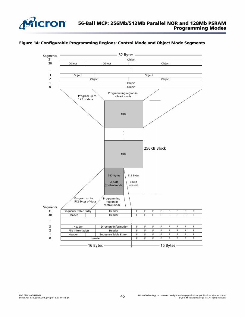
Figure 14: Configurable Programming Regions: Control Mode and Object Mode Segments
256KB Block
F F F F F F F FSequence Table Entry HeaderF F F F F F F FHeaderHeader
ObjectObject
Object
ObjectObject
Object
ObjectObject ObjectObject
32 Bytes
1KB
Program up to1KB of data
.
.
Programming region in object mode
512 Bytes
B half(erased)
512 Bytes
A half(control mode)
1KB
16 Bytes16 Bytes
Segments3130
...
3210
.
.
Program up to512 Bytes of data
Programming region in
control mode
HeaderHeader
File Information HeaderHeader Directory Information
Sequence Table EntryF F F F F F F FF F F F F F F FF F F F F F F F
F F F F F F F F
.
.
.
Segments3130
...
3210
56-Ball MCP: 256Mb/512Mb Parallel NOR and 128Mb PSRAMProgramming Modes
PDF: 09005aef86484a8856ball_nor-m18_psram_jxk6_jxr6.pdf - Rev. B 07/15 EN 45 Micron Technology, Inc. reserves the right to change products or specifications without notice.
© 2015 Micron Technology, Inc. All rights reserved.
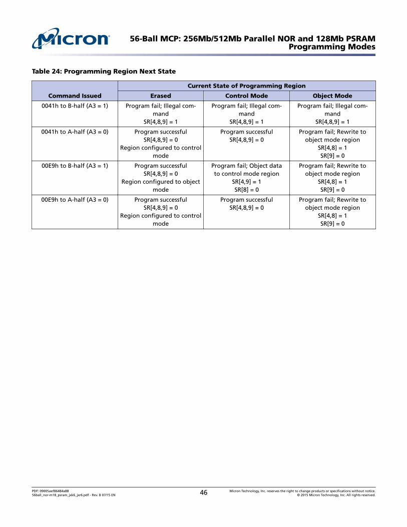
Table 24: Programming Region Next State
Command Issued
Current State of Programming Region
Erased Control Mode Object Mode
0041h to B-half (A3 = 1) Program fail; Illegal com-mand
SR[4,8,9] = 1
Program fail; Illegal com-mand
SR[4,8,9] = 1
Program fail; Illegal com-mand
SR[4,8,9] = 1
0041h to A-half (A3 = 0) Program successfulSR[4,8,9] = 0
Region configured to controlmode
Program successfulSR[4,8,9] = 0
Program fail; Rewrite toobject mode region
SR[4,8] = 1SR[9] = 0
00E9h to B-half (A3 = 1) Program successfulSR[4,8,9] = 0
Region configured to objectmode
Program fail; Object datato control mode region
SR[4,9] = 1SR[8] = 0
Program fail; Rewrite toobject mode region
SR[4,8] = 1SR[9] = 0
00E9h to A-half (A3 = 0) Program successfulSR[4,8,9] = 0
Region configured to controlmode
Program successfulSR[4,8,9] = 0
Program fail; Rewrite toobject mode region
SR[4,8] = 1SR[9] = 0
56-Ball MCP: 256Mb/512Mb Parallel NOR and 128Mb PSRAMProgramming Modes
PDF: 09005aef86484a8856ball_nor-m18_psram_jxk6_jxr6.pdf - Rev. B 07/15 EN 46 Micron Technology, Inc. reserves the right to change products or specifications without notice.
© 2015 Micron Technology, Inc. All rights reserved.
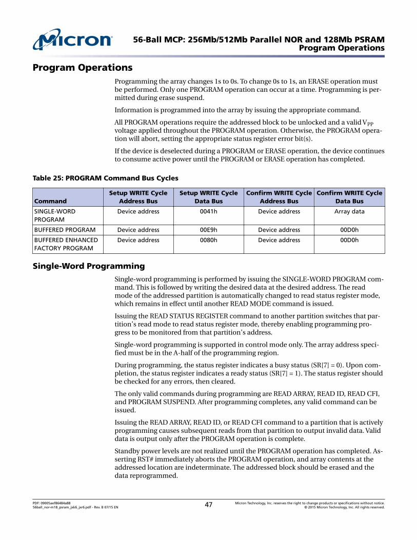
Program OperationsProgramming the array changes 1s to 0s. To change 0s to 1s, an ERASE operation mustbe performed. Only one PROGRAM operation can occur at a time. Programming is per-mitted during erase suspend.
Information is programmed into the array by issuing the appropriate command.
All PROGRAM operations require the addressed block to be unlocked and a valid VPPvoltage applied throughout the PROGRAM operation. Otherwise, the PROGRAM opera-tion will abort, setting the appropriate status register error bit(s).
If the device is deselected during a PROGRAM or ERASE operation, the device continuesto consume active power until the PROGRAM or ERASE operation has completed.
Table 25: PROGRAM Command Bus Cycles
CommandSetup WRITE Cycle
Address BusSetup WRITE Cycle
Data BusConfirm WRITE Cycle
Address BusConfirm WRITE Cycle
Data Bus
SINGLE-WORDPROGRAM
Device address 0041h Device address Array data
BUFFERED PROGRAM Device address 00E9h Device address 00D0h
BUFFERED ENHANCEDFACTORY PROGRAM
Device address 0080h Device address 00D0h
Single-Word Programming
Single-word programming is performed by issuing the SINGLE-WORD PROGRAM com-mand. This is followed by writing the desired data at the desired address. The readmode of the addressed partition is automatically changed to read status register mode,which remains in effect until another READ MODE command is issued.
Issuing the READ STATUS REGISTER command to another partition switches that par-tition’s read mode to read status register mode, thereby enabling programming pro-gress to be monitored from that partition’s address.
Single-word programming is supported in control mode only. The array address speci-fied must be in the A-half of the programming region.
During programming, the status register indicates a busy status (SR[7] = 0). Upon com-pletion, the status register indicates a ready status (SR[7] = 1). The status register shouldbe checked for any errors, then cleared.
The only valid commands during programming are READ ARRAY, READ ID, READ CFI,and PROGRAM SUSPEND. After programming completes, any valid command can beissued.
Issuing the READ ARRAY, READ ID, or READ CFI command to a partition that is activelyprogramming causes subsequent reads from that partition to output invalid data. Validdata is output only after the PROGRAM operation is complete.
Standby power levels are not realized until the PROGRAM operation has completed. As-serting RST# immediately aborts the PROGRAM operation, and array contents at theaddressed location are indeterminate. The addressed block should be erased and thedata reprogrammed.
56-Ball MCP: 256Mb/512Mb Parallel NOR and 128Mb PSRAMProgram Operations
PDF: 09005aef86484a8856ball_nor-m18_psram_jxk6_jxr6.pdf - Rev. B 07/15 EN 47 Micron Technology, Inc. reserves the right to change products or specifications without notice.
© 2015 Micron Technology, Inc. All rights reserved.
Single-Word Programming
Single-word programming is performed by issuing the SINGLE-WORD PROGRAM com-mand. This is followed by writing the desired data at the desired address. The readmode of the addressed partition is automatically changed to read status register mode,which remains in effect until another READ MODE command is issued.
Issuing the READ STATUS REGISTER command to another partition switches that par-tition’s read mode to read status register mode, thereby enabling programming pro-gress to be monitored from that partition’s address.
Single-word programming is supported in control mode only. The array address speci-fied must be in the A-half of the programming region.
During programming, the status register indicates a busy status (SR[7] = 0). Upon com-pletion, the status register indicates a ready status (SR[7] = 1). The status register shouldbe checked for any errors, then cleared.
The only valid command during programming is PROGRAM SUSPEND. After program-ming completes, any valid command can be issued.
Issuing the READ ARRAY, READ ID, or READ CFI command to a partition that is activelyprogramming causes subsequent reads from that partition to output invalid data. Validdata is output only after the PROGRAM operation is complete.
Standby power levels are not realized until the PROGRAM operation has completed. As-serting RST# immediately aborts the PROGRAM operation, and array contents at theaddressed location are indeterminate. The addressed block should be erased and thedata reprogrammed.
Buffered Programming
Buffered programming programs multiple words simultaneously into the memory ar-ray. Data is first written to a programming buffer and then programmed into the arrayin buffer-sized increments, significantly reducing the effective word programming time.
Optimal performance and power consumption is realized only by aligning the startingaddress to buffer-sized boundaries within the array. Crossing a buffer-sized boundarycan cause the buffered programming time to double.
The BUFFERED PROGRAM operation consists of the following fixed, predefined se-quence of bus WRITE cycles: 1) Issue the SETUP command; 2) Issue a word count; 3)Fill the buffer with user data; and 4) Issue the CONFIRM command. Once the SETUPcommand has been issued to an address, subsequent bus WRITE cycles must use ad-dresses within the same block throughout the operation; otherwise, the operation willabort. Bus READ cycles are allowed at any time and at any address.
Note: VPP must be at VPPL or VPPH throughout the BUFFERED PROGRAM operation.
Upon programming completion, the status register indicates ready (SR7 = 1), and anyvalid command may be issued. A full status register check should be performed tocheck for any programming errors. If any error bits are set, the status register should becleared using the CLEAR STATUS REGISTER command.
A subsequent BUFFERED PROGRAM operation can be initiated by issuing another SET-UP command and repeating the buffered programming sequence. Any errors in the sta-tus register caused by a previous operation should first be cleared to prevent masking oferrors that may occur during a subsequent BUFFERED PROGRAM operation.
56-Ball MCP: 256Mb/512Mb Parallel NOR and 128Mb PSRAMProgram Operations
PDF: 09005aef86484a8856ball_nor-m18_psram_jxk6_jxr6.pdf - Rev. B 07/15 EN 48 Micron Technology, Inc. reserves the right to change products or specifications without notice.
© 2015 Micron Technology, Inc. All rights reserved.
Valid commands issued to the busy partition during array programming are READ AR-RAY, READ ID, READ CFI, READ STATUS, and PROGRAM SUSPEND.
Issuing the READ ARRAY, READ ID, or READ CFI command to a partition that is activelyprogramming causes subsequent reads from that partition to output invalid data. Validdata is output only after the PROGRAM operation has completed.
Buffered Programming
Buffered programming programs multiple words simultaneously into the memory ar-ray. Data is first written to a programming buffer and then programmed into the arrayin buffer-sized increments, significantly reducing the effective word programming time.
Optimal performance and power consumption is realized only by aligning the startingaddress to buffer-sized boundaries within the array. Crossing a buffer-sized boundarycan cause the buffered programming time to double.
The BUFFERED PROGRAM operation consists of the following fixed, predefined se-quence of bus WRITE cycles: 1) Issue the SETUP command; 2) Issue a word count; 3)Fill the buffer with user data; and 4) Issue the CONFIRM command. Once the SETUPcommand has been issued to an address, subsequent bus WRITE cycles must use ad-dresses within the same block throughout the operation; otherwise, the operation willabort. Bus READ cycles are allowed at any time and at any address.
Note: VPP must be at VPPL or VPPH throughout the BUFFERED PROGRAM operation.
Upon programming completion, the status register indicates ready (SR7 = 1), and anyvalid command may be issued. A full status register check should be performed tocheck for any programming errors. If any error bits are set, the status register should becleared using the CLEAR STATUS REGISTER command.
A subsequent BUFFERED PROGRAM operation can be initiated by issuing another SET-UP command and repeating the buffered programming sequence. Any errors in the sta-tus register caused by a previous operation should first be cleared to prevent masking oferrors that may occur during a subsequent BUFFERED PROGRAM operation.
Valid commands issued to the busy partition during array programming are READ STA-TUS and PROGRAM SUSPEND.
Issuing the READ ARRAY, READ ID, or READ CFI command to a partition that is activelyprogramming causes subsequent reads from that partition to output invalid data. Validdata is output only after the PROGRAM operation has completed.
Buffered Enhanced Factory Programming
Buffered enhanced factory programming (BEFP) improves programming performancethrough the use of the write buffer, elevated programming voltage (VPPH), and en-hanced programming algorithm. User data is written into the write buffer, and then thebuffer contents are automatically written into the array in buffer-sized increments.
Internal verification during programming (inherent to MLC technology) and status reg-ister error checking are used to determine proper completion of the PROGRAM opera-tion. This eliminates delays incurred when switching between SINGLE-WORD PRO-GRAM and VERIFY operations.
BEFP consists of the following three distinct phases:
1. Setup phase: VPPH and block lock checks
56-Ball MCP: 256Mb/512Mb Parallel NOR and 128Mb PSRAMProgram Operations
PDF: 09005aef86484a8856ball_nor-m18_psram_jxk6_jxr6.pdf - Rev. B 07/15 EN 49 Micron Technology, Inc. reserves the right to change products or specifications without notice.
© 2015 Micron Technology, Inc. All rights reserved.
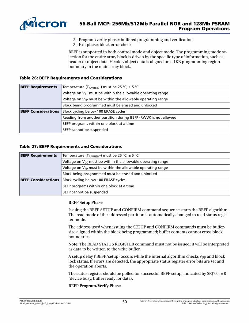
2. Program/verify phase: buffered programming and verification3. Exit phase: block error check
BEFP is supported in both control mode and object mode. The programming mode se-lection for the entire array block is driven by the specific type of information, such asheader or object data. Header/object data is aligned on a 1KB programming regionboundary in the main array block.
Table 26: BEFP Requirements and Considerations
BEFP Requirements Temperature (TAMBIENT) must be 25 °C, ± 5 °C
Voltage on VCC must be within the allowable operating range
Voltage on VPP must be within the allowable operating range
Block being programmed must be erased and unlocked
BEFP Considerations Block cycling below 100 ERASE cycles
Reading from another partition during BEFP (RWW) is not allowed
BEFP programs within one block at a time
BEFP cannot be suspended
Table 27: BEFP Requirements and Considerations
BEFP Requirements Temperature (TAMBIENT) must be 25 °C, ± 5 °C
Voltage on VCC must be within the allowable operating range
Voltage on VPP must be within the allowable operating range
Block being programmed must be erased and unlocked
BEFP Considerations Block cycling below 100 ERASE cycles
BEFP programs within one block at a time
BEFP cannot be suspended
BEFP Setup Phase
Issuing the BEFP SETUP and CONFIRM command sequence starts the BEFP algorithm.The read mode of the addressed partition is automatically changed to read status regis-ter mode.
The address used when issuing the SETUP and CONFIRM commands must be buffer-size aligned within the block being programmed; buffer contents cannot cross blockboundaries.
Note: The READ STATUS REGISTER command must not be issued; it will be interpretedas data to be written to the write buffer.
A setup delay (tBEFP/setup) occurs while the internal algorithm checks VPP and blocklock status. If errors are detected, the appropriate status register error bits are set andthe operation aborts.
The status register should be polled for successful BEFP setup, indicated by SR[7:0] = 0(device busy, buffer ready for data).
BEFP Program/Verify Phase
56-Ball MCP: 256Mb/512Mb Parallel NOR and 128Mb PSRAMProgram Operations
PDF: 09005aef86484a8856ball_nor-m18_psram_jxk6_jxr6.pdf - Rev. B 07/15 EN 50 Micron Technology, Inc. reserves the right to change products or specifications without notice.
© 2015 Micron Technology, Inc. All rights reserved.
Data is first written into the write buffer, then programmed into the array. During thebuffer fill sequence, the address used must be buffer-size aligned. Use of any other ad-dress will cause the operation to abort with a program fail error, and any data previouslyloaded in the buffer will not be programmed into the array.
The buffer fill data is stored in sequential buffer locations starting at address 00h. Aword count equal to the maximum buffer size is used; therefore, the buffer must becompletely filled. If the amount of data is less than the maximum buffer size, the re-maining buffer locations must be padded with FFFFh to completely fill the buffer.
Array programming starts as soon as the write buffer is full. Data words from the writebuffer are programmed into sequential array locations. SR0 = 1 indicates the write buf-fer is not available while the BEFP algorithm programs the array.
The status register should be polled for SR0 = 0 (buffer ready for data) to determinewhen the array programming has completed and the write buffer is again available forloading. The internal address is automatically incremented to enable subsequent arrayprogramming to continue from where the previous buffer-fill/array program sequenceended within the block. This cycle can be repeated to program the entire block.
BEFP Exit Phase
To exit the program/verify phase, write FFFFh to an address outside of the block.
The status register should be polled for SR7 = 1 (device ready), indicating the BEFP algo-rithm has finished running and the device has returned to normal operation.
A full status register error check should be performed to ensure the block was program-med successfully.
56-Ball MCP: 256Mb/512Mb Parallel NOR and 128Mb PSRAMProgram Operations
PDF: 09005aef86484a8856ball_nor-m18_psram_jxk6_jxr6.pdf - Rev. B 07/15 EN 51 Micron Technology, Inc. reserves the right to change products or specifications without notice.
© 2015 Micron Technology, Inc. All rights reserved.
Erase Operations
BLOCK ERASE
Erasing a block changes 0s to 1s. To change 1s to 0s, a PROGRAM operation must beperformed. Erasing is performed on a block basis; an entire block is erased each time anerase command sequence is issued. Once a block is fully erased, all addressable loca-tions within that block read as logical 1s (FFFFh).
Only one BLOCK ERASE operation can occur at a time. A BLOCK ERASE operation isnot permitted during program suspend. All BLOCK ERASE operations require the ad-dressed block to be unlocked, and VPP must be at VPPL or VPPH throughout the BLOCKERASE operation. Otherwise, the operation aborts, setting the appropriate status regis-ter error bit(s).
To perform a BLOCK ERASE operation, issue the BLOCK ERASE SETUP command at thedesired block address. The read mode of the addressed partition automatically changesto read status register mode and remains in effect until another READ MODE commandis issued.
The ERASE CONFIRM command latches the address of the block to be erased. The ad-dressed block is preconditioned (programmed to all 0s), erased, and then verified.
Issuing the READ STATUS REGISTER command to another partition switches that par-tition’s read mode to the read status register, thereby allowing block erase progress to bemonitored from that partition’s address. SR0 indicates whether the addressed partitionor the other partition is erasing.
During a BLOCK ERASE operation, the status register indicates a busy status (SR[7] = 0).
Issuing the READ ARRAY command to a partition that is actively erasing a main blockcauses subsequent reads from that partition to output invalid data. Valid array data isoutput only after the BLOCK ERASE operation has finished.
Upon completion, the status register indicates a ready status (SR[7] = 1). The status reg-ister should be checked for any errors, and then cleared.
If the device is deselected during an ERASE operation, the device continues to consumeactive power until the ERASE operation is completed.
Asserting RST# immediately aborts the BLOCK ERASE operation, and array contents atthe addressed location are indeterminate. The addressed block should be erased again.
The only valid commands during a BLOCK ERASE operation are READ ARRAY, READ ID,READ CFI, and ERASE SUSPEND. After the BLOCK ERASE operation has completed,any valid command can be issued.
The only valid command during a BLOCK ERASE operation is ERASE SUSPEND. Afterthe BLOCK ERASE operation has completed, any valid command can be issued.
Table 28: ERASE Command Bus Cycle
CommandSetup WRITE Cycle
Address BusSetup WRITE Cycle
Data BusConfirm WRITE Cycle
Address BusConfirm WRITE Cycle
Data Bus
BLOCK ERASE Device address 0020h Block address 00D0h
56-Ball MCP: 256Mb/512Mb Parallel NOR and 128Mb PSRAMErase Operations
PDF: 09005aef86484a8856ball_nor-m18_psram_jxk6_jxr6.pdf - Rev. B 07/15 EN 52 Micron Technology, Inc. reserves the right to change products or specifications without notice.
© 2015 Micron Technology, Inc. All rights reserved.
SUSPEND and RESUME OperationsPROGRAM and ERASE operations of the main array can be suspended to perform otherdevice operations, and then subsequently resumed. OTP area programming operationscannot be suspended. During erase suspend or program suspend, the addressed blockmust remain unlocked, VPP must be at VPPL or VPPH, and WP# must remain unchanged.Otherwise, the ERASE or PROGRAM operation will abort, setting the appropriate statusregister error bit(s).
SUSPEND Operation
To suspend an ongoing ERASE or PROGRAM operation, issue the SUSPEND commandto any device address. Issuing the SUSPEND command does not change the read mode.
Upon issuing a SUSPEND command, the ongoing ERASE or PROGRAM operation sus-pends after a delay of tSUSP. The operation is suspended only when SR[7:6] = 1 (erasesuspend) or SR[7:2] = 1 (program suspend).
While suspended, reading from a block that was being erased or programmed is not al-lowed. Also, programming within an erase suspended block is not allowed, and if at-tempted, will result in a programming error (SR[4] = 1). Erasing under program suspendis not allowed. However, array programming under erase suspend is allowed, and canalso be suspended. This results in a simultaneous erase suspend and program suspendcondition, indicated by SR[7:6,2] = 1. Additional valid commands while suspended areREAD ARRAY, READ STATUS REGISTER, READ ID, READ CFI, CLEAR STATUS REGIS-TER, and RESUME. No other commands are allowed.
During suspend, CE# may be de-asserted, placing the device in standby and reducingactive current to standby levels. VPP must remain at VPPL or VPPH, and WP# must remainunchanged.
Asserting RST# aborts any suspended BLOCK ERASE and PROGRAM operations; arraycontents at the addressed locations will be indeterminate.
During suspend, CE# may be de-asserted. The device is placed in standby, reducing ac-tive current. VPP must remain at VPPL or VPPH, and WP# must remain unchanged.
Asserting RST# aborts suspended BLOCK ERASE and PROGRAM operations; array con-tents at the addressed locations are indeterminate.
A BUFFERED PROGRAM command sequence can be terminated during a the BUFFERFILL operation while in an erase suspend by issuing any non-00D0h command (non-confirm command) to the same block address to which the BUFFERED PROGRAMcommand was written.
Table 29: Valid Commands During Suspend
Device Command Program Suspend Erase Suspend
READ ARRAY Allowed Allowed
READ STATUS REGISTER Allowed Allowed
CLEAR STATUS REGISTER Allowed Allowed
READ DEVICE INFORMATION Allowed Allowed
CFI QUERY Allowed Allowed
WORD PROGRAM Not Allowed Allowed
56-Ball MCP: 256Mb/512Mb Parallel NOR and 128Mb PSRAMSUSPEND and RESUME Operations
PDF: 09005aef86484a8856ball_nor-m18_psram_jxk6_jxr6.pdf - Rev. B 07/15 EN 53 Micron Technology, Inc. reserves the right to change products or specifications without notice.
© 2015 Micron Technology, Inc. All rights reserved.
Table 29: Valid Commands During Suspend (Continued)
Device Command Program Suspend Erase Suspend
BUFFERED PROGRAM Not Allowed Allowed
BUFFERED ENHANCED FACTORY PRO-GRAM
Not Allowed Not Allowed
BLOCK ERASE Not Allowed Not Allowed
PROGRAM/ERASE SUSPEND Not Allowed Not Allowed
PROGRAM/ERASE RESUME Allowed Allowed
RESUME Operation
To resume a suspended ERASE or PROGRAM operation, issue the RESUME commandto any device address. The ERASE or PROGRAM operation continues where it left off,and the respective status register suspend bit is cleared. Issuing the RESUME commanddoes not change the read mode.
When the RESUME command is issued during a simultaneous erase suspend or pro-gram suspend condition, the PROGRAM operation is resumed first. Upon completion ofthe PROGRAM operation, the status register should be checked for any errors, andcleared if needed. The RESUME command must be issued again to complete the ERASEoperation. Upon completion of the ERASE operation, the status register should bechecked for any errors, and cleared if needed.
Table 30: SUSPEND and RESUME Command Bus Cycles
CommandSetup WRITE Cycle
Address BusSetup WRITE Cycle
Data BusConfirm WRITE Cycle
Address BusConfirm WRITE Cycle
Data Bus
SUSPEND Device address 00B0h – –
RESUME Device address 00D0h – –
56-Ball MCP: 256Mb/512Mb Parallel NOR and 128Mb PSRAMSUSPEND and RESUME Operations
PDF: 09005aef86484a8856ball_nor-m18_psram_jxk6_jxr6.pdf - Rev. B 07/15 EN 54 Micron Technology, Inc. reserves the right to change products or specifications without notice.
© 2015 Micron Technology, Inc. All rights reserved.
BLANK CHECK OperationBlank check verifies whether a main-array block is completely erased. A BLANK CHECKoperation is performed one block at a time, and cannot be used during program sus-pend or erase suspend.
To use blank check, first issue the BLANK CHECK SETUP command followed by theCONFIRM command. The read mode of the addressed partition is automaticallychanged to read status register mode, which remains in effect until another read modeis issued.
During a BLANK CHECK operation, the status register indicates a busy status (SR[7] =0). Upon completion, the status register indicates a ready status (SR[7] = 1). Issuing theREAD STATUS REGISTER command to another partition switches that partition’s readmode to read status register mode, thereby allowing the BLANK CHECK operation to bemonitored from that partition’s address.
The status register should be checked for any errors, and then cleared. If theBLANKCHECK operation fails (the block is not completely erased), then the status register willindicate a blank check error (SR[7:5] = 1).
The only valid command during a BLANK CHECK operation is read status. Blank checkcannot be suspended. After the BLANK CHECK operation has completed, any validcommand can be issued.
Table 31: BLANK CHECK Command Bus Cycles
CommandSetup WRITE Cycle
Address BusSetup WRITE Cycle
Data BusConfirm WRITE Cycle
Address BusConfirm WRITE Cycle
Data Bus
BLANKCHECK
Block address 00BCh Block address 00D0h
56-Ball MCP: 256Mb/512Mb Parallel NOR and 128Mb PSRAMBLANK CHECK Operation
PDF: 09005aef86484a8856ball_nor-m18_psram_jxk6_jxr6.pdf - Rev. B 07/15 EN 55 Micron Technology, Inc. reserves the right to change products or specifications without notice.
© 2015 Micron Technology, Inc. All rights reserved.
Block LockTwo methods of block lock control are available: software and hardware. Software con-trol uses the BLOCK LOCK and BLOCK UNLOCK commands. Hardware control uses theBLOCK LOCK-DOWN command along with asserting WP#.
Upon power-up or exit from reset, all main array blocks are locked, but not lockeddown. Locked blocks cannot be erased or programmed. BLOCK LOCK and UNLOCKoperations are independent of the voltage level on VPP.
To lock, unlock, or lock-down a block, first issue the SETUP command to any addresswithin the desired block. The read mode of the addressed partition is automaticallychanged to read status register mode. Next, issue the desired CONFIRM command tothe block’s address. Note that the CONFIRM command determines the operation per-formed. The status register should be checked for any errors, and then cleared.
The lock status of a block can be determined by issuing the READ ID command, andthen reading from the block’s base address + 02h. See the table below table for the lock-bit settings.
Blocks cannot be locked or unlocked while being actively programmed or erased.Blocks can be locked or unlocked during erase suspend, but not during program sus-pend. If a BLOCK ERASE operation is suspended, and then the block is locked or lockeddown, the lock status of the block will be changed immediately. When resumed, theERASE operation will still complete.
Block lock-down protection is dependent on WP#. A locked-down block can only be un-locked by issuing the BLOCK UNLOCK command with WP# de-asserted. To return anunlocked block to the locked-down state, a BLOCK LOCK-DOWN command must be is-sued prior to asserting WP#.
When WP# = V IL, blocks locked down are locked, and cannot be unlocked using theBLOCK UNLOCK command.
When WP# = V IH, block lock-down protection is disabled; locked-down blocks can beindividually unlocked using the BLOCK UNLOCK command.
Subsequently, when WP# = V IL, previously locked-down blocks are once again lockedand locked-down, including locked-down blocks that may have been unlocked whileWP# was de-asserted.
Issuing the BLOCK LOCK-DOWN command to an unlocked block does not lock theblock. However, asserting WP# after issuing the BLOCK LOCK-DOWN command locks(and locks down) the block. Lock-down for all blocks is only cleared upon power-up orexit from reset.
Table 32: BLOCK LOCK Command Bus Cycles
CommandSetup WRITE Cycle
Address BusSetup WRITE Cycle
Data BusConfirm WRITE Cycle
Address BusConfirm WRITE Cycle
Data Bus
BLOCKLOCK
Block address 0060h Block address 0001h
BLOCK UN-LOCK
Block address 0060h Block address 00D0h
56-Ball MCP: 256Mb/512Mb Parallel NOR and 128Mb PSRAMBlock Lock
PDF: 09005aef86484a8856ball_nor-m18_psram_jxk6_jxr6.pdf - Rev. B 07/15 EN 56 Micron Technology, Inc. reserves the right to change products or specifications without notice.
© 2015 Micron Technology, Inc. All rights reserved.
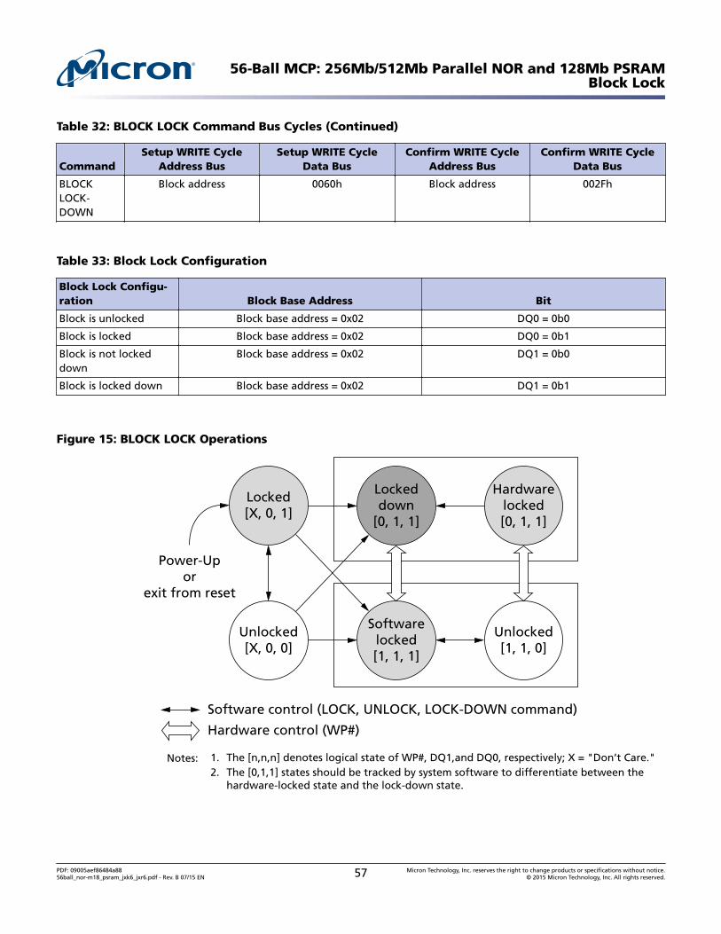
Table 32: BLOCK LOCK Command Bus Cycles (Continued)
CommandSetup WRITE Cycle
Address BusSetup WRITE Cycle
Data BusConfirm WRITE Cycle
Address BusConfirm WRITE Cycle
Data Bus
BLOCKLOCK-DOWN
Block address 0060h Block address 002Fh
Table 33: Block Lock Configuration
Block Lock Configu-ration Block Base Address Bit
Block is unlocked Block base address = 0x02 DQ0 = 0b0
Block is locked Block base address = 0x02 DQ0 = 0b1
Block is not lockeddown
Block base address = 0x02 DQ1 = 0b0
Block is locked down Block base address = 0x02 DQ1 = 0b1
Figure 15: BLOCK LOCK Operations
Locked[X, 0, 1]
Unlocked[X, 0, 0]
Lockeddown
[0, 1, 1]
Softwarelocked[1, 1, 1]
Hardwarelocked[0, 1, 1]
Unlocked[1, 1, 0]
Power-Upor
exit from reset
Software control (LOCK, UNLOCK, LOCK-DOWN command)
Hardware control (WP#)
Notes: 1. The [n,n,n] denotes logical state of WP#, DQ1,and DQ0, respectively; X = "Don’t Care."2. The [0,1,1] states should be tracked by system software to differentiate between the
hardware-locked state and the lock-down state.
56-Ball MCP: 256Mb/512Mb Parallel NOR and 128Mb PSRAMBlock Lock
PDF: 09005aef86484a8856ball_nor-m18_psram_jxk6_jxr6.pdf - Rev. B 07/15 EN 57 Micron Technology, Inc. reserves the right to change products or specifications without notice.
© 2015 Micron Technology, Inc. All rights reserved.

One-Time Programmable OperationsThe device contains sixteen 128-bit one-time programmable (OTP) blocks, two 64-bitOTP blocks, and two 16-bit OTP lock registers. OTP lock register 0 is used for lockingOTP blocks 0 and 1 (two 64-bit blocks), and OTP lock register 1 is used for locking OTPblocks 2 through 17 (sixteen 128-bit blocks).
Each block contains OTP bits that are factory set to 1 and can only be programmed from1 to 0; OTP block bits cannot be erased from 0 back to 1. This feature makes the OTPblocks particularly useful for implementing system-level security schemes, permanent-ly storing data, or storing fixed system parameters.
OTP block 0 is pre-programmed with a unique 64-bit value and locked at the factory.OTP block 1 contains all 1s and is user-programmable. OTP blocks 1 through 16 containall 1s and are user-programmable.
Each OTP block can be accessed multiple times to program individual bits, as long asthe block remains unlocked. When a lock register bit is programmed, the associatedOTP block can only be read—it can no longer be programmed.
OTP lock register bits lock out subsequent programming of the corresponding OTPblock. Each OTP block can be locked by programming its corresponding lock bit to 0. Aslong as an OTP block remains unlocked (that is, its lock bit = 1), any of its remaining 1bits can be programmed to 0.
Note: Once an OTP block is locked, it cannot be unlocked. Attempts to program alocked OTP block will fail with error bits set. Additionally, because the lock register bitsthemselves are OTP, when programmed, lock register bits cannot be erased. Therefore,when an OTP block is locked, it cannot be unlocked.
Table 34: Program OTP Area Command Bus Cycles
CommandSetup WRITE Cycle
Address BusSetup WRITE Cycle
Data BusConfirm WRITE Cycle
Address BusConfirm WRITE Cycle
Data Bus
PROGRAM OTP AREA Device address 00C0h OTP register address Register data
56-Ball MCP: 256Mb/512Mb Parallel NOR and 128Mb PSRAMOne-Time Programmable Operations
PDF: 09005aef86484a8856ball_nor-m18_psram_jxk6_jxr6.pdf - Rev. B 07/15 EN 58 Micron Technology, Inc. reserves the right to change products or specifications without notice.
© 2015 Micron Technology, Inc. All rights reserved.
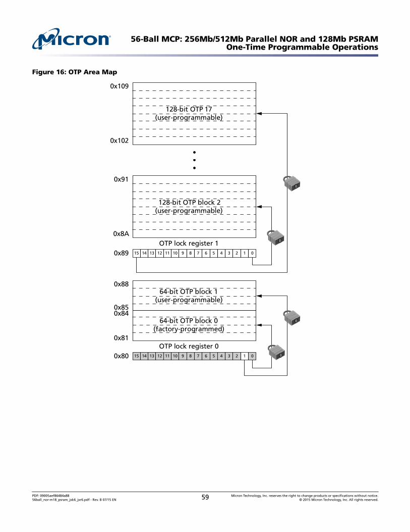
Figure 16: OTP Area Map
0x89OTP lock register 1
15 14 13 12 11 10 9 8 7 6 5 4 3 2 1 0
0x102
0x109
0x8A
0x91
128-bit OTP 17(user-programmable)
128-bit OTP block 2(user-programmable)
0x88
0x85
64-bit OTP block 1(user-programmable)
0x84
0x81
0x80OTP lock register 0
64-bit OTP block 0(factory-programmed)
15 14 13 12 11 10 9 8 7 6 5 4 3 2 1 0
56-Ball MCP: 256Mb/512Mb Parallel NOR and 128Mb PSRAMOne-Time Programmable Operations
PDF: 09005aef86484a8856ball_nor-m18_psram_jxk6_jxr6.pdf - Rev. B 07/15 EN 59 Micron Technology, Inc. reserves the right to change products or specifications without notice.
© 2015 Micron Technology, Inc. All rights reserved.
Programming OTP Area
OTP area programming is performed 16 bits at a time; only zeros within the data wordaffect any change to the OTP bits.
To program any OTP blocks or lock registers, first issue the PROGRAM OTP AREA SET-UP command at any device address. The read state of that partition changes to read sta-tus. Next, write the desired OTP data at the desired OTP address.
Attempting to program outside of the OTP area causes a program error (SR[4] = 1).
Attempting to program a locked OTP block causes a program error and a lock error(SR[4] = 1, SR[1] = 1).
OTP area programming cannot be suspended. Dual operations between the parameterpartition and the OTP area are not allowed.
Reading OTP Area
The OTP area is read from within the address space of any partition. To read from theOTP area. the following must be done:
1. Issue the READ ID command at the address of any partition to place that partitionin the read ID state.
2. Perform a READ operation at the base address of that partition, plus the addressoffset corresponding to the OTP word to be read. Data is read 16 bits at a time.
If a PROGRAM or ERASE operation occurs within the device while it is reading from theOTP area, certain restrictions may apply.
56-Ball MCP: 256Mb/512Mb Parallel NOR and 128Mb PSRAMOne-Time Programmable Operations
PDF: 09005aef86484a8856ball_nor-m18_psram_jxk6_jxr6.pdf - Rev. B 07/15 EN 60 Micron Technology, Inc. reserves the right to change products or specifications without notice.
© 2015 Micron Technology, Inc. All rights reserved.
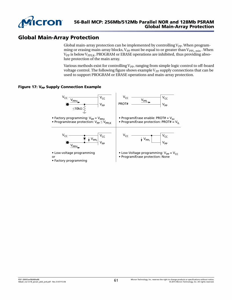
Global Main-Array ProtectionGlobal main-array protection can be implemented by controlling VPP. When program-ming or erasing main-array blocks, VPP must be equal to or greater than VPPL, min . WhenVPP is below VPPLK, PROGRAM or ERASE operations are inhibited, thus providing abso-lute protection of the main array.
Various methods exist for controlling VPP, ranging from simple logic control to off-boardvoltage control. The following figure shows example VPP supply connections that can beused to support PROGRAM or ERASE operations and main-array protection.
Figure 17: VPP Supply Connection Example
VCC VCCVPPH
VPPL
VPP
• Factory programming: VPP = VPPH• Program/erase protection: VPP ≤ VPPLK
VCC VCC
PROT# VPP
• Program/Erase enable: PROT# = VIH• Program/Erase protection: PROT# = VIL
VCC VCC
VPP
• Low-voltage programming or• Factory programming
VCC VCC
VPP
• Low-Voltage programming: VPP = VCC• Program/Erase protection: None
≤10kΩ
VPPL
VPPL
VPPH
56-Ball MCP: 256Mb/512Mb Parallel NOR and 128Mb PSRAMGlobal Main-Array Protection
PDF: 09005aef86484a8856ball_nor-m18_psram_jxk6_jxr6.pdf - Rev. B 07/15 EN 61 Micron Technology, Inc. reserves the right to change products or specifications without notice.
© 2015 Micron Technology, Inc. All rights reserved.
Dual OperationMultipartition architecture of the device enables reading from one partition while aPROGRAM or ERASE operation is occurring in another partition. This is called read-while-program and read-while-erase, respectively.
Only status reads are allowed from a partition that is busy programming or erasing. Ifnon-status reads are required from a partition that is busy programming or erasing, thePROGRAM or ERASE operation must be suspended first.
Table 35: Dual Operation Restrictions
The following table shows the allowed dual operations between array operations and non-array operations
ReadProgram or Erase
Main PartitionProgram OTP Area
Main Partition Yes (except busy partition) Yes (except busy partition)
Status Yes Yes
ID, OTP, or CFI Yes (except busy partition) No
56-Ball MCP: 256Mb/512Mb Parallel NOR and 128Mb PSRAMDual Operation
PDF: 09005aef86484a8856ball_nor-m18_psram_jxk6_jxr6.pdf - Rev. B 07/15 EN 62 Micron Technology, Inc. reserves the right to change products or specifications without notice.
© 2015 Micron Technology, Inc. All rights reserved.
Power and Reset Specifications
Initialization
Proper device initialization and operation is dependent on the power-up/down se-quence, reset procedure, and adequate power-supply decoupling.
Power-Up and Down
To avoid conditions that may result in spurious PROGRAM or ERASE operations, thepower sequences shown below are recommended. Note that each power supply mustbe at its minimum voltage range before applying or removing the next supply voltage inthe sequence. Also, device inputs must not be driven until all supply voltages have at-tained their minimum range, and RST# should be LOW during all power transitions.
When powering down the device, voltages should reach 0V before power is reapplied toensure proper device initialization. Otherwise, indeterminate operation could result.
When VCCQ goes below VLKOQ, the device is reset.
Table 36: Power Sequencing
Power Supply Power-Up Sequence Power-Down Sequence
VCC,min First First First1 First1 Third Second Second1 Second1
VCCQ,min Second Second1 First1 Second Second First1 Second1 First
VPP,min Third Second1 Second First1 First First1 First Second1
Note: 1. Connected/sequenced together.
Reset
During power-up and power-down, RST# should be asserted to prevent spurious PRO-GRAM or ERASE operations. While RST# is LOW, device operations are disabled, all in-puts such as address and control are ignored, and all outputs such as data and WAIT areplaced in High-Z. Invalid bus conditions are effectively masked out.
Upon power-up, RST# can be de-asserted after tVCCPH, allowing the device to exit fromreset. Upon exiting from reset, the device defaults to asynchronous read array mode,and the status register defaults to 0080h. Array data is available after tPHQV, or a busWRITE cycle can begin after tPHWL. If RST# is asserted during a PROGRAM or ERASEoperation, the operation will abort and array contents at that location will be invalid.
For proper system initialization, connect RST# to the LOW true reset signal that assertswhenever the processor is reset. This will ensure the device is in the expected readmode (read array) upon startup.
56-Ball MCP: 256Mb/512Mb Parallel NOR and 128Mb PSRAMPower and Reset Specifications
PDF: 09005aef86484a8856ball_nor-m18_psram_jxk6_jxr6.pdf - Rev. B 07/15 EN 63 Micron Technology, Inc. reserves the right to change products or specifications without notice.
© 2015 Micron Technology, Inc. All rights reserved.
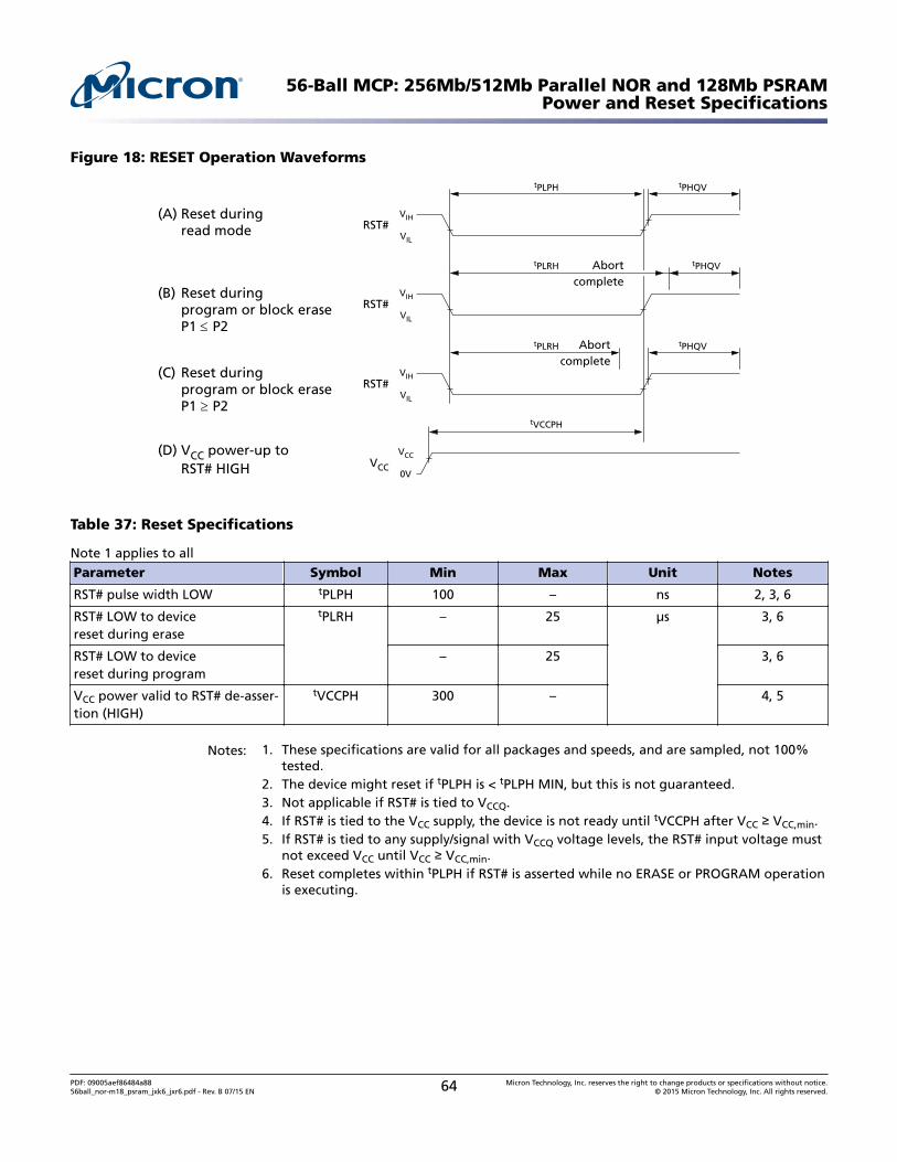
Figure 18: RESET Operation Waveforms
(A) Reset during read mode
VIH
VIL
RST#
(D) VCC power-up to RST# HIGH
tPLPH tPHQV
tPHQV
tPHQV
VCC
0VVCC
tVCCPH
(B) Reset during program or block erase P1 £ P2
VIH
VIL
RST#
Abortcomplete
Abortcomplete
tPLRH
(C) Reset during program or block erase P1 ³ P2
VIH
VIL
RST#
tPLRH
Table 37: Reset Specifications
Note 1 applies to allParameter Symbol Min Max Unit Notes
RST# pulse width LOW tPLPH 100 – ns 2, 3, 6
RST# LOW to devicereset during erase
tPLRH – 25 µs 3, 6
RST# LOW to devicereset during program
– 25 3, 6
VCC power valid to RST# de-asser-tion (HIGH)
tVCCPH 300 – 4, 5
Notes: 1. These specifications are valid for all packages and speeds, and are sampled, not 100%tested.
2. The device might reset if tPLPH is < tPLPH MIN, but this is not guaranteed.3. Not applicable if RST# is tied to VCCQ.4. If RST# is tied to the VCC supply, the device is not ready until tVCCPH after VCC ≥ VCC,min.5. If RST# is tied to any supply/signal with VCCQ voltage levels, the RST# input voltage must
not exceed VCC until VCC ≥ VCC,min.6. Reset completes within tPLPH if RST# is asserted while no ERASE or PROGRAM operation
is executing.
56-Ball MCP: 256Mb/512Mb Parallel NOR and 128Mb PSRAMPower and Reset Specifications
PDF: 09005aef86484a8856ball_nor-m18_psram_jxk6_jxr6.pdf - Rev. B 07/15 EN 64 Micron Technology, Inc. reserves the right to change products or specifications without notice.
© 2015 Micron Technology, Inc. All rights reserved.
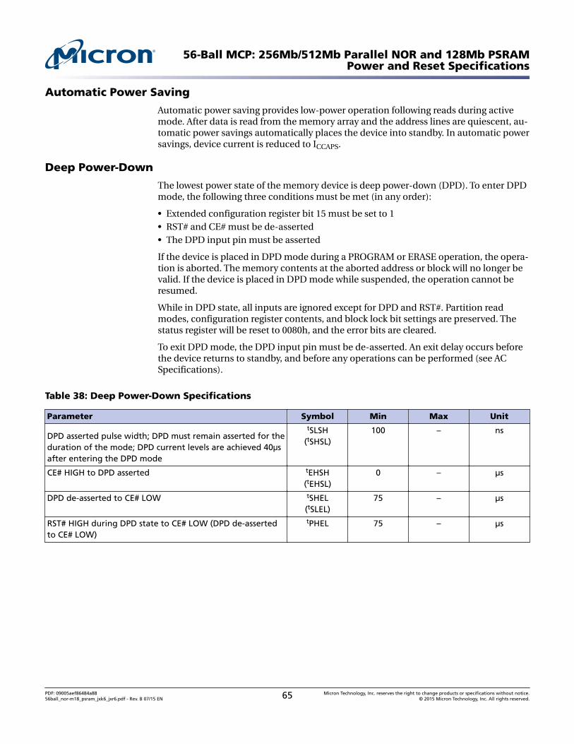
Automatic Power Saving
Automatic power saving provides low-power operation following reads during activemode. After data is read from the memory array and the address lines are quiescent, au-tomatic power savings automatically places the device into standby. In automatic powersavings, device current is reduced to ICCAPS.
Deep Power-Down
The lowest power state of the memory device is deep power-down (DPD). To enter DPDmode, the following three conditions must be met (in any order):
• Extended configuration register bit 15 must be set to 1• RST# and CE# must be de-asserted• The DPD input pin must be asserted
If the device is placed in DPD mode during a PROGRAM or ERASE operation, the opera-tion is aborted. The memory contents at the aborted address or block will no longer bevalid. If the device is placed in DPD mode while suspended, the operation cannot beresumed.
While in DPD state, all inputs are ignored except for DPD and RST#. Partition readmodes, configuration register contents, and block lock bit settings are preserved. Thestatus register will be reset to 0080h, and the error bits are cleared.
To exit DPD mode, the DPD input pin must be de-asserted. An exit delay occurs beforethe device returns to standby, and before any operations can be performed (see ACSpecifications).
Table 38: Deep Power-Down Specifications
Parameter Symbol Min Max Unit
DPD asserted pulse width; DPD must remain asserted for theduration of the mode; DPD current levels are achieved 40μsafter entering the DPD mode
tSLSH(tSHSL)
100 – ns
CE# HIGH to DPD asserted tEHSH(tEHSL)
0 – µs
DPD de-asserted to CE# LOW tSHEL(tSLEL)
75 – µs
RST# HIGH during DPD state to CE# LOW (DPD de-assertedto CE# LOW)
tPHEL 75 – µs
56-Ball MCP: 256Mb/512Mb Parallel NOR and 128Mb PSRAMPower and Reset Specifications
PDF: 09005aef86484a8856ball_nor-m18_psram_jxk6_jxr6.pdf - Rev. B 07/15 EN 65 Micron Technology, Inc. reserves the right to change products or specifications without notice.
© 2015 Micron Technology, Inc. All rights reserved.
Figure 19: Deep Power-Down Operation Timing
CE#
DPD
tSLSH
tEHSH tSHEL
RST#
Note: 1. DPD pin is LOW-true (ECR[14] = 0).
Figure 20: Reset During Deep Power-Down Operation Timing
CE#
DPD
tEHSH
tPHEL
RST#
Note: 1. DPD pin is LOW-true (ECR[14] = 0).
Power Supply Decoupling
Flash memory devices require careful power supply decoupling to prevent externaltransient noise from affecting device operations, and to prevent internallygeneratedtransient noise from affecting other devices in the system.
Ceramic chip capacitors of 0.01µF to 0.1µF should be used between all VCC, VCCQ, andVPP supply connections and system ground. These high-frequency, inherently low-in-ductance capacitors should be placed as close as possible to the device package, or onthe opposite side of the printed circuit board close to the center of the device packagefootprint.
Larger (4.7µF to 33.0µF) electrolytic or tantulum bulk capacitors should also be distrib-uted as needed throughout the system to compensate for voltage sags and surgescaused by circuit trace inductance.
Transient current magnitudes depend on the capacitive and inductive loading on thedevice’s outputs. For best signal integrity and device performance, high-speed designrules should be used when designing the printed-circuit board. Circuit-trace impedan-ces should match output-driver impedance with adequate ground-return paths. Thiswill help minimize signal reflections (overshoot/undershoot) and noise caused by high-speed signal edge rates.
56-Ball MCP: 256Mb/512Mb Parallel NOR and 128Mb PSRAMPower and Reset Specifications
PDF: 09005aef86484a8856ball_nor-m18_psram_jxk6_jxr6.pdf - Rev. B 07/15 EN 66 Micron Technology, Inc. reserves the right to change products or specifications without notice.
© 2015 Micron Technology, Inc. All rights reserved.
Electrical SpecificationsStresses greater than those listed may cause permanent damage to the device. This is astress rating only. Exposure to absolute maximum rating and operating conditions forextended periods may adversely affect reliability. Stressing the device beyond the abso-lute maximum ratings may cause permanent damage. These are stress ratings only.
Table 39: Absolute Maximum Ratings
Parameter Min Max Units Notes
Temperature under bias (TA) –40 85 °C 5
Storage temperature (TA) –65 125 °C 5
VPP voltage –2.0 11.5 V 1, 2, 3
VCC voltage –2.0 VCCQ + 2.0 V 1
Voltage on any input/output signal (except VCC, VCCQ, and VPP) –2.0 VCCQ + 2.0 V 2
VCCQ voltage –0.2 VCCQ + 2.0 V 1
VPPH time – 80 hours 3
Output short circuit current – 100 mA 4
Block PROGRAM/ERASE cycles: Main blocks 100,000 – Cycles 3
Notes: 1. Voltages shown are specified with respect to VSS. During transitions, the voltage poten-tial between VSS and input/output and supply pins may undershoot to –1.0V for periodsless than 20ns and may overshoot to VCC Q(MAX) + 1.0V for periods less than 20ns.
2. Voltages shown are specified with respect to VSS. During transitions, the voltage poten-tial between VSS and supply pins may undershoot to –2.0V for periods less than 20ns andmay overshoot to VCC (MAX) + 2.0V for periods less than 20ns.
3. Operation beyond this limit may degrade performance.4. Output shorted for no more than one second; no more than one output shorted at a
time.5. Temperature specified is ambient (TA), not case (TC).
Table 40: Operating Conditions
Symbol Parameter Min Max Units Notes
TA Operating temperature –40 85 °C 1
VCC VCC supply voltage 1.7 2.0 V
VCCQ I/O supply voltage 1.7 2.0 V
VPPL VPP voltage supply (logic level) 0.9 2.0 V
VPPH Factory programming VPP 8.5 9.5 V
Note: 1. TA = Temperature specified is ambient (TA), not case (TC).
56-Ball MCP: 256Mb/512Mb Parallel NOR and 128Mb PSRAMElectrical Specifications
PDF: 09005aef86484a8856ball_nor-m18_psram_jxk6_jxr6.pdf - Rev. B 07/15 EN 67 Micron Technology, Inc. reserves the right to change products or specifications without notice.
© 2015 Micron Technology, Inc. All rights reserved.
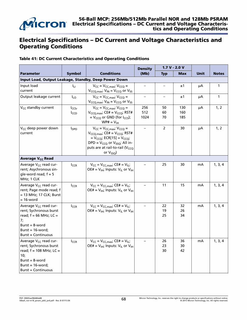
Electrical Specifications – DC Current and Voltage Characteristics andOperating Conditions
Table 41: DC Current Characteristics and Operating Conditions
Parameter Symbol ConditionsDensity
(Mb)
1.7 V - 2.0 V
Unit NotesTyp Max
Input Load, Output Leakage, Standby, Deep Power Down
Input loadcurrent
ILI VCC = VCC,max; VCCQ =VCCQ,max; VIN = VCCQ or VSS
– – ±1 µA 1
Output leakage current ILO VCC = VCC,max; VCCQ =VCCQ,max; VIN = VCCQ or VSS
– – ±1 µA 1
VCC standby current ICCS,ICCD
VCC = VCC,max; VCCQ =VCCQ,max; CE# = VCCQ; RST#= VCCQ or GND (for ICCS);
WP# = VIH
2565121024
506070
130160185
µA 1, 2
VCC deep power downcurrent
IDPD VCC = VCC,max; VCCQ =VCCQ,max; CE# = VCCQ; RST#
= VCCQ; ECR[15] = VCCQ;DPD = VCCQ or VSSQ; All in-puts are at rail-to-rail (VCCQ
or VSSQ)
– 2 30 µA 1, 2
Average VCC Read
Average VCC read cur-rent; Asychronous sin-gle-word read; f = 5MHz; 1 CLK
ICCR VCC = VCC,max; CE# = VIL;OE# = VIH; Inputs: VIL or VIH
– 25 30 mA 1, 3, 4
Average VCC read cur-rent; Page mode read; f= 13 MHz; 17 CLK; Burst= 16-word
ICCR VCC = VCC,max; CE# = VIL;OE# = VIH; Inputs: VIL or VIH
– 11 15 mA 1, 3, 4
Average VCC read cur-rent; Sychronous burstread; f = 66 MHz; LC =7;Burst = 8-wordBurst = 16-word;Burst = Continuous
ICCR VCC = VCC,max; CE# = VIL;OE# = VIH; Inputs: VIL or VIH
– 221925
322634
mA 1, 3, 4
Average VCC read cur-rent; Sychronous burstread; f = 108 MHz; LC =10;Burst = 8-wordBurst = 16-word;Burst = Continuous
ICCR VCC = VCC,max; CE# = VIL;OE# = VIH; Inputs: VIL or VIH
– 262330
363042
mA 1, 3, 4
56-Ball MCP: 256Mb/512Mb Parallel NOR and 128Mb PSRAMElectrical Specifications – DC Current and Voltage Characteris-
tics and Operating Conditions
PDF: 09005aef86484a8856ball_nor-m18_psram_jxk6_jxr6.pdf - Rev. B 07/15 EN 68 Micron Technology, Inc. reserves the right to change products or specifications without notice.
© 2015 Micron Technology, Inc. All rights reserved.
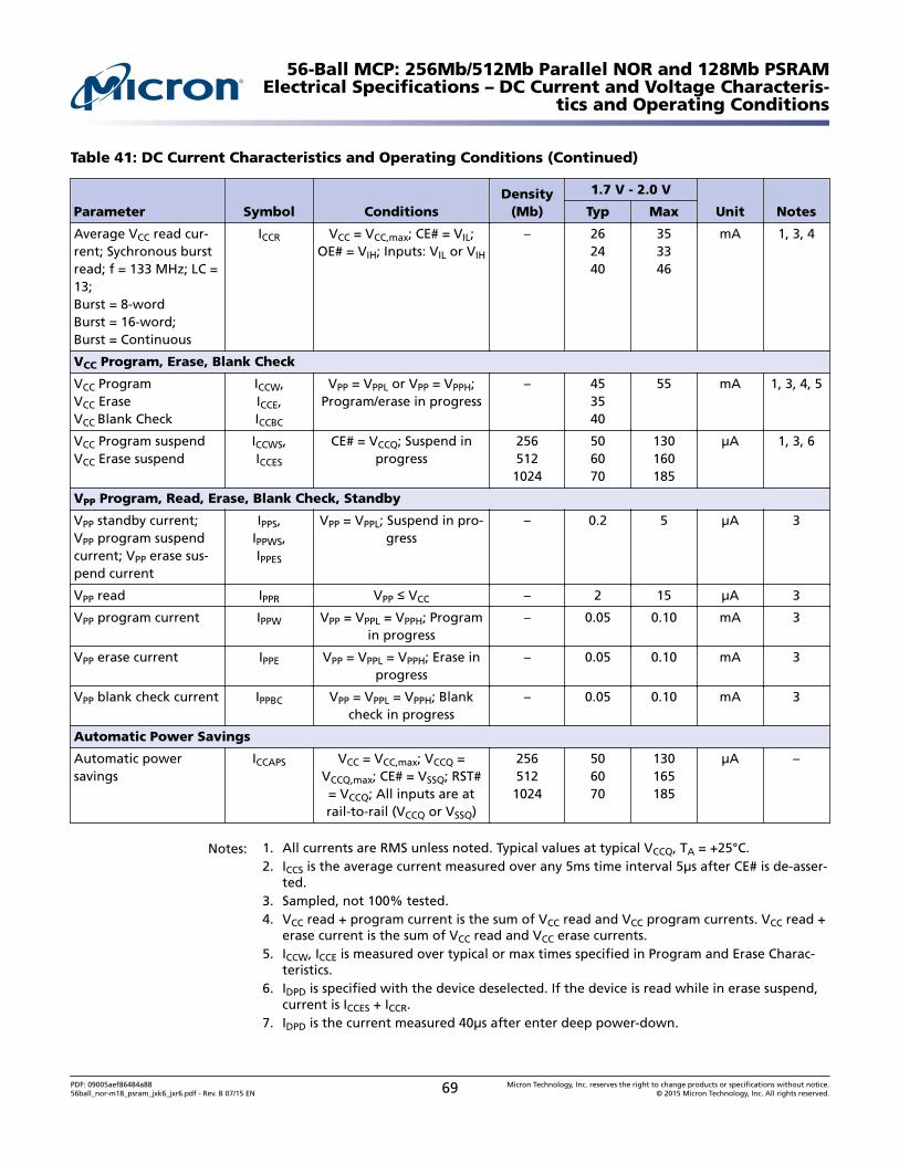
Table 41: DC Current Characteristics and Operating Conditions (Continued)
Parameter Symbol ConditionsDensity
(Mb)
1.7 V - 2.0 V
Unit NotesTyp Max
Average VCC read cur-rent; Sychronous burstread; f = 133 MHz; LC =13;Burst = 8-wordBurst = 16-word;Burst = Continuous
ICCR VCC = VCC,max; CE# = VIL;OE# = VIH; Inputs: VIL or VIH
– 262440
353346
mA 1, 3, 4
VCC Program, Erase, Blank Check
VCC ProgramVCC EraseVCC Blank Check
ICCW,ICCE,ICCBC
VPP = VPPL or VPP = VPPH;Program/erase in progress
– 453540
55 mA 1, 3, 4, 5
VCC Program suspendVCC Erase suspend
ICCWS,ICCES
CE# = VCCQ; Suspend inprogress
2565121024
506070
130160185
µA 1, 3, 6
VPP Program, Read, Erase, Blank Check, Standby
VPP standby current;VPP program suspendcurrent; VPP erase sus-pend current
IPPS,IPPWS,IPPES
VPP = VPPL; Suspend in pro-gress
– 0.2 5 µA 3
VPP read IPPR VPP ≤ VCC – 2 15 µA 3
VPP program current IPPW VPP = VPPL = VPPH; Programin progress
– 0.05 0.10 mA 3
VPP erase current IPPE VPP = VPPL = VPPH; Erase inprogress
– 0.05 0.10 mA 3
VPP blank check current IPPBC VPP = VPPL = VPPH; Blankcheck in progress
– 0.05 0.10 mA 3
Automatic Power Savings
Automatic powersavings
ICCAPS VCC = VCC,max; VCCQ =VCCQ,max; CE# = VSSQ; RST#= VCCQ; All inputs are atrail-to-rail (VCCQ or VSSQ)
256512
1024
506070
130165185
µA –
Notes: 1. All currents are RMS unless noted. Typical values at typical VCCQ, TA = +25°C.2. ICCS is the average current measured over any 5ms time interval 5µs after CE# is de-asser-
ted.3. Sampled, not 100% tested.4. VCC read + program current is the sum of VCC read and VCC program currents. VCC read +
erase current is the sum of VCC read and VCC erase currents.5. ICCW, ICCE is measured over typical or max times specified in Program and Erase Charac-
teristics.6. IDPD is specified with the device deselected. If the device is read while in erase suspend,
current is ICCES + ICCR.7. IDPD is the current measured 40µs after enter deep power-down.
56-Ball MCP: 256Mb/512Mb Parallel NOR and 128Mb PSRAMElectrical Specifications – DC Current and Voltage Characteris-
tics and Operating Conditions
PDF: 09005aef86484a8856ball_nor-m18_psram_jxk6_jxr6.pdf - Rev. B 07/15 EN 69 Micron Technology, Inc. reserves the right to change products or specifications without notice.
© 2015 Micron Technology, Inc. All rights reserved.
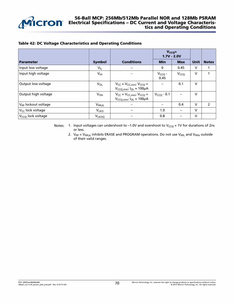
Table 42: DC Voltage Characteristics and Operating Conditions
Parameter Symbol Conditions
VCCQ=1.7V - 2.0V
Unit NotesMin Max
Input low voltage VIL – 0 0.45 V 1
Input high voltage VIH – VCCQ -0.45
VCCQ V 1
Output low voltage VOL VCC = VCC,min; VCCQ =VCCQ,min; IOL = 100µA
– 0.1 V
Output high voltage VOH VCC = VCC,min; VCCQ =VCCQ,min; IOL = 100µA
VCCQ - 0.1 – V
VPP lockout voltage VPPLK – – 0.4 V 2
VCC lock voltage VLKO – 1.0 – V
VCCQ lock voltage VLKOQ – 0.8 – V
Notes: 1. Input voltages can undershoot to –1.0V and overshoot to VCCQ + 1V for durations of 2nsor less.
2. VPP < VPPLK inhibits ERASE and PROGRAM operations. Do not use VPPL and VPPH outsideof their valid ranges.
56-Ball MCP: 256Mb/512Mb Parallel NOR and 128Mb PSRAMElectrical Specifications – DC Current and Voltage Characteris-
tics and Operating Conditions
PDF: 09005aef86484a8856ball_nor-m18_psram_jxk6_jxr6.pdf - Rev. B 07/15 EN 70 Micron Technology, Inc. reserves the right to change products or specifications without notice.
© 2015 Micron Technology, Inc. All rights reserved.
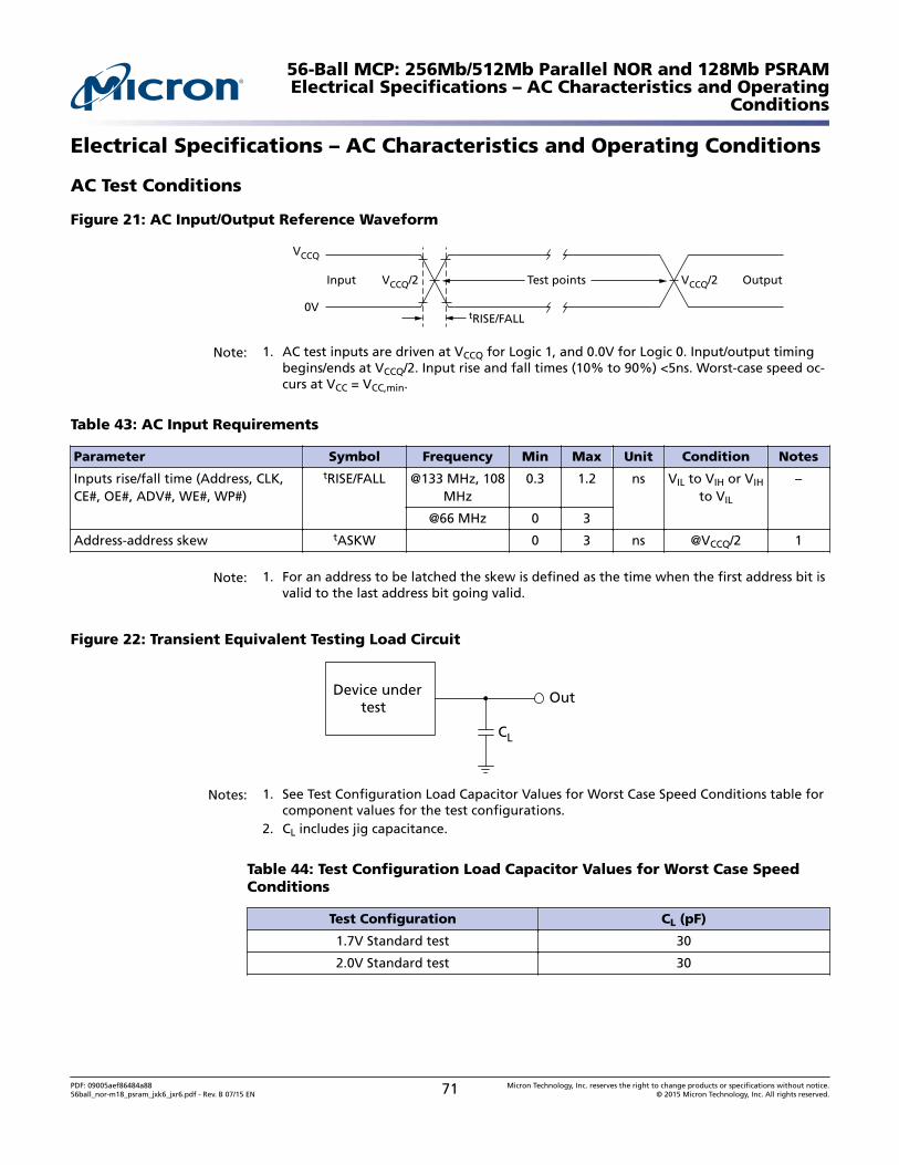
Electrical Specifications – AC Characteristics and Operating Conditions
AC Test Conditions
Figure 21: AC Input/Output Reference Waveform
tRISE/FALL
VCCQ/2Input VCCQ/2 Output
VCCQ
0V
Test points
Note: 1. AC test inputs are driven at VCCQ for Logic 1, and 0.0V for Logic 0. Input/output timingbegins/ends at VCCQ/2. Input rise and fall times (10% to 90%) <5ns. Worst-case speed oc-curs at VCC = VCC,min.
Table 43: AC Input Requirements
Parameter Symbol Frequency Min Max Unit Condition Notes
Inputs rise/fall time (Address, CLK,CE#, OE#, ADV#, WE#, WP#)
tRISE/FALL @133 MHz, 108MHz
0.3 1.2 ns VIL to VIH or VIH
to VIL
–
@66 MHz 0 3
Address-address skew tASKW 0 3 ns @VCCQ/2 1
Note: 1. For an address to be latched the skew is defined as the time when the first address bit isvalid to the last address bit going valid.
Figure 22: Transient Equivalent Testing Load Circuit
Device undertest
Out
CL
Notes: 1. See Test Configuration Load Capacitor Values for Worst Case Speed Conditions table forcomponent values for the test configurations.
2. CL includes jig capacitance.
Table 44: Test Configuration Load Capacitor Values for Worst Case SpeedConditions
Test Configuration CL (pF)
1.7V Standard test 30
2.0V Standard test 30
56-Ball MCP: 256Mb/512Mb Parallel NOR and 128Mb PSRAMElectrical Specifications – AC Characteristics and Operating
Conditions
PDF: 09005aef86484a8856ball_nor-m18_psram_jxk6_jxr6.pdf - Rev. B 07/15 EN 71 Micron Technology, Inc. reserves the right to change products or specifications without notice.
© 2015 Micron Technology, Inc. All rights reserved.
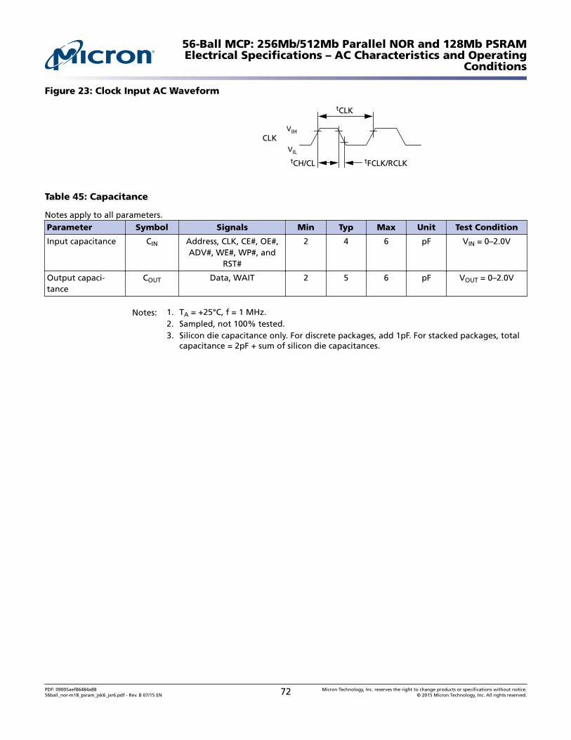
Figure 23: Clock Input AC Waveform
tFCLK/RCLK
CLK
tCH/CL
VIH
VIL
tCLK
Table 45: Capacitance
Notes apply to all parameters.Parameter Symbol Signals Min Typ Max Unit Test Condition
Input capacitance CIN Address, CLK, CE#, OE#,ADV#, WE#, WP#, and
RST#
2 4 6 pF VIN = 0–2.0V
Output capaci-tance
COUT Data, WAIT 2 5 6 pF VOUT = 0–2.0V
Notes: 1. TA = +25°C, f = 1 MHz.2. Sampled, not 100% tested.3. Silicon die capacitance only. For discrete packages, add 1pF. For stacked packages, total
capacitance = 2pF + sum of silicon die capacitances.
56-Ball MCP: 256Mb/512Mb Parallel NOR and 128Mb PSRAMElectrical Specifications – AC Characteristics and Operating
Conditions
PDF: 09005aef86484a8856ball_nor-m18_psram_jxk6_jxr6.pdf - Rev. B 07/15 EN 72 Micron Technology, Inc. reserves the right to change products or specifications without notice.
© 2015 Micron Technology, Inc. All rights reserved.
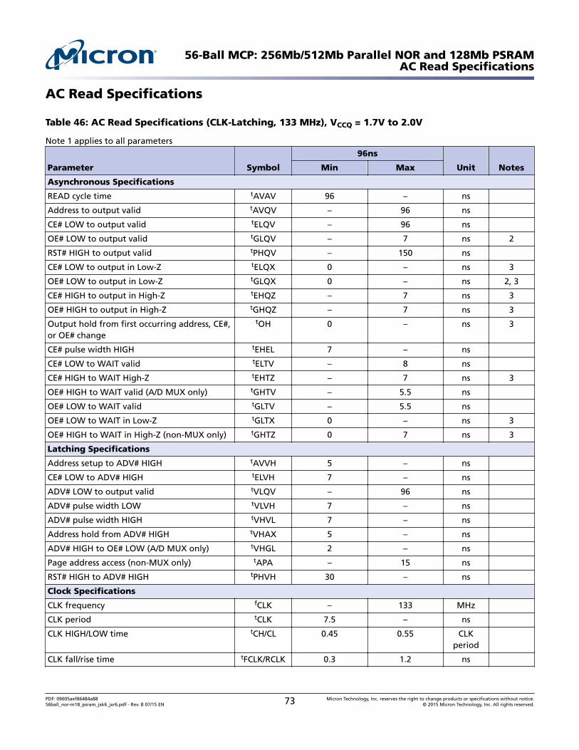
AC Read Specifications
Table 46: AC Read Specifications (CLK-Latching, 133 MHz), VCCQ = 1.7V to 2.0V
Note 1 applies to all parameters
Parameter Symbol
96ns
Unit NotesMin Max
Asynchronous Specifications
READ cycle time tAVAV 96 – ns
Address to output valid tAVQV – 96 ns
CE# LOW to output valid tELQV – 96 ns
OE# LOW to output valid tGLQV – 7 ns 2
RST# HIGH to output valid tPHQV – 150 ns
CE# LOW to output in Low-Z tELQX 0 – ns 3
OE# LOW to output in Low-Z tGLQX 0 – ns 2, 3
CE# HIGH to output in High-Z tEHQZ – 7 ns 3
OE# HIGH to output in High-Z tGHQZ – 7 ns 3
Output hold from first occurring address, CE#,or OE# change
tOH 0 – ns 3
CE# pulse width HIGH tEHEL 7 – ns
CE# LOW to WAIT valid tELTV – 8 ns
CE# HIGH to WAIT High-Z tEHTZ – 7 ns 3
OE# HIGH to WAIT valid (A/D MUX only) tGHTV – 5.5 ns
OE# LOW to WAIT valid tGLTV – 5.5 ns
OE# LOW to WAIT in Low-Z tGLTX 0 – ns 3
OE# HIGH to WAIT in High-Z (non-MUX only) tGHTZ 0 7 ns 3
Latching Specifications
Address setup to ADV# HIGH tAVVH 5 – ns
CE# LOW to ADV# HIGH tELVH 7 – ns
ADV# LOW to output valid tVLQV – 96 ns
ADV# pulse width LOW tVLVH 7 – ns
ADV# pulse width HIGH tVHVL 7 – ns
Address hold from ADV# HIGH tVHAX 5 – ns
ADV# HIGH to OE# LOW (A/D MUX only) tVHGL 2 – ns
Page address access (non-MUX only) tAPA – 15 ns
RST# HIGH to ADV# HIGH tPHVH 30 – ns
Clock Specifications
CLK frequency fCLK – 133 MHz
CLK period tCLK 7.5 – ns
CLK HIGH/LOW time tCH/CL 0.45 0.55 CLKperiod
CLK fall/rise time tFCLK/RCLK 0.3 1.2 ns
56-Ball MCP: 256Mb/512Mb Parallel NOR and 128Mb PSRAMAC Read Specifications
PDF: 09005aef86484a8856ball_nor-m18_psram_jxk6_jxr6.pdf - Rev. B 07/15 EN 73 Micron Technology, Inc. reserves the right to change products or specifications without notice.
© 2015 Micron Technology, Inc. All rights reserved.
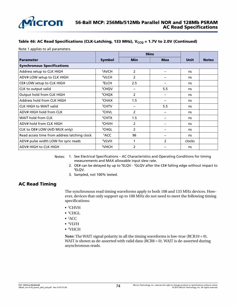
Table 46: AC Read Specifications (CLK-Latching, 133 MHz), VCCQ = 1.7V to 2.0V (Continued)
Note 1 applies to all parameters
Parameter Symbol
96ns
Unit NotesMin Max
Synchronous Specifications
Address setup to CLK HIGH tAVCH 2 – ns
ADV# LOW setup to CLK HIGH tVLCH 2 – ns
CE# LOW setup to CLK HIGH tELCH 2.5 – ns
CLK to output valid tCHQV – 5.5 ns
Output hold from CLK HIGH tCHQX 2 – ns
Address hold from CLK HIGH tCHAX 1.5 – ns
CLK HIGH to WAIT valid tCHTV – 5.5 ns
ADV# HIGH hold from CLK tCHVL 2 – ns
WAIT hold from CLK tCHTX 1.5 – ns
ADV# hold from CLK HIGH tCHVH 2 – ns
CLK to OE# LOW (A/D MUX only) tCHGL 2 – ns
Read access time from address latching clock tACC 96 – ns
ADV# pulse width LOW for sync reads tVLVH 1 2 clocks
ADV# HIGH to CLK HIGH tVHCH 2 – ns
Notes: 1. See Electrical Specifications – AC Characteristics and Operating Conditions for timingmeasurements and MAX allowable input slew rate.
2. OE# can be delayed by up to tELQV - tGLQV after the CE# falling edge without impact totELQV.
3. Sampled, not 100% tested.
AC Read Timing
The synchronous read timing waveforms apply to both 108 and 133 MHz devices. How-ever, devices that only support up to 108 MHz do not need to meet the following timingspecifications:
• tCHVH• tCHGL• tACC• tVLVH• tVHCH
Note: The WAIT signal polarity in all the timing waveforms is low-true (RCR10 = 0).WAIT is shown as de-asserted with valid data (RCR8 = 0). WAIT is de-asserted duringasynchronous reads.
56-Ball MCP: 256Mb/512Mb Parallel NOR and 128Mb PSRAMAC Read Specifications
PDF: 09005aef86484a8856ball_nor-m18_psram_jxk6_jxr6.pdf - Rev. B 07/15 EN 74 Micron Technology, Inc. reserves the right to change products or specifications without notice.
© 2015 Micron Technology, Inc. All rights reserved.
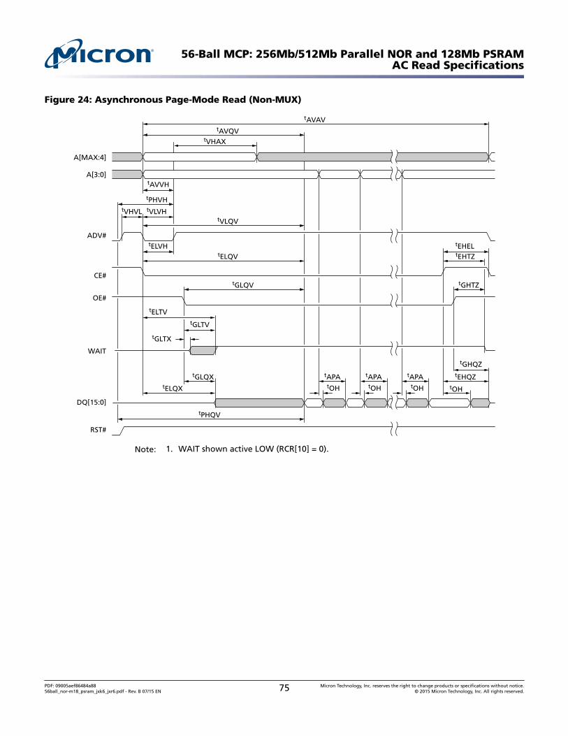
Figure 24: Asynchronous Page-Mode Read (Non-MUX)
A[MAX:4]
A[3:0]
ADV#
tAVAVtAVQV
tVLQV
tVHAX
tAVVH
tPHVHtVLVHtVHVL
CE#
OE#
WAIT
DQ[15:0]tPHQV
tGHQZtEHQZ
tOH
tAPAtGLQXtELQX
tELVH
tELTVtGLTV
tGLTX
tAPAtOHtOH
tAPAtOH
RST#
tELQV
tEHELtEHTZ
tGLQV tGHTZ
Note: 1. WAIT shown active LOW (RCR[10] = 0).
56-Ball MCP: 256Mb/512Mb Parallel NOR and 128Mb PSRAMAC Read Specifications
PDF: 09005aef86484a8856ball_nor-m18_psram_jxk6_jxr6.pdf - Rev. B 07/15 EN 75 Micron Technology, Inc. reserves the right to change products or specifications without notice.
© 2015 Micron Technology, Inc. All rights reserved.
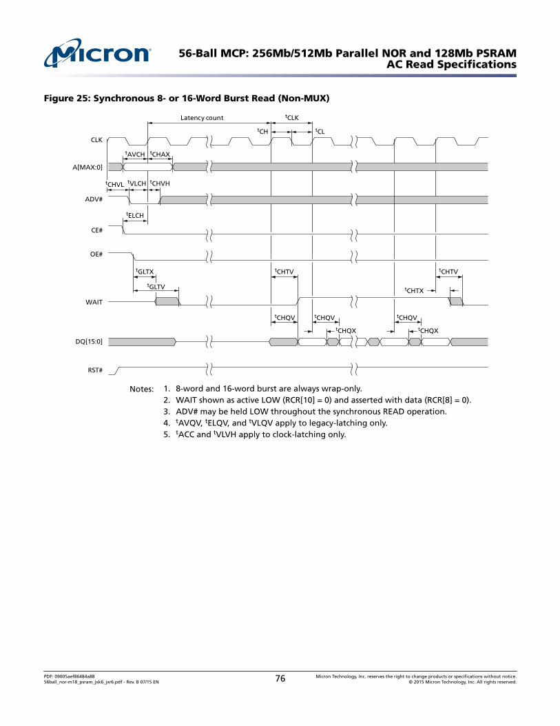
Figure 25: Synchronous 8- or 16-Word Burst Read (Non-MUX)
A[MAX:0]
CLK
ADV#
Latency count
CE#
OE#
WAIT
DQ[15:0]
tCHVHtVLCH
tAVCH tCHAX
tCHTV
tCHQV
tELCH
tGLTX
tCHQV
tCHTX
tCHQX
tCLK
tCH tCL
RST#
tCHQV
tCHQX
tCHTV
tGLTV
tCHVL
Notes: 1. 8-word and 16-word burst are always wrap-only.2. WAIT shown as active LOW (RCR[10] = 0) and asserted with data (RCR[8] = 0).3. ADV# may be held LOW throughout the synchronous READ operation.4. tAVQV, tELQV, and tVLQV apply to legacy-latching only.5. tACC and tVLVH apply to clock-latching only.
56-Ball MCP: 256Mb/512Mb Parallel NOR and 128Mb PSRAMAC Read Specifications
PDF: 09005aef86484a8856ball_nor-m18_psram_jxk6_jxr6.pdf - Rev. B 07/15 EN 76 Micron Technology, Inc. reserves the right to change products or specifications without notice.
© 2015 Micron Technology, Inc. All rights reserved.
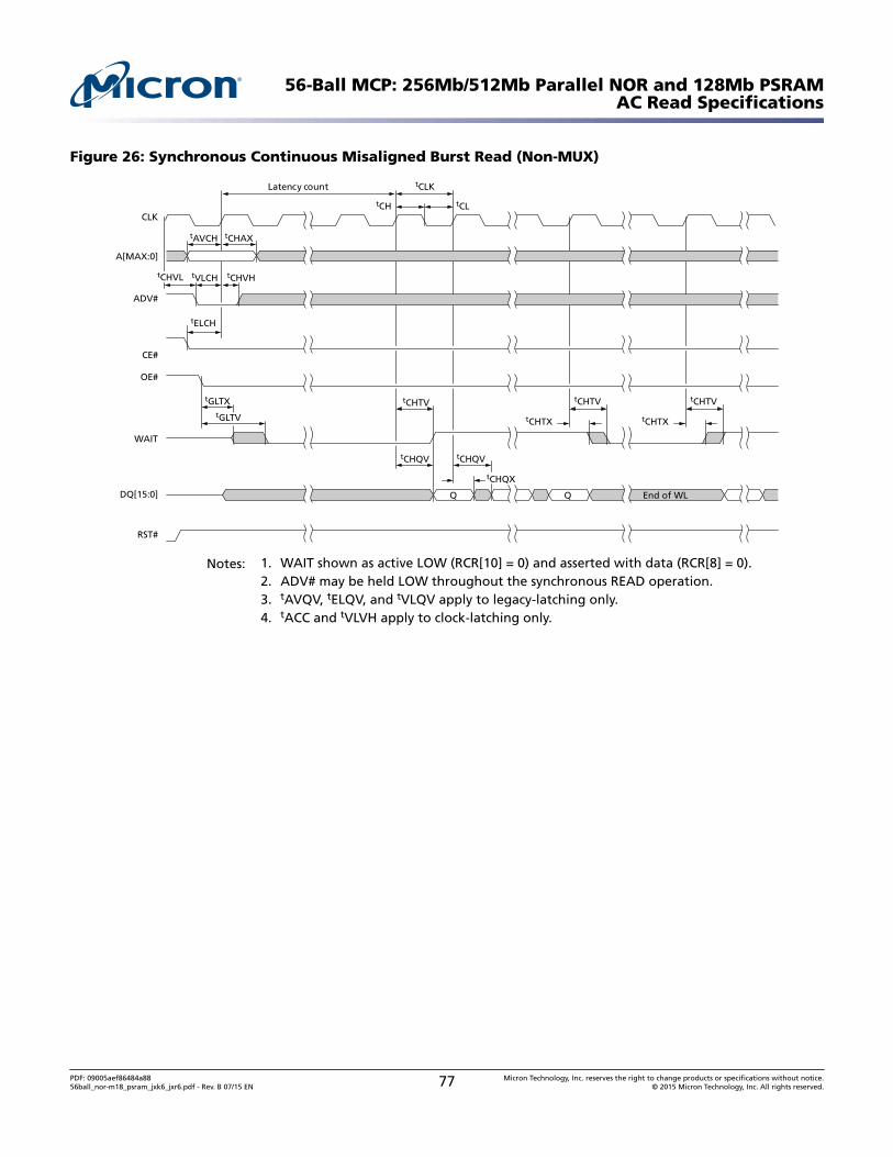
Figure 26: Synchronous Continuous Misaligned Burst Read (Non-MUX)
A[MAX:0]
CLK
ADV#
Latency count
CE#
OE#
WAIT
DQ[15:0]
tCHVHtVLCH
tAVCH tCHAX
tCHTVtCHTV
tCHQV
tELCH
tGLTX
tCHQV
tCHTX
tCHQX
tCLK
tCH tCL
RST#
tCHTV
tCHTX
tCHVL
tGLTV
End of WLQ Q
Notes: 1. WAIT shown as active LOW (RCR[10] = 0) and asserted with data (RCR[8] = 0).2. ADV# may be held LOW throughout the synchronous READ operation.3. tAVQV, tELQV, and tVLQV apply to legacy-latching only.4. tACC and tVLVH apply to clock-latching only.
56-Ball MCP: 256Mb/512Mb Parallel NOR and 128Mb PSRAMAC Read Specifications
PDF: 09005aef86484a8856ball_nor-m18_psram_jxk6_jxr6.pdf - Rev. B 07/15 EN 77 Micron Technology, Inc. reserves the right to change products or specifications without notice.
© 2015 Micron Technology, Inc. All rights reserved.
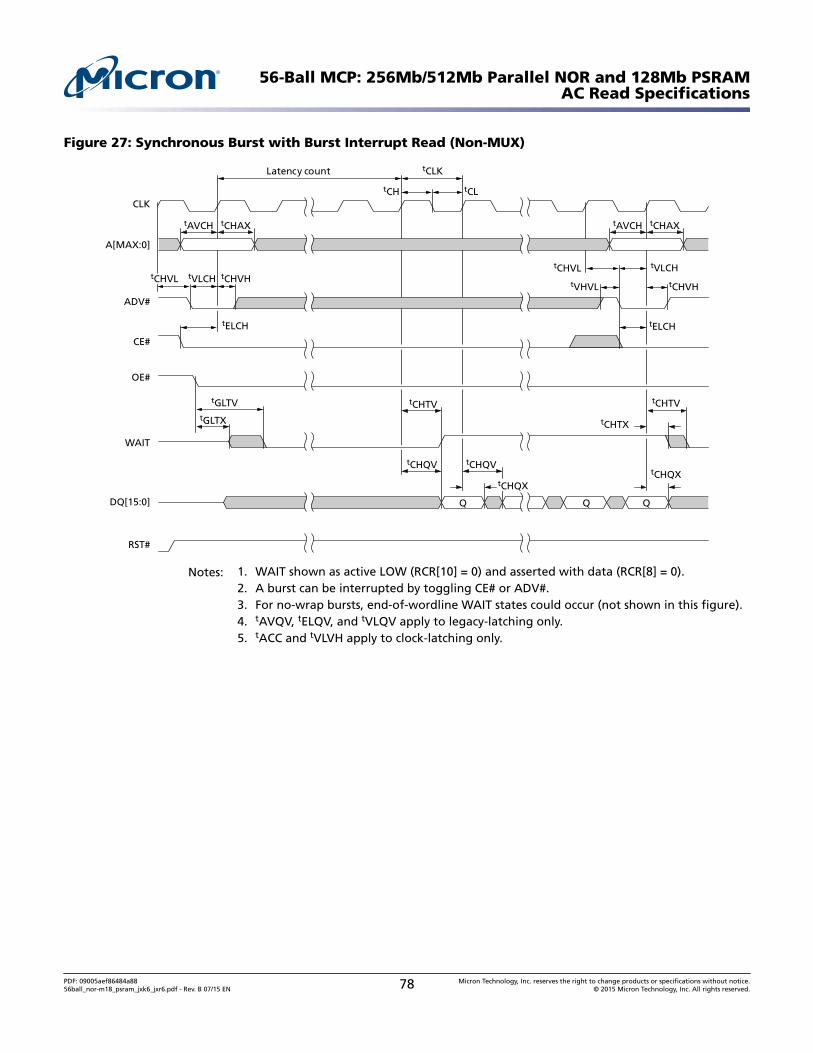
Figure 27: Synchronous Burst with Burst Interrupt Read (Non-MUX)
tCL
A[MAX:0]
CLK
ADV#
Latency count
CE#
OE#
WAIT
DQ[15:0]
tCHVHtVLCH
tAVCH tCHAX tAVCH tCHAX
tCHTVtCHTV
tCHQV
tELCH tELCH
tGLTX
tCHQV
tCHTX
tCHQX
tCLK
tCH
RST#
tCHQX
tGLTV
tCHVLtCHVHtVHVL
tVLCHtCHVL
Q Q Q
Notes: 1. WAIT shown as active LOW (RCR[10] = 0) and asserted with data (RCR[8] = 0).2. A burst can be interrupted by toggling CE# or ADV#.3. For no-wrap bursts, end-of-wordline WAIT states could occur (not shown in this figure).4. tAVQV, tELQV, and tVLQV apply to legacy-latching only.5. tACC and tVLVH apply to clock-latching only.
56-Ball MCP: 256Mb/512Mb Parallel NOR and 128Mb PSRAMAC Read Specifications
PDF: 09005aef86484a8856ball_nor-m18_psram_jxk6_jxr6.pdf - Rev. B 07/15 EN 78 Micron Technology, Inc. reserves the right to change products or specifications without notice.
© 2015 Micron Technology, Inc. All rights reserved.
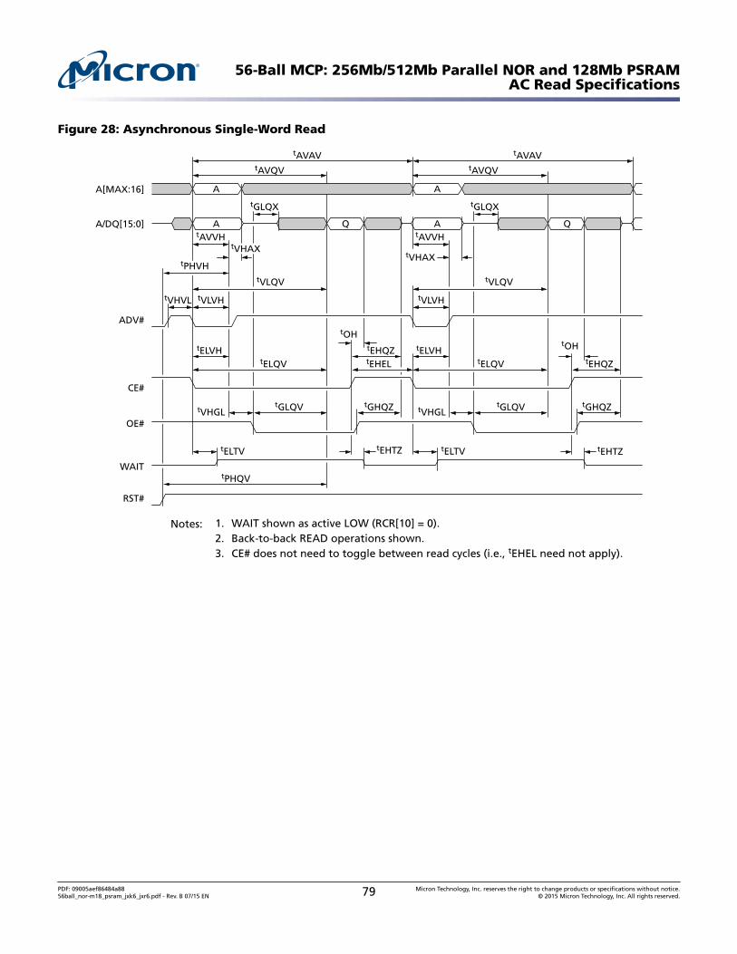
Figure 28: Asynchronous Single-Word Read
A[MAX:16]
A/DQ[15:0]
ADV#
tAVAVtAVQV
tAVVH
tVLVHtVHVL
CE#
OE#
WAITtPHQV
tVLQV
tVLVH
tVLQV
tELVH
tGLQXtGLQX
tEHTZtEHTZ tELTVtELTV
tAVAVtAVQV
RST#
tELQV
tEHQZ tELVHtEHEL tELQV
tOHtOH
tEHQZ
tGLQV tGHQZ tVHGLtVHGLtGHQZtGLQV
A A
A Q QA
tVHAX
tAVVH
tVHAXtPHVH
Notes: 1. WAIT shown as active LOW (RCR[10] = 0).2. Back-to-back READ operations shown.3. CE# does not need to toggle between read cycles (i.e., tEHEL need not apply).
56-Ball MCP: 256Mb/512Mb Parallel NOR and 128Mb PSRAMAC Read Specifications
PDF: 09005aef86484a8856ball_nor-m18_psram_jxk6_jxr6.pdf - Rev. B 07/15 EN 79 Micron Technology, Inc. reserves the right to change products or specifications without notice.
© 2015 Micron Technology, Inc. All rights reserved.
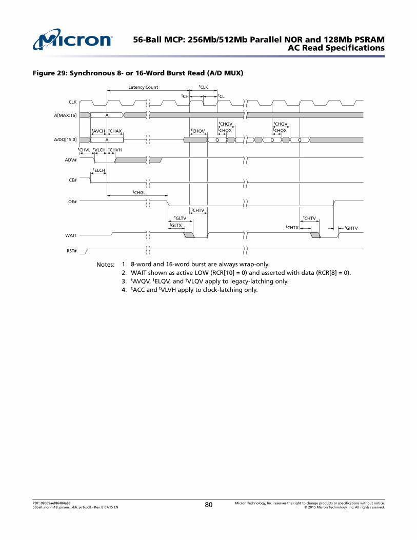
Figure 29: Synchronous 8- or 16-Word Burst Read (A/D MUX)
A[MAX:16]
CLK
ADV#
Latency Count
CE#
OE#
WAIT
A/DQ[15:0]
tCHVH
tAVCH tCHAX tCHQV
tCHQV
tGLTV
tELCH
tCHGL
tCHTV
tCLK
tCH tCL
RST#
tVLCH
tGLTX
tCHVL
Q
A
A
tCHQX
tCHQV
Q Q
tCHQX
tCHTV
tCHTX tGHTV
Notes: 1. 8-word and 16-word burst are always wrap-only.2. WAIT shown as active LOW (RCR[10] = 0) and asserted with data (RCR[8] = 0).3. tAVQV, tELQV, and tVLQV apply to legacy-latching only.4. tACC and tVLVH apply to clock-latching only.
56-Ball MCP: 256Mb/512Mb Parallel NOR and 128Mb PSRAMAC Read Specifications
PDF: 09005aef86484a8856ball_nor-m18_psram_jxk6_jxr6.pdf - Rev. B 07/15 EN 80 Micron Technology, Inc. reserves the right to change products or specifications without notice.
© 2015 Micron Technology, Inc. All rights reserved.
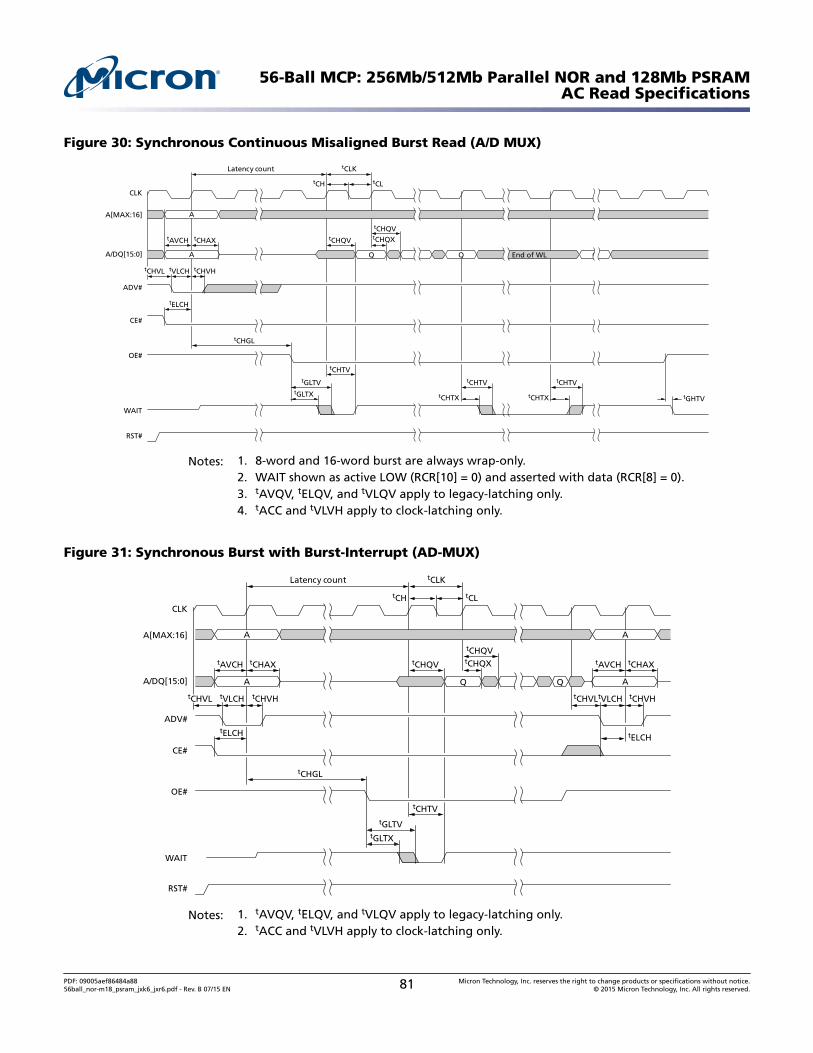
Figure 30: Synchronous Continuous Misaligned Burst Read (A/D MUX)
A[MAX:16]
CLK
ADV#
Latency count
CE#
OE#
WAIT
A/DQ[15:0]
tCHVH
tAVCH tCHAX tCHQV
tCHQV
tGLTV
tELCH
tCHGL
tCHTV
tCLK
tCH tCL
RST#
tVLCH
tGLTX
tCHVL
Q
A
A
tCHQX
Q End of WL Q
tCHTV
tCHTX tGHTV
tCHTV
tCHTX
Notes: 1. 8-word and 16-word burst are always wrap-only.2. WAIT shown as active LOW (RCR[10] = 0) and asserted with data (RCR[8] = 0).3. tAVQV, tELQV, and tVLQV apply to legacy-latching only.4. tACC and tVLVH apply to clock-latching only.
Figure 31: Synchronous Burst with Burst-Interrupt (AD-MUX)
A[MAX:16]
CLK
ADV#
Latency count
CE#
OE#
WAIT
A/DQ[15:0]
tCHVHtVLCH
tAVCH tCHAX tCHQV
tCHQVtAVCH tCHAX
tGLTV
tELCH
tCHGL
tCHTV
tCLK
tCH tCL
RST#
tGLTX
tCHVL tCHVHtVLCHtCHVL
Q Q
A
A
A
tCHQX
A
tELCH
Notes: 1. tAVQV, tELQV, and tVLQV apply to legacy-latching only.2. tACC and tVLVH apply to clock-latching only.
56-Ball MCP: 256Mb/512Mb Parallel NOR and 128Mb PSRAMAC Read Specifications
PDF: 09005aef86484a8856ball_nor-m18_psram_jxk6_jxr6.pdf - Rev. B 07/15 EN 81 Micron Technology, Inc. reserves the right to change products or specifications without notice.
© 2015 Micron Technology, Inc. All rights reserved.
3. A burst can be interrupted by toggling CE# or ADV#.
56-Ball MCP: 256Mb/512Mb Parallel NOR and 128Mb PSRAMAC Read Specifications
PDF: 09005aef86484a8856ball_nor-m18_psram_jxk6_jxr6.pdf - Rev. B 07/15 EN 82 Micron Technology, Inc. reserves the right to change products or specifications without notice.
© 2015 Micron Technology, Inc. All rights reserved.
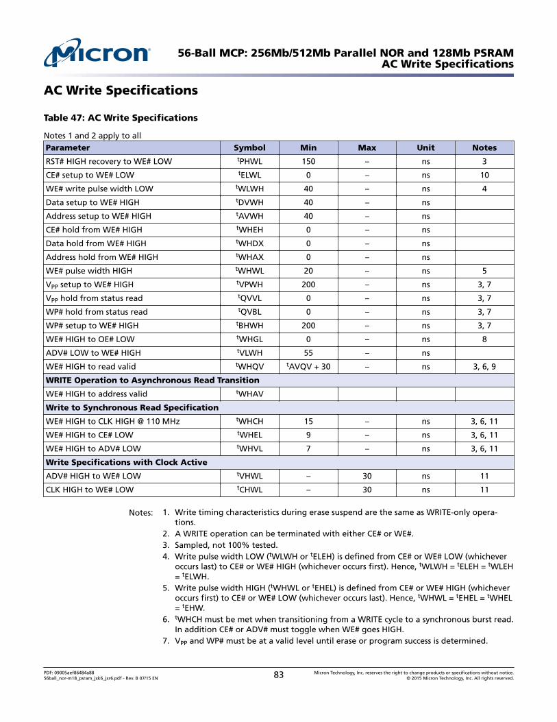
AC Write Specifications
Table 47: AC Write Specifications
Notes 1 and 2 apply to allParameter Symbol Min Max Unit Notes
RST# HIGH recovery to WE# LOW tPHWL 150 – ns 3
CE# setup to WE# LOW tELWL 0 – ns 10
WE# write pulse width LOW tWLWH 40 – ns 4
Data setup to WE# HIGH tDVWH 40 – ns
Address setup to WE# HIGH tAVWH 40 – ns
CE# hold from WE# HIGH tWHEH 0 – ns
Data hold from WE# HIGH tWHDX 0 – ns
Address hold from WE# HIGH tWHAX 0 – ns
WE# pulse width HIGH tWHWL 20 – ns 5
VPP setup to WE# HIGH tVPWH 200 – ns 3, 7
VPP hold from status read tQVVL 0 – ns 3, 7
WP# hold from status read tQVBL 0 – ns 3, 7
WP# setup to WE# HIGH tBHWH 200 – ns 3, 7
WE# HIGH to OE# LOW tWHGL 0 – ns 8
ADV# LOW to WE# HIGH tVLWH 55 – ns
WE# HIGH to read valid tWHQV tAVQV + 30 – ns 3, 6, 9
WRITE Operation to Asynchronous Read Transition
WE# HIGH to address valid tWHAV
Write to Synchronous Read Specification
WE# HIGH to CLK HIGH @ 110 MHz tWHCH 15 – ns 3, 6, 11
WE# HIGH to CE# LOW tWHEL 9 – ns 3, 6, 11
WE# HIGH to ADV# LOW tWHVL 7 – ns 3, 6, 11
Write Specifications with Clock Active
ADV# HIGH to WE# LOW tVHWL – 30 ns 11
CLK HIGH to WE# LOW tCHWL – 30 ns 11
Notes: 1. Write timing characteristics during erase suspend are the same as WRITE-only opera-tions.
2. A WRITE operation can be terminated with either CE# or WE#.3. Sampled, not 100% tested.4. Write pulse width LOW (tWLWH or tELEH) is defined from CE# or WE# LOW (whichever
occurs last) to CE# or WE# HIGH (whichever occurs first). Hence, tWLWH = tELEH = tWLEH= tELWH.
5. Write pulse width HIGH (tWHWL or tEHEL) is defined from CE# or WE# HIGH (whicheveroccurs first) to CE# or WE# LOW (whichever occurs last). Hence, tWHWL = tEHEL = tWHEL= tEHW.
6. tWHCH must be met when transitioning from a WRITE cycle to a synchronous burst read.In addition CE# or ADV# must toggle when WE# goes HIGH.
7. VPP and WP# must be at a valid level until erase or program success is determined.
56-Ball MCP: 256Mb/512Mb Parallel NOR and 128Mb PSRAMAC Write Specifications
PDF: 09005aef86484a8856ball_nor-m18_psram_jxk6_jxr6.pdf - Rev. B 07/15 EN 83 Micron Technology, Inc. reserves the right to change products or specifications without notice.
© 2015 Micron Technology, Inc. All rights reserved.
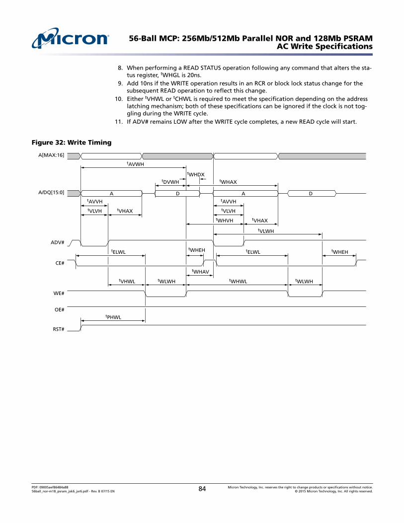
8. When performing a READ STATUS operation following any command that alters the sta-tus register, tWHGL is 20ns.
9. Add 10ns if the WRITE operation results in an RCR or block lock status change for thesubsequent READ operation to reflect this change.
10. Either tVHWL or tCHWL is required to meet the specification depending on the addresslatching mechanism; both of these specifications can be ignored if the clock is not tog-gling during the WRITE cycle.
11. If ADV# remains LOW after the WRITE cycle completes, a new READ cycle will start.
Figure 32: Write Timing
AD
tWHEH
tAVWH
tWHDX
A[MAX:16]
A/DQ[15:0]
ADV#
CE#
OE#
RST#
WE#
tVHAX
tAVVH
tVLVH tVLVH
tAVVH
tELWL
tPHWL
tELWL
tWHWLtWLWHtVHWL tWLWH
tVHAX
tWHAXtDVWH
tWHAV
tWHEH
A
tWHVH
D
tVLWH
56-Ball MCP: 256Mb/512Mb Parallel NOR and 128Mb PSRAMAC Write Specifications
PDF: 09005aef86484a8856ball_nor-m18_psram_jxk6_jxr6.pdf - Rev. B 07/15 EN 84 Micron Technology, Inc. reserves the right to change products or specifications without notice.
© 2015 Micron Technology, Inc. All rights reserved.
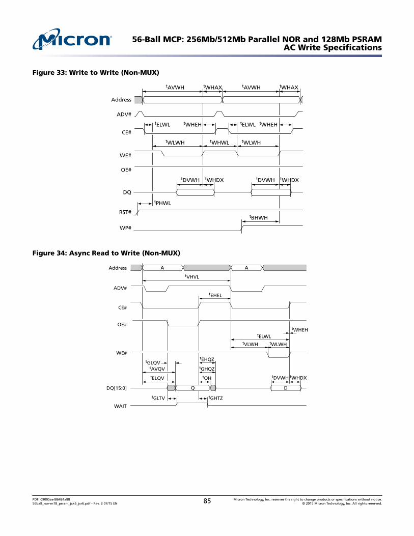
Figure 33: Write to Write (Non-MUX)
tAVWH
tELWL tELWLtWHEH
Address
ADV#
CE#
WE#
OE#
DQ
RST#
WP#
tDVWH
tPHWL
tDVWH
tBHWH
tWHDX tWHDX
tWHEH
tAVWHtWHAX
tWLWH tWLWHtWHWL
tWHAX
Figure 34: Async Read to Write (Non-MUX)
Address
ADV#
CE#
OE#
WE#
WAIT
tVHVL
tGLTV tGHTZ
tGLQV
tOH tDVWH tWHDX
tGHQZ
tELQV
tAVQV
tEHQZ
tEHEL
tWHEH
tWLWHtVLWH
tELWL
A A
DQ[15:0] Q D
56-Ball MCP: 256Mb/512Mb Parallel NOR and 128Mb PSRAMAC Write Specifications
PDF: 09005aef86484a8856ball_nor-m18_psram_jxk6_jxr6.pdf - Rev. B 07/15 EN 85 Micron Technology, Inc. reserves the right to change products or specifications without notice.
© 2015 Micron Technology, Inc. All rights reserved.
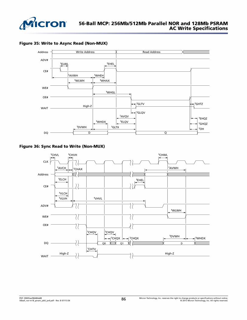
Figure 35: Write to Async Read (Non-MUX)
Address
ADV#
CE#
WE#
OE#
WAIT
tGLTVHigh-Z
tGLQV
tGHTZ
tDVWH
tWHDX
tGLTX
tELQV
tAVQV
tGHQZtOH
tEHQZ
tEHEL
tWHEHtAVWH
tWHAXtWLWH
tELWL
tWHGL
Write Address Read Address
DQ D Q
Figure 36: Sync Read to Write (Non-MUX)
Address
CLK
CE#
ADV#
OE#
WAIT
DQ
tELCH
tAVCH tAVWHtCHAX
tCHQV
tVLVH tVHVL
tVLCH
tCHQV
tCHQX tCHQX tWHDXtDVWH
WE#
tWLWH
tEHEL
tCHTV
High-ZHigh-Z
tCHVH tCHWLtCHVL
Q0 Q1 D
56-Ball MCP: 256Mb/512Mb Parallel NOR and 128Mb PSRAMAC Write Specifications
PDF: 09005aef86484a8856ball_nor-m18_psram_jxk6_jxr6.pdf - Rev. B 07/15 EN 86 Micron Technology, Inc. reserves the right to change products or specifications without notice.
© 2015 Micron Technology, Inc. All rights reserved.
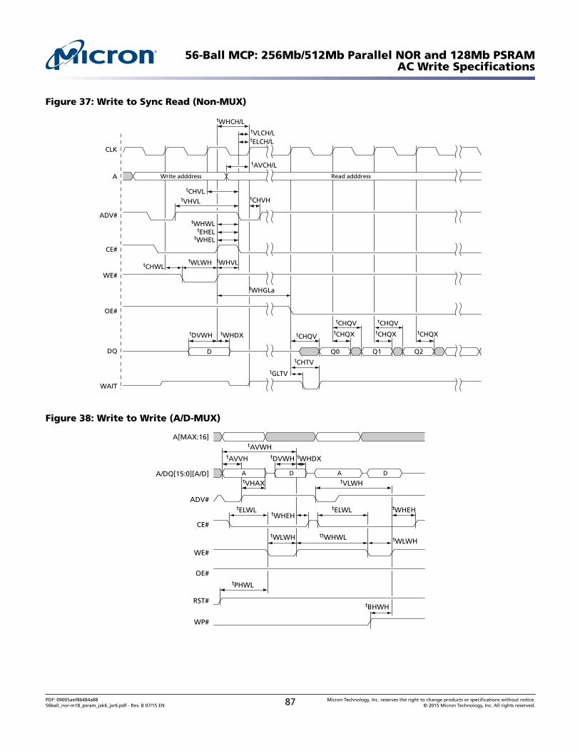
Figure 37: Write to Sync Read (Non-MUX)
A
CLK
ADV#
CE#
WE#
OE#
WAIT
DQ
tVLCH/LtELCH/L
tWHCH/L
tAVCH/L
tCHVHtVHVL
tCHVL
tGLTV
tCHQV
tWLWH tWHVLtCHWL
tCHTV
tWHGLa
tEHELtWHEL
tWHWL
tCHQVtCHQX
Q0
tCHQVtCHQX
Q1
tCHQX
Q2D
Write adddress Read adddress
tDVWH tWHDX
Figure 38: Write to Write (A/D-MUX)
A[MAX:16]tAVWH
tAVVH tDVWH tWHDX
tVHAX tVLWH
tWHEHtELWLtELWL
tPHWL
tBHWH
tWHEH
tWLWH ttWHWL tWLWH
A/DQ[15:0][A/D] A D A D
ADV#
CE#
WE#
OE#
RST#
WP#
56-Ball MCP: 256Mb/512Mb Parallel NOR and 128Mb PSRAMAC Write Specifications
PDF: 09005aef86484a8856ball_nor-m18_psram_jxk6_jxr6.pdf - Rev. B 07/15 EN 87 Micron Technology, Inc. reserves the right to change products or specifications without notice.
© 2015 Micron Technology, Inc. All rights reserved.
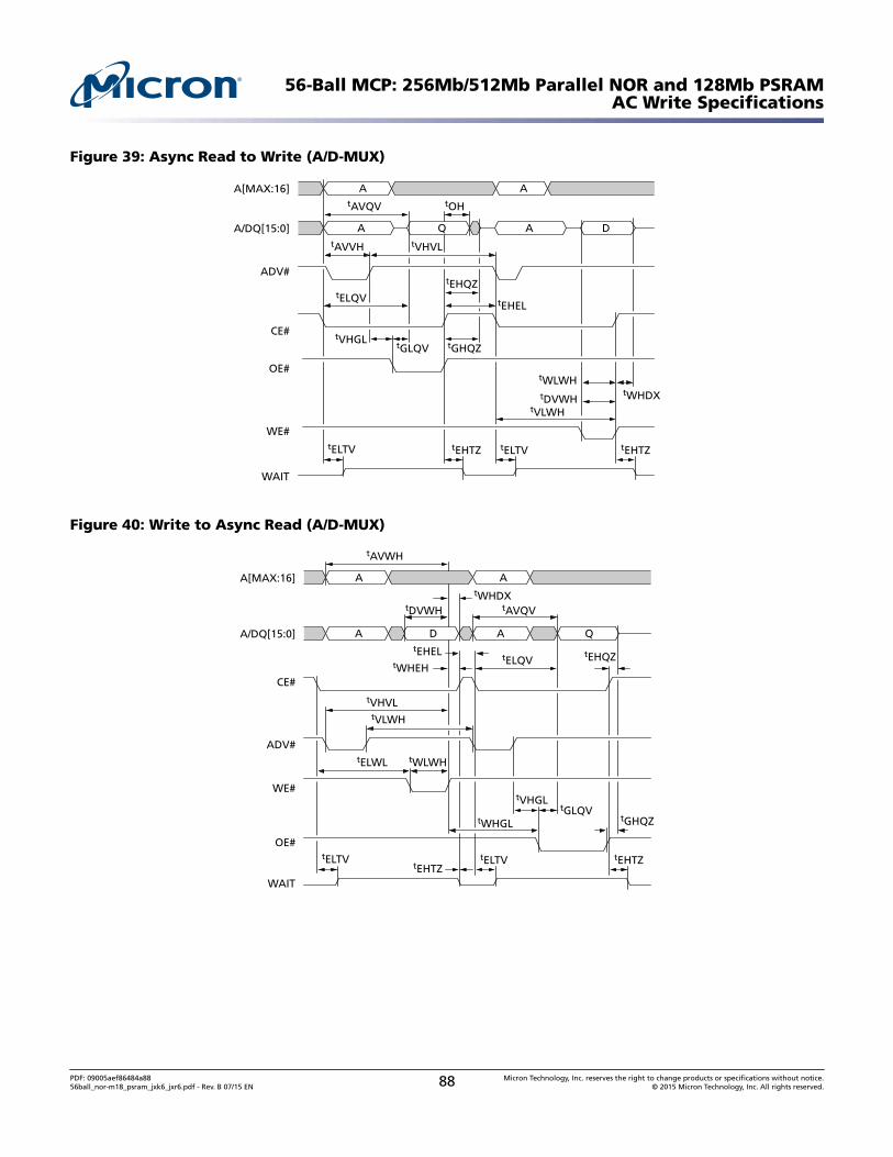
Figure 39: Async Read to Write (A/D-MUX)
tVHVL
A DA/DQ[15:0]
ADV#
CE#
OE#
WE#
WAIT
tAVVH
tAVQV tOH
tELTV tEHTZ tELTV tEHTZ
tEHEL
tEHQZ
tGHQZtGLQVtVHGL
tELQV
tWHDX
tWLWH
tVLWH
tDVWH
A
A[MAX:16] A A
Q
Figure 40: Write to Async Read (A/D-MUX)
tELQV
A QA/DQ[15:0]
CE#
ADV#
WE#
OE#
WAIT
tAVWH
tWHDX
tEHELtWHEH
tEHQZ
tDVWH tAVQV
tELTVtEHTZ
tELTV tEHTZ
tVLWH
tWLWHtELWL
tVHVL
tGHQZtGLQV
tWHGL
tVHGL
A
A[MAX:16] A A
D
56-Ball MCP: 256Mb/512Mb Parallel NOR and 128Mb PSRAMAC Write Specifications
PDF: 09005aef86484a8856ball_nor-m18_psram_jxk6_jxr6.pdf - Rev. B 07/15 EN 88 Micron Technology, Inc. reserves the right to change products or specifications without notice.
© 2015 Micron Technology, Inc. All rights reserved.
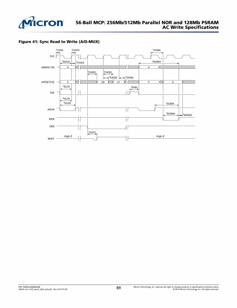
Figure 41: Sync Read to Write (A/D-MUX)
A[MAX:16]
CLK
CE#
ADV#
OE#
WAIT
tELCH
tAVCH tAVWHtCHAX
tCHQV
tVLVH
tVLCH
tCHQV
tCHQX tCHQX
tWHDX
tVLWH
WE#
tDVWH
tEHEL
tCHTV
High-ZHigh-Z
tCHVH tCHWLtCHVL
A/DQ[15:0] Q0 Q1 D
A
A
A
A
56-Ball MCP: 256Mb/512Mb Parallel NOR and 128Mb PSRAMAC Write Specifications
PDF: 09005aef86484a8856ball_nor-m18_psram_jxk6_jxr6.pdf - Rev. B 07/15 EN 89 Micron Technology, Inc. reserves the right to change products or specifications without notice.
© 2015 Micron Technology, Inc. All rights reserved.
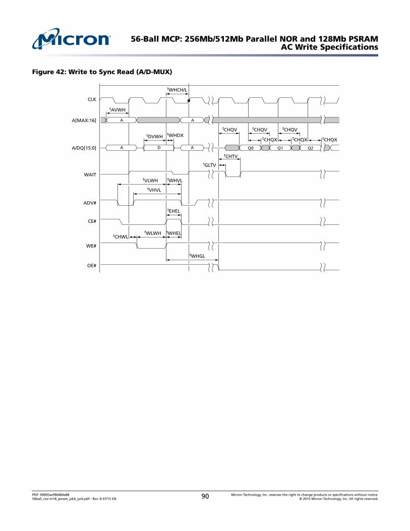
Figure 42: Write to Sync Read (A/D-MUX)
A[MAX:16]
CLK
CE#
ADV#
OE#
WAIT
tAVWH
tWHCH/L
tCHQV
tVLWH
tVHVL
tCHQV tCHQV
tCHQX tCHQX
WE#
tEHEL
tWHEL
tWHGL
tCHWLtWLWH
tWHVL
tCHTV
tGLTV
A/DQ[15:0] Q0 Q1 Q2
AA
A D A
tCHQXtDVWH
tWHDX
56-Ball MCP: 256Mb/512Mb Parallel NOR and 128Mb PSRAMAC Write Specifications
PDF: 09005aef86484a8856ball_nor-m18_psram_jxk6_jxr6.pdf - Rev. B 07/15 EN 90 Micron Technology, Inc. reserves the right to change products or specifications without notice.
© 2015 Micron Technology, Inc. All rights reserved.
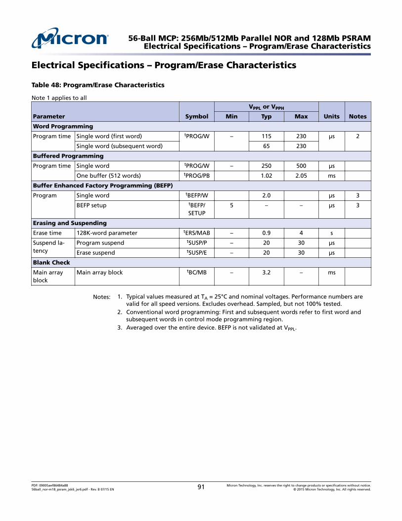
Electrical Specifications – Program/Erase Characteristics
Table 48: Program/Erase Characteristics
Note 1 applies to all
Parameter Symbol
VPPL or VPPH
Units NotesMin Typ Max
Word Programming
Program time Single word (first word) tPROG/W – 115 230 µs 2
Single word (subsequent word) 65 230
Buffered Programming
Program time Single word tPROG/W – 250 500 µs
One buffer (512 words) tPROG/PB 1.02 2.05 ms
Buffer Enhanced Factory Programming (BEFP)
Program Single word tBEFP/W 2.0 µs 3
BEFP setup tBEFP/SETUP
5 – – µs 3
Erasing and Suspending
Erase time 128K-word parameter tERS/MAB – 0.9 4 s
Suspend la-tency
Program suspend tSUSP/P – 20 30 µs
Erase suspend tSUSP/E – 20 30 µs
Blank Check
Main arrayblock
Main array block tBC/MB – 3.2 – ms
Notes: 1. Typical values measured at TA = 25°C and nominal voltages. Performance numbers arevalid for all speed versions. Excludes overhead. Sampled, but not 100% tested.
2. Conventional word programming: First and subsequent words refer to first word andsubsequent words in control mode programming region.
3. Averaged over the entire device. BEFP is not validated at VPPL.
56-Ball MCP: 256Mb/512Mb Parallel NOR and 128Mb PSRAMElectrical Specifications – Program/Erase Characteristics
PDF: 09005aef86484a8856ball_nor-m18_psram_jxk6_jxr6.pdf - Rev. B 07/15 EN 91 Micron Technology, Inc. reserves the right to change products or specifications without notice.
© 2015 Micron Technology, Inc. All rights reserved.
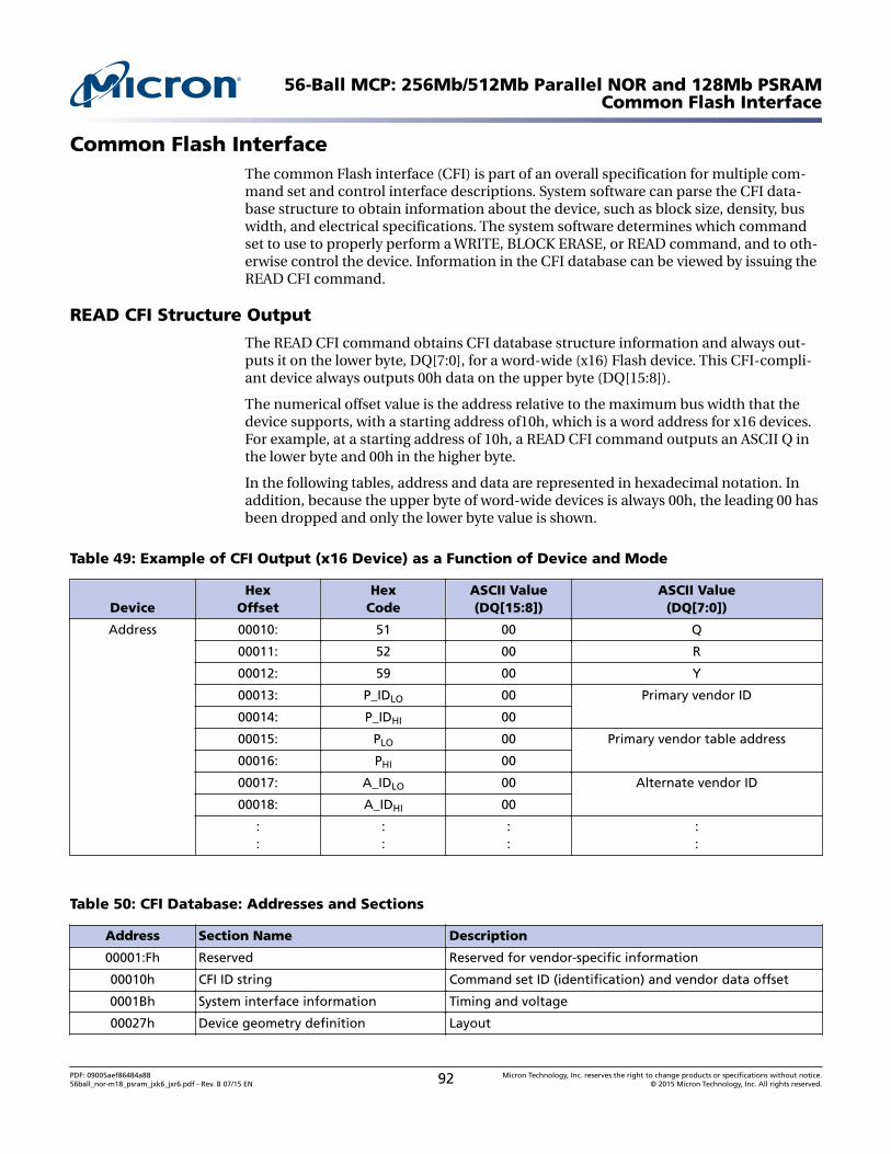
Common Flash InterfaceThe common Flash interface (CFI) is part of an overall specification for multiple com-mand set and control interface descriptions. System software can parse the CFI data-base structure to obtain information about the device, such as block size, density, buswidth, and electrical specifications. The system software determines which commandset to use to properly perform a WRITE, BLOCK ERASE, or READ command, and to oth-erwise control the device. Information in the CFI database can be viewed by issuing theREAD CFI command.
READ CFI Structure Output
The READ CFI command obtains CFI database structure information and always out-puts it on the lower byte, DQ[7:0], for a word-wide (x16) Flash device. This CFI-compli-ant device always outputs 00h data on the upper byte (DQ[15:8]).
The numerical offset value is the address relative to the maximum bus width that thedevice supports, with a starting address of10h, which is a word address for x16 devices.For example, at a starting address of 10h, a READ CFI command outputs an ASCII Q inthe lower byte and 00h in the higher byte.
In the following tables, address and data are represented in hexadecimal notation. Inaddition, because the upper byte of word-wide devices is always 00h, the leading 00 hasbeen dropped and only the lower byte value is shown.
Table 49: Example of CFI Output (x16 Device) as a Function of Device and Mode
DeviceHex
OffsetHex
CodeASCII Value(DQ[15:8])
ASCII Value(DQ[7:0])
Address 00010: 51 00 Q
00011: 52 00 R
00012: 59 00 Y
00013: P_IDLO 00 Primary vendor ID
00014: P_IDHI 00
00015: PLO 00 Primary vendor table address
00016: PHI 00
00017: A_IDLO 00 Alternate vendor ID
00018: A_IDHI 00
::
::
::
::
Table 50: CFI Database: Addresses and Sections
Address Section Name Description
00001:Fh Reserved Reserved for vendor-specific information
00010h CFI ID string Command set ID (identification) and vendor data offset
0001Bh System interface information Timing and voltage
00027h Device geometry definition Layout
56-Ball MCP: 256Mb/512Mb Parallel NOR and 128Mb PSRAMCommon Flash Interface
PDF: 09005aef86484a8856ball_nor-m18_psram_jxk6_jxr6.pdf - Rev. B 07/15 EN 92 Micron Technology, Inc. reserves the right to change products or specifications without notice.
© 2015 Micron Technology, Inc. All rights reserved.
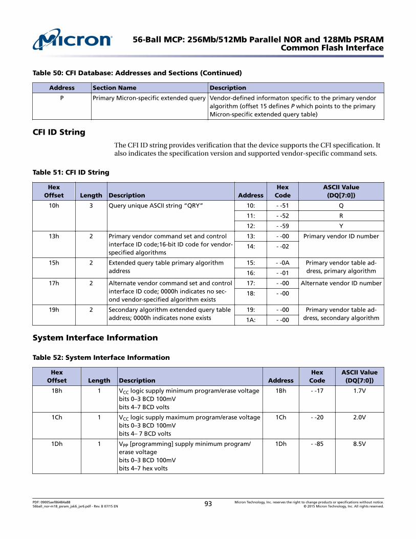
Table 50: CFI Database: Addresses and Sections (Continued)
Address Section Name Description
P Primary Micron-specific extended query Vendor-defined informaton specific to the primary vendoralgorithm (offset 15 defines P which points to the primaryMicron-specific extended query table)
CFI ID String
The CFI ID string provides verification that the device supports the CFI specification. Italso indicates the specification version and supported vendor-specific command sets.
Table 51: CFI ID String
HexOffset Length Description Address
HexCode
ASCII Value(DQ[7:0])
10h 3 Query unique ASCII string “QRY” 10: - -51 Q
11: - -52 R
12: - -59 Y
13h 2 Primary vendor command set and controlinterface ID code;16-bit ID code for vendor-specified algorithms
13: - -00 Primary vendor ID number
14: - -02
15h 2 Extended query table primary algorithmaddress
15: - -0A Primary vendor table ad-dress, primary algorithm16: - -01
17h 2 Alternate vendor command set and controlinterface ID code; 0000h indicates no sec-ond vendor-specified algorithm exists
17: - -00 Alternate vendor ID number
18: - -00
19h 2 Secondary algorithm extended query tableaddress; 0000h indicates none exists
19: - -00 Primary vendor table ad-dress, secondary algorithm1A: - -00
System Interface Information
Table 52: System Interface Information
HexOffset Length Description Address
HexCode
ASCII Value(DQ[7:0])
1Bh 1 VCC logic supply minimum program/erase voltagebits 0–3 BCD 100mVbits 4–7 BCD volts
1Bh - -17 1.7V
1Ch 1 VCC logic supply maximum program/erase voltagebits 0–3 BCD 100mVbits 4– 7 BCD volts
1Ch - -20 2.0V
1Dh 1 VPP [programming] supply minimum program/erase voltagebits 0–3 BCD 100mVbits 4–7 hex volts
1Dh - -85 8.5V
56-Ball MCP: 256Mb/512Mb Parallel NOR and 128Mb PSRAMCommon Flash Interface
PDF: 09005aef86484a8856ball_nor-m18_psram_jxk6_jxr6.pdf - Rev. B 07/15 EN 93 Micron Technology, Inc. reserves the right to change products or specifications without notice.
© 2015 Micron Technology, Inc. All rights reserved.
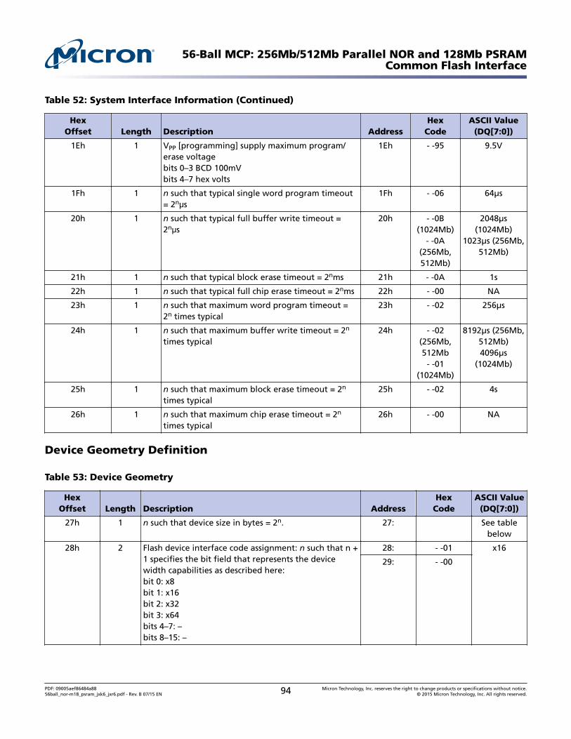
Table 52: System Interface Information (Continued)
HexOffset Length Description Address
HexCode
ASCII Value(DQ[7:0])
1Eh 1 VPP [programming] supply maximum program/erase voltagebits 0–3 BCD 100mVbits 4–7 hex volts
1Eh - -95 9.5V
1Fh 1 n such that typical single word program timeout= 2nμs
1Fh - -06 64µs
20h 1 n such that typical full buffer write timeout =2nμs
20h - -0B(1024Mb)
- -0A(256Mb,512Mb)
2048µs(1024Mb)
1023µs (256Mb,512Mb)
21h 1 n such that typical block erase timeout = 2nms 21h - -0A 1s
22h 1 n such that typical full chip erase timeout = 2nms 22h - -00 NA
23h 1 n such that maximum word program timeout =2n times typical
23h - -02 256µs
24h 1 n such that maximum buffer write timeout = 2n
times typical24h - -02
(256Mb,512Mb
- -01(1024Mb)
8192µs (256Mb,512Mb)4096µs
(1024Mb)
25h 1 n such that maximum block erase timeout = 2n
times typical25h - -02 4s
26h 1 n such that maximum chip erase timeout = 2n
times typical26h - -00 NA
Device Geometry Definition
Table 53: Device Geometry
HexOffset Length Description Address
HexCode
ASCII Value(DQ[7:0])
27h 1 n such that device size in bytes = 2n. 27: See tablebelow
28h 2 Flash device interface code assignment: n such that n +1 specifies the bit field that represents the devicewidth capabilities as described here:bit 0: x8bit 1: x16bit 2: x32bit 3: x64bits 4–7: –bits 8–15: –
28: - -01 x16
29: - -00
56-Ball MCP: 256Mb/512Mb Parallel NOR and 128Mb PSRAMCommon Flash Interface
PDF: 09005aef86484a8856ball_nor-m18_psram_jxk6_jxr6.pdf - Rev. B 07/15 EN 94 Micron Technology, Inc. reserves the right to change products or specifications without notice.
© 2015 Micron Technology, Inc. All rights reserved.
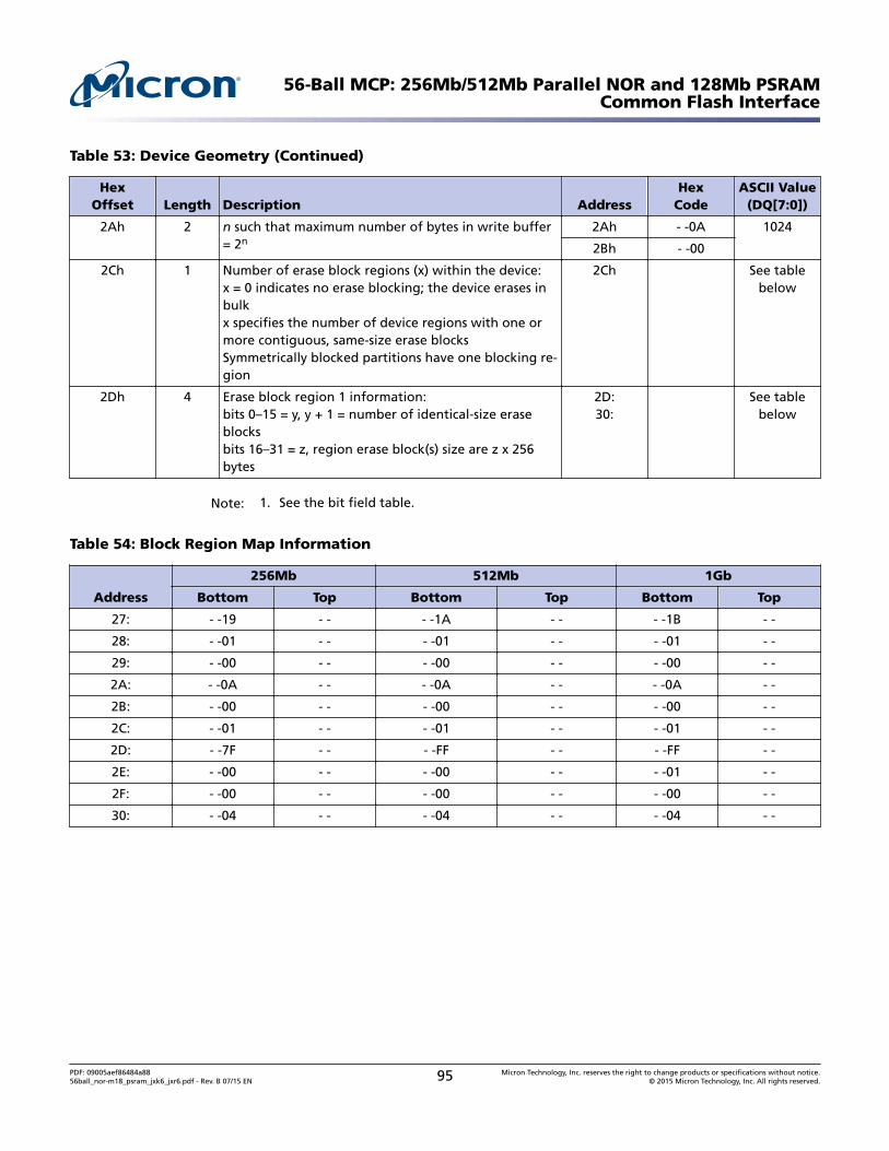
Table 53: Device Geometry (Continued)
HexOffset Length Description Address
HexCode
ASCII Value(DQ[7:0])
2Ah 2 n such that maximum number of bytes in write buffer= 2n
2Ah - -0A 1024
2Bh - -00
2Ch 1 Number of erase block regions (x) within the device:x = 0 indicates no erase blocking; the device erases inbulkx specifies the number of device regions with one ormore contiguous, same-size erase blocksSymmetrically blocked partitions have one blocking re-gion
2Ch See tablebelow
2Dh 4 Erase block region 1 information:bits 0–15 = y, y + 1 = number of identical-size eraseblocksbits 16–31 = z, region erase block(s) size are z x 256bytes
2D:30:
See tablebelow
Note: 1. See the bit field table.
Table 54: Block Region Map Information
Address
256Mb 512Mb 1Gb
Bottom Top Bottom Top Bottom Top
27: - -19 - - - -1A - - - -1B - -
28: - -01 - - - -01 - - - -01 - -
29: - -00 - - - -00 - - - -00 - -
2A: - -0A - - - -0A - - - -0A - -
2B: - -00 - - - -00 - - - -00 - -
2C: - -01 - - - -01 - - - -01 - -
2D: - -7F - - - -FF - - - -FF - -
2E: - -00 - - - -00 - - - -01 - -
2F: - -00 - - - -00 - - - -00 - -
30: - -04 - - - -04 - - - -04 - -
56-Ball MCP: 256Mb/512Mb Parallel NOR and 128Mb PSRAMCommon Flash Interface
PDF: 09005aef86484a8856ball_nor-m18_psram_jxk6_jxr6.pdf - Rev. B 07/15 EN 95 Micron Technology, Inc. reserves the right to change products or specifications without notice.
© 2015 Micron Technology, Inc. All rights reserved.
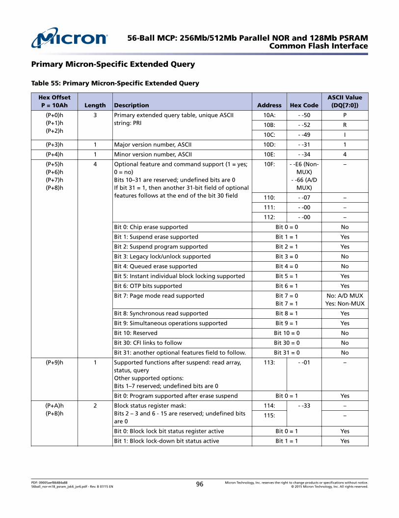
Primary Micron-Specific Extended Query
Table 55: Primary Micron-Specific Extended Query
Hex OffsetP = 10Ah Length Description Address Hex Code
ASCII Value(DQ[7:0])
(P+0)h(P+1)h(P+2)h
3 Primary extended query table, unique ASCIIstring: PRI
10A: - -50 P
10B: - -52 R
10C: - -49 I
(P+3)h 1 Major version number, ASCII 10D: - -31 1
(P+4)h 1 Minor version number, ASCII 10E: - -34 4
(P+5)h(P+6)h(P+7)h(P+8)h
4 Optional feature and command support (1 = yes;0 = no)Bits 10–31 are reserved; undefined bits are 0If bit 31 = 1, then another 31-bit field of optionalfeatures follows at the end of the bit 30 field
10F: - -E6 (Non-MUX)
- -66 (A/DMUX)
–
110: - -07 –
111: - -00 –
112: - -00 –
Bit 0: Chip erase supported Bit 0 = 0 No
Bit 1: Suspend erase supported Bit 1 = 1 Yes
Bit 2: Suspend program supported Bit 2 = 1 Yes
Bit 3: Legacy lock/unlock supported Bit 3 = 0 No
Bit 4: Queued erase supported Bit 4 = 0 No
Bit 5: Instant individual block locking supported Bit 5 = 1 Yes
Bit 6: OTP bits supported Bit 6 = 1 Yes
Bit 7: Page mode read supported Bit 7 = 0Bit 7 = 1
No: A/D MUXYes: Non-MUX
Bit 8: Synchronous read supported Bit 8 = 1 Yes
Bit 9: Simultaneous operations supported Bit 9 = 1 Yes
Bit 10: Reserved Bit 10 = 0 No
Bit 30: CFI links to follow Bit 30 = 0 No
Bit 31: another optional features field to follow. Bit 31 = 0 No
(P+9)h 1 Supported functions after suspend: read array,status, queryOther supported options:Bits 1–7 reserved; undefined bits are 0
113: - -01 –
Bit 0: Program supported after erase suspend Bit 0 = 1 Yes
(P+A)h(P+B)h
2 Block status register mask:Bits 2 – 3 and 6 - 15 are reserved; undefined bitsare 0
114: - -33 –
115: –
Bit 0: Block lock bit status register active Bit 0 = 1 Yes
Bit 1: Block lock-down bit status active Bit 1 = 1 Yes
56-Ball MCP: 256Mb/512Mb Parallel NOR and 128Mb PSRAMCommon Flash Interface
PDF: 09005aef86484a8856ball_nor-m18_psram_jxk6_jxr6.pdf - Rev. B 07/15 EN 96 Micron Technology, Inc. reserves the right to change products or specifications without notice.
© 2015 Micron Technology, Inc. All rights reserved.
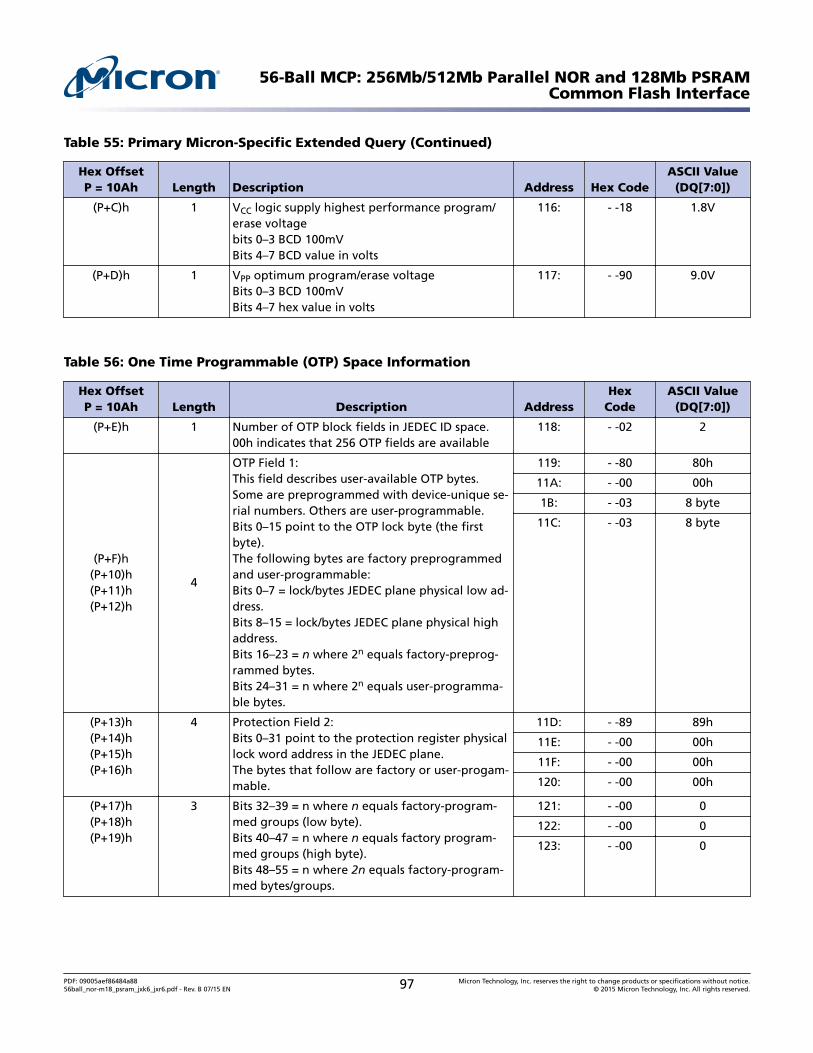
Table 55: Primary Micron-Specific Extended Query (Continued)
Hex OffsetP = 10Ah Length Description Address Hex Code
ASCII Value(DQ[7:0])
(P+C)h 1 VCC logic supply highest performance program/erase voltagebits 0–3 BCD 100mVBits 4–7 BCD value in volts
116: - -18 1.8V
(P+D)h 1 VPP optimum program/erase voltageBits 0–3 BCD 100mVBits 4–7 hex value in volts
117: - -90 9.0V
Table 56: One Time Programmable (OTP) Space Information
Hex OffsetP = 10Ah Length Description Address
HexCode
ASCII Value(DQ[7:0])
(P+E)h 1 Number of OTP block fields in JEDEC ID space.00h indicates that 256 OTP fields are available
118: - -02 2
(P+F)h(P+10)h(P+11)h(P+12)h
4
OTP Field 1:This field describes user-available OTP bytes.Some are preprogrammed with device-unique se-rial numbers. Others are user-programmable.Bits 0–15 point to the OTP lock byte (the firstbyte).The following bytes are factory preprogrammedand user-programmable:Bits 0–7 = lock/bytes JEDEC plane physical low ad-dress.Bits 8–15 = lock/bytes JEDEC plane physical highaddress.Bits 16–23 = n where 2n equals factory-preprog-rammed bytes.Bits 24–31 = n where 2n equals user-programma-ble bytes.
119: - -80 80h
11A: - -00 00h
1B: - -03 8 byte
11C: - -03 8 byte
(P+13)h(P+14)h(P+15)h(P+16)h
4 Protection Field 2:Bits 0–31 point to the protection register physicallock word address in the JEDEC plane.The bytes that follow are factory or user-progam-mable.
11D: - -89 89h
11E: - -00 00h
11F: - -00 00h
120: - -00 00h
(P+17)h(P+18)h(P+19)h
3 Bits 32–39 = n where n equals factory-program-med groups (low byte).Bits 40–47 = n where n equals factory program-med groups (high byte).Bits 48–55 = n where 2n equals factory-program-med bytes/groups.
121: - -00 0
122: - -00 0
123: - -00 0
56-Ball MCP: 256Mb/512Mb Parallel NOR and 128Mb PSRAMCommon Flash Interface
PDF: 09005aef86484a8856ball_nor-m18_psram_jxk6_jxr6.pdf - Rev. B 07/15 EN 97 Micron Technology, Inc. reserves the right to change products or specifications without notice.
© 2015 Micron Technology, Inc. All rights reserved.
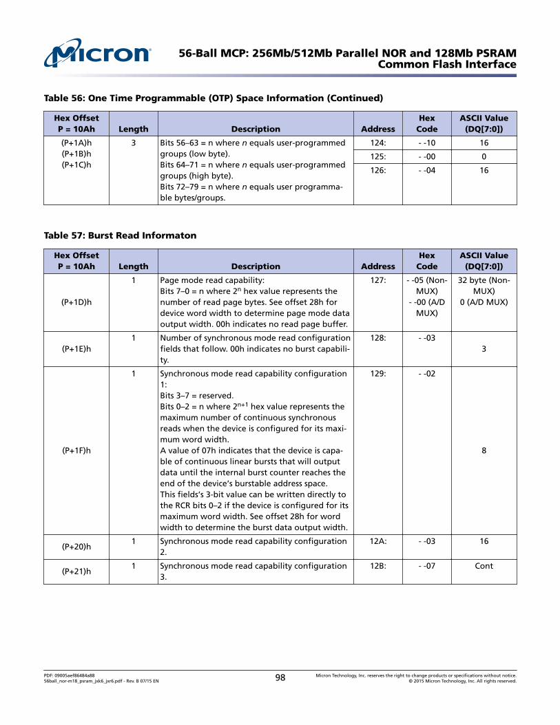
Table 56: One Time Programmable (OTP) Space Information (Continued)
Hex OffsetP = 10Ah Length Description Address
HexCode
ASCII Value(DQ[7:0])
(P+1A)h(P+1B)h(P+1C)h
3 Bits 56–63 = n where n equals user-programmedgroups (low byte).Bits 64–71 = n where n equals user-programmedgroups (high byte).Bits 72–79 = n where n equals user programma-ble bytes/groups.
124: - -10 16
125: - -00 0
126: - -04 16
Table 57: Burst Read Informaton
Hex OffsetP = 10Ah Length Description Address
HexCode
ASCII Value(DQ[7:0])
(P+1D)h
1 Page mode read capability:Bits 7–0 = n where 2n hex value represents thenumber of read page bytes. See offset 28h fordevice word width to determine page mode dataoutput width. 00h indicates no read page buffer.
127: - -05 (Non-MUX)
- -00 (A/DMUX)
32 byte (Non-MUX)
0 (A/D MUX)
(P+1E)h1 Number of synchronous mode read configuration
fields that follow. 00h indicates no burst capabili-ty.
128: - -033
(P+1F)h
1 Synchronous mode read capability configuration1:Bits 3–7 = reserved.Bits 0–2 = n where 2n+1 hex value represents themaximum number of continuous synchronousreads when the device is configured for its maxi-mum word width.A value of 07h indicates that the device is capa-ble of continuous linear bursts that will outputdata until the internal burst counter reaches theend of the device’s burstable address space.This fields’s 3-bit value can be written directly tothe RCR bits 0–2 if the device is configured for itsmaximum word width. See offset 28h for wordwidth to determine the burst data output width.
129: - -02
8
(P+20)h1 Synchronous mode read capability configuration
2.12A: - -03 16
(P+21)h1 Synchronous mode read capability configuration
3.12B: - -07 Cont
56-Ball MCP: 256Mb/512Mb Parallel NOR and 128Mb PSRAMCommon Flash Interface
PDF: 09005aef86484a8856ball_nor-m18_psram_jxk6_jxr6.pdf - Rev. B 07/15 EN 98 Micron Technology, Inc. reserves the right to change products or specifications without notice.
© 2015 Micron Technology, Inc. All rights reserved.
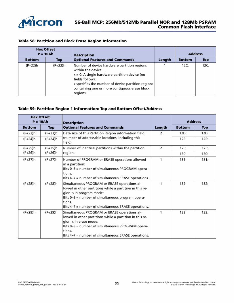
Table 58: Partition and Block Erase Region Information
Hex OffsetP = 10Ah Description
Optional Features and Commands Length
Address
Bottom Top Bottom Top
(P+22)h (P+22)h Number of device hardware partition regionswithin the device:x = 0: A single hardware partition device (nofields follow).x specifies the number of device partition regionscontaining one or more contiguous erase blockregions
1 12C: 12C:
Table 59: Partition Region 1 Information: Top and Bottom Offset/Address
Hex OffsetP = 10Ah Description
Optional Features and Commands Length
Address
Bottom Top Bottom Top
(P+23)h (P+23)h Data size of this Partition Region information field:(number of addressable locations, including thisfield).
2 12D: 12D:
(P+24)h (P+24)h 12E: 12E:
(P+25)h(P+26)h
(P+25)h(P+26)h
Number of identical partitions within the partitionregion.
2 12F: 12F:
130: 130:
(P+27)h (P+27)h Number of PROGRAM or ERASE operations allowedin a partition:Bits 0–3 = number of simultaneous PROGRAM opera-tions.Bits 4–7 = number of simultaneous ERASE operations.
1 131: 131:
(P+28)h (P+28)h Simultaneous PROGRAM or ERASE operations al-lowed in other partitions while a partition in this re-gion is in program mode:Bits 0–3 = number of simultaneous program opera-tions.Bits 4–7 = number of simultaneous ERASE operations.
1 132: 132:
(P+29)h (P+29)h Simultaneous PROGRAM or ERASE operations al-lowed in other partitions while a partition in this re-gion is in erase mode:Bits 0–3 = number of simultaneous PROGRAM opera-tions.Bits 4–7 = number of simultaneous ERASE operations.
1 133: 133:
56-Ball MCP: 256Mb/512Mb Parallel NOR and 128Mb PSRAMCommon Flash Interface
PDF: 09005aef86484a8856ball_nor-m18_psram_jxk6_jxr6.pdf - Rev. B 07/15 EN 99 Micron Technology, Inc. reserves the right to change products or specifications without notice.
© 2015 Micron Technology, Inc. All rights reserved.
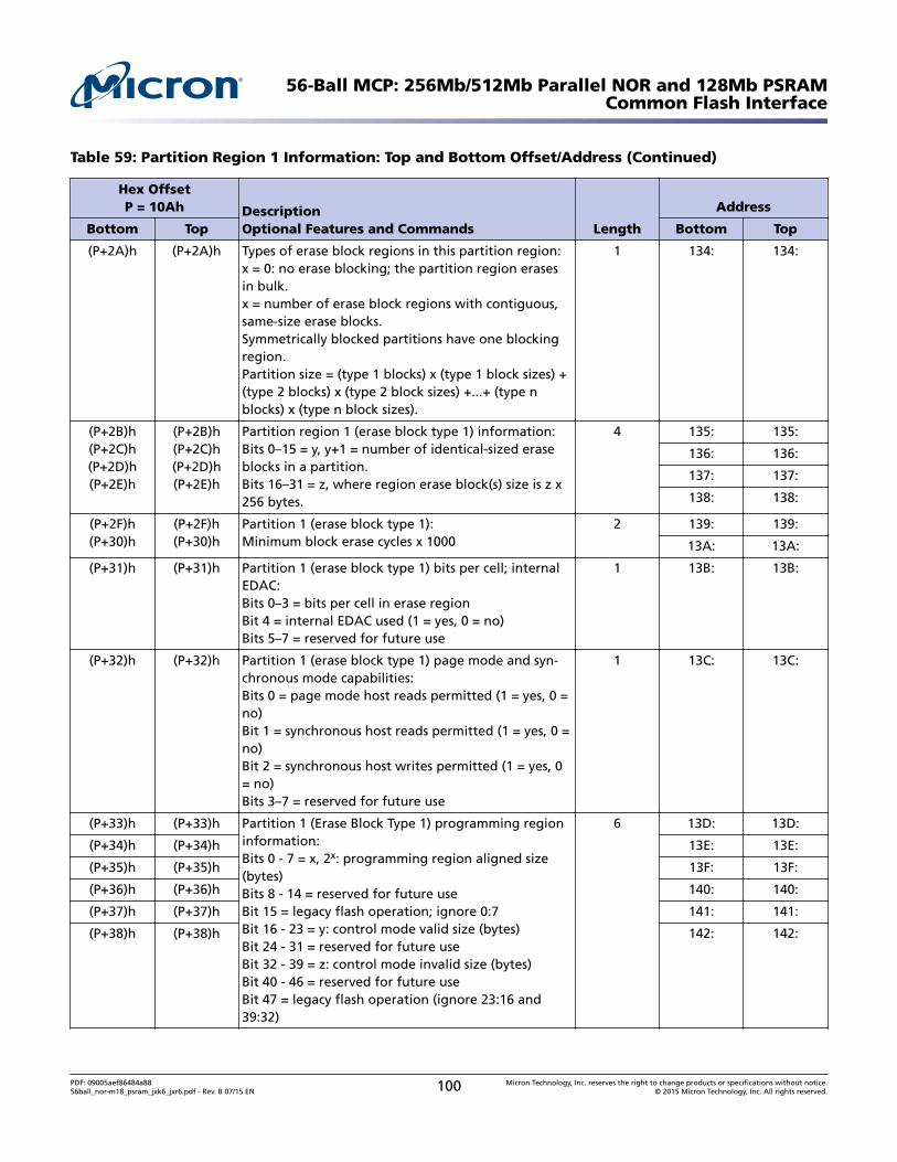
Table 59: Partition Region 1 Information: Top and Bottom Offset/Address (Continued)
Hex OffsetP = 10Ah Description
Optional Features and Commands Length
Address
Bottom Top Bottom Top
(P+2A)h (P+2A)h Types of erase block regions in this partition region:x = 0: no erase blocking; the partition region erasesin bulk.x = number of erase block regions with contiguous,same-size erase blocks.Symmetrically blocked partitions have one blockingregion.Partition size = (type 1 blocks) x (type 1 block sizes) +(type 2 blocks) x (type 2 block sizes) +...+ (type nblocks) x (type n block sizes).
1 134: 134:
(P+2B)h(P+2C)h(P+2D)h(P+2E)h
(P+2B)h(P+2C)h(P+2D)h(P+2E)h
Partition region 1 (erase block type 1) information:Bits 0–15 = y, y+1 = number of identical-sized eraseblocks in a partition.Bits 16–31 = z, where region erase block(s) size is z x256 bytes.
4 135: 135:
136: 136:
137: 137:
138: 138:
(P+2F)h(P+30)h
(P+2F)h(P+30)h
Partition 1 (erase block type 1):Minimum block erase cycles x 1000
2 139: 139:
13A: 13A:
(P+31)h (P+31)h Partition 1 (erase block type 1) bits per cell; internalEDAC:Bits 0–3 = bits per cell in erase regionBit 4 = internal EDAC used (1 = yes, 0 = no)Bits 5–7 = reserved for future use
1 13B: 13B:
(P+32)h (P+32)h Partition 1 (erase block type 1) page mode and syn-chronous mode capabilities:Bits 0 = page mode host reads permitted (1 = yes, 0 =no)Bit 1 = synchronous host reads permitted (1 = yes, 0 =no)Bit 2 = synchronous host writes permitted (1 = yes, 0= no)Bits 3–7 = reserved for future use
1 13C: 13C:
(P+33)h (P+33)h Partition 1 (Erase Block Type 1) programming regioninformation:Bits 0 - 7 = x, 2x: programming region aligned size(bytes)Bits 8 - 14 = reserved for future useBit 15 = legacy flash operation; ignore 0:7Bit 16 - 23 = y: control mode valid size (bytes)Bit 24 - 31 = reserved for future useBit 32 - 39 = z: control mode invalid size (bytes)Bit 40 - 46 = reserved for future useBit 47 = legacy flash operation (ignore 23:16 and39:32)
6 13D: 13D:
(P+34)h (P+34)h 13E: 13E:
(P+35)h (P+35)h 13F: 13F:
(P+36)h (P+36)h 140: 140:
(P+37)h (P+37)h 141: 141:
(P+38)h (P+38)h 142: 142:
56-Ball MCP: 256Mb/512Mb Parallel NOR and 128Mb PSRAMCommon Flash Interface
PDF: 09005aef86484a8856ball_nor-m18_psram_jxk6_jxr6.pdf - Rev. B 07/15 EN 100 Micron Technology, Inc. reserves the right to change products or specifications without notice.
© 2015 Micron Technology, Inc. All rights reserved.
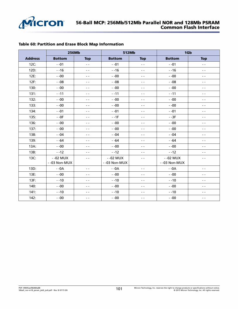
Table 60: Partition and Erase Block Map Information
Address
256Mb 512Mb 1Gb
Bottom Top Bottom Top Bottom Top
12C: - -01 - - - -01 - - - -01 - -
12D: - -16 - - - -16 - - - -16 - -
12E: - -00 - - - -00 - - - -00 - -
12F: - -08 - - - -08 - - - -08 - -
130: - -00 - - - -00 - - - -00 - -
131: - -11 - - - -11 - - - -11 - -
132: - -00 - - - -00 - - - -00 - -
133: - -00 - - - -00 - - - -00 - -
134: - -01 - - - -01 - - - -01 - -
135: - -0F - - - -1F - - - -3F - -
136: - -00 - - - -00 - - - -00 - -
137: - -00 - - - -00 - - - -00 - -
138: - -04 - - - -04 - - - -04 - -
139: - -64 - - - -64 - - - -64 - -
13A: - -00 - - - -00 - - - -00 - -
13B: - -12 - - - -12 - - - -12 - -
13C: - -02 MUX- -03 Non-MUX
- - - -02 MUX- -03 Non-MUX
- - - -02 MUX- -03 Non-MUX
- -
13D: - -0A - - - -0A - - - -0A - -
13E: - -00 - - - -00 - - - -00 - -
13F: - -10 - - - -10 - - - -10 - -
140: - -00 - - - -00 - - - -00 - -
141: - -10 - - - -10 - - - -10 - -
142: - -00 - - - -00 - - - -00 - -
56-Ball MCP: 256Mb/512Mb Parallel NOR and 128Mb PSRAMCommon Flash Interface
PDF: 09005aef86484a8856ball_nor-m18_psram_jxk6_jxr6.pdf - Rev. B 07/15 EN 101 Micron Technology, Inc. reserves the right to change products or specifications without notice.
© 2015 Micron Technology, Inc. All rights reserved.
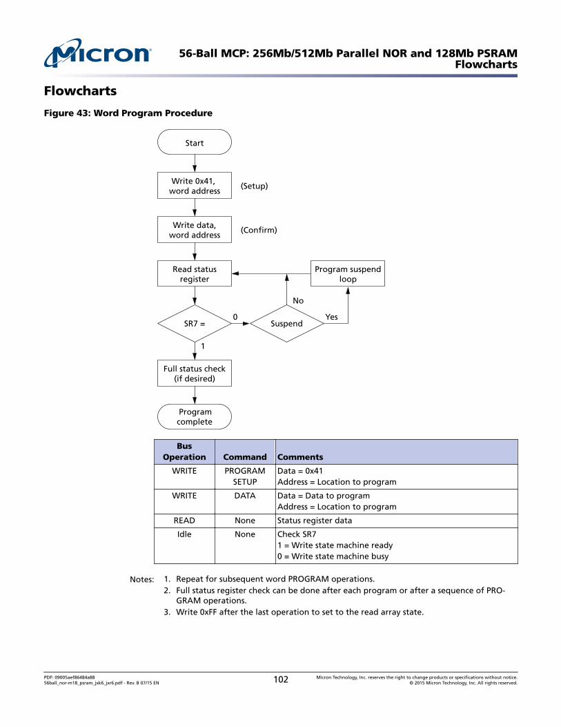
Flowcharts
Figure 43: Word Program Procedure
0
Programcomplete
1
SR7 =
Write 0x41, word address
Start
Write data,word address
(Setup)
(Confirm)
Read statusregister
Program suspendloop
Yes
No
Suspend
Full status check(if desired)
BusOperation Command Comments
WRITE PROGRAMSETUP
Data = 0x41Address = Location to program
WRITE DATA Data = Data to programAddress = Location to program
READ None Status register data
Idle None Check SR71 = Write state machine ready0 = Write state machine busy
Notes: 1. Repeat for subsequent word PROGRAM operations.2. Full status register check can be done after each program or after a sequence of PRO-
GRAM operations.3. Write 0xFF after the last operation to set to the read array state.
56-Ball MCP: 256Mb/512Mb Parallel NOR and 128Mb PSRAMFlowcharts
PDF: 09005aef86484a8856ball_nor-m18_psram_jxk6_jxr6.pdf - Rev. B 07/15 EN 102 Micron Technology, Inc. reserves the right to change products or specifications without notice.
© 2015 Micron Technology, Inc. All rights reserved.
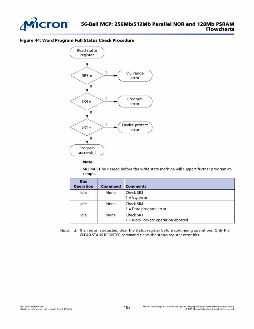
Figure 44: Word Program Full Status Check Procedure
Programsuccessful
1
0
1
0
1
0
Read statusregister
SR3 =
SR4 =
SR1 =
Programerror
Device protecterror
VPP rangeerror
Note:
SR3 MUST be cleared before the write state machine will support further program at-tempts.
BusOperation Command Comments
Idle None Check SR31 = VPP error
Idle None Check SR41 = Data program error
Idle None Check SR11 = Block locked; operation aborted
Note: 2. If an error is detected, clear the status register before continuing operations. Only theCLEAR STAUS REGISTER command clears the status register error bits.
56-Ball MCP: 256Mb/512Mb Parallel NOR and 128Mb PSRAMFlowcharts
PDF: 09005aef86484a8856ball_nor-m18_psram_jxk6_jxr6.pdf - Rev. B 07/15 EN 103 Micron Technology, Inc. reserves the right to change products or specifications without notice.
© 2015 Micron Technology, Inc. All rights reserved.
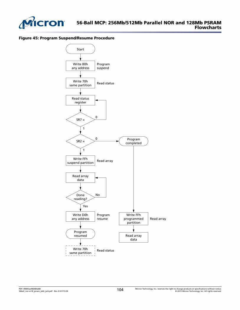
Figure 45: Program Suspend/Resume Procedure
0
1
SR7 =
Write B0hany address
Start
Write 70hsame partition
Programsuspend
Read status
Write FFhsuspend partition
Read array
Programresume
Read status
Write D0hany address
Write 70hsame partition
Read arraydata
Write FFhprogrammed
partitionRead array
Read arraydata
Read statusregister
0
1
SR2 =
Programresumed
No
Yes
Donereading?
Programcompleted
56-Ball MCP: 256Mb/512Mb Parallel NOR and 128Mb PSRAMFlowcharts
PDF: 09005aef86484a8856ball_nor-m18_psram_jxk6_jxr6.pdf - Rev. B 07/15 EN 104 Micron Technology, Inc. reserves the right to change products or specifications without notice.
© 2015 Micron Technology, Inc. All rights reserved.
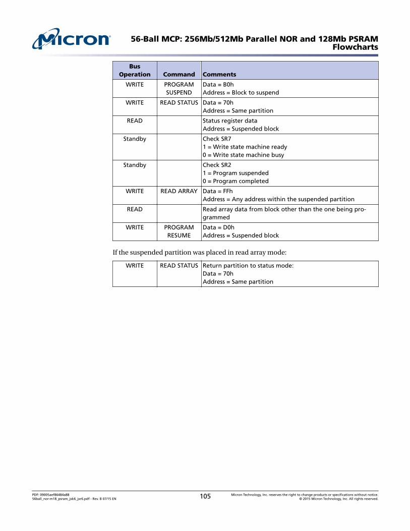
BusOperation Command Comments
WRITE PROGRAMSUSPEND
Data = B0hAddress = Block to suspend
WRITE READ STATUS Data = 70hAddress = Same partition
READ Status register dataAddress = Suspended block
Standby Check SR71 = Write state machine ready0 = Write state machine busy
Standby Check SR21 = Program suspended0 = Program completed
WRITE READ ARRAY Data = FFhAddress = Any address within the suspended partition
READ Read array data from block other than the one being pro-grammed
WRITE PROGRAMRESUME
Data = D0hAddress = Suspended block
If the suspended partition was placed in read array mode:
WRITE READ STATUS Return partition to status mode:Data = 70hAddress = Same partition
56-Ball MCP: 256Mb/512Mb Parallel NOR and 128Mb PSRAMFlowcharts
PDF: 09005aef86484a8856ball_nor-m18_psram_jxk6_jxr6.pdf - Rev. B 07/15 EN 105 Micron Technology, Inc. reserves the right to change products or specifications without notice.
© 2015 Micron Technology, Inc. All rights reserved.
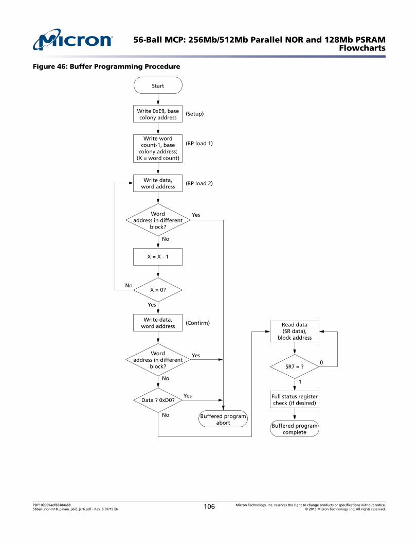
Figure 46: Buffer Programming Procedure
No
Yes
X = 0?
Wordaddress in different
block?
Wordaddress in different
block?
Write 0xE9, basecolony address
Start
Write wordcount-1, base
colony address;(X = word count)
(Setup)
(BP load 1)
Write data,word address
(BP load 2)
Write data,word address
(Confirm)
X = X - 1
Yes
No
Yes
Yes
No
No
Data ? 0xD0?
Buffered programabort
Read data(SR data),
block address
Full status registercheck (if desired)
Buffered programcomplete
0
1
SR7 = ?
56-Ball MCP: 256Mb/512Mb Parallel NOR and 128Mb PSRAMFlowcharts
PDF: 09005aef86484a8856ball_nor-m18_psram_jxk6_jxr6.pdf - Rev. B 07/15 EN 106 Micron Technology, Inc. reserves the right to change products or specifications without notice.
© 2015 Micron Technology, Inc. All rights reserved.
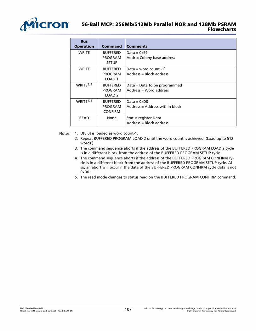
BusOperation Command Comments
WRITE BUFFEREDPROGRAM
SETUP
Data = 0xE9Addr = Colony base address
WRITE BUFFEREDPROGRAM
LOAD 1
Data = word count -11
Address = Block address
WRITE2, 3 BUFFEREDPROGRAM
LOAD 2
Data = Data to be programmedAddress = Word address
WRITE4, 5 BUFFEREDPROGRAMCONFIRM
Data = 0xD0Address = Address within block
READ None Status register DataAddress = Block address
Notes: 1. D[8:0] is loaded as word count-1.2. Repeat BUFFERED PROGRAM LOAD 2 until the word count is achieved. (Load up to 512
words.)3. The command sequence aborts if the address of the BUFFERED PROGRAM LOAD 2 cycle
is in a different block from the address of the BUFFERED PROGRAM SETUP cycle.4. The command sequence aborts if the address of the BUFFERED PROGRAM CONFIRM cy-
cle is in a different block from the address of the BUFFERED PROGRAM SETUP cycle. Al-so, an abort will occur if the data of the BUFFERED PROGRAM CONFIRM cycle data is not0xD0.
5. The read mode changes to status read on the BUFFERED PROGRAM CONFIRM command.
56-Ball MCP: 256Mb/512Mb Parallel NOR and 128Mb PSRAMFlowcharts
PDF: 09005aef86484a8856ball_nor-m18_psram_jxk6_jxr6.pdf - Rev. B 07/15 EN 107 Micron Technology, Inc. reserves the right to change products or specifications without notice.
© 2015 Micron Technology, Inc. All rights reserved.
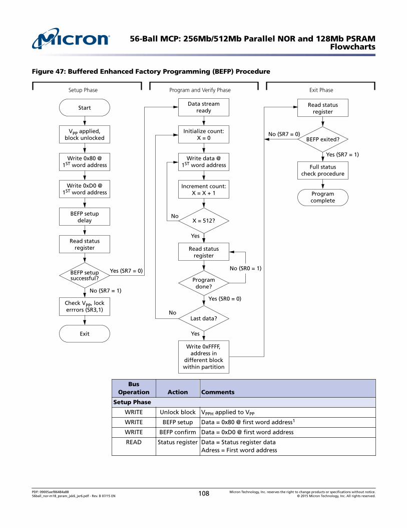
Figure 47: Buffered Enhanced Factory Programming (BEFP) Procedure
No (SR7 = 1)
Yes (SR7 = 0)
Yes (SR0 = 0)
BEFP setupsuccessful?
VPP applied,block unlocked
Start
Exit
Write 0x80 @1ST word address
Write 0xD0 @1ST word address
BEFP setupdelay
Read statusregister
Check VPP, lockerrrors (SR3,1)
Yes
NoX = 512?
Initialize count:X = 0
Data streamready
Write data @1ST word address
Increment count:X = X + 1
Read statusregister
Programdone?
Yes
NoLast data?
Write 0xFFFF,address in
different blockwithin partition
Setup Phase Program and Verify Phase Exit Phase
Programcomplete
Yes (SR7 = 1)
No (SR7 = 0)BEFP exited?
Read statusregister
Full statuscheck procedure
No (SR0 = 1)
BusOperation Action Comments
Setup Phase
WRITE Unlock block VPPH applied to VPP
WRITE BEFP setup Data = 0x80 @ first word address1
WRITE BEFP confirm Data = 0xD0 @ first word address
READ Status register Data = Status register dataAdress = First word address
56-Ball MCP: 256Mb/512Mb Parallel NOR and 128Mb PSRAMFlowcharts
PDF: 09005aef86484a8856ball_nor-m18_psram_jxk6_jxr6.pdf - Rev. B 07/15 EN 108 Micron Technology, Inc. reserves the right to change products or specifications without notice.
© 2015 Micron Technology, Inc. All rights reserved.
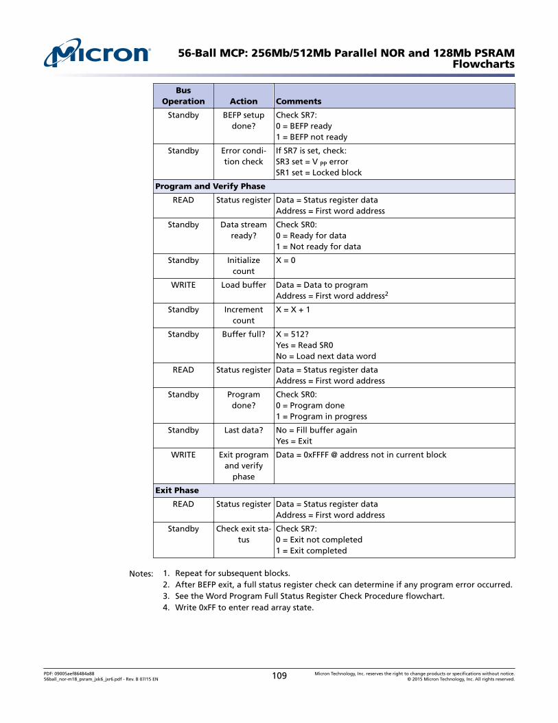
BusOperation Action Comments
Standby BEFP setupdone?
Check SR7:0 = BEFP ready1 = BEFP not ready
Standby Error condi-tion check
If SR7 is set, check:SR3 set = V PP errorSR1 set = Locked block
Program and Verify Phase
READ Status register Data = Status register dataAddress = First word address
Standby Data streamready?
Check SR0:0 = Ready for data1 = Not ready for data
Standby Initializecount
X = 0
WRITE Load buffer Data = Data to programAddress = First word address2
Standby Incrementcount
X = X + 1
Standby Buffer full? X = 512?Yes = Read SR0No = Load next data word
READ Status register Data = Status register dataAddress = First word address
Standby Programdone?
Check SR0:0 = Program done1 = Program in progress
Standby Last data? No = Fill buffer againYes = Exit
WRITE Exit programand verify
phase
Data = 0xFFFF @ address not in current block
Exit Phase
READ Status register Data = Status register dataAddress = First word address
Standby Check exit sta-tus
Check SR7:0 = Exit not completed1 = Exit completed
Notes: 1. Repeat for subsequent blocks.2. After BEFP exit, a full status register check can determine if any program error occurred.3. See the Word Program Full Status Register Check Procedure flowchart.4. Write 0xFF to enter read array state.
56-Ball MCP: 256Mb/512Mb Parallel NOR and 128Mb PSRAMFlowcharts
PDF: 09005aef86484a8856ball_nor-m18_psram_jxk6_jxr6.pdf - Rev. B 07/15 EN 109 Micron Technology, Inc. reserves the right to change products or specifications without notice.
© 2015 Micron Technology, Inc. All rights reserved.
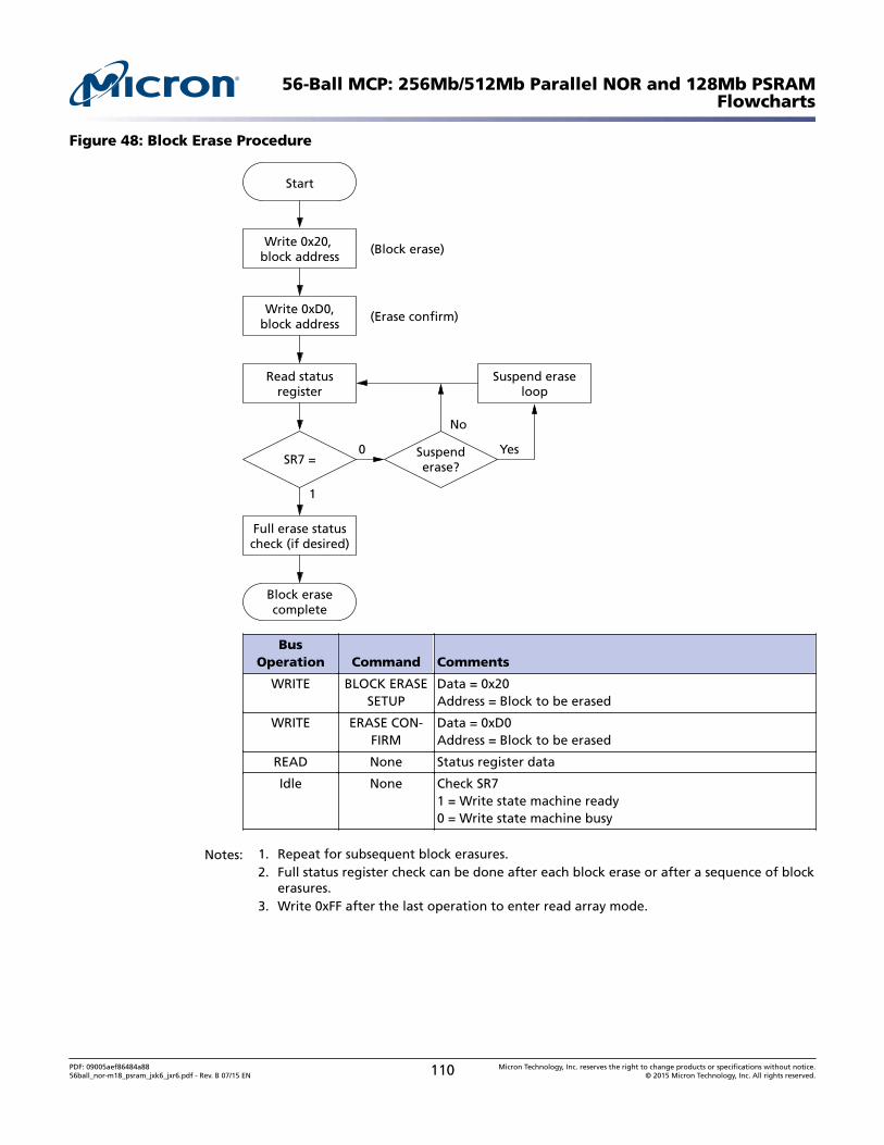
Figure 48: Block Erase Procedure
0
Block erasecomplete
1
SR7 =
Write 0x20, block address
Start
Write 0xD0,block address
(Block erase)
(Erase confirm)
Read statusregister
Suspend eraseloop
Yes
No
Suspenderase?
Full erase statuscheck (if desired)
BusOperation Command Comments
WRITE BLOCK ERASESETUP
Data = 0x20Address = Block to be erased
WRITE ERASE CON-FIRM
Data = 0xD0Address = Block to be erased
READ None Status register data
Idle None Check SR71 = Write state machine ready0 = Write state machine busy
Notes: 1. Repeat for subsequent block erasures.2. Full status register check can be done after each block erase or after a sequence of block
erasures.3. Write 0xFF after the last operation to enter read array mode.
56-Ball MCP: 256Mb/512Mb Parallel NOR and 128Mb PSRAMFlowcharts
PDF: 09005aef86484a8856ball_nor-m18_psram_jxk6_jxr6.pdf - Rev. B 07/15 EN 110 Micron Technology, Inc. reserves the right to change products or specifications without notice.
© 2015 Micron Technology, Inc. All rights reserved.
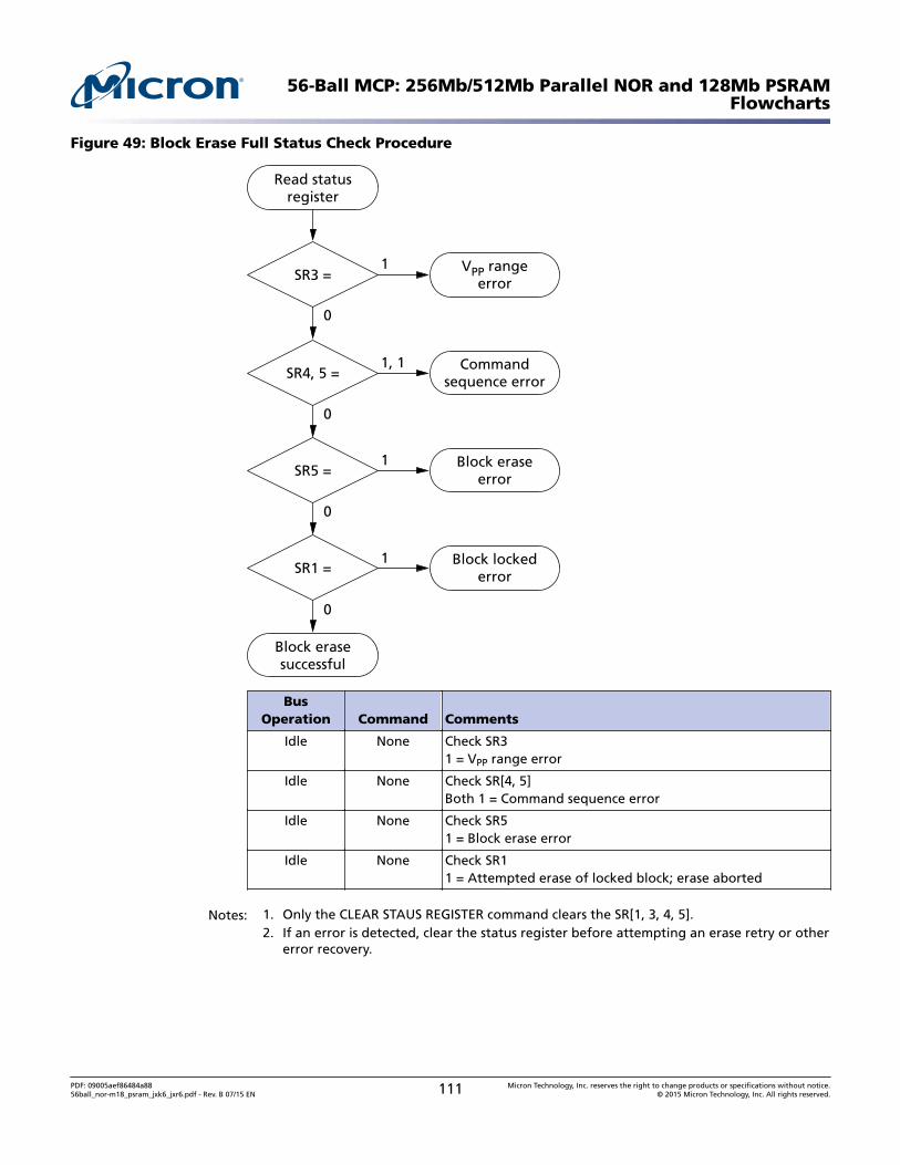
Figure 49: Block Erase Full Status Check Procedure
Block erasesuccessful
1
0
1, 1
0
1
0
Read statusregister
SR3 =
SR4, 5 =
SR1 =
Commandsequence error
1
0
SR5 =Block erase
error
Block lockederror
VPP rangeerror
BusOperation Command Comments
Idle None Check SR31 = VPP range error
Idle None Check SR[4, 5]Both 1 = Command sequence error
Idle None Check SR51 = Block erase error
Idle None Check SR11 = Attempted erase of locked block; erase aborted
Notes: 1. Only the CLEAR STAUS REGISTER command clears the SR[1, 3, 4, 5].2. If an error is detected, clear the status register before attempting an erase retry or other
error recovery.
56-Ball MCP: 256Mb/512Mb Parallel NOR and 128Mb PSRAMFlowcharts
PDF: 09005aef86484a8856ball_nor-m18_psram_jxk6_jxr6.pdf - Rev. B 07/15 EN 111 Micron Technology, Inc. reserves the right to change products or specifications without notice.
© 2015 Micron Technology, Inc. All rights reserved.
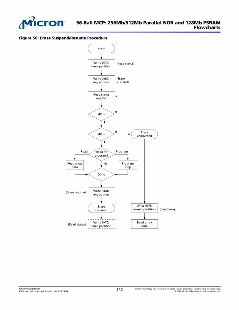
Figure 50: Erase Suspend/Resume Procedure
0
1
SR7 =
Write 0x70,same partition
Start
Write 0xB0,any address
(Erasesuspend)
(Read status)
ProgramRead
(Erase resume)
(Read status)
Write 0xD0,any address
Programloop
Read arraydata
Write 0x70,same partition
Write 0xFF,erased partition (Read array)
Read arraydata
Read statusregister
0
1
SR6 =
Eraseresumed
No
Done
Read orprogram?
Erasecompleted
56-Ball MCP: 256Mb/512Mb Parallel NOR and 128Mb PSRAMFlowcharts
PDF: 09005aef86484a8856ball_nor-m18_psram_jxk6_jxr6.pdf - Rev. B 07/15 EN 112 Micron Technology, Inc. reserves the right to change products or specifications without notice.
© 2015 Micron Technology, Inc. All rights reserved.

BusOperation Command Comments
WRITE READ STATUS Data = 0x70Address = Any partition address
WRITE ERASE SUS-PEND
Data = 0xB0Address = Same partition address as above
READ None Status register dataAddress = Same partition
Idle None Check SR71 = Write state machine ready0 = Write state machine busy
Idle None Check SR61 = Erase suspended0 = Erase completed
WRITE Any READ orPROGRAM
Data = Command for desired operationAddress = Any address within the suspended partition
READ orWRITE
None Read array or program data from/to block other than the onebeing erased
WRITE PROGRAM RE-SUME
Data = 0xD0Address = Any address
If the suspended partition was placed in read array mode or a program loop:
WRITE READ STATUSREGISTER
Return partition to status mode:Data = 0x70Address = Same partition
56-Ball MCP: 256Mb/512Mb Parallel NOR and 128Mb PSRAMFlowcharts
PDF: 09005aef86484a8856ball_nor-m18_psram_jxk6_jxr6.pdf - Rev. B 07/15 EN 113 Micron Technology, Inc. reserves the right to change products or specifications without notice.
© 2015 Micron Technology, Inc. All rights reserved.
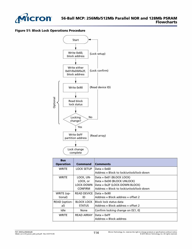
Figure 51: Block Lock Operations Procedure
No
Yes
Lockingchange?
Write 0x60,block address
Start
Write either0x01/0xD0/0x2F,
block address(Lock confirm)
(Read device ID)
(Lock setup)
(Read array)
Op
tio
nal
Write 0xFFpartition address
Write 0x90
Read blocklock status
Lock changecomplete
BusOperation Command Comments
WRITE LOCK SETUP Data = 0x60Address = Block to lock/unlock/lock-down
WRITE LOCK, UN-LOCK, or
LOCK-DOWNCONFIRM
Data = 0x01 (BLOCK LOCK)Data = 0xD0 (BLOCK UNLOCK)Data = 0x2F (LOCK-DOWN BLOCK)Address = Block to lock/unlock/lock-down
WRITE (op-tional)
READ DEVICEID
Data = 0x90Address = Block address + offset 2
READ (option-al)
BLOCK LOCKSTATUS
Block lock status dataAddress = Block address + offset 2
Idle None Confirm locking change on D[1, 0]
WRITE READ ARRAY Data = 0xFFAddress = Block address
56-Ball MCP: 256Mb/512Mb Parallel NOR and 128Mb PSRAMFlowcharts
PDF: 09005aef86484a8856ball_nor-m18_psram_jxk6_jxr6.pdf - Rev. B 07/15 EN 114 Micron Technology, Inc. reserves the right to change products or specifications without notice.
© 2015 Micron Technology, Inc. All rights reserved.
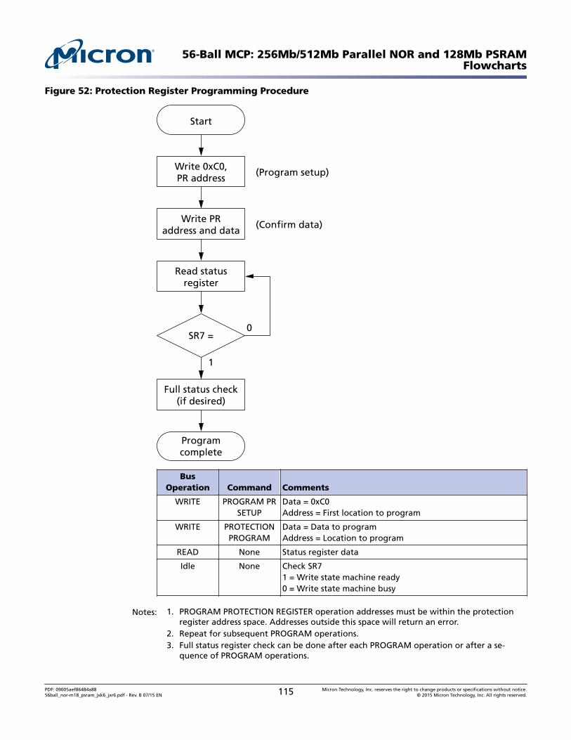
Figure 52: Protection Register Programming Procedure
0
Programcomplete
1
SR7 =
Write 0xC0,PR address
Start
Write PRaddress and data
(Program setup)
(Confirm data)
Read statusregister
Full status check(if desired)
BusOperation Command Comments
WRITE PROGRAM PRSETUP
Data = 0xC0Address = First location to program
WRITE PROTECTIONPROGRAM
Data = Data to programAddress = Location to program
READ None Status register data
Idle None Check SR71 = Write state machine ready0 = Write state machine busy
Notes: 1. PROGRAM PROTECTION REGISTER operation addresses must be within the protectionregister address space. Addresses outside this space will return an error.
2. Repeat for subsequent PROGRAM operations.3. Full status register check can be done after each PROGRAM operation or after a se-
quence of PROGRAM operations.
56-Ball MCP: 256Mb/512Mb Parallel NOR and 128Mb PSRAMFlowcharts
PDF: 09005aef86484a8856ball_nor-m18_psram_jxk6_jxr6.pdf - Rev. B 07/15 EN 115 Micron Technology, Inc. reserves the right to change products or specifications without notice.
© 2015 Micron Technology, Inc. All rights reserved.

4. Write 0xFF after the last operation to set to the read array state.
56-Ball MCP: 256Mb/512Mb Parallel NOR and 128Mb PSRAMFlowcharts
PDF: 09005aef86484a8856ball_nor-m18_psram_jxk6_jxr6.pdf - Rev. B 07/15 EN 116 Micron Technology, Inc. reserves the right to change products or specifications without notice.
© 2015 Micron Technology, Inc. All rights reserved.
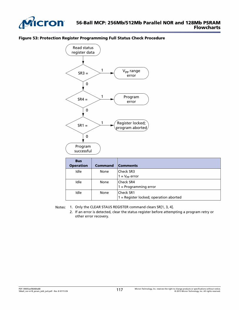
Figure 53: Protection Register Programming Full Status Check Procedure
Programsuccessful
1
0
1
0
1
0
Read statusregister data
SR3 =
SR4 =
SR1 =
Programerror
Register locked;program aborted
VPP rangeerror
BusOperation Command Comments
Idle None Check SR31 = VPP error
Idle None Check SR41 = Programming error
Idle None Check SR11 = Register locked; operation aborted
Notes: 1. Only the CLEAR STAUS REGISTER command clears SR[1, 3, 4].2. If an error is detected, clear the status register before attempting a program retry or
other error recovery.
56-Ball MCP: 256Mb/512Mb Parallel NOR and 128Mb PSRAMFlowcharts
PDF: 09005aef86484a8856ball_nor-m18_psram_jxk6_jxr6.pdf - Rev. B 07/15 EN 117 Micron Technology, Inc. reserves the right to change products or specifications without notice.
© 2015 Micron Technology, Inc. All rights reserved.
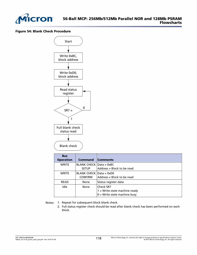
Figure 54: Blank Check Procedure
0
Blank check
1
SR7 =
Write 0xBC,block address
Start
Write 0xD0,block address
Read statusregister
Full blank checkstatus read
BusOperation Command Comments
WRITE BLANK CHECKSETUP
Data = 0xBCAddress = Block to be read
WRITE BLANK CHECKCONFIRM
Data = 0xD0Address = Block to be read
READ None Status register data
Idle None Check SR71 = Write state machine ready0 = Write state machine busy
Notes: 1. Repeat for subsequent block blank check.2. Full status register check should be read after blank check has been performed on each
block.
56-Ball MCP: 256Mb/512Mb Parallel NOR and 128Mb PSRAMFlowcharts
PDF: 09005aef86484a8856ball_nor-m18_psram_jxk6_jxr6.pdf - Rev. B 07/15 EN 118 Micron Technology, Inc. reserves the right to change products or specifications without notice.
© 2015 Micron Technology, Inc. All rights reserved.
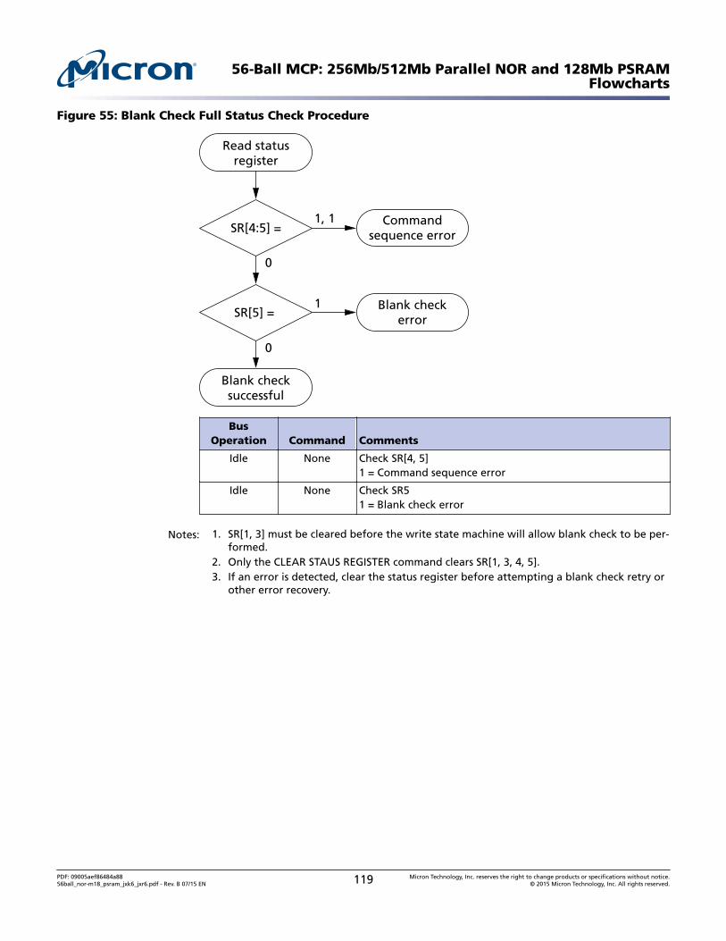
Figure 55: Blank Check Full Status Check Procedure
Blank checksuccessful
1, 1
0
1
0
Read statusregister
SR[4:5] =
SR[5] = Blank check
error
Commandsequence error
BusOperation Command Comments
Idle None Check SR[4, 5]1 = Command sequence error
Idle None Check SR51 = Blank check error
Notes: 1. SR[1, 3] must be cleared before the write state machine will allow blank check to be per-formed.
2. Only the CLEAR STAUS REGISTER command clears SR[1, 3, 4, 5].3. If an error is detected, clear the status register before attempting a blank check retry or
other error recovery.
56-Ball MCP: 256Mb/512Mb Parallel NOR and 128Mb PSRAMFlowcharts
PDF: 09005aef86484a8856ball_nor-m18_psram_jxk6_jxr6.pdf - Rev. B 07/15 EN 119 Micron Technology, Inc. reserves the right to change products or specifications without notice.
© 2015 Micron Technology, Inc. All rights reserved.
AADM Mode
AADM Feature Overview
The following is a list of general requirements for AADM mode.
Feature availability. AADM mode is available in devices that are configured as A/DMUX. With this configuration, AADM mode is enabled by setting a specific volatile bit inthe read configuration register.
High-address capture (A[MAX:16]). When AADM mode is enabled, A[MAX:16] andA[15:0] are captured from the A/ DQ[15:0] balls. The selection of A[MAX:16] or A[15:0] isdetermined by the state of the OE# input, as A[MAX:16] is captured when OE# is at VIL.
READ and WRITE cycle support. In AADM mode, both asynchronous and synchronouscycles are supported.
Customer requirements. For AADM operation, the customer is required to groundA[MAX:16].
Other characteristics. For AADM, all other device characteristics (program time, erasetime, ICCS, etc.) are the same as A/D MUX unless otherwise stated.
AADM Mode Enable (RCR[4] = 1)
Setting RCR[4] to its non-default state (1b) enables AADM mode. The default deviceconfiguration upon reset or power-up is A/D MUX mode. Upon setting RCR[4] = 1, theupper addresses, A[MAX:16] are latched. All 0s are latched by default.
Bus Cycles and Address Capture
+ AADM bus operations have one or two address cycles. For two address cycles, the up-per address (A[MAX:16]) must be issued first, followed by the lower address (A[15:0]).For bus operations with only one address cycle, only the lower address is issued. Theupper address that applies is the one that was most recently latched on a previous buscycle. For all READ cycles, sensing begins when the lower address is latched, regardlessof whether there are one or two address cycles.
In bus cycles, the external signal that distinguishes the upper address from the loweraddress is OE#. When OE# is at V IH, a lower address is captured; when OE# is at VIL, anupper address is captured.
When the bus cycle has only one address cycle, the timing waveform is similar to A/DMUX mode. The lower address is latched when OE# is at V IH, and data is subsequentlyoutputted after the falling edge of OE#.
When the device initially enters AADM mode, the upper address is internally latched asall 0s.
WAIT Behavior
The WAIT behavior in AADM mode functions the same as the legacy non-MUX WAITbehavior (A/D MUX WAIT behavior is unique). In other words, WAIT will always bedriven whenever DQ[15:0] is driven, and WAIT will tri-state whenever DQ[15:0] tri-state.
56-Ball MCP: 256Mb/512Mb Parallel NOR and 128Mb PSRAMAADM Mode
PDF: 09005aef86484a8856ball_nor-m18_psram_jxk6_jxr6.pdf - Rev. B 07/15 EN 120 Micron Technology, Inc. reserves the right to change products or specifications without notice.
© 2015 Micron Technology, Inc. All rights reserved.
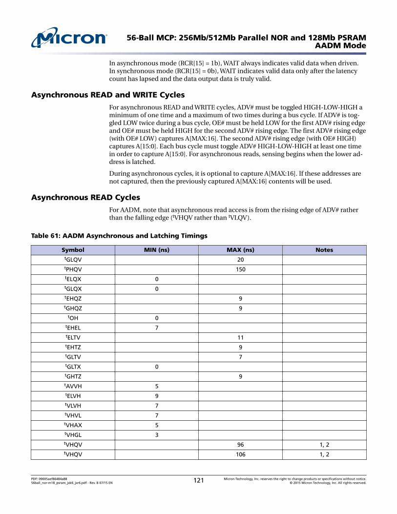
In asynchronous mode (RCR[15] = 1b), WAIT always indicates valid data when driven.In synchronous mode (RCR[15] = 0b), WAIT indicates valid data only after the latencycount has lapsed and the data output data is truly valid.
Asynchronous READ and WRITE Cycles
For asynchronous READ and WRITE cycles, ADV# must be toggled HIGH-LOW-HIGH aminimum of one time and a maximum of two times during a bus cycle. If ADV# is tog-gled LOW twice during a bus cycle, OE# must be held LOW for the first ADV# rising edgeand OE# must be held HIGH for the second ADV# rising edge. The first ADV# rising edge(with OE# LOW) captures A[MAX:16]. The second ADV# rising edge (with OE# HIGH)captures A[15:0]. Each bus cycle must toggle ADV# HIGH-LOW-HIGH at least one timein order to capture A[15:0]. For asynchronous reads, sensing begins when the lower ad-dress is latched.
During asynchronous cycles, it is optional to capture A[MAX:16]. If these addresses arenot captured, then the previously captured A[MAX:16] contents will be used.
Asynchronous READ Cycles
For AADM, note that asynchronous read access is from the rising edge of ADV# ratherthan the falling edge (tVHQV rather than tVLQV).
Table 61: AADM Asynchronous and Latching Timings
Symbol MIN (ns) MAX (ns) NotestGLQV 20 tPHQV 150 tELQX 0 tGLQX 0 tEHQZ 9 tGHQZ 9
tOH 0 tEHEL 7 tELTV 11 tEHTZ 9 tGLTV 7 tGLTX 0 tGHTZ 9 tAVVH 5 tELVH 9 tVLVH 7 tVHVL 7 tVHAX 5 tVHGL 3 tVHQV 96 1, 2tVHQV 106 1, 2
56-Ball MCP: 256Mb/512Mb Parallel NOR and 128Mb PSRAMAADM Mode
PDF: 09005aef86484a8856ball_nor-m18_psram_jxk6_jxr6.pdf - Rev. B 07/15 EN 121 Micron Technology, Inc. reserves the right to change products or specifications without notice.
© 2015 Micron Technology, Inc. All rights reserved.
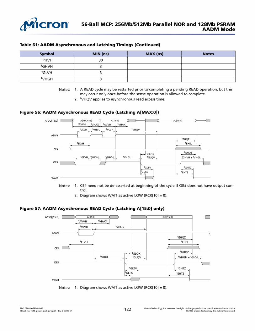
Table 61: AADM Asynchronous and Latching Timings (Continued)
Symbol MIN (ns) MAX (ns) NotestPHVH 30 tGHVH 3 tGLVH 3 tVHGH 3
Notes: 1. A READ cycle may be restarted prior to completing a pending READ operation, but thismay occur only once before the sense operation is allowed to complete.
2. tVHQV applies to asynchronous read access time.
Figure 56: AADM Asynchronous READ Cycle (Latching A[MAX:0])
A/DQ[15:0]
ADV#
CE#
OE#
WAIT
tVLVH tVHVL
tAVVH tAVVH tVHAX
tELVH
tGLTV
tGLVH tVHGH tGHVH tVHGL
tGHTZ
tEHTZ
tGHQZ
tGHVH + tVHGL
tGLQXtGLQV
tEHQZtEHEL
tVLVH tVHQV
tVHAX
tGLTX
A[MAX:16] A[15:0] DQ[15:0]
Notes: 1. CE# need not be de-asserted at beginning of the cycle if OE# does not have output con-trol.
2. Diagram shows WAIT as active LOW (RCR[10] = 0).
Figure 57: AADM Asynchronous READ Cycle (Latching A[15:0] only)
A/DQ[15:0]
ADV#
CE#
OE#
WAIT
tAVVH tVHAX
tELVH
tGLTV
tVHGL
tGHTZ
tEHTZ
tGHQZ
tVHGH + tGHVL
tGLQXtGLQV
tEHQZtEHEL
tVLVH tVHQV
tGLTX
A[15:0] DQ[15:0]
Notes: 1. Diagram shows WAIT as active LOW (RCR[10] = 0).
56-Ball MCP: 256Mb/512Mb Parallel NOR and 128Mb PSRAMAADM Mode
PDF: 09005aef86484a8856ball_nor-m18_psram_jxk6_jxr6.pdf - Rev. B 07/15 EN 122 Micron Technology, Inc. reserves the right to change products or specifications without notice.
© 2015 Micron Technology, Inc. All rights reserved.
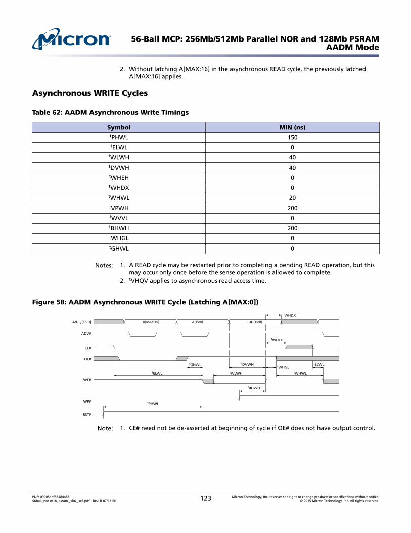
2. Without latching A[MAX:16] in the asynchronous READ cycle, the previously latchedA[MAX:16] applies.
Asynchronous WRITE Cycles
Table 62: AADM Asynchronous Write Timings
Symbol MIN (ns)tPHWL 150tELWL 0
tWLWH 40tDVWH 40tWHEH 0tWHDX 0tWHWL 20tVPWH 200tWVVL 0tBHWH 200tWHGL 0tGHWL 0
Notes: 1. A READ cycle may be restarted prior to completing a pending READ operation, but thismay occur only once before the sense operation is allowed to complete.
2. tVHQV applies to asynchronous read access time.
Figure 58: AADM Asynchronous WRITE Cycle (Latching A[MAX:0])
A/DQ[15:0]
ADV#
CE#
OE#
tWHWL
tDVWH tWHGLtWLWH
tBHWH
tGHWL tELWL
tWHDX
tELWL
tWHEH
WE#
WP#
RST#
tPHWL
A[MAX:16] A[15:0] DQ[15:0]
Note: 1. CE# need not be de-asserted at beginning of cycle if OE# does not have output control.
56-Ball MCP: 256Mb/512Mb Parallel NOR and 128Mb PSRAMAADM Mode
PDF: 09005aef86484a8856ball_nor-m18_psram_jxk6_jxr6.pdf - Rev. B 07/15 EN 123 Micron Technology, Inc. reserves the right to change products or specifications without notice.
© 2015 Micron Technology, Inc. All rights reserved.
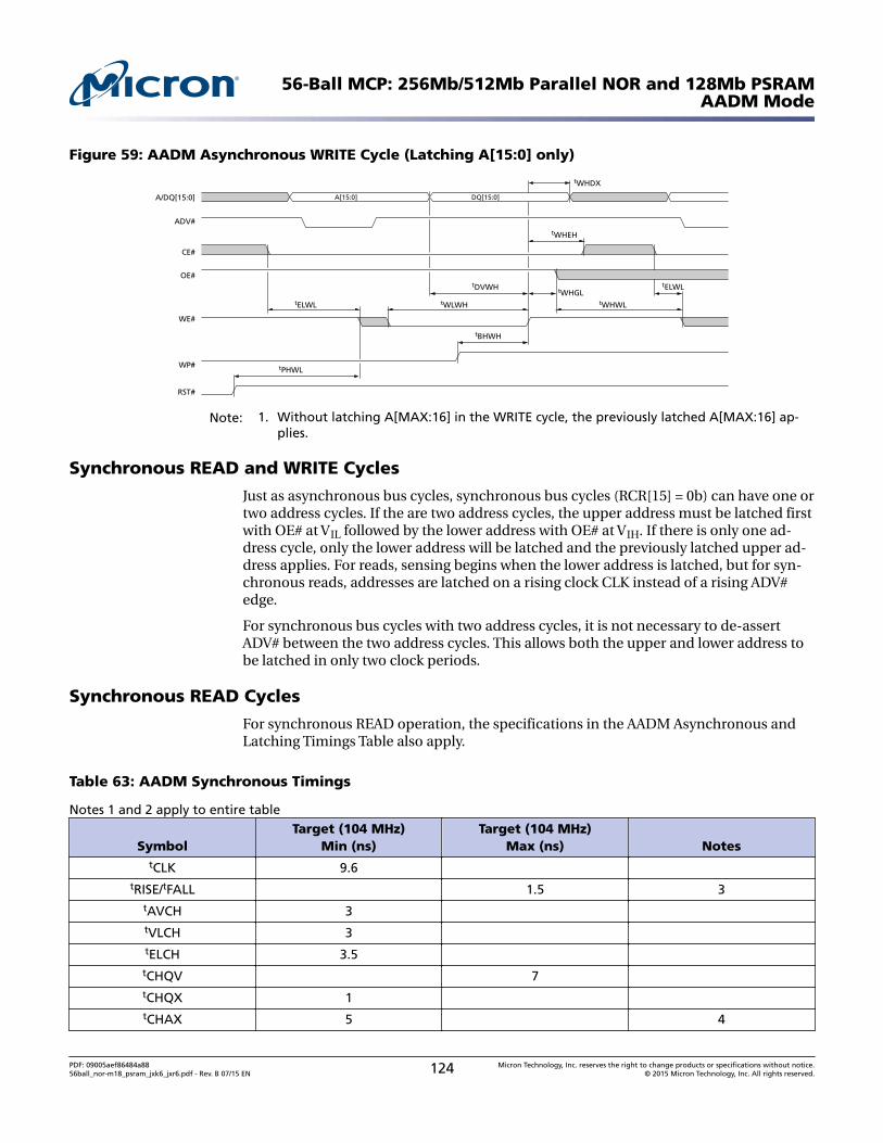
Figure 59: AADM Asynchronous WRITE Cycle (Latching A[15:0] only)
A/DQ[15:0]
ADV#
CE#
OE#
tWHWL
tDVWH tWHGLtWLWH
tBHWH
tELWL
tWHDX
tELWL
tWHEH
WE#
WP#
RST#
tPHWL
A[15:0] DQ[15:0]
Note: 1. Without latching A[MAX:16] in the WRITE cycle, the previously latched A[MAX:16] ap-plies.
Synchronous READ and WRITE Cycles
Just as asynchronous bus cycles, synchronous bus cycles (RCR[15] = 0b) can have one ortwo address cycles. If the are two address cycles, the upper address must be latched firstwith OE# at VIL followed by the lower address with OE# at VIH. If there is only one ad-dress cycle, only the lower address will be latched and the previously latched upper ad-dress applies. For reads, sensing begins when the lower address is latched, but for syn-chronous reads, addresses are latched on a rising clock CLK instead of a rising ADV#edge.
For synchronous bus cycles with two address cycles, it is not necessary to de-assertADV# between the two address cycles. This allows both the upper and lower address tobe latched in only two clock periods.
Synchronous READ Cycles
For synchronous READ operation, the specifications in the AADM Asynchronous andLatching Timings Table also apply.
Table 63: AADM Synchronous Timings
Notes 1 and 2 apply to entire table
SymbolTarget (104 MHz)
Min (ns)Target (104 MHz)
Max (ns) NotestCLK 9.6
tRISE/tFALL 1.5 3tAVCH 3 tVLCH 3 tELCH 3.5 tCHQV 7 tCHQX 1 tCHAX 5 4
56-Ball MCP: 256Mb/512Mb Parallel NOR and 128Mb PSRAMAADM Mode
PDF: 09005aef86484a8856ball_nor-m18_psram_jxk6_jxr6.pdf - Rev. B 07/15 EN 124 Micron Technology, Inc. reserves the right to change products or specifications without notice.
© 2015 Micron Technology, Inc. All rights reserved.
Table 63: AADM Synchronous Timings (Continued)
Notes 1 and 2 apply to entire table
SymbolTarget (104 MHz)
Min (ns)Target (104 MHz)
Max (ns) NotestCHTV 7 tCHVL 2.5 tCHTX 1 tCHVH 2 tCHGL 2.5 6, 4tVLVH tCLK 2 × tCLK 5, 6tVHCH 3 tCHGH 2 tGHCH 2 tGLCH 3
Notes: 1. In synchronous burst READ cycles, the asynchronous OE# to ADV# setup and hold timesmust also be met (tGHVH and tVHGL) to signify that the address capture phase of thebus cycle is complete.
2. A READ cycle may only be terminated (prior to the completion of sensing data) one timebefore a full bus cycle must be allowed to complete.
3. Rise and fall time specified between VIL and VIH.4. To prevent A/D bus contention between the host and the memory device, OE# may only
be asserted LOW after the host has satisfied the ADDR hold spec, tCHAX.5. The device must operate down to 9.6 MHz in synchronous burst mode.6. During the address capture phase of a read burst bus cycle, OE# timings relative to CLK
shall be identical to those of ADV# relative to CLK.
56-Ball MCP: 256Mb/512Mb Parallel NOR and 128Mb PSRAMAADM Mode
PDF: 09005aef86484a8856ball_nor-m18_psram_jxk6_jxr6.pdf - Rev. B 07/15 EN 125 Micron Technology, Inc. reserves the right to change products or specifications without notice.
© 2015 Micron Technology, Inc. All rights reserved.
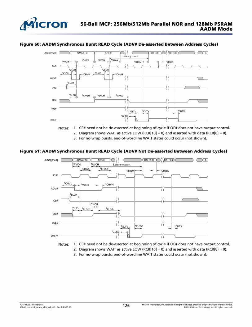
Figure 60: AADM Synchronous Burst READ Cycle (ADV# De-asserted Between Address Cycles)
A/DQ[15:0]
ADV#
CE#
OE#
WE#
WAIT
tCHVL
tVLCH
tAVCHtAVCH tCHAX tCHQX
tELCH
tGLTV tCHTV
tGLCH tCHGH tGHCH tCHGL
tCHTX
tCHQVtCHAX
tGLTX
A[MAX:16] AA[15:0] DQ[15:0]DQ[15:0]
CLK
tCHVHtCHVL
tVLCH
tCHVH
Latency count
Notes: 1. CE# need not be de-asserted at beginning of cycle if OE# does not have output control.2. Diagram shows WAIT as active LOW (RCR[10] = 0) and asserted with data (RCR[8] = 0).3. For no-wrap bursts, end-of-wordline WAIT states could occur (not shown).
Figure 61: AADM Synchronous Burst READ Cycle (ADV# Not De-asserted Between Address Cycles)
A/DQ[15:0]
ADV#
CE#
OE#
WE#
WAIT
tCHVL tVLCH
tAVCH tAVCHtCHAX tCHQX
tELCH
tGLTV tCHTV
tGLCH tCHGH
tGHCHtCHGL
tCHTX
tCHQVtCHAX
tGLTX
A[MAX:16] AA[15:0] DQ[15:0]DQ[15:0]
CLK
tCHVH
Latency count
Notes: 1. CE# need not be de-asserted at beginning of cycle if OE# does not have output control.2. Diagram shows WAIT as active LOW (RCR[10] = 0) and asserted with data (RCR[8] = 0).3. For no-wrap bursts, end-of-wordline WAIT states could occur (not shown).
56-Ball MCP: 256Mb/512Mb Parallel NOR and 128Mb PSRAMAADM Mode
PDF: 09005aef86484a8856ball_nor-m18_psram_jxk6_jxr6.pdf - Rev. B 07/15 EN 126 Micron Technology, Inc. reserves the right to change products or specifications without notice.
© 2015 Micron Technology, Inc. All rights reserved.
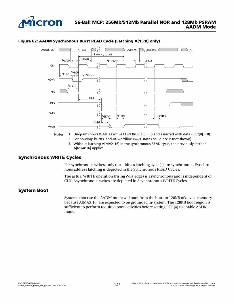
Figure 62: AADM Synchronous Burst READ Cycle (Latching A[15:0] only)
A/DQ[15:0]
ADV#
CE#
OE#
WE#
WAIT
tCHVLtVLCH
tAVCHtCHAX tCHQX
tELCH
tGLTV tCHTV
tCHGL
tCHTX
tCHQV
tGLTX
AA[15:0] DQ[15:0]DQ[15:0]
CLK
tCHVH
Latency count
Notes: 1. Diagram shows WAIT as active LOW (RCR[10] = 0) and asserted with data (RCR[8] = 0).2. For no-wrap bursts, end-of-wordline WAIT states could occur (not shown).3. Without latching A[MAX:16] in the synchronous READ cycle, the previously latched
A[MAX:16] applies.
Synchronous WRITE Cycles
For synchronous writes, only the address latching cycle(s) are synchronous. Synchro-nous address latching is depicted in the Synchronous READ Cycles.
The actual WRITE operation (rising WE# edge) is asynchronous and is independent ofCLK. Asynchronous writes are depicted in Asynchronous WRITE Cycles.
System Boot
Systems that use the AADM mode will boot from the bottom 128KB of device memorybecause A[MAX:16] are expected to be grounded in-system. The 128KB boot region issufficient to perform required boot activities before setting RCR[4] to enable AADMmode.
56-Ball MCP: 256Mb/512Mb Parallel NOR and 128Mb PSRAMAADM Mode
PDF: 09005aef86484a8856ball_nor-m18_psram_jxk6_jxr6.pdf - Rev. B 07/15 EN 127 Micron Technology, Inc. reserves the right to change products or specifications without notice.
© 2015 Micron Technology, Inc. All rights reserved.
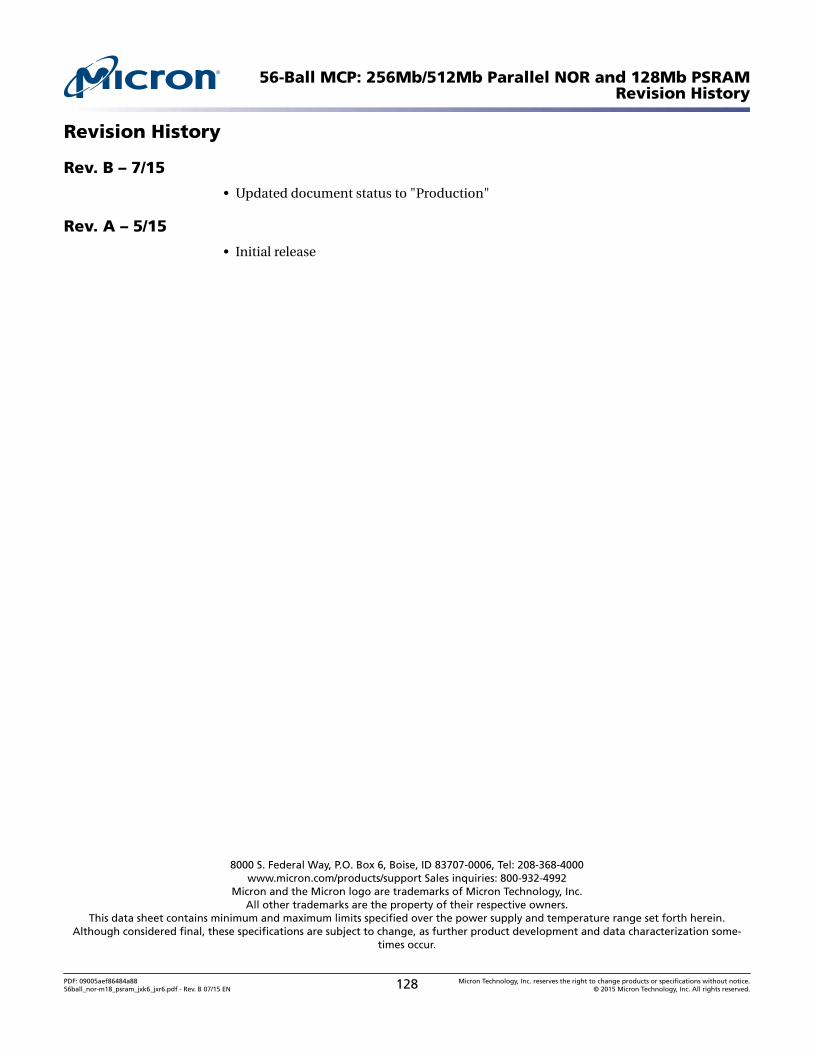
Revision History
Rev. B – 7/15
• Updated document status to "Production"
Rev. A – 5/15
• Initial release
8000 S. Federal Way, P.O. Box 6, Boise, ID 83707-0006, Tel: 208-368-4000www.micron.com/products/support Sales inquiries: 800-932-4992
Micron and the Micron logo are trademarks of Micron Technology, Inc.All other trademarks are the property of their respective owners.
This data sheet contains minimum and maximum limits specified over the power supply and temperature range set forth herein.Although considered final, these specifications are subject to change, as further product development and data characterization some-
times occur.
56-Ball MCP: 256Mb/512Mb Parallel NOR and 128Mb PSRAMRevision History
PDF: 09005aef86484a8856ball_nor-m18_psram_jxk6_jxr6.pdf - Rev. B 07/15 EN 128 Micron Technology, Inc. reserves the right to change products or specifications without notice.
© 2015 Micron Technology, Inc. All rights reserved.