5420xL data sheet (English) - NPC · 5420xL series VCXO Module ICs with ... 5 pins) 110μm×80μm...
26
5420xL series VCXO Module ICs with Built-in Varicap SEIKO NPC CORPORATION - 1 OVERVIEW The 5420xL series are LV-PECL output VCXO ICs that provide a wide frequency pulling range. They employ bipolar oscillator circuit and recently developed varicap diode fabrication process that provides a low phase noise characteristic and a wide frequency pulling range without any external components. Current consumption of the 5420xL series is reduced, it contributes to reduction of power consumption in applications. FEATURES ▪ VCXO with recently developed varicap diode built-in ▪ -40 to +105°C operating temperature range ▪ Oscillator: Fundamental frequency oscillation ▪ Differential LV-PECL output ▪ Output frequency (f OUT ): 100 to 250MHz ▪ Output enable (OE) active selectable function ▪ Operating supply voltage range: 2.97 to 3.63V Selectable Hi-Active or Low-Active by bonding wire ▪ Oscillator frequency range (for fundamental oscillation): ▪ Output terminal on standby state 100 to 170MHz (BL version) OUT: V OH (DC), OUTN: V OL (DC) 150 to 200MHz (CL version) 200 to 250MHz (DL version) ▪ Wide frequency pulling range (typ) ±130ppm@BL version, V C =1.65±1.65V, f OUT =122.88MHz ( γ =330, C 0 =1.6pF) ±120ppm@CL version, V C =1.65±1.65V, f OUT =155.52MHz ( γ =330, C 0 =1.5pF) * DL version: TBD ▪ Low phase noise (typ): -125dBc/Hz@BL version, 1kHz Offset, f OUT =122.88MHz ( γ =330, C 0 =1.6pF) -155dBc/Hz@BL version, 10MHz Offset, f OUT =122.88MHz -125dBc/Hz@CL version, 1kHz Offset, f OUT =155.52MHz ( γ =330, C 0 =1.5pF) -155dBc/Hz@CL version, 10MHz Offset, f OUT =155.52MHz * DL version: TBD APPLICATIONS Base station, SONET/SDH, Ethernet, Fibre Channel, LTE SERIES CONFIGURATION Version Name Recommended operating frequency range (f OSC ) *1 [MHz] Output frequency (f OUT ) 5420BL 100MHz to 170MHz f OSC 5420CL 150MHz to 200MHz f OSC (5420DL) *2 200MHz to 250MHz f OSC *1. The recommended oscillation frequency is a yardstick value derived from the resonator used for NPC characteristics authentication. However, the oscillation frequency range is not guaranteed. Specifically, the characteristics can vary greatly due to resonator characteristics and mounting conditions, so the oscillation characteristics of components must be carefully evaluated. The recommended characteristics for the crystal element are: R 1 < 20Ω, C 0 < 1.5pF *2. The version name in parentheses has been developed. ORDERING INFORMATION Device Package Version name WF5420xL-4 Wafer form WF5420□L-4 CF5420xL-4 Chip form Oscillation frequency range B:100 ~170MHz C: 1 50 ~2 00MHz Form WF: Wafer form CF: Chip(Die) form
Transcript of 5420xL data sheet (English) - NPC · 5420xL series VCXO Module ICs with ... 5 pins) 110μm×80μm...
5420xL series VCXO Module ICs with Built-in Varicap
SEIKO NPC CORPORATION - 1
OVERVIEW The 5420xL series are LV-PECL output VCXO ICs that provide a wide frequency pulling range. They employ bipolar oscillator circuit and recently developed varicap diode fabrication process that provides a low phase noise characteristic and a wide frequency pulling range without any external components. Current consumption of the 5420xL series is reduced, it contributes to reduction of power consumption in applications.
FEATURES VCXO with recently developed varicap diode built-in -40 to +105°C operating temperature range Oscillator: Fundamental frequency oscillation Differential LV-PECL output Output frequency (fOUT): 100 to 250MHz Output enable (OE) active selectable function Operating supply voltage range: 2.97 to 3.63V Selectable Hi-Active or Low-Active by bonding wire Oscillator frequency range (for fundamental oscillation): Output terminal on standby state 100 to 170MHz (BL version) OUT: VOH (DC), OUTN: VOL (DC) 150 to 200MHz (CL version) 200 to 250MHz (DL version) Wide frequency pulling range (typ) ±130ppm@BL version, VC=1.65±1.65V, fOUT=122.88MHz (γ=330, C0=1.6pF) ±120ppm@CL version, VC=1.65±1.65V, fOUT=155.52MHz (γ=330, C0=1.5pF) * DL version: TBD Low phase noise (typ): -125dBc/Hz@BL version, 1kHz Offset, fOUT=122.88MHz (γ=330, C0=1.6pF) -155dBc/Hz@BL version, 10MHz Offset, fOUT=122.88MHz
-125dBc/Hz@CL version, 1kHz Offset, fOUT=155.52MHz (γ=330, C0=1.5pF) -155dBc/Hz@CL version, 10MHz Offset, fOUT=155.52MHz
* DL version: TBD APPLICATIONS Base station, SONET/SDH, Ethernet, Fibre Channel, LTE
SERIES CONFIGURATION
Version Name Recommended operating frequency range
(fOSC)*1 [MHz] Output frequency (fOUT)
5420BL 100MHz to 170MHz fOSC
5420CL 150MHz to 200MHz fOSC
(5420DL)*2 200MHz to 250MHz fOSC *1. The recommended oscillation frequency is a yardstick value derived from the resonator used for NPC characteristics authentication. However, the
oscillation frequency range is not guaranteed. Specifically, the characteristics can vary greatly due to resonator characteristics and mounting conditions, so the oscillation characteristics of components must be carefully evaluated.
The recommended characteristics for the crystal element are: R1 < 20Ω, C0 < 1.5pF *2. The version name in parentheses has been developed.
ORDERING INFORMATION
Device Package Version name
WF5420xL-4 Wafer form WF5420L-4
CF5420xL-4 Chip form Oscillation frequency range B:100~170MHz C:150~200MHz
Form WF: Wafer form CF: Chip(Die) form
5420xL series
SEIKO NPC CORPORATION - 2
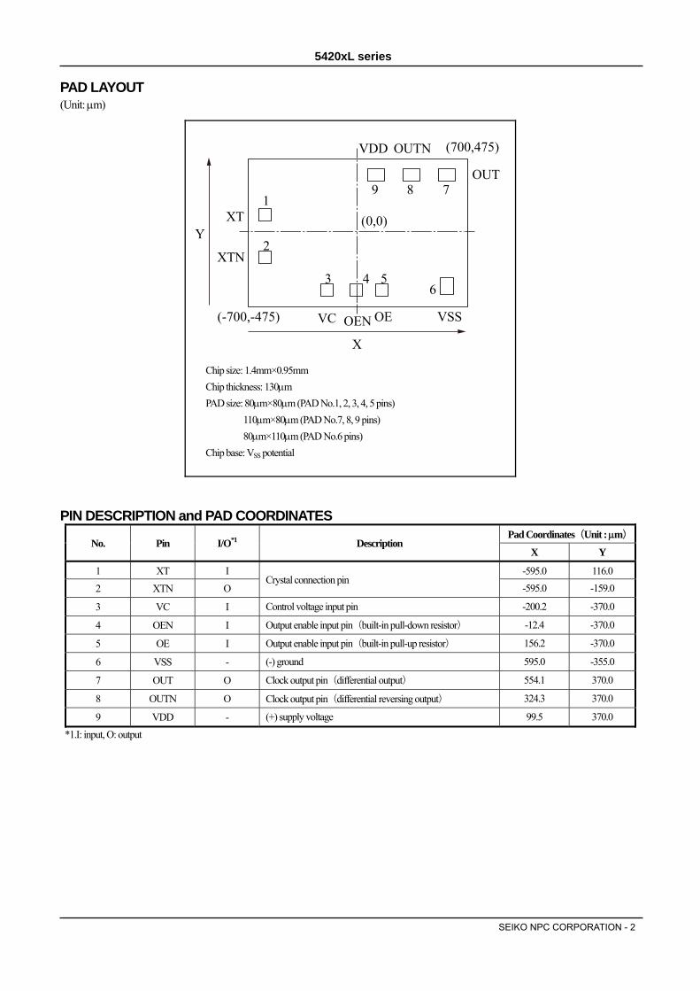
PAD LAYOUT (Unit: μm)
PIN DESCRIPTION and PAD COORDINATES
No. Pin I/O*1 Description Pad Coordinates (Unit : μm)
X Y
1 XT I Crystal connection pin
-595.0 116.0
2 XTN O -595.0 -159.0
3 VC I Control voltage input pin -200.2 -370.0
4 OEN I Output enable input pin (built-in pull-down resistor) -12.4 -370.0
5 OE I Output enable input pin (built-in pull-up resistor) 156.2 -370.0
6 VSS - (-) ground 595.0 -355.0
7 OUT O Clock output pin (differential output) 554.1 370.0
8 OUTN O Clock output pin (differential reversing output) 324.3 370.0
9 VDD - (+) supply voltage 99.5 370.0
*1.I: input, O: output
Chip size: 1.4mm×0.95mm Chip thickness: 130μm PAD size: 80μm×80μm (PAD No.1, 2, 3, 4, 5 pins) 110μm×80μm (PAD No.7, 8, 9 pins)
80μm×110μm (PAD No.6 pins) Chip base: VSS potential
YXT
XTN
OUT
OUTNVDD
1
2
3 4 56
789
(700,475)
(0,0)
(-700,-475)
X
VC OEN OE VSS
5420xL series
SEIKO NPC CORPORATION - 3
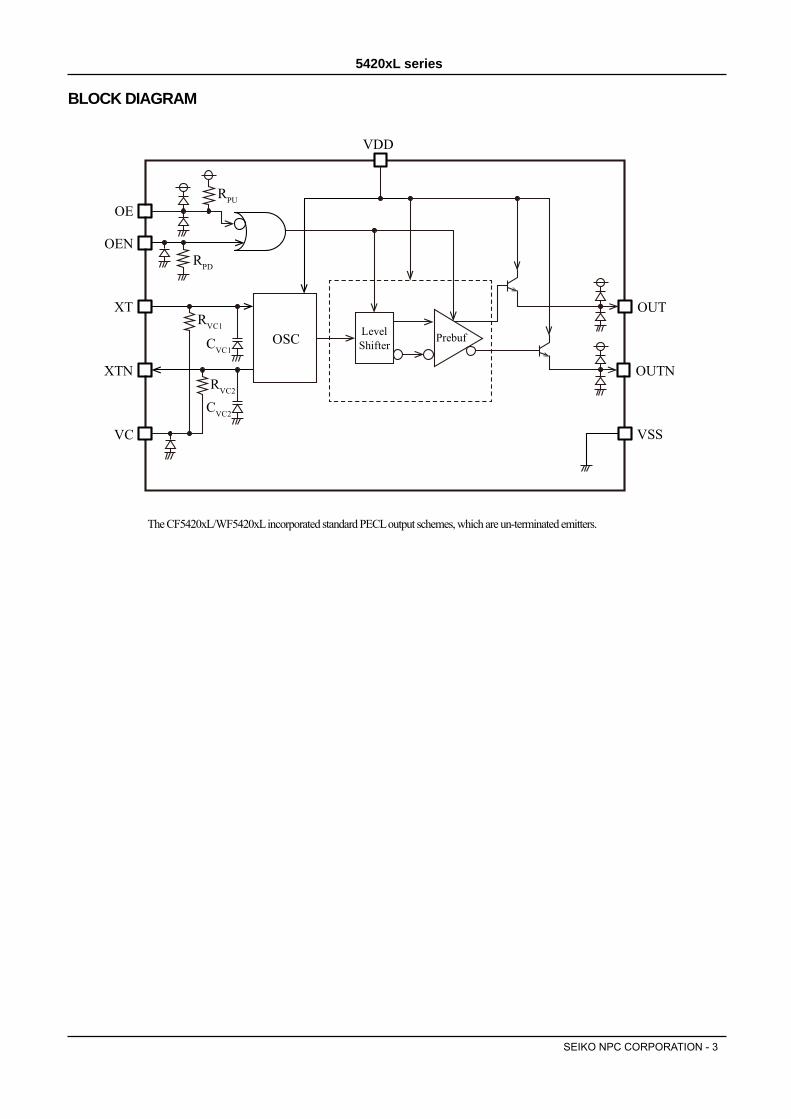
BLOCK DIAGRAM
The CF5420xL/WF5420xL incorporated standard PECL output schemes, which are un-terminated emitters.
RPU
RPD
RVC1
CVC1
RVC2
CVC2
OSC LevelShifter
Prebuf
OUT
OUTN
VSS
VDD
OE
OEN
XT
XTN
VC
5420xL series
SEIKO NPC CORPORATION - 4
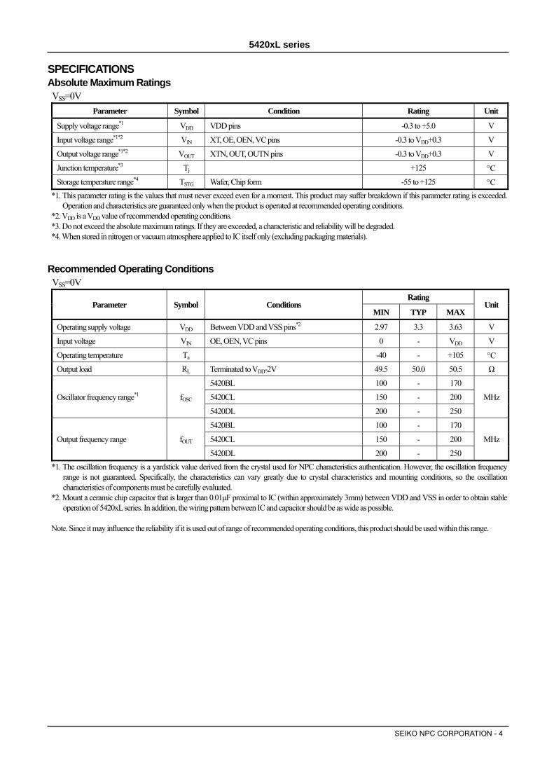
SPECIFICATIONS Absolute Maximum Ratings VSS=0V
Parameter Symbol Condition Rating Unit
Supply voltage range*1 VDD VDD pins -0.3 to +5.0 V
Input voltage range*1*2 VIN XT, OE, OEN, VC pins -0.3 to VDD+0.3 V
Output voltage range*1*2 VOUT XTN, OUT, OUTN pins -0.3 to VDD+0.3 V
Junction temperature*3 Tj +125 °C Storage temperature range*4 TSTG Wafer, Chip form -55 to +125 °C
*1. This parameter rating is the values that must never exceed even for a moment. This product may suffer breakdown if this parameter rating is exceeded. Operation and characteristics are guaranteed only when the product is operated at recommended operating conditions.
*2. VDD is a VDD value of recommended operating conditions. *3. Do not exceed the absolute maximum ratings. If they are exceeded, a characteristic and reliability will be degraded. *4. When stored in nitrogen or vacuum atmosphere applied to IC itself only (excluding packaging materials). Recommended Operating Conditions VSS=0V
Parameter Symbol Conditions Rating
Unit MIN TYP MAX
Operating supply voltage VDD Between VDD and VSS pins*2 2.97 3.3 3.63 V
Input voltage VIN OE, OEN, VC pins 0 - VDD V
Operating temperature Ta -40 - +105 °C Output load RL Terminated to VDD-2V 49.5 50.0 50.5 Ω
Oscillator frequency range*1 fOSC
5420BL 100 - 170
MHz 5420CL 150 - 200
5420DL 200 - 250
Output frequency range fOUT
5420BL 100 - 170
MHz 5420CL 150 - 200
5420DL 200 - 250 *1. The oscillation frequency is a yardstick value derived from the crystal used for NPC characteristics authentication. However, the oscillation frequency
range is not guaranteed. Specifically, the characteristics can vary greatly due to crystal characteristics and mounting conditions, so the oscillation characteristics of components must be carefully evaluated.
*2. Mount a ceramic chip capacitor that is larger than 0.01μF proximal to IC (within approximately 3mm) between VDD and VSS in order to obtain stable operation of 5420xL series. In addition, the wiring pattern between IC and capacitor should be as wide as possible.
Note. Since it may influence the reliability if it is used out of range of recommended operating conditions, this product should be used within this range.
5420xL series
SEIKO NPC CORPORATION - 5
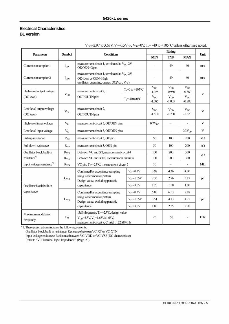
Electrical Characteristics BL version VDD=2.97 to 3.63V, VC=0.5VDD, VSS=0V, Ta= -40 to +105°C unless otherwise noted.
Parameter Symbol Conditions Rating
Unit MIN TYP MAX
Current consumption1 IDD1 measurement circuit 1, terminated to VDD-2V, OE,OEN=Open - 49 60 mA
Current consumption2 IDD2 measurement circuit 1, terminated to VDD-2V, OE=Low or OEN=High oscillator: operating, output: DC(VOH, VOL)
- 49 60 mA
High-level output voltage (DC level)
VOH measurement circuit 2, OUT/OUTN pins
Ta=0 to +105°C VDD
-1.025 VDD
-0.950 VDD
-0.880 V Ta=-40 to 0°C VDD
-1.085 VDD
-1.005 VDD
-0.880
Low-level output voltage (DC level)
VOL measurement circuit 2, OUT/OUTN pins
VDD
-1.810 VDD
-1.700 VDD
-1.620 V
High-level input voltage VIH measurement circuit 3, OE/OEN pins 0.7VDD - - V
Low-level input voltage VIL measurement circuit 3, OE/OEN pins - - 0.3VDD V
Pull-up resistance RPU measurement circuit 3, OE pin 50 100 200 kΩ
Pull-down resistance RPD measurement circuit 3, OEN pin 50 100 200 kΩ
Oscillator block built-in resistance*1
RVC1 Between VC and XT, measurement circuit 4 100 200 300 kΩ
RVC2 Between VC and XTN, measurement circuit 4 100 200 300
Input leakage resistance*1 RVIN VC pin, Ta=+25°C, measurement circuit 5 10 - - MΩ
Oscillator block built-in capacitance
CVC1
Confirmed by acceptance sampling using wafer monitor pattern. Design value, excluding parasitic capacitance
VC =0.3V 3.92 4.36 4.80
pF VC =1.65V 2.35 2.76 3.17
VC =3.0V 1.20 1.50 1.80
CVC2
Confirmed by acceptance sampling using wafer monitor pattern. Design value, excluding parasitic capacitance
VC =0.3V 5.88 6.53 7.18
pF VC =1.65V 3.51 4.13 4.75
VC =3.0V 1.80 2.25 2.70
Maximum modulation frequency
FM -3dB frequency, Ta=+25°C, design value VDD=3.3V, VC=1.65V±1.65V, measurement circuit 8, Crystal : 122.88MHz
25 50 - kHz
*1. These prescriptions indicate the following contents. Oscillator block built-in resistance: Resistance between VC-XT or VC-XTN Input leakage resistance: Resistance between VC-VDD or VC-VSS (DC characteristic) Refer to “VC Terminal Input Impedance”. (Page. 23)
5420xL series
SEIKO NPC CORPORATION - 6
CL version VDD=2.97 to 3.63V, VC=0.5VDD, VSS=0V, Ta= -40 to +105°C unless otherwise noted.
Parameter Symbol Conditions Rating
Unit MIN TYP MAX
Current consumption1 IDD1 measurement circuit 1, terminated to VDD-2V, OE,OEN=Open - 50 60 mA
Current consumption2 IDD2 measurement circuit 1, terminated to VDD-2V, OE=Low or OEN=High oscillator: operating, output: DC(VOH, VOL)
- 50 60 mA
High-level output voltage (DC level)
VOH measurement circuit 2, OUT/OUTN pins
Ta=0 to +105°C VDD
-1.025 VDD
-0.950 VDD
-0.880 V Ta=-40 to 0°C VDD
-1.085 VDD
-1.005 VDD
-0.880
Low-level output voltage (DC level)
VOL measurement circuit 2, OUT/OUTN pins
VDD
-1.810 VDD
-1.700 VDD
-1.620 V
High-level input voltage VIH measurement circuit 3, OE/OEN pins 0.7VDD - - V
Low-level input voltage VIL measurement circuit 3, OE/OEN pins - - 0.3VDD V
Pull-up resistance RPU measurement circuit 3, OE pin 50 100 200 kΩ
Pull-down resistance RPD measurement circuit 3, OEN pin 50 100 200 kΩ
Oscillator block built-in resistance*1
RVC1 Between VC and XT, measurement circuit 4 100 200 300 kΩ
RVC2 Between VC and XTN, measurement circuit 4 100 200 300
Input leakage resistance*1 RVIN VC pin, Ta=+25°C, measurement circuit 5 10 - - MΩ
Oscillator block built-in capacitance
CVC1
Confirmed by acceptance sampling using wafer monitor pattern. Design value, excluding parasitic capacitance
VC =0.3V 3.92 4.36 4.80
pF VC =1.65V 2.35 2.76 3.17
VC =3.0V 1.20 1.50 1.80
CVC2
Confirmed by acceptance sampling using wafer monitor pattern. Design value, excluding parasitic capacitance
VC =0.3V 5.88 6.53 7.18
pF VC =1.65V 3.51 4.13 4.75
VC =3.0V 1.80 2.25 2.70
Maximum modulation frequency
FM -3dB frequency, Ta=+25°C, design value VDD=3.3V, VC=1.65V±1.65V, measurement circuit 8, Crystal : 155.52MHz
25 50 - kHz
*1. These prescriptions indicate the following contents. Oscillator block built-in resistance: Resistance between VC-XT or VC-XTN Input leakage resistance: Resistance between VC-VDD or VC-VSS (DC characteristic) Refer to “VC Terminal Input Impedance” (Page. 23).
5420xL series
SEIKO NPC CORPORATION - 7
DL version (TBD) VDD=2.97 to 3.63V, VC=0.5VDD, VSS=0V, Ta= -40 to +105°C unless otherwise noted.
Parameter Symbol Conditions Rating
Unit MIN TYP MAX
Current consumption1 IDD1 measurement circuit 1, terminated to VDD-2V, OE,OEN=Open - (54) (75) mA
Current consumption2 IDD2 measurement circuit 1, terminated to VDD-2V, OE=Low or OEN=High oscillator: operating, output: DC(VOH, VOL)
- (54) (75) mA
High-level output voltage (DC level)
VOH measurement circuit 2, OUT/OUTN pins
Ta=0 to +105°C VDD
-1.025 VDD
-0.950 VDD
-0.880 V Ta=-40 to 0°C VDD
-1.085 VDD
-1.005 VDD
-0.880
Low-level output voltage (DC level)
VOL measurement circuit 2, OUT/OUTN pins
VDD
-1.810 VDD
-1.700 VDD
-1.620 V
High-level input voltage VIH measurement circuit 3, OE/OEN pins 0.7VDD - - V
Low-level input voltage VIL measurement circuit 3, OE/OEN pins - - 0.3VDD V
Pull-up resistance RPU measurement circuit 3, OE pin 50 100 200 kΩ
Pull-down resistance RPD measurement circuit 3, OEN pin 50 100 200 kΩ
Oscillator block built-in resistance*1
RVC1 Between VC and XT, measurement circuit 4 100 200 300 kΩ
RVC2 Between VC and XTN, measurement circuit 4 100 200 300
Input leakage resistance*1 RVIN VC pin, Ta=+25°C, measurement circuit 5 10 - - MΩ
Oscillator block built-in capacitance
CVC1
Confirmed by acceptance sampling using wafer monitor pattern. Design value, excluding parasitic capacitance
VC =0.3V (3.92) (4.36) (4.80)
pF VC =1.65V (2.35) (2.76) (3.17)
VC =3.0V (1.20) (1.50) (1.80)
CVC2
Confirmed by acceptance sampling using wafer monitor pattern. Design value, excluding parasitic capacitance
VC =0.3V (5.88) (6.53) (7.18)
pF VC =1.65V (3.51) (4.13) (4.75)
VC =3.0V (1.80) (2.25) (2.70)
Maximum modulation frequency
FM -3dB frequency, Ta=+25°C, design value VDD=3.3V, VC=1.65V±1.65V, measurement circuit 8, Crystal : 245.76MHz
25 50 - kHz
Values in parentheses ( ) are temporary. *1. These prescriptions indicate the following contents. Oscillator block built-in resistance: Resistance between VC-XT or VC-XTN Input leakage resistance: Resistance between VC-VDD or VC-VSS (DC characteristic) Refer to “VC Terminal Input Impedance” (TBD) (Page. 23).
5420xL series
SEIKO NPC CORPORATION - 8
Switching Characteristics VDD = 2.97 to 3.63V, VC=0.5VDD, VSS= 0V, Ta = -40 to +105°C unless otherwise noted
Parameter Symbol Conditions Rating
Unit MIN TYP MAX
Duty cycle
Duty1 Measured at output cross point Ta=25°C,VDD=3.3V, measurement circuit 6
45 50 55 %
Duty2 Measured at 50% of output amplitude Ta=25°C,VDD=3.3V, measurement circuit 6
45 50 55 %
Output amplitude VOPP Peak to peak of output waveform Single-ended output signal, measurement circuit 6
0.4 - - V
Output rise time*1 tr 20% to 80% of output amplitude Single-ended output signal, measurement circuit 6
-40 to 90°C - 0.3 0.5 ns
90 to 105°C - - 0.7
Output fall time*1 tf 80% to 20% of output amplitude Single-ended output signal, measurement circuit 6
-40 to 90°C - 0.3 0.5 ns
90 to 105°C - - 0.7
Output enable propagation delay*2 tOE Ta=25°C, design value, measurement circuit 7 - - 20 μs
Output disable propagation delay tOD Ta=25°C, design value, measurement circuit 7 - - 200 ns
*1. Output rise time and output fall time may vary depending on measurement environment. *2. Rating may vary depending on the power supply used, values of bypass capacitors, and other factors.
Note. The ratings are measured by using the NPC standard crystal and jig. They may vary due to crystal characteristics, so they must be carefully evaluated.
The recommended crystal element characteristics are R1 < 20Ω and C0 < 1.5pF.
5420xL series
SEIKO NPC CORPORATION - 9
tf
OUTN端子
VIL
tOD*1
DC
OE端子
tWtPER
OE Input Signal tr(OE) = tf(OE)<10ns
VOPP
tr
80%
20%
80%
20%
Duty1 = ×100 (%) @Crossing Point
Duty2 = ×100 (%) @50% Waveform
tW
tPER
tW
tPER
VT
(VDD-2V)
VIH tOE*1
OUT端子
VDD
0V
tf
OUT端子
tWtPER
VOPP
tr
80%
20%
80%
20%
Duty1 = ×100 (%) @Crossing Point
Duty2 = ×100 (%) @50% Waveform
tW
tPER
tW
tPER
VT
(VDD-2V)
OUTN端子
VILtOD*2OEN端子
OEN Input Signal tr(OE) = tf(OE)<10nsVIH
tOE*2
VDD
0V
DC
Timing chart
[Used OE pin]
*1. On an OE falling edge, the outputs go DC output state after the output disable propagation delay (tOD) has elapsed.
On an OE rising edge, the output starts after the output enable propagation delay (tOE) has elapsed.
[Used OEN pin]
*2: On an OEN rising edge, the outputs go DC output state after the output disable propagation delay (tOD) has elapsed.
On an OEN falling edge, the output starts after the output enable propagation delay (tOE) has elapsed.
OUTN
OUT
OE
OUTN
OUT
OEN
5420xL series
SEIKO NPC CORPORATION - 10
FUNCTIONAL DESCRIPTION OE Function
OE pin (built-in pull-up resistor)
Oscillator Output
High/Open Operating Operating
Low Operating DC output
During standby, OUT terminal is VOH level, OUTN is VOL level.
OEN Function
OEN pin (built-in pull-down resistor)
Oscillator Output
Low/Open Operating Operating
High Operating DC output
During standby, OUT terminal is VOH level, OUTN is VOL level.
When OE is set Low and OEN is set High, it gets NPC test mode.
Oscillation Start-up Detector Function An oscillator startup detection circuit is built-in. The circuit disables the OUT/OUTN outputs until the oscillator starts. This function prevents unstable oscillation and other problems, which can occur when power is applied, from appearing at the output.
Boot Function At the time of oscillation starting, XTN pin potential is made into the VDD level. It makes negative resistance enlarged and it becomes easy
to start oscillation. Beware that a current flows into VC pin until it starts oscillation, when XTN pin is VDD level and the voltage below VDD level is being applied to VC pin. A boot function is canceled after an oscillation start.
5420xL series
SEIKO NPC CORPORATION - 11
MEASUREMENT CIRCUITS These are measurement circuits for electrical characteristics and switching characteristics. Note: Bypass capacitors specified in each measurement circuit below should be connected between VDD, VT and VSS. Load resistance
specified in each measurement circuit below should be connected to OUT and OUTN pins (excluding measurement circuit 4, 5). Circuit wiring of bypass capacitors and load resistance should be connected as short as possible (within approximately 3mm). If
the circuit wiring is long, the required characteristics may not be realized. Also, if the values of bypass capacitors and load resistance differ from the description in this document or are not connected, the required characteristics may not be realized.
Capacitor and resistor values used by NPC
Capacitors: 0.01μF GRM188B11H103K (Murata Manufacturing Co., Ltd.) Resistors: 49.9Ω RN732ATTD49R9B25 (KOA Corporation)
MEASUREMENT CIRCUIT 1 Measurement Parameters: IDD1, IDD2
VDD
XTN
OE VSSOEN
OUTN
XT
5420xL
0.01μF(Ceramic Chip Capacitor)
49.9Ω
49.9Ω
0.01μF(Ceramic Chip Capacitor)
VC
AIDD1,IDD2
OUT
VT
VDD-2V
IDD1:OE=Open and OEN=OpenIDD2: (OE=Low and OEN=Open) or (OE=Open and OEN=High)
5420xL series
SEIKO NPC CORPORATION - 12
MEASUREMENT CIRCUIT 2 Measurement Parameters: VOH, VOL
MEASUREMENT CIRCUIT 3 Measurement Parameters: RPU, RPD, VIH, VIL
OEN PIN VIH: VSS→VDD , voltage that changes disable output state VIL: VDD→VSS , voltage that changes enable output state
OE PIN VIH: VSS→VDD , voltage that changes enable output state VIL: VDD→VSS , voltage that changes disable output state
VDD
XTN
OE VSSOEN
OUTN
XT
5420xL
0.01μF(Ceramic Chip Capacitor)
49.9Ω
49.9Ω
0.01μF(Ceramic Chip Capacitor)
VC
OUT
VT
VDD-2V
OUT=VOH, OUTN=VOL
VOH , VOL
VDD
XTN
OE VSSOEN
OUTN
XT
5420xL
0.01μF(Ceramic Chip Capacitor)
49.9Ω
49.9Ω
0.01μF(Ceramic Chip Capacitor)
VC
OUT
VT
VDD-2V
OUT=VOL, OUTN=VOH
VOH , VOL
VDD
XTN
OE VSSOEN
OUTN
XT
5420xL
0.01μF(Ceramic Chip Capacitor)
49.9Ω
49.9Ω
0.01μF(Ceramic Chip Capacitor)
VC
OUT
VT
VDD-2V
A A IIH
VIH
IIL
VIL
5420xL series
SEIKO NPC CORPORATION - 13
MEASUREMENT CIRCUIT 4 Measurement Parameters: RVC1, RVC2 MEASUREMENT CIRCUIT 5 Measurement Parameters: RVIN
VDD
XTN
OE VSSOEN
OUTN
XT
5420xL
0.01μF(Ceramic Chip Capacitor)
VC
OUT
RVC1=VDD/IXT
AIXT
VDD
XTN
OE VSSOEN
OUTN
XT
5420xL
0.01μF(Ceramic Chip Capacitor)
VC
OUT
RVC2=VDD/IXTN
AIXTN
(OE=Low and OEN=Open) or (OE=Open and OEN=High)
VDD
XTN
OE VSSOEN
OUTN
XT
5420xL
0.01μF(Ceramic Chip Capacitor)
VC
OUT
RVIN=VDD/IVC
AIVC
(OE=Low and OEN=Open)or (OE=Open and OEN=High)
5420xL series
SEIKO NPC CORPORATION - 14
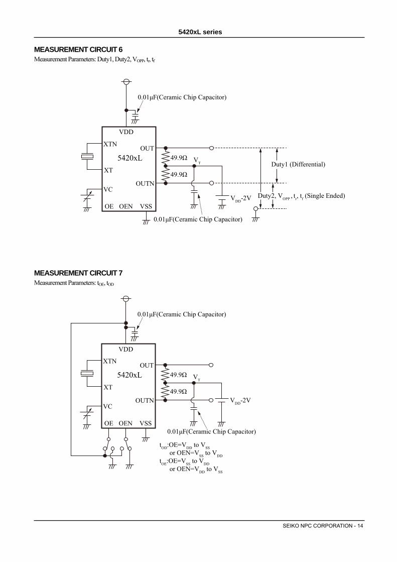
MEASUREMENT CIRCUIT 6 Measurement Parameters: Duty1, Duty2, VOPP, tr, tf MEASUREMENT CIRCUIT 7 Measurement Parameters: tOE, tOD
VDD
XTN
OE VSSOEN
OUTN
XT
5420xL
0.01μF(Ceramic Chip Capacitor)
49.9Ω
49.9Ω
0.01μF(Ceramic Chip Capacitor)
VC
OUT
VT
VDD-2V Duty2, VOPP , tr, tf (Single Ended)
Duty1 (Differential)
VDD
XTN
OE VSSOEN
OUTN
XT
5420xL
0.01μF(Ceramic Chip Capacitor)
49.9Ω
49.9Ω
0.01μF(Ceramic Chip Capacitor)
VC
OUT
VT
VDD-2V
tOD:OE=VDD to VSS or OEN=VSS to VDDtOE:OE=VSS to VDD or OEN=VDD to VSS
5420xL series
SEIKO NPC CORPORATION - 15
MEASUREMENT CIRCUIT 8 Measurement Parameters: FM
VDD
XTN
OE VSSOEN
OUTN
XT
5420xL
0.01μF(Ceramic Chip Capacitor)
49.9Ω
49.9Ω
0.01μF(Ceramic Chip Capacitor)
VC
OUT
VT
SignalGenerator
(AFG3102)
Signal SourceAnalyzer(E5052A)
VC input signal:sine wave, VSS to VDD
0.01μF
EXT Trigger In
50Ω
VDD=2.0V
0.01μF
VSS=-1.3V
5420xL series
SEIKO NPC CORPORATION - 16
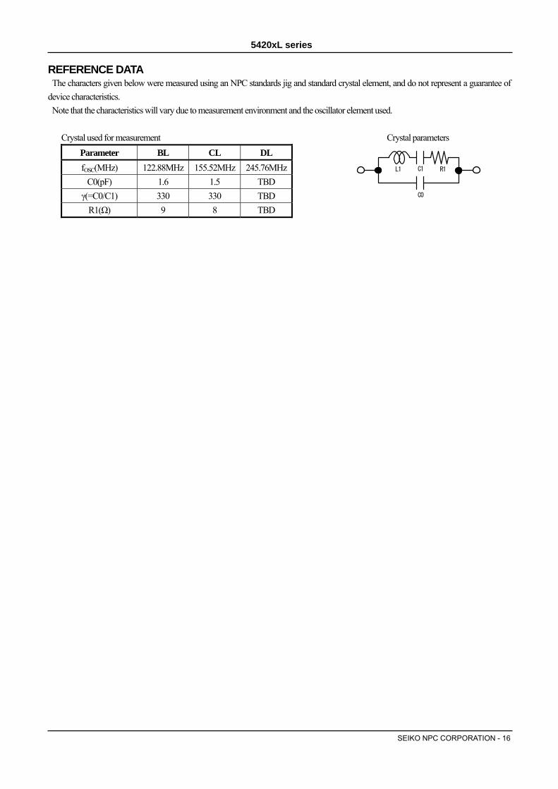
REFERENCE DATA The characters given below were measured using an NPC standards jig and standard crystal element, and do not represent a guarantee of
device characteristics. Note that the characteristics will vary due to measurement environment and the oscillator element used.
Crystal used for measurement Crystal parameters
Parameter BL CL DL fOSC(MHz) 122.88MHz 155.52MHz 245.76MHz
C0(pF) 1.6 1.5 TBD γ(=C0/C1) 330 330 TBD
R1(Ω) 9 8 TBD
C0
L1 C1 R1
5420xL series
SEIKO NPC CORPORATION - 17
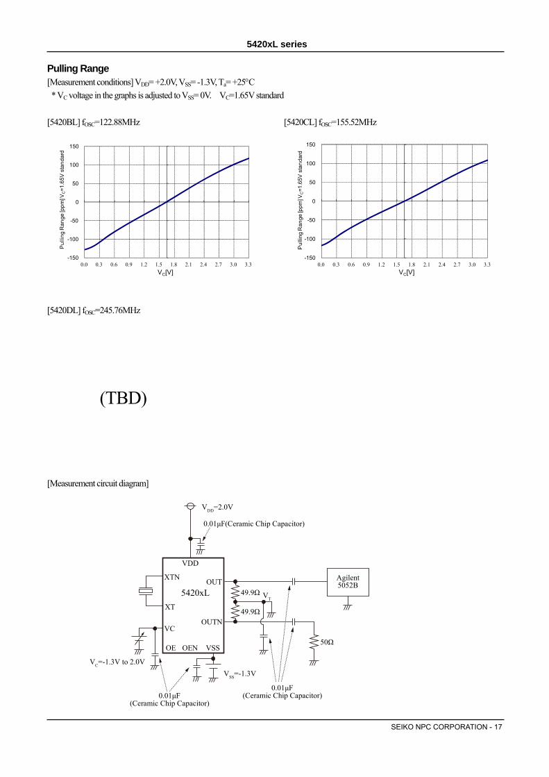
Pulling Range [Measurement conditions] VDD= +2.0V, VSS= -1.3V, Ta= +25°C * VC voltage in the graphs is adjusted to VSS= 0V. VC=1.65V standard
[5420BL] fOSC=122.88MHz [5420CL] fOSC=155.52MHz [5420DL] fOSC=245.76MHz
(TBD) [Measurement circuit diagram]
-150
-100
-50
0
50
100
150
0.0 0.3 0.6 0.9 1.2 1.5 1.8 2.1 2.4 2.7 3.0 3.3
Pul
ling
Ran
ge [p
pm] V
C=1
.65V
sta
ndar
d
VC[V]
-150
-100
-50
0
50
100
150
0.0 0.3 0.6 0.9 1.2 1.5 1.8 2.1 2.4 2.7 3.0 3.3
Pul
ling
Ran
ge [p
pm] V
C=1
.65V
sta
ndar
d
VC[V]
VDD
XTN
OE VSSOEN
OUTN
XT
5420xL
0.01μF(Ceramic Chip Capacitor)
49.9Ω
49.9Ω
0.01μF(Ceramic Chip Capacitor)
VC
OUT
VT
Agilent5052B
50Ω
VDD=2.0V
VSS=-1.3VVC=-1.3V to 2.0V
0.01μF(Ceramic Chip Capacitor)
5420xL series
SEIKO NPC CORPORATION - 18
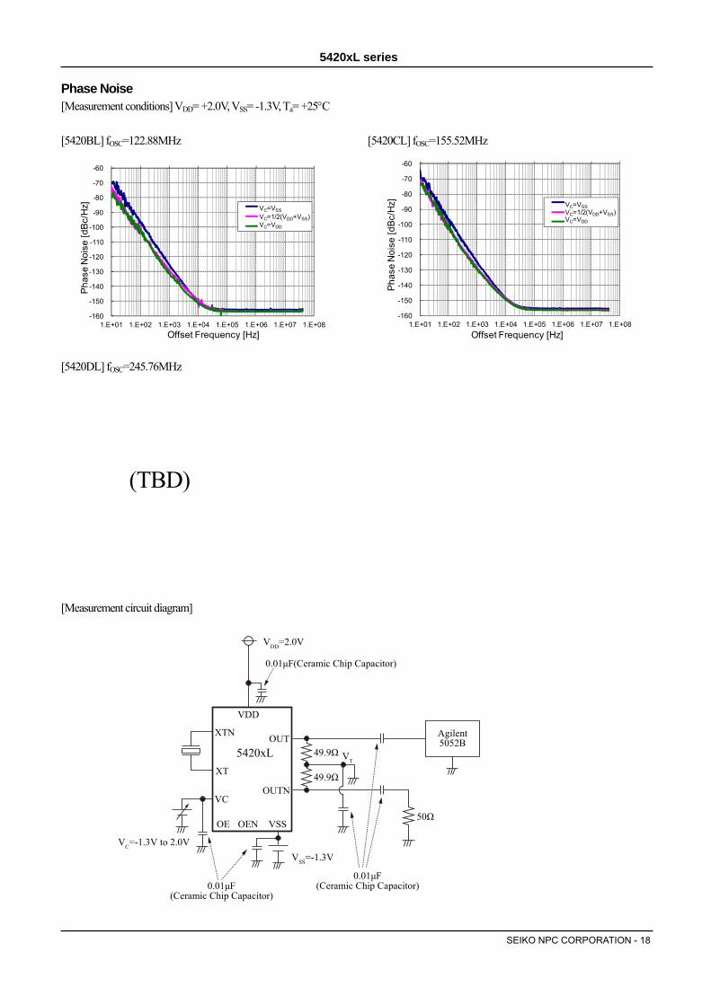
Phase Noise [Measurement conditions] VDD= +2.0V, VSS= -1.3V, Ta= +25°C [5420BL] fOSC=122.88MHz [5420CL] fOSC=155.52MHz [5420DL] fOSC=245.76MHz
(TBD) [Measurement circuit diagram]
-160
-150
-140
-130
-120
-110
-100
-90
-80
-70
-60
1.E+01 1.E+02 1.E+03 1.E+04 1.E+05 1.E+06 1.E+07 1.E+08
Pha
se N
oise
[dBc
/Hz]
Offset Frequency [Hz]
VC=VSS
VC=1/2(VDD+VSS)
VC=VDD
VC=VSSVC=1/2(VDD+VSS)VC=VDD
-160
-150
-140
-130
-120
-110
-100
-90
-80
-70
-60
1.E+01 1.E+02 1.E+03 1.E+04 1.E+05 1.E+06 1.E+07 1.E+08
Phas
e N
oise
[dBc
/Hz]
Offset Frequency [Hz]
VC=VSS
VC=1/2(VDD+VSS)
VC=VDD
VC=VSSVC=1/2(VDD+VSS)VC=VDD
VDD
XTN
OE VSSOEN
OUTN
XT
5420xL
0.01μF(Ceramic Chip Capacitor)
49.9Ω
49.9Ω
0.01μF(Ceramic Chip Capacitor)
VC
OUT
VT
Agilent5052B
50Ω
VDD=2.0V
VSS=-1.3VVC=-1.3V to 2.0V
0.01μF(Ceramic Chip Capacitor)
5420xL series
SEIKO NPC CORPORATION - 19
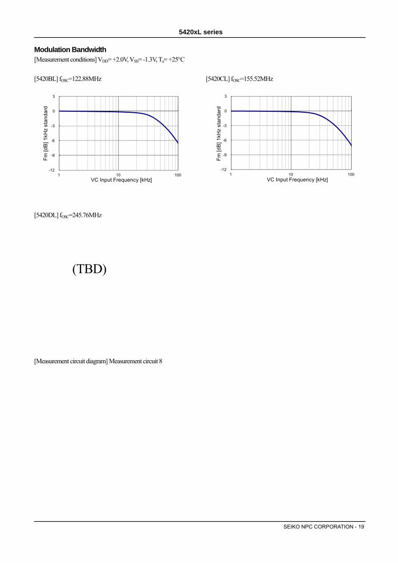
Modulation Bandwidth [Measurement conditions] VDD= +2.0V, VSS= -1.3V, Ta= +25°C [5420BL] fOSC=122.88MHz [5420CL] fOSC=155.52MHz [5420DL] fOSC=245.76MHz
(TBD) [Measurement circuit diagram] Measurement circuit 8
-12
-9
-6
-3
0
3
1 10 100
Fm [d
B] 1
kHz
stan
dard
VC Input Frequency [kHz]
-12
-9
-6
-3
0
3
1 10 100
Fm [d
B] 1
kHz
stan
dard
VC Input Frequency [kHz]
5420xL series
SEIKO NPC CORPORATION - 20
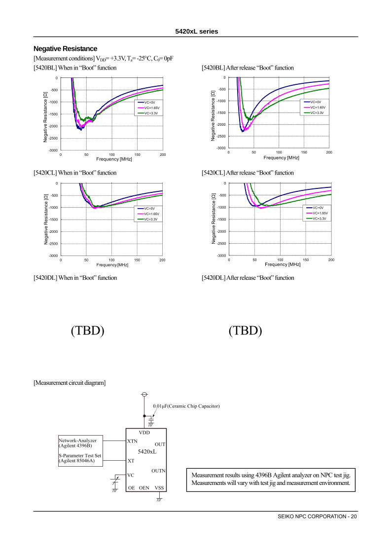
Negative Resistance [Measurement conditions] VDD= +3.3V, Ta= -25°C, C0= 0pF [5420BL] When in “Boot” function [5420BL] After release “Boot” function [5420CL] When in “Boot” function [5420CL] After release “Boot” function [5420DL] When in “Boot” function [5420DL] After release “Boot” function
(TBD) (TBD) [Measurement circuit diagram]
Measurement results using 4396B Agilent analyzer on NPC test jig. Measurements will vary with test jig and measurement environment.
-3000
-2500
-2000
-1500
-1000
-500
0
0 50 100 150 200
Neg
ativ
e R
esis
tanc
e [Ω
]
Frequency [MHz]
VC=0VVC=1.65VVC=3.3V
-3000
-2500
-2000
-1500
-1000
-500
0
0 50 100 150 200
Neg
ativ
e R
esis
tanc
e [Ω
]
Frequency [MHz]
VC=0VVC=1.65VVC=3.3V
-3000
-2500
-2000
-1500
-1000
-500
0
0 50 100 150 200
Neg
ativ
e R
esis
tanc
e [Ω
]
Frequency [MHz]
VC=0VVC=1.65VVC=3.3V
-3000
-2500
-2000
-1500
-1000
-500
0
0 50 100 150 200
Neg
ativ
e R
esis
tanc
e [Ω
]
Frequency [MHz]
VC=0VVC=1.65VVC=3.3V
VDD
XTN
OE VSSOEN
OUTN
XT
5420xL
0.01μF(Ceramic Chip Capacitor)
VC
OUTNetwork-Analyzer(Agilent 4396B)
S-Parameter Test Set(Agilent 85046A)
5420xL series
SEIKO NPC CORPORATION - 21
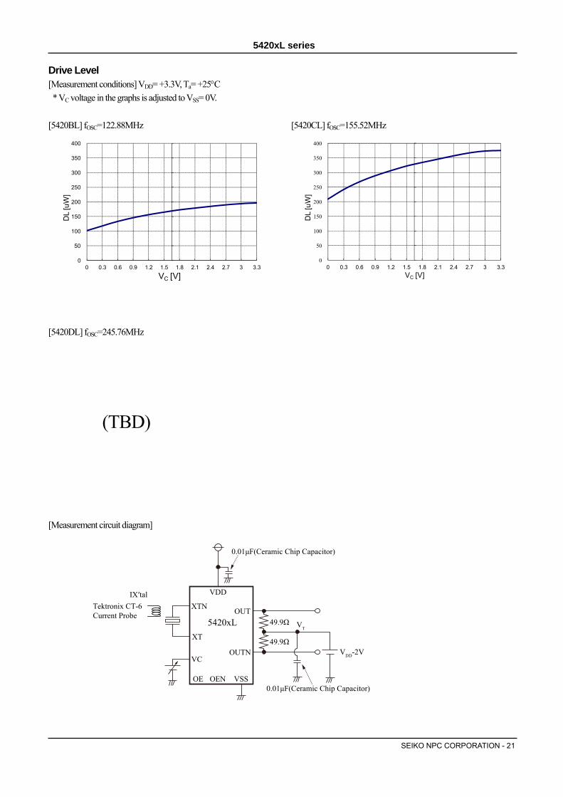
Drive Level [Measurement conditions] VDD= +3.3V, Ta= +25°C * VC voltage in the graphs is adjusted to VSS= 0V.
[5420BL] fOSC=122.88MHz [5420CL] fOSC=155.52MHz [5420DL] fOSC=245.76MHz
(TBD) [Measurement circuit diagram]
0
50
100
150
200
250
300
350
400
0 0.3 0.6 0.9 1.2 1.5 1.8 2.1 2.4 2.7 3 3.3
DL
[uW
]
VC [V]
0
50
100
150
200
250
300
350
400
0 0.3 0.6 0.9 1.2 1.5 1.8 2.1 2.4 2.7 3 3.3
DL
[uW
]
VC [V]
VDD
XTN
OE VSSOEN
OUTN
XT
5420xL
0.01μF(Ceramic Chip Capacitor)
49.9Ω
49.9Ω
0.01μF(Ceramic Chip Capacitor)
VC
OUT
VT
VDD-2V
Tektronix CT-6Current Probe
IX′tal
5420xL series
SEIKO NPC CORPORATION - 22
CLOSC: Oscillator circuit equivalent capacitance determined by oscillator frequency
021
1C
fsf
CCLoscOSC
−
−⎟⎟⎠
⎞⎜⎜⎝
⎛=
C1: Crystal element equivalent series capacitance C0: Crystal element equivalent parallel capacitance fs: Crystal element series resonance frequency
Oscillator CL Characteristics [Measurement conditions] VDD= +2.0V, VSS= -1.3V, Ta= +25°C * VC voltage in the graphs is adjusted to VSS= 0V.
[5420BL] fOSC=122.88MHz [5420CL] fOSC=155.52MHz [5420DL] fOSC=245.76MHz
(TBD) [Measurement circuit diagram]
0.0
0.5
1.0
1.5
2.0
2.5
3.0
3.5
4.0
4.5
5.0
0.0 0.3 0.6 0.9 1.2 1.5 1.8 2.1 2.4 2.7 3.0 3.3
CL O
SC[p
F]
VC [V]
0.0
0.5
1.0
1.5
2.0
2.5
3.0
3.5
4.0
4.5
5.0
0.0 0.3 0.6 0.9 1.2 1.5 1.8 2.1 2.4 2.7 3.0 3.3
CL O
SC[p
F]
VC [V]
VDD
XTN
OE VSSOEN
OUTN
XT
5420xL
0.01μF(Ceramic Chip Capacitor)
49.9Ω
49.9Ω
0.01μF(Ceramic Chip Capacitor)
VC
OUT
VT
Agilent5052B
50Ω
VDD=2.0V
VSS=-1.3VVC=-1.3V to 2.0V
0.01μF(Ceramic Chip Capacitor)
5420xL series
SEIKO NPC CORPORATION - 23
VC Terminal Input Impedance [Measurement conditions] Ta= +25°C, VC= 0V [5420BL, CL] [5420DL]
(TBD) [Measurement circuit diagram]
0
100
200
300
400
500
600
0 10 20 30 40 50 60 70 80 90 100
VC In
put I
mpe
danc
e [kΩ
]
VC Input Frequency [kHz]
VDDXTN
OE VSSOEN
OUTN
XT
5420xL
VC
OUT
ImpedanceAnalyzer
(HP 4194A)
VC input signal: 1kHz to 100kHz, 0.1VP-P
5420xL series
SEIKO NPC CORPORATION - 24
Output Waveform [Measurement conditions] VDD= +3.3V, VC= +1.65V, Ta= +25°C [5420BL] fOSC=122.88MHz [5420CL] fOSC=155.52MHz [5420DL] fOSC=245.76MHz
(TBD) [Measurement circuit diagram] Measurement circuit 6
Measurement equipment: Oscilloscope DSO80604B (Agilent), Differential probe 1134A (Probe head E2678A)
OUTN
OUT
diff
OUTN
OUT
diff
5420xL series
SEIKO NPC CORPORATION - 25
Output Enable Propagation Delay [Measurement conditions] VDD= +3.3V, VC= +1.65V, Ta= +25°C [5420BL] fOSC=122.88MHz [5420CL] fOSC=155.52MHz [5420DL] fOSC=245.76MHz
(TBD)
* tOE is the time required for the output level to stabilize, and which varies depending on the power supply used, bypass capacitor values, and other factors.
Measurement equipment: Power supply voltage PW18-1.8AQYB (KENWOOD) [Measurement circuit diagram]
OUTN
OUT
OE
VDD
XTN
OE VSSOEN
OUTN
XT
5420xL
0.01μF(Ceramic Chip Capacitor)
49.9Ω
49.9Ω
0.01μF(Ceramic Chip Capacitor)
VC
OUT
VT
VDD-2V
Oscilloscope(Agilent DSO80304B)
TektronixAFG3012
49.9Ω
OUTN
OUT
OE
5420xL series
SEIKO NPC CORPORATION - 26
Please pay your attention to the following points at time of using the products shown in this document. 1. The products shown in this document (hereinafter ”Products”) are designed and manufactured to the generally accepted standards of
reliability as expected for use in general electronic and electrical equipment, such as personal equipment, machine tools and measurement equipment. The Products are not designed and manufactured to be used in any other special equipment requiring extremely high level of reliability and safety, such as aerospace equipment, nuclear power control equipment, medical equipment, transportation equipment, disaster prevention equipment, security equipment. The Products are not designed and manufactured to be used for the apparatus that exerts harmful influence on the human lives due to the defects, failure or malfunction of the Products.
If you wish to use the Products in that apparatus, please contact our sales section in advance. In the event that the Products are used in such apparatus without our prior approval, we assume no responsibility whatsoever for any
damages resulting from the use of that apparatus. 2. NPC reserves the right to change the specifications of the Products in order to improve the characteristics or reliability thereof. 3. The information described in this document is presented only as a guide for using the Products. No responsibility is assumed by us for any
infringements of patents or other rights of the third parties which may result from its use. No license is granted by implication or otherwise under any patents or other rights of the third parties. Then, we assume no responsibility whatsoever for any damages resulting from that infringements.
4. The constant of each circuit shown in this document is described as an example, and it is not guaranteed about its value of the mass production products.
5. In the case of that the Products in this document falls under the foreign exchange and foreign trade control law or other applicable laws and regulations, approval of the export to be based on those laws and regulations are necessary. Customers are requested appropriately take steps to obtain required permissions or approvals from appropriate government agencies.
SEIKO NPC CORPORATION 1-9-9, Hatchobori, Chuo-ku, Tokyo 104-0032, Japan Telephone: +81-3-5541-6501 Facsimile: +81-3-5541-6510 http://www.npc.co.jp/ Email:[email protected] ND14006-E-00 2014.06