50 nominal input / conjugate match balun to SPIRIT1, with ... › content › ccc › resource ›...
12
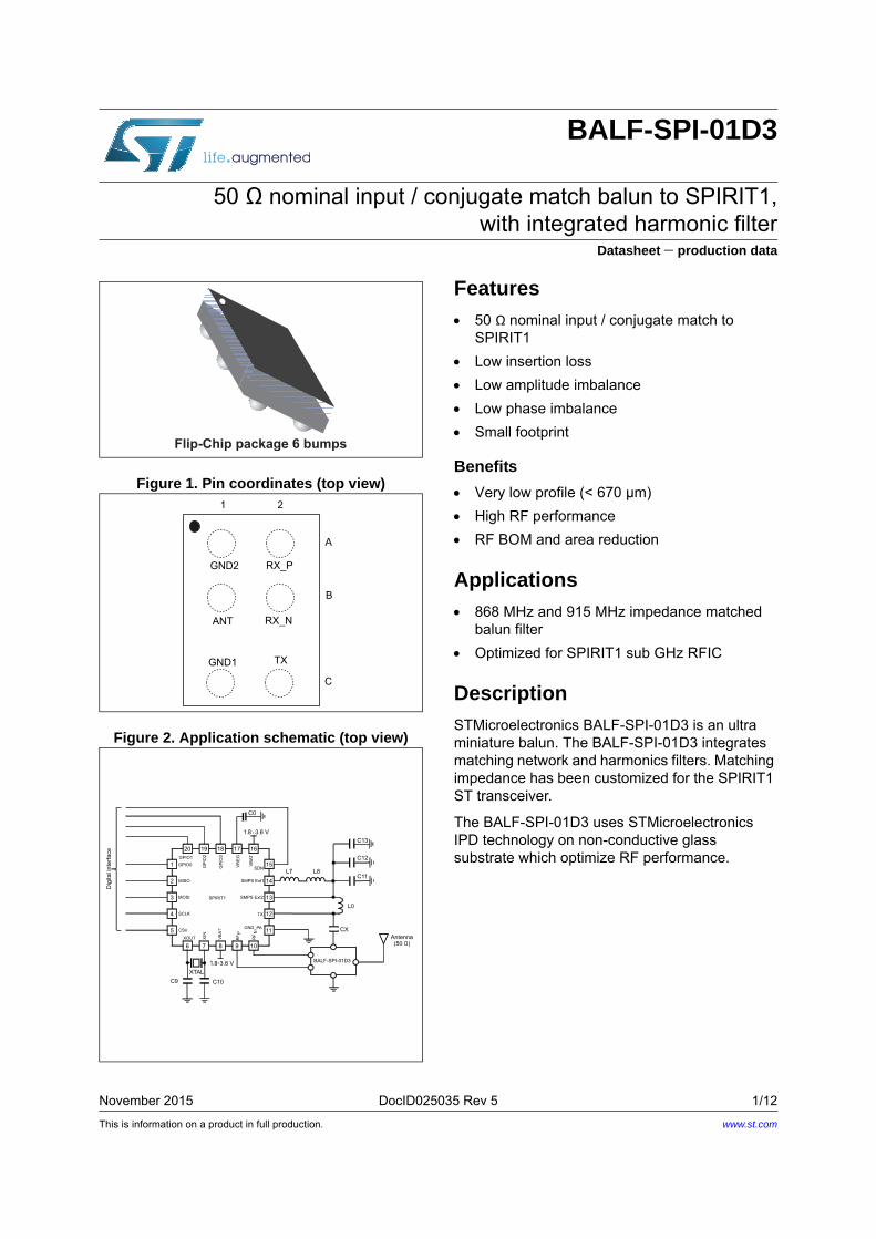
This is information on a product in full production. November 2015 DocID025035 Rev 5 1/12 12 BALF-SPI-01D3 50 Ω nominal input / conjugate match balun to SPIRIT1, with integrated harmonic filter Datasheet production data Figure 1. Pin coordinates (top view) Figure 2. Application schematic (top view) Features 50 Ω nominal input / conjugate match to SPIRIT1 Low insertion loss Low amplitude imbalance Low phase imbalance Small footprint Benefits Very low profile (< 670 μm) High RF performance RF BOM and area reduction Applications 868 MHz and 915 MHz impedance matched balun filter Optimized for SPIRIT1 sub GHz RFIC Description STMicroelectronics BALF-SPI-01D3 is an ultra miniature balun. The BALF-SPI-01D3 integrates matching network and harmonics filters. Matching impedance has been customized for the SPIRIT1 ST transceiver. The BALF-SPI-01D3 uses STMicroelectronics IPD technology on non-conductive glass substrate which optimize RF performance. Flip-Chip package 6 bumps www.st.com
Transcript of 50 nominal input / conjugate match balun to SPIRIT1, with ... › content › ccc › resource ›...
This is information on a product in full production.
November 2015 DocID025035 Rev 5 1/12
12
BALF-SPI-01D3
50 Ω nominal input / conjugate match balun to SPIRIT1,with integrated harmonic filter
Datasheet production data
Figure 1. Pin coordinates (top view)
Figure 2. Application schematic (top view)
Features
50 Ω nominal input / conjugate match to SPIRIT1
Low insertion loss
Low amplitude imbalance
Low phase imbalance
Small footprint
Benefits
Very low profile (< 670 μm)
High RF performance
RF BOM and area reduction
Applications
868 MHz and 915 MHz impedance matched balun filter
Optimized for SPIRIT1 sub GHz RFIC
Description
STMicroelectronics BALF-SPI-01D3 is an ultra miniature balun. The BALF-SPI-01D3 integrates matching network and harmonics filters. Matching impedance has been customized for the SPIRIT1 ST transceiver.
The BALF-SPI-01D3 uses STMicroelectronics IPD technology on non-conductive glass substrate which optimize RF performance.
Flip-Chip package 6 bumps
www.st.com
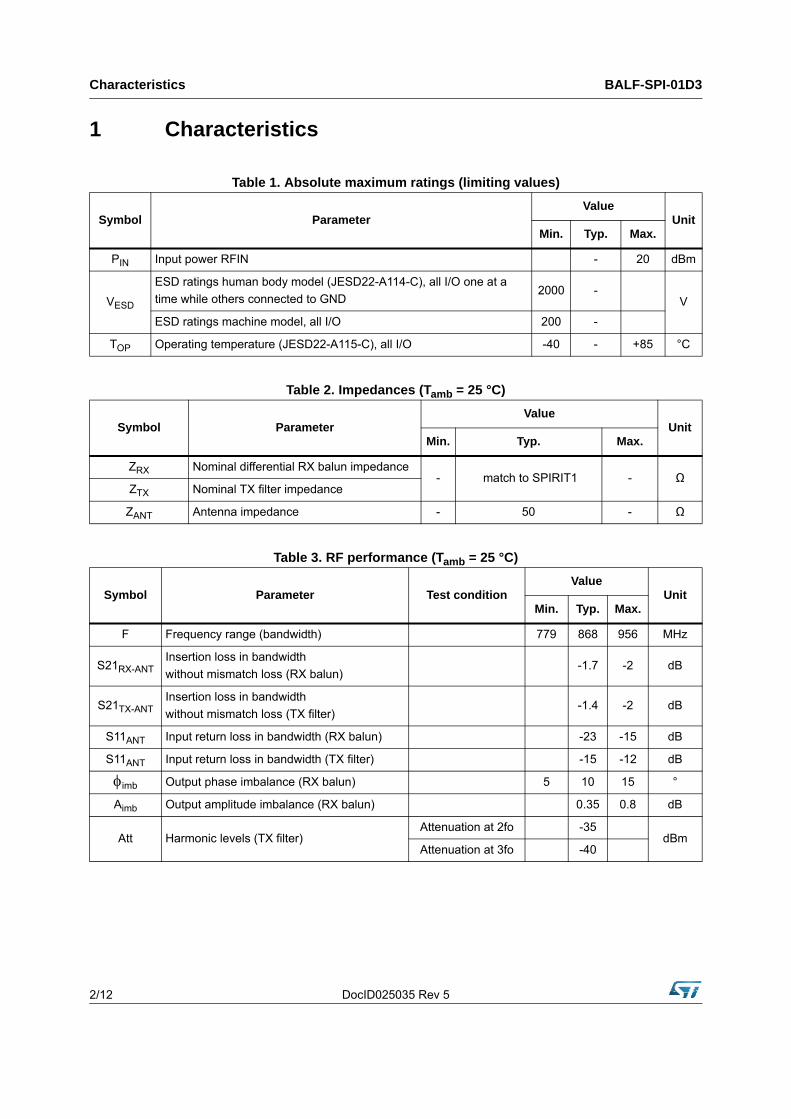
Characteristics BALF-SPI-01D3
2/12 DocID025035 Rev 5
1 Characteristics
Table 1. Absolute maximum ratings (limiting values)
Symbol ParameterValue
UnitMin. Typ. Max.
PIN Input power RFIN - 20 dBm
VESD
ESD ratings human body model (JESD22-A114-C), all I/O one at a
time while others connected to GND2000 -
V
ESD ratings machine model, all I/O 200 -
TOP Operating temperature (JESD22-A115-C), all I/O -40 - +85 °C
Table 2. Impedances (Tamb = 25 °C)
Symbol ParameterValue
UnitMin. Typ. Max.
ZRX Nominal differential RX balun impedance- match to SPIRIT1 - Ω
ZTX Nominal TX filter impedance
ZANT Antenna impedance - 50 - Ω
Table 3. RF performance (Tamb = 25 °C)
Symbol Parameter Test conditionValue
UnitMin. Typ. Max.
F Frequency range (bandwidth) 779 868 956 MHz
S21RX-ANTInsertion loss in bandwidth
without mismatch loss (RX balun)-1.7 -2 dB
S21TX-ANTInsertion loss in bandwidth
without mismatch loss (TX filter)-1.4 -2 dB
S11ANT Input return loss in bandwidth (RX balun) -23 -15 dB
S11ANT Input return loss in bandwidth (TX filter) -15 -12 dB
imb Output phase imbalance (RX balun) 5 10 15 °
Aimb Output amplitude imbalance (RX balun) 0.35 0.8 dB
Att Harmonic levels (TX filter)Attenuation at 2fo -35
dBmAttenuation at 3fo -40
DocID025035 Rev 5 3/12
BALF-SPI-01D3 Characteristics
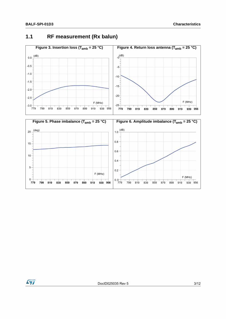
1.1 RF measurement (Rx balun)
Figure 3. Insertion loss (Tamb = 25 °C) Figure 4. Return loss antenna (Tamb = 25 °C)
Figure 5. Phase imbalance (Tamb = 25 °C) Figure 6. Amplitude imbalance (Tamb = 25 °C)
Characteristics BALF-SPI-01D3
4/12 DocID025035 Rev 5
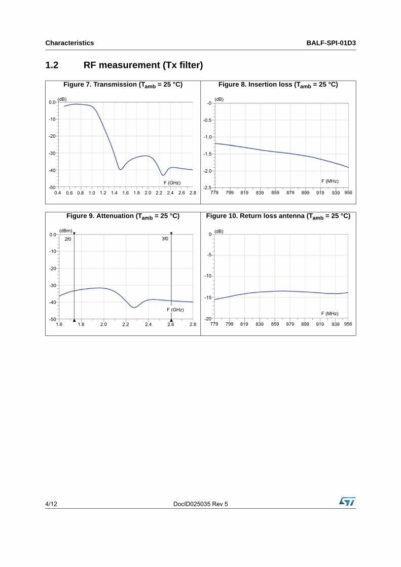
1.2 RF measurement (Tx filter)
Figure 7. Transmission (Tamb = 25 °C) Figure 8. Insertion loss (Tamb = 25 °C)
Figure 9. Attenuation (Tamb = 25 °C) Figure 10. Return loss antenna (Tamb = 25 °C)
DocID025035 Rev 5 5/12
BALF-SPI-01D3 Application information
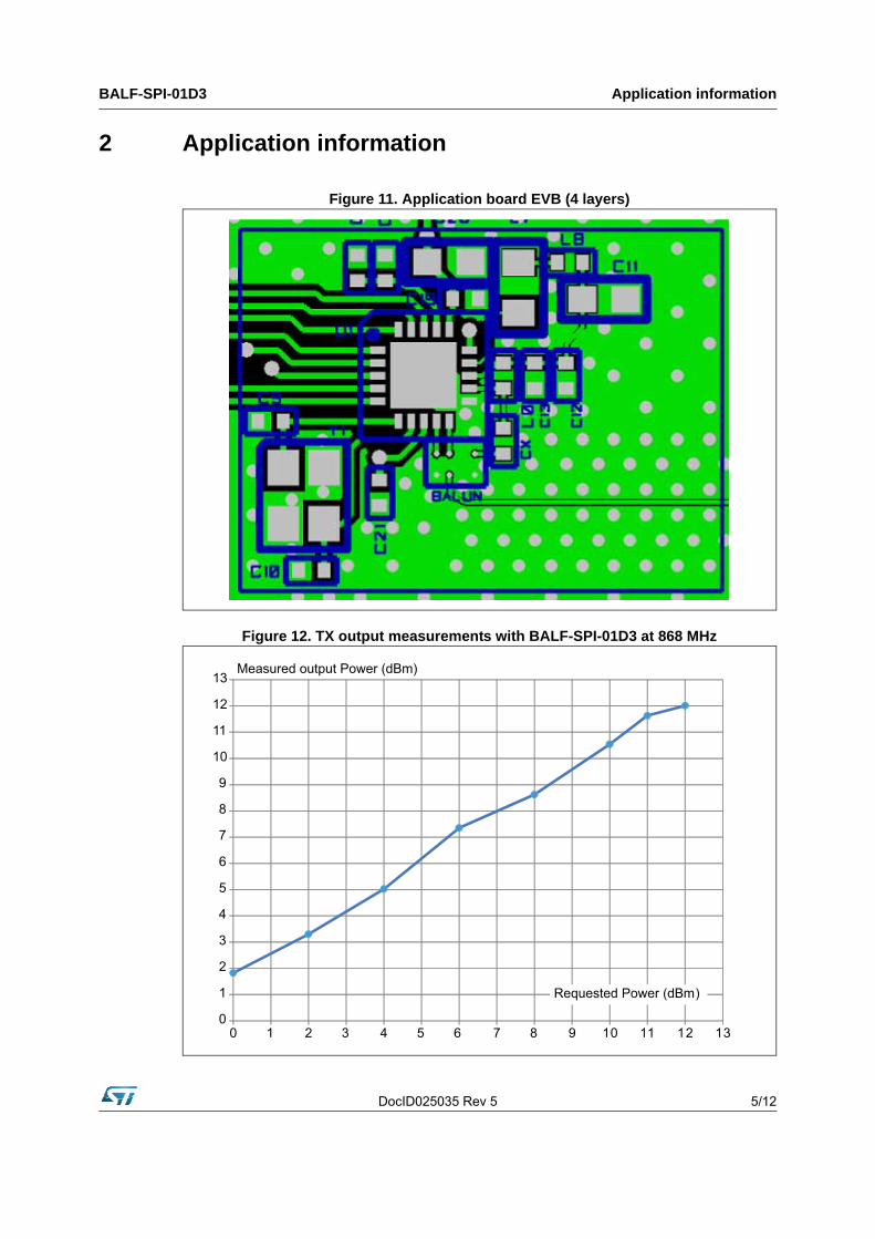
2 Application information
Figure 11. Application board EVB (4 layers)
Figure 12. TX output measurements with BALF-SPI-01D3 at 868 MHz
Application information BALF-SPI-01D3
6/12 DocID025035 Rev 5
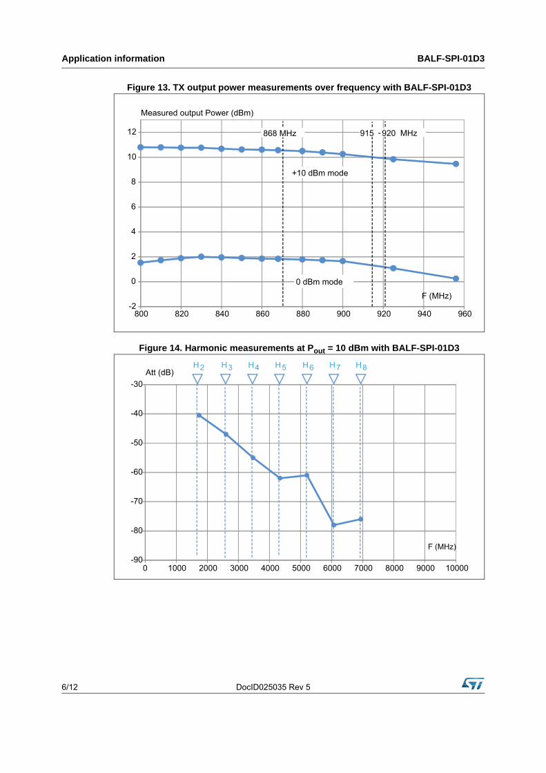
Figure 13. TX output power measurements over frequency with BALF-SPI-01D3
Figure 14. Harmonic measurements at Pout = 10 dBm with BALF-SPI-01D3
DocID025035 Rev 5 7/12
BALF-SPI-01D3 Package information
3 Package information
Epoxy meets UL94, V0
Lead-free package
In order to meet environmental requirements, ST offers these devices in different grades of ECOPACK® packages, depending on their level of environmental compliance. ECOPACK® specifications, grade definitions and product status are available at: www.st.com. ECOPACK® is an ST trademark.
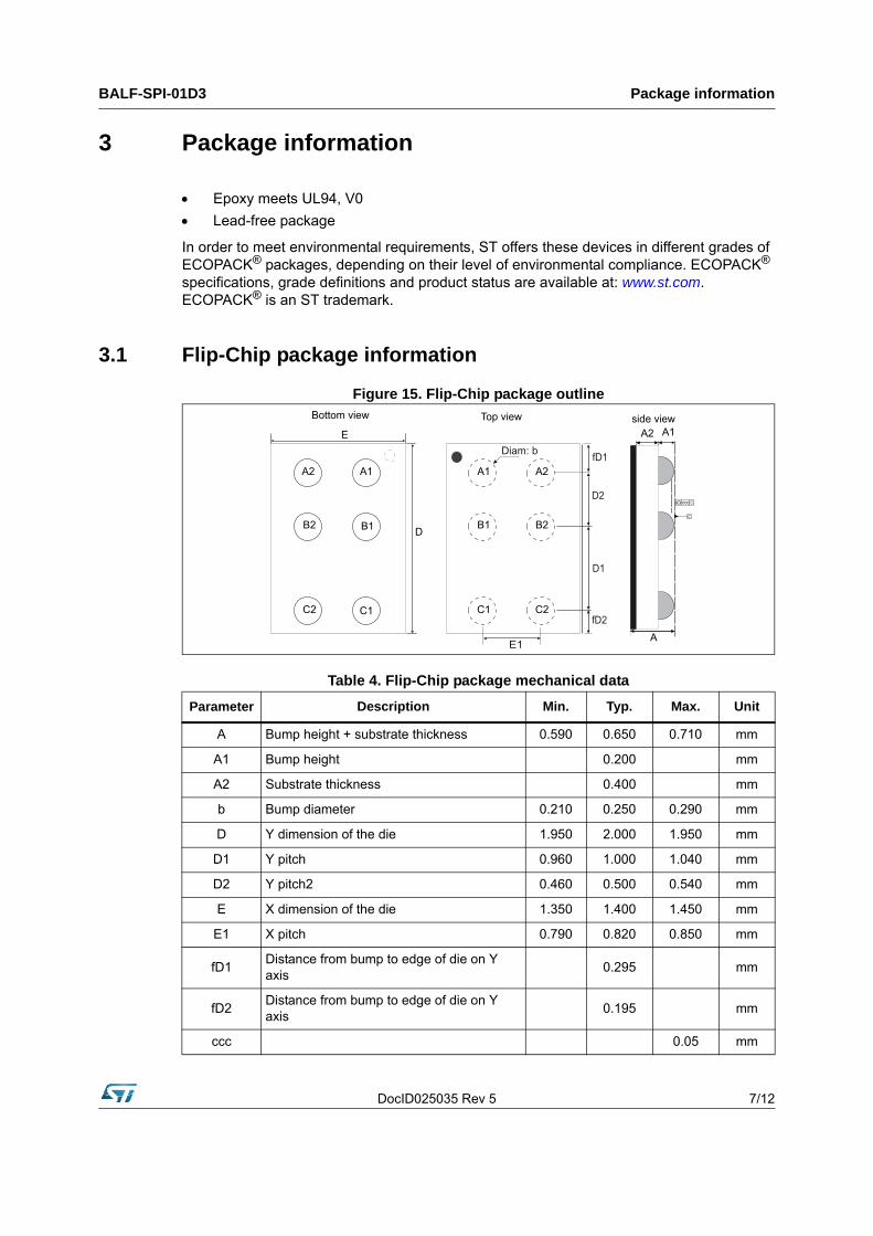
3.1 Flip-Chip package information
Figure 15. Flip-Chip package outline
Table 4. Flip-Chip package mechanical data
Parameter Description Min. Typ. Max. Unit
A Bump height + substrate thickness 0.590 0.650 0.710 mm
A1 Bump height 0.200 mm
A2 Substrate thickness 0.400 mm
b Bump diameter 0.210 0.250 0.290 mm
D Y dimension of the die 1.950 2.000 1.950 mm
D1 Y pitch 0.960 1.000 1.040 mm
D2 Y pitch2 0.460 0.500 0.540 mm
E X dimension of the die 1.350 1.400 1.450 mm
E1 X pitch 0.790 0.820 0.850 mm
fD1Distance from bump to edge of die on Y axis
0.295 mm
fD2Distance from bump to edge of die on Y axis
0.195 mm
ccc 0.05 mm
Package information BALF-SPI-01D3
8/12 DocID025035 Rev 5
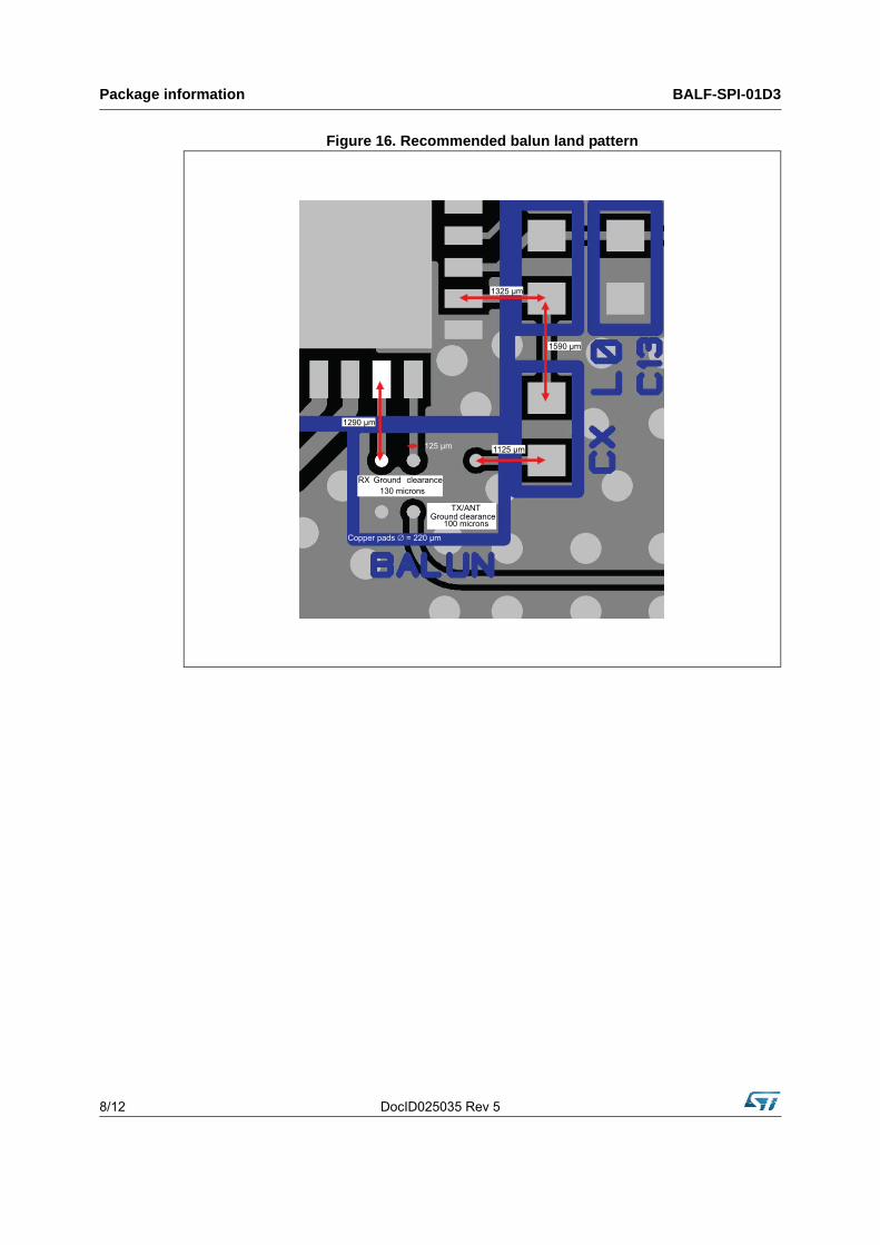
Figure 16. Recommended balun land pattern
DocID025035 Rev 5 9/12
BALF-SPI-01D3 Package information
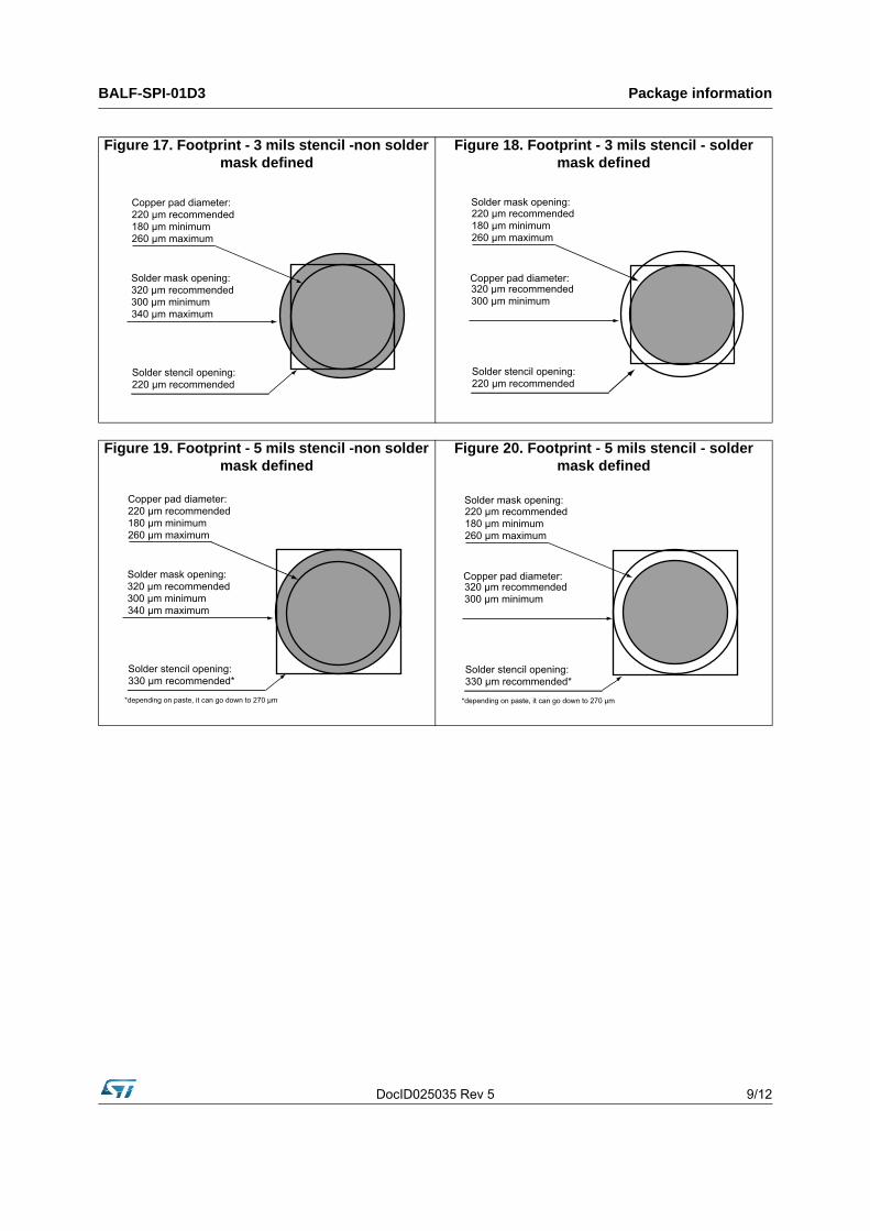
Figure 17. Footprint - 3 mils stencil -non solder mask defined
Figure 18. Footprint - 3 mils stencil - solder mask defined
Figure 19. Footprint - 5 mils stencil -non solder mask defined
Figure 20. Footprint - 5 mils stencil - solder mask defined
Package information BALF-SPI-01D3
10/12 DocID025035 Rev 5
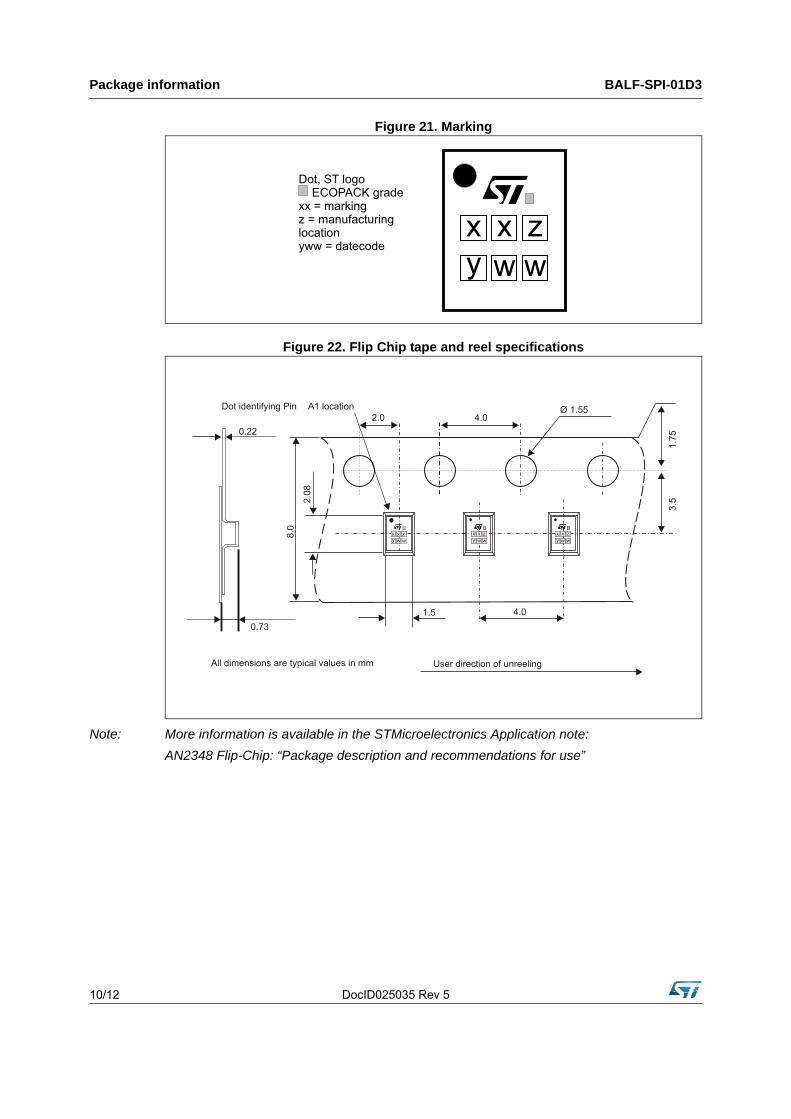
Figure 21. Marking
Figure 22. Flip Chip tape and reel specifications
Note: More information is available in the STMicroelectronics Application note:
AN2348 Flip-Chip: “Package description and recommendations for use”
DocID025035 Rev 5 11/12
BALF-SPI-01D3 Ordering information
4 Ordering information
5 Revision history
Table 5. Ordering information
Order code Marking Weight Base Qty Delivery mode
BALF-SPI-01D3 SJ 3.0 mg 5000 Tape and Reel
Table 6. Document revision history
Date Revision Changes
27-Aug-2013 1 Initial release.
03-Oct-2013 2 Updated document title. Updated Table 1 with JESD22 references.
15-May-2015 3 Updated Figure 1 and Figure 15. Added Figure 19 and Figure 20.
18-Sep-2015 4 Updated Figure 15 and added Table 4.
17-Nov-2015 5 Updated Figure 2 and Figure 15.
BALF-SPI-01D3
12/12 DocID025035 Rev 5
IMPORTANT NOTICE – PLEASE READ CAREFULLY
STMicroelectronics NV and its subsidiaries (“ST”) reserve the right to make changes, corrections, enhancements, modifications, and improvements to ST products and/or to this document at any time without notice. Purchasers should obtain the latest relevant information on ST products before placing orders. ST products are sold pursuant to ST’s terms and conditions of sale in place at the time of order acknowledgement.
Purchasers are solely responsible for the choice, selection, and use of ST products and ST assumes no liability for application assistance or the design of Purchasers’ products.
No license, express or implied, to any intellectual property right is granted by ST herein.
Resale of ST products with provisions different from the information set forth herein shall void any warranty granted by ST for such product.
ST and the ST logo are trademarks of ST. All other product or service names are the property of their respective owners.
Information in this document supersedes and replaces information previously supplied in any prior versions of this document.
© 2015 STMicroelectronics – All rights reserved