
3 Detector Structures
51
M. Krammer, XI ICFA School on Instrumentation Silicon Detectors 1 3 Detector Structures
Transcript of 3 Detector Structures
M. Krammer, XI ICFA School on Instrumentation Silicon Detectors 1
3 Detector Structures
M. Krammer, XI ICFA School on Instrumentation Silicon Detectors 2
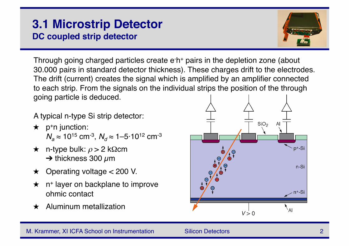
★ p+n junction: Na ≈ 1015 cm-3, Nd ≈ 1–5·1012 cm-3
★ n-type bulk: ρ > 2 kΩcm➔ thickness 300 µm
★ Operating voltage < 200 V. ★ n+ layer on backplane to improve
ohmic contact ★ Aluminum metallization
3.1 Microstrip DetectorDC coupled strip detector
Through going charged particles create e-h+ pairs in the depletion zone (about 30.000 pairs in standard detector thickness). These charges drift to the electrodes. The drift (current) creates the signal which is amplified by an amplifier connected to each strip. From the signals on the individual strips the position of the through going particle is deduced.
A typical n-type Si strip detector:
M. Krammer, XI ICFA School on Instrumentation Silicon Detectors 3
3.1 Microstrip Detectorn-type and p-type detectors
Note:
The previous slide explains an n-type detector (detector bulk is n-type silicon)
Using p-type silicon and exchanging p+ and n+ would give a perfectly working p-type detector.
For tradition and production reasons most detectors used are n-type detectors. p-type detectors have some advantages in high radiation environment (see later).
For simplicity I will continue discussing n-type detectors only...
M. Krammer, XI ICFA School on Instrumentation Silicon Detectors 4
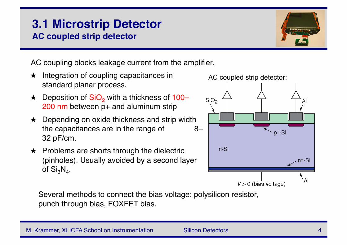
3.1 Microstrip DetectorAC coupled strip detector
★ Integration of coupling capacitances in standard planar process.
★ Deposition of SiO2 with a thickness of 100–200 nm between p+ and aluminum strip
★ Depending on oxide thickness and strip width the capacitances are in the range of 8–32 pF/cm.
★ Problems are shorts through the dielectric (pinholes). Usually avoided by a second layer of Si3N4.
AC coupled strip detector:
Several methods to connect the bias voltage: polysilicon resistor, punch through bias, FOXFET bias.
AC coupling blocks leakage current from the amplifier.
M. Krammer, XI ICFA School on Instrumentation Silicon Detectors 5
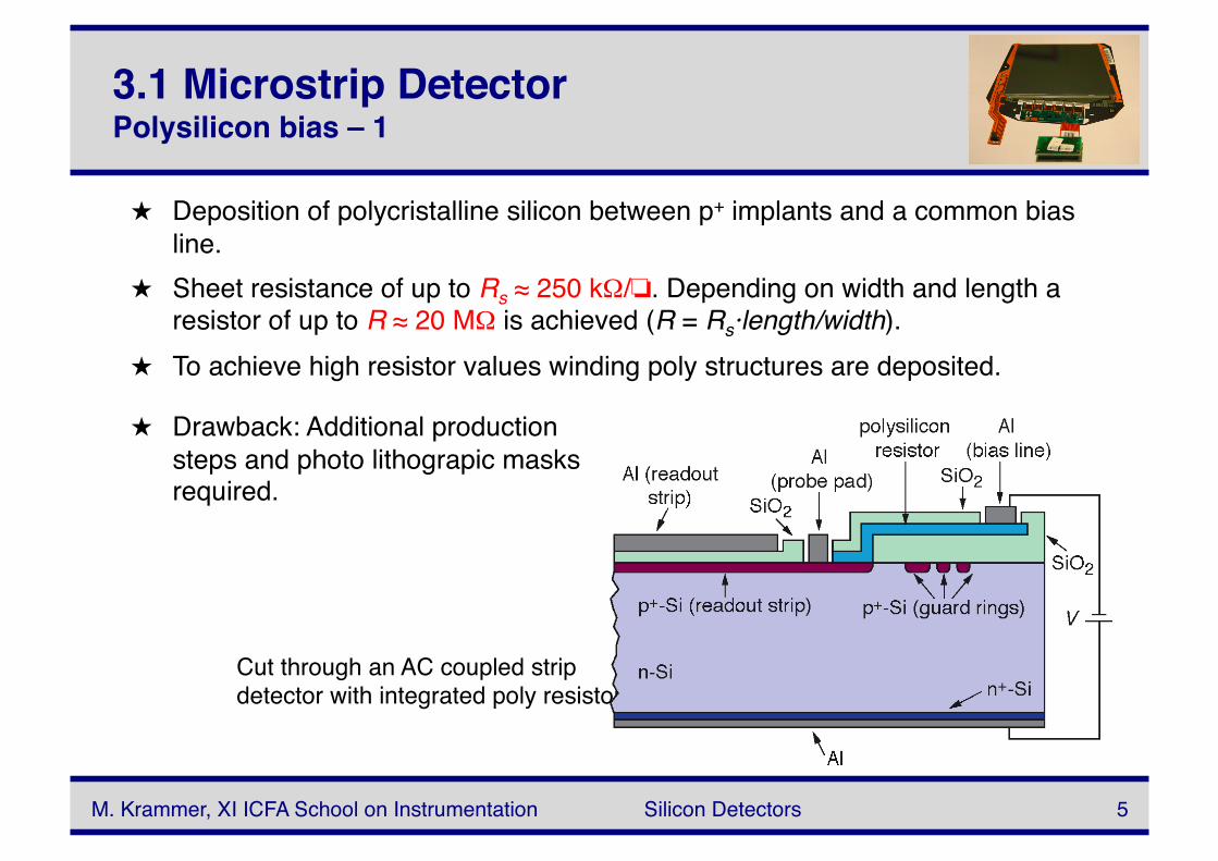
3.1 Microstrip DetectorPolysilicon bias – 1
★ Drawback: Additional production steps and photo lithograpic masks required.
Cut through an AC coupled strip detector with integrated poly resistors:
★ Deposition of polycristalline silicon between p+ implants and a common bias line.
★ Sheet resistance of up to Rs ≈ 250 kΩ/❏. Depending on width and length a resistor of up to R ≈ 20 MΩ is achieved (R = Rs·length/width).
★ To achieve high resistor values winding poly structures are deposited.
M. Krammer, XI ICFA School on Instrumentation Silicon Detectors 6
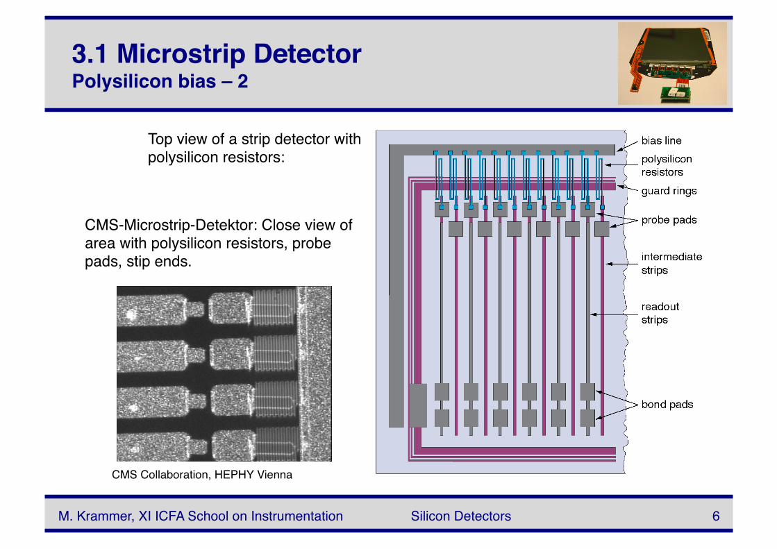
3.1 Microstrip DetectorPolysilicon bias – 2
Top view of a strip detector with polysilicon resistors:
CMS-Microstrip-Detektor: Close view of area with polysilicon resistors, probe pads, stip ends.
CMS Collaboration, HEPHY Vienna
M. Krammer, XI ICFA School on Instrumentation Silicon Detectors 7
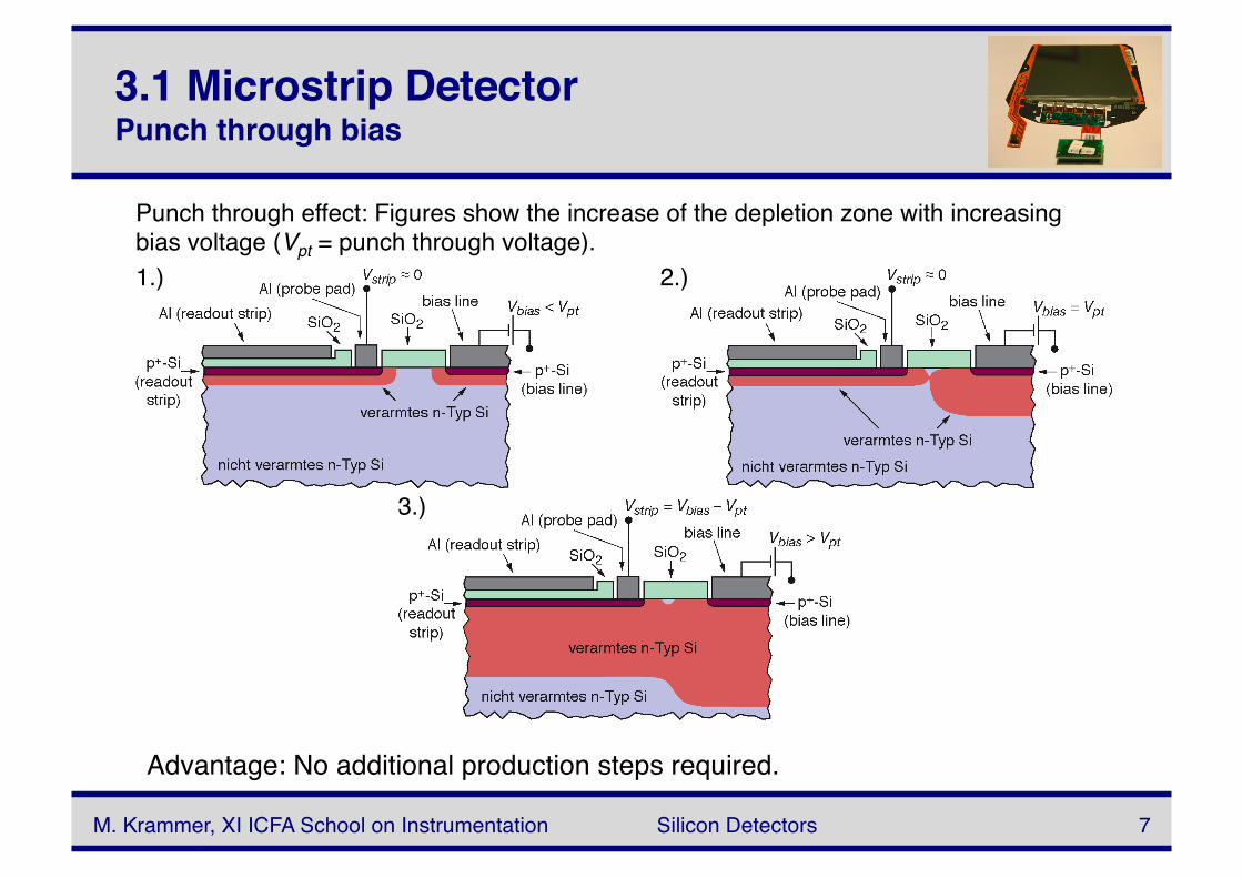
3.1 Microstrip DetectorPunch through bias
Punch through effect: Figures show the increase of the depletion zone with increasing bias voltage (Vpt = punch through voltage).
3.)
1.) 2.)
Advantage: No additional production steps required.
M. Krammer, XI ICFA School on Instrumentation Silicon Detectors 8
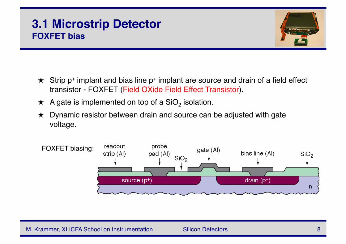
3.1 Microstrip DetectorFOXFET bias
FOXFET biasing:
★ Strip p+ implant and bias line p+ implant are source and drain of a field effect transistor - FOXFET (Field OXide Field Effect Transistor).
★ A gate is implemented on top of a SiO2 isolation. ★ Dynamic resistor between drain and source can be adjusted with gate
voltage.
M. Krammer, XI ICFA School on Instrumentation Silicon Detectors 9
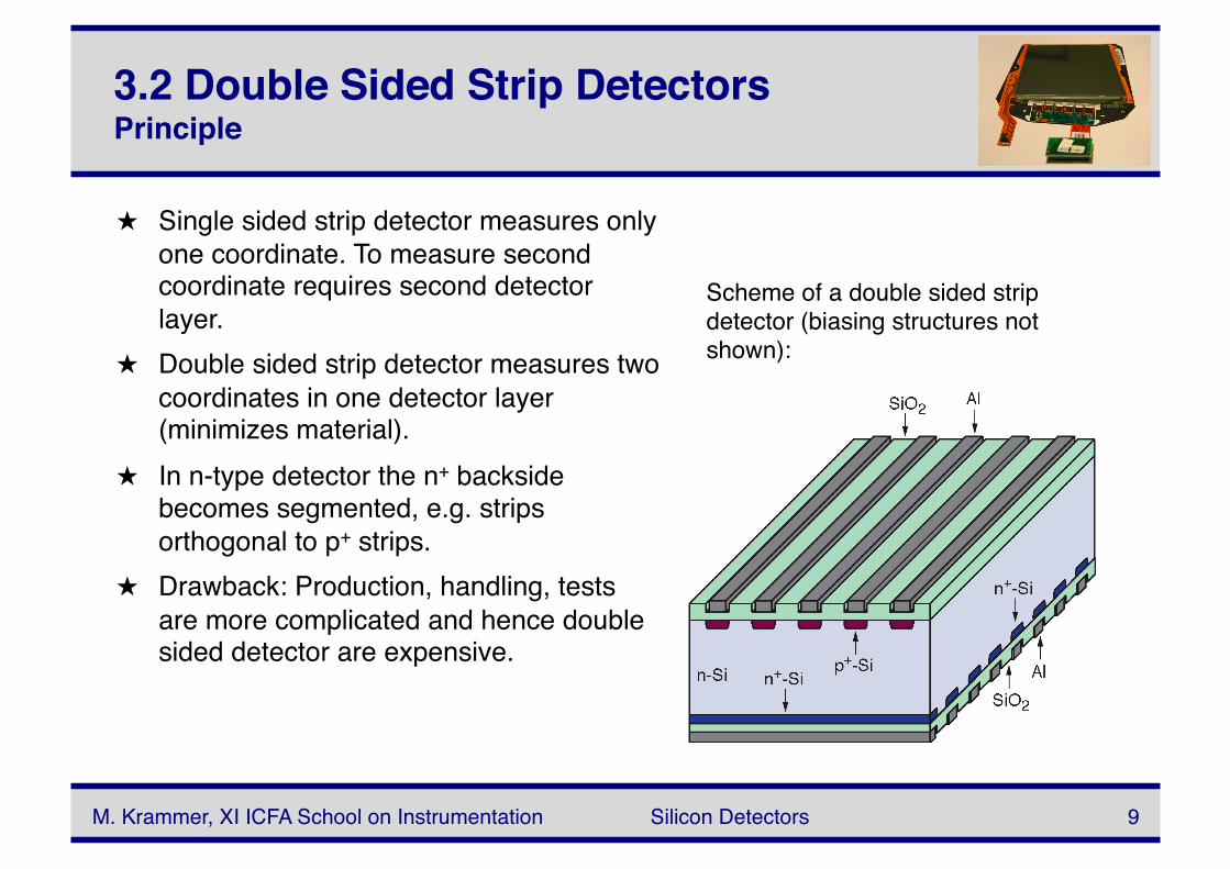
Scheme of a double sided strip detector (biasing structures not shown):
★ Single sided strip detector measures only one coordinate. To measure second coordinate requires second detector layer.
★ Double sided strip detector measures two coordinates in one detector layer (minimizes material).
★ In n-type detector the n+ backside becomes segmented, e.g. strips orthogonal to p+ strips.
★ Drawback: Production, handling, tests are more complicated and hence double sided detector are expensive.
3.2 Double Sided Strip DetectorsPrinciple
M. Krammer, XI ICFA School on Instrumentation Silicon Detectors 10
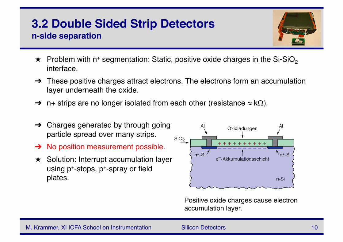
3.2 Double Sided Strip Detectorsn-side separation
★ Problem with n+ segmentation: Static, positive oxide charges in the Si-SiO2 interface.
➔ These positive charges attract electrons. The electrons form an accumulation layer underneath the oxide.
➔ n+ strips are no longer isolated from each other (resistance ≈ kΩ).
Positive oxide charges cause electron accumulation layer.
➔ Charges generated by through going particle spread over many strips.
➔ No position measurement possible. ★ Solution: Interrupt accumulation layer
using p+-stops, p+-spray or field plates.
M. Krammer, XI ICFA School on Instrumentation Silicon Detectors 11
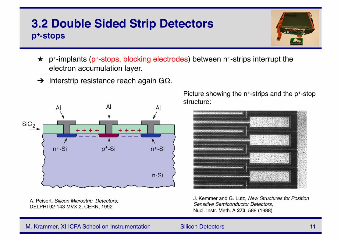
3.2 Double Sided Strip Detectorsp+-stops
★ p+-implants (p+-stops, blocking electrodes) between n+-strips interrupt the electron accumulation layer.
➔ Interstrip resistance reach again GΩ.
A. Peisert, Silicon Microstrip Detectors, DELPHI 92-143 MVX 2, CERN, 1992
Picture showing the n+-strips and the p+-stop structure:
J. Kemmer and G. Lutz, New Structures for Position Sensitive Semiconductor Detectors, Nucl. Instr. Meth. A 273, 588 (1988)
M. Krammer, XI ICFA School on Instrumentation Silicon Detectors 12
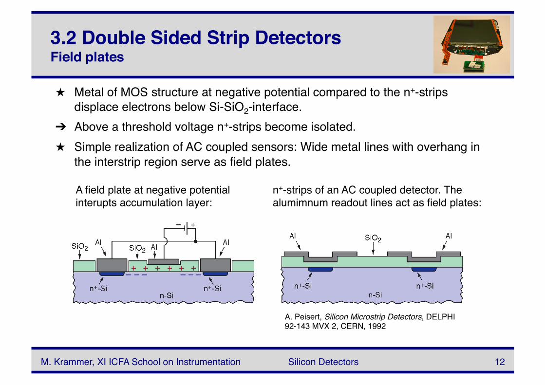
3.2 Double Sided Strip DetectorsField plates
★ Metal of MOS structure at negative potential compared to the n+-strips displace electrons below Si-SiO2-interface.
➔ Above a threshold voltage n+-strips become isolated. ★ Simple realization of AC coupled sensors: Wide metal lines with overhang in
the interstrip region serve as field plates.
n+-strips of an AC coupled detector. The alumimnum readout lines act as field plates:
A. Peisert, Silicon Microstrip Detectors, DELPHI 92-143 MVX 2, CERN, 1992
A field plate at negative potential interupts accumulation layer:
M. Krammer, XI ICFA School on Instrumentation Silicon Detectors 13
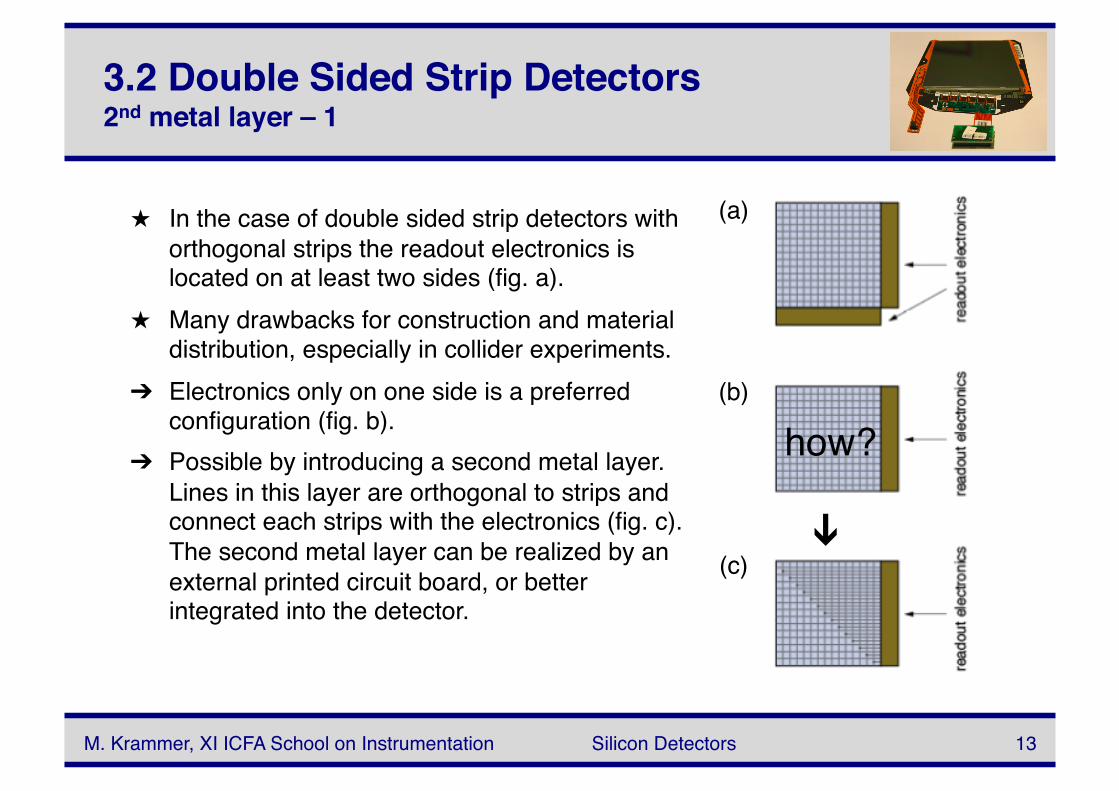
3.2 Double Sided Strip Detectors2nd metal layer – 1
★ In the case of double sided strip detectors with orthogonal strips the readout electronics is located on at least two sides (fig. a).
★ Many drawbacks for construction and material distribution, especially in collider experiments.
➔ Electronics only on one side is a preferred configuration (fig. b).
➔ Possible by introducing a second metal layer. Lines in this layer are orthogonal to strips and connect each strips with the electronics (fig. c). The second metal layer can be realized by an external printed circuit board, or better integrated into the detector.
(a)
(b)
(c)
➔
how?

M. Krammer, XI ICFA School on Instrumentation Silicon Detectors 14
3.2 Double Sided Strip Detectors2nd metal layer – 2
3D scheme of an AC coupled double sided strip detector with 2nd metal readout lines (bias structure not shown). The isolation between the two metal layers is either polyimide or SiO2:
A. Peisert, Silicon Microstrip Detectors, DELPHI 92-143 MVX 2, CERN, 1992
Cross section of the n+ side of an AC coupled double sided strip detector with 2nd metal readout lines. Shown is the end of a strip with the bias resistor:
M. Krammer, XI ICFA School on Instrumentation Silicon Detectors 15
3.3 Hybrid Pixel Detectors Advantage
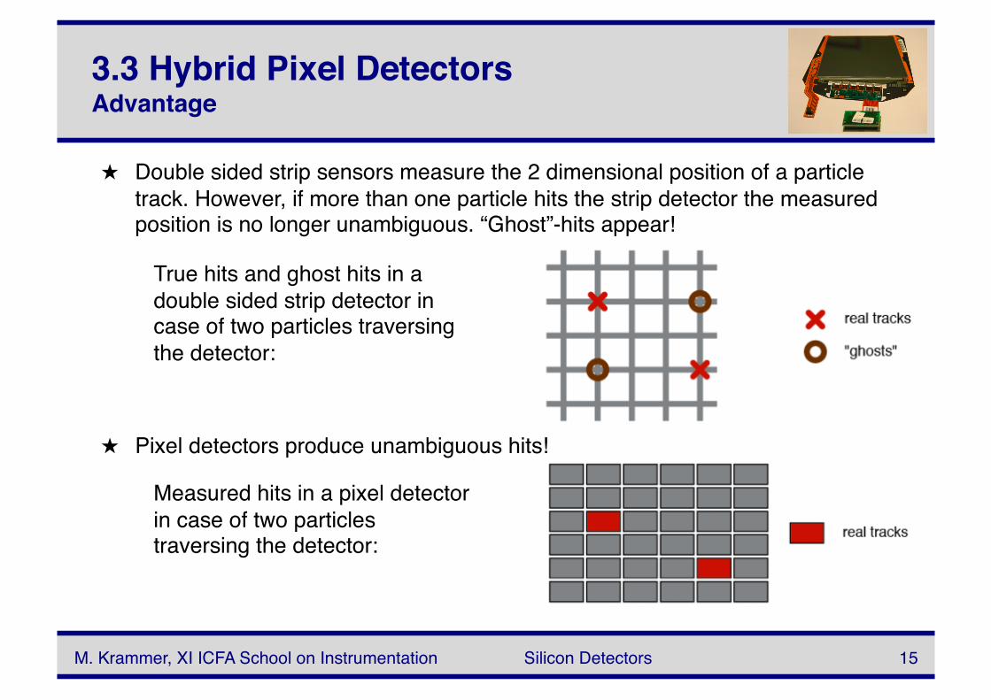
★ Double sided strip sensors measure the 2 dimensional position of a particle track. However, if more than one particle hits the strip detector the measured position is no longer unambiguous. “Ghost”-hits appear!
★ Pixel detectors produce unambiguous hits!
True hits and ghost hits in a double sided strip detector in case of two particles traversing the detector:
Measured hits in a pixel detector in case of two particles traversing the detector:
M. Krammer, XI ICFA School on Instrumentation Silicon Detectors 16
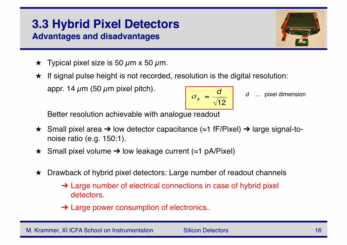
★ Small pixel area ➔ low detector capacitance (≈1 fF/Pixel) ➔ large signal-to-noise ratio (e.g. 150:1).
★ Small pixel volume ➔ low leakage current (≈1 pA/Pixel)
3.3 Hybrid Pixel Detectors Advantages and disadvantages
★ Drawback of hybrid pixel detectors: Large number of readout channels ➔ Large number of electrical connections in case of hybrid pixel
detectors. ➔ Large power consumption of electronics..
★ Typical pixel size is 50 µm x 50 µm. ★ If signal pulse height is not recorded, resolution is the digital resolution:
appr. 14 µm (50 µm pixel pitch).
Better resolution achievable with analogue readout
€
σ x ≈d12
d … pixel dimension
M. Krammer, XI ICFA School on Instrumentation Silicon Detectors 17
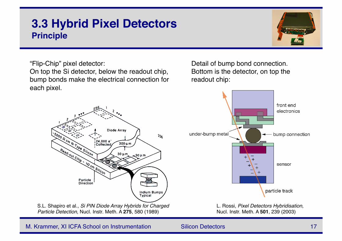
3.3 Hybrid Pixel Detectors Principle
Detail of bump bond connection. Bottom is the detector, on top the readout chip:
“Flip-Chip” pixel detector: On top the Si detector, below the readout chip, bump bonds make the electrical connection for each pixel.
S.L. Shapiro et al., Si PIN Diode Array Hybrids for Charged Particle Detection, Nucl. Instr. Meth. A 275, 580 (1989)
L. Rossi, Pixel Detectors Hybridisation, Nucl. Instr. Meth. A 501, 239 (2003)
M. Krammer, XI ICFA School on Instrumentation Silicon Detectors 18
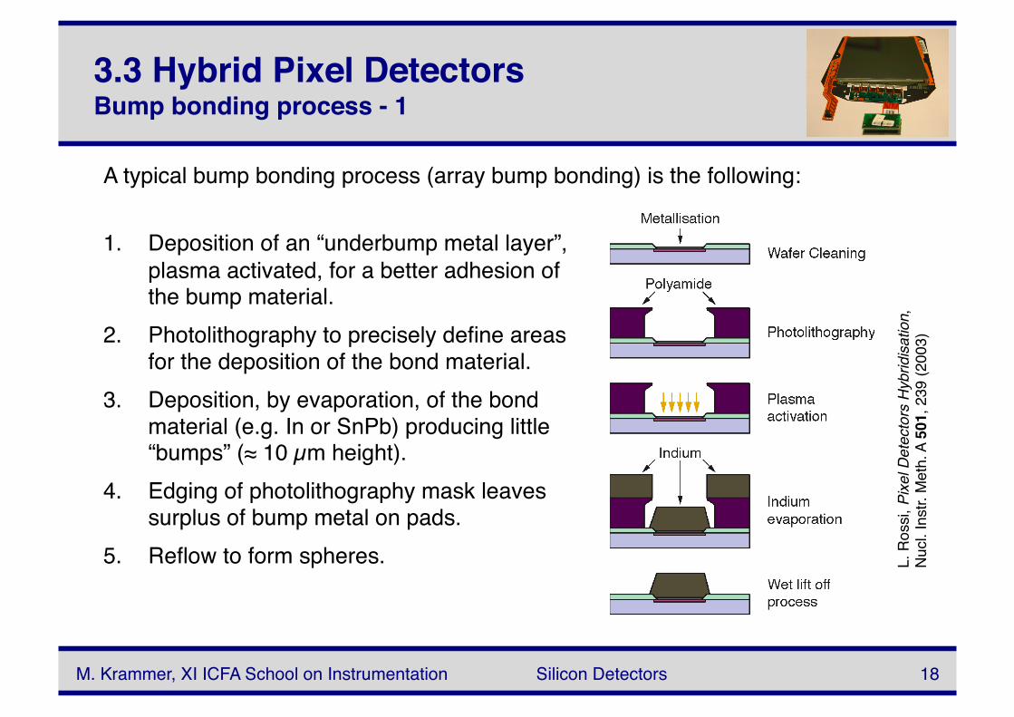
3.3 Hybrid Pixel Detectors Bump bonding process - 1
1. Deposition of an “underbump metal layer”, plasma activated, for a better adhesion of the bump material.
2. Photolithography to precisely define areas for the deposition of the bond material.
3. Deposition, by evaporation, of the bond material (e.g. In or SnPb) producing little “bumps” (≈ 10 µm height).
4. Edging of photolithography mask leaves surplus of bump metal on pads.
5. Reflow to form spheres.
A typical bump bonding process (array bump bonding) is the following:
L. R
ossi,
Pixe
l Det
ecto
rs H
ybrid
isatio
n,
Nucl.
Inst
r. M
eth.
A 5
01, 2
39 (2
003)
M. Krammer, XI ICFA School on Instrumentation Silicon Detectors 19
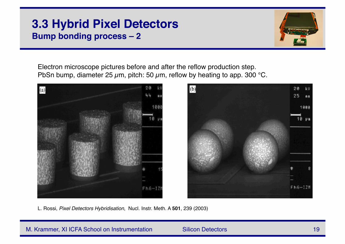
3.3 Hybrid Pixel Detectors Bump bonding process – 2
Electron microscope pictures before and after the reflow production step. PbSn bump, diameter 25 µm, pitch: 50 µm, reflow by heating to app. 300 °C.
L. Rossi, Pixel Detectors Hybridisation, Nucl. Instr. Meth. A 501, 239 (2003)
M. Krammer, XI ICFA School on Instrumentation Silicon Detectors 20
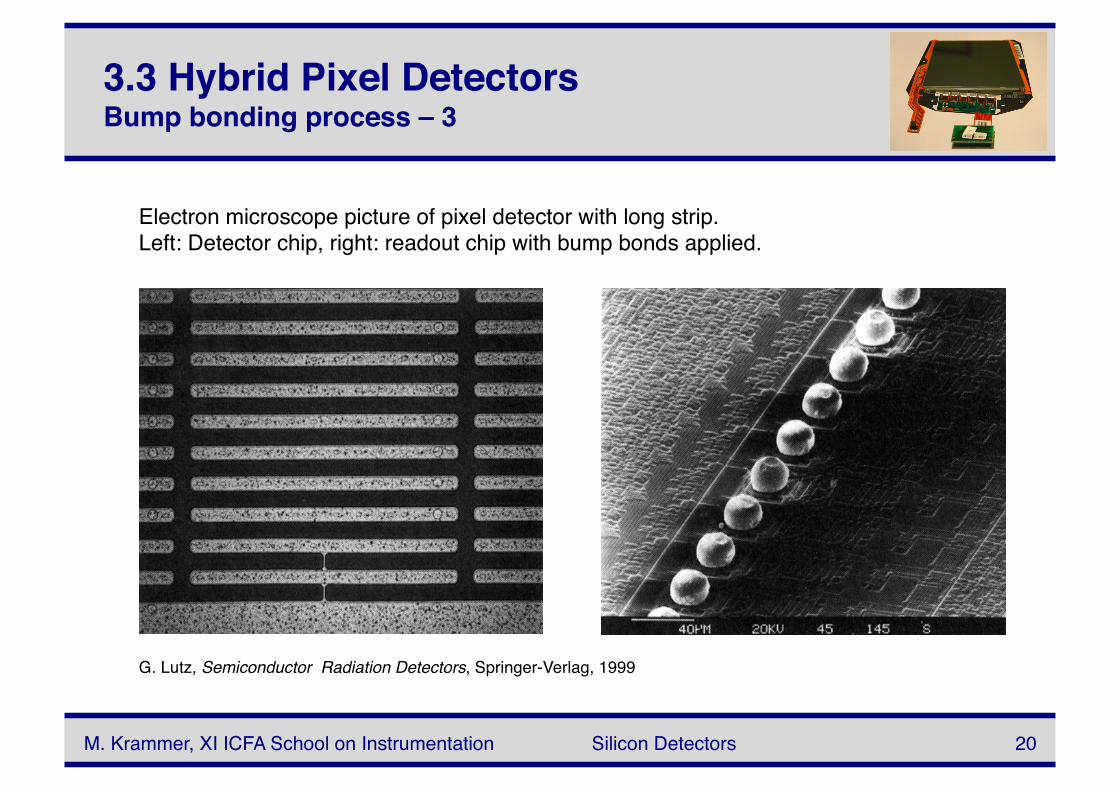
3.3 Hybrid Pixel Detectors Bump bonding process – 3
G. Lutz, Semiconductor Radiation Detectors, Springer-Verlag, 1999
Electron microscope picture of pixel detector with long strip. Left: Detector chip, right: readout chip with bump bonds applied.
21 M. Krammer, XI ICFA School on Instrumentation Silicon Detectors
3.4 – 3.9 Other Si Detector Structures
Strip and hybrid pixel detectors are mature technologies employed in almost every experiment in high energy physics.
Additional interesting silicon detector structures are: • Charged Coupled Devices (CCD)
• Silicon Drift Detectors • Silicon Photo Multiplier (SiPM) • Monolithic Active Pixels (MAPS)
• Depleted Field Effect detectors (DEPFET) • Silicon On Oxide (SOI)
• 3D detectors
22
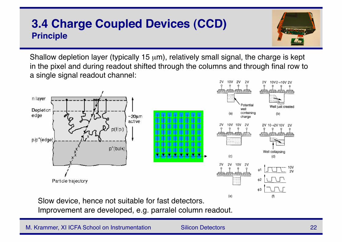
Shallow depletion layer (typically 15 µm), relatively small signal, the charge is kept in the pixel and during readout shifted through the columns and through final row to a single signal readout channel:
M. Krammer, XI ICFA School on Instrumentation Silicon Detectors
3.4 Charge Coupled Devices (CCD)Principle
Slow device, hence not suitable for fast detectors. Improvement are developed, e.g. parralel column readout.
23 M. Krammer, XI ICFA School on Instrumentation Silicon Detectors
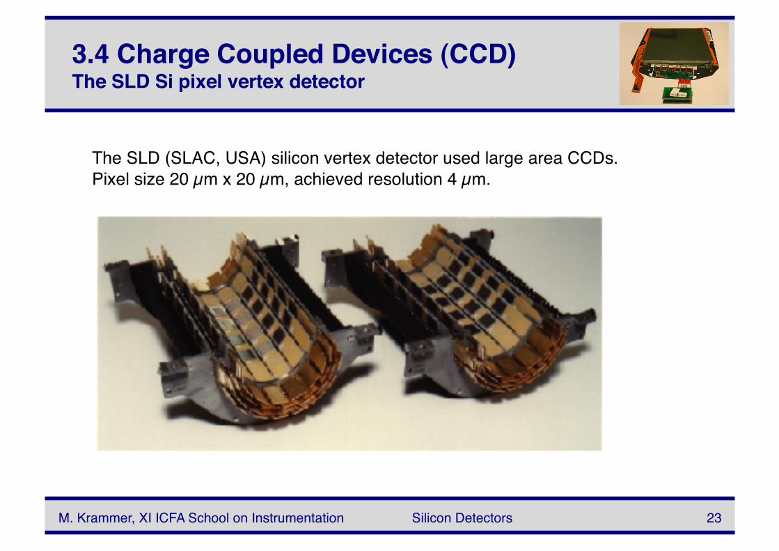
3.4 Charge Coupled Devices (CCD)The SLD Si pixel vertex detector
The SLD (SLAC, USA) silicon vertex detector used large area CCDs. Pixel size 20 µm x 20 µm, achieved resolution 4 µm.
24 M. Krammer, XI ICFA School on Instrumentation Silicon Detectors
3.5 Silicon Drift DetectorsPrinciple
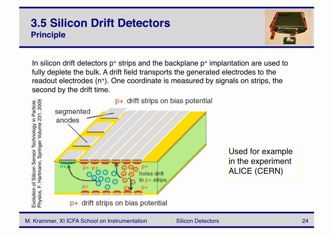
Used for example in the experiment ALICE (CERN)
Evol
utio
n of
Silic
on S
enso
r Tec
hnol
ogy
in P
artic
le
Phys
ics, F
. Har
tman
n, S
prin
ger V
olum
e 23
1, 2
009
In silicon drift detectors p+ strips and the backplane p+ implantation are used to fully deplete the bulk. A drift field transports the generated electrodes to the readout electrodes (n+). One coordinate is measured by signals on strips, the second by the drift time.
M. Krammer, XI ICFA School on Instrumentation Silicon Detectors 25
R. H. Haitz, J. App.Phys. Vol. 36, No. 10 (1965) 3123
3.6 Avalanche Photo Diode (APD)Principle
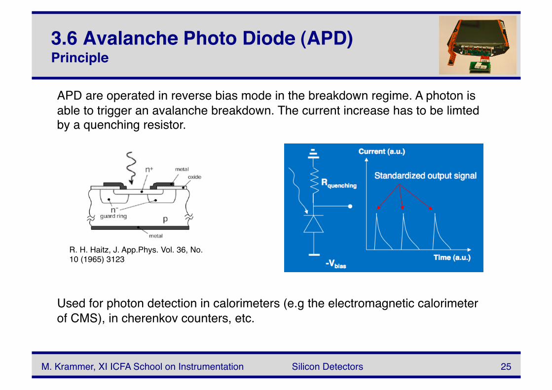
APD are operated in reverse bias mode in the breakdown regime. A photon is able to trigger an avalanche breakdown. The current increase has to be limted by a quenching resistor.
Used for photon detection in calorimeters (e.g the electromagnetic calorimeter of CMS), in cherenkov counters, etc.
M. Krammer, XI ICFA School on Instrumentation Silicon Detectors 26
Al
ARC
-Vbias Back contact
Rquenching
p+ silicon wafer
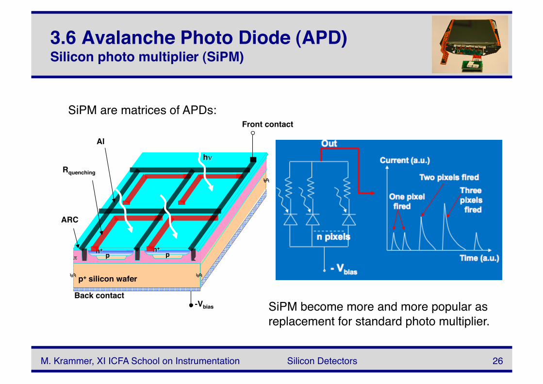
Front contact SiPM are matrices of APDs:
3.6 Avalanche Photo Diode (APD)Silicon photo multiplier (SiPM)
SiPM become more and more popular as replacement for standard photo multiplier.
27
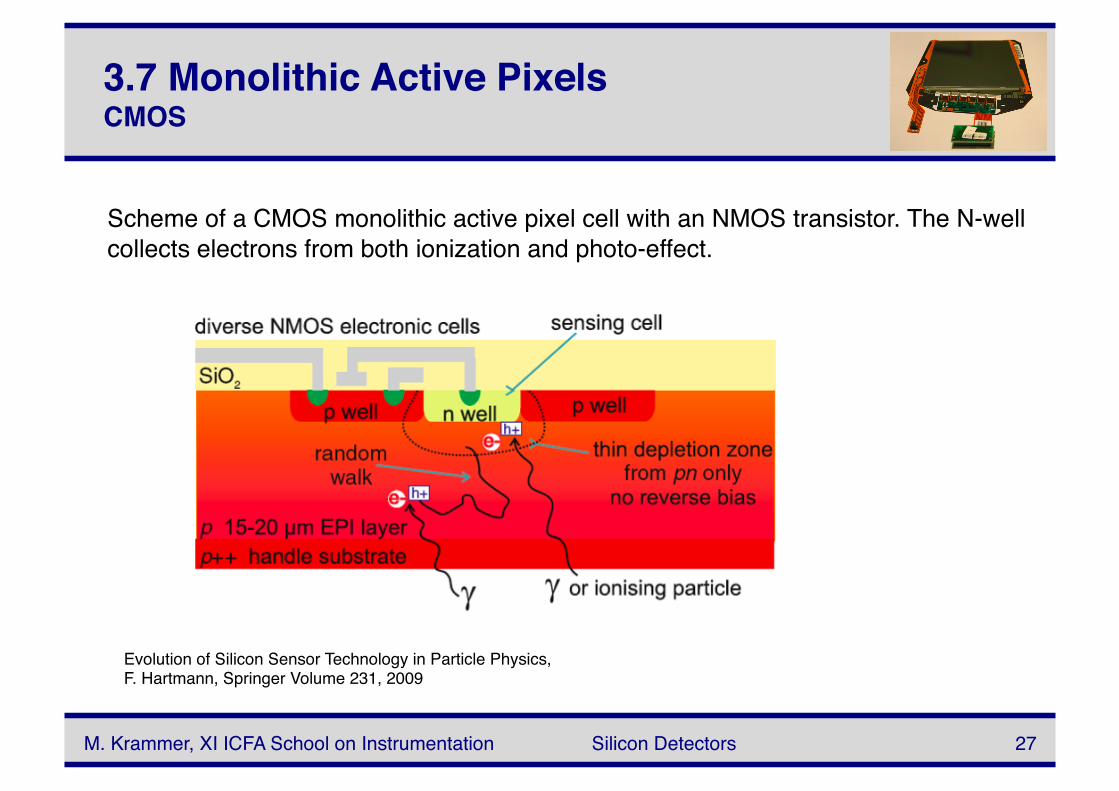
3.7 Monolithic Active PixelsCMOS
M. Krammer, XI ICFA School on Instrumentation Silicon Detectors
Scheme of a CMOS monolithic active pixel cell with an NMOS transistor. The N-well collects electrons from both ionization and photo-effect.
Evolution of Silicon Sensor Technology in Particle Physics, F. Hartmann, Springer Volume 231, 2009

28
3.7 Monolithic Active PixelsSilicon on Insulator (SOI)
M. Krammer, XI ICFA School on Instrumentation Silicon Detectors
A SOI detector consists of a thick full depleted high resitivity bulk and seperated by a layer of SiO2 a low resistivity n-type material. NMOS and PMOs transistors are implemented in the low resitivity material using standard IC methods.
Evolution of Silicon Sensor Technology in Particle Physics, F. Hartmann, Springer Volume 231, 2009
29
Candidate for ILC and Belle II
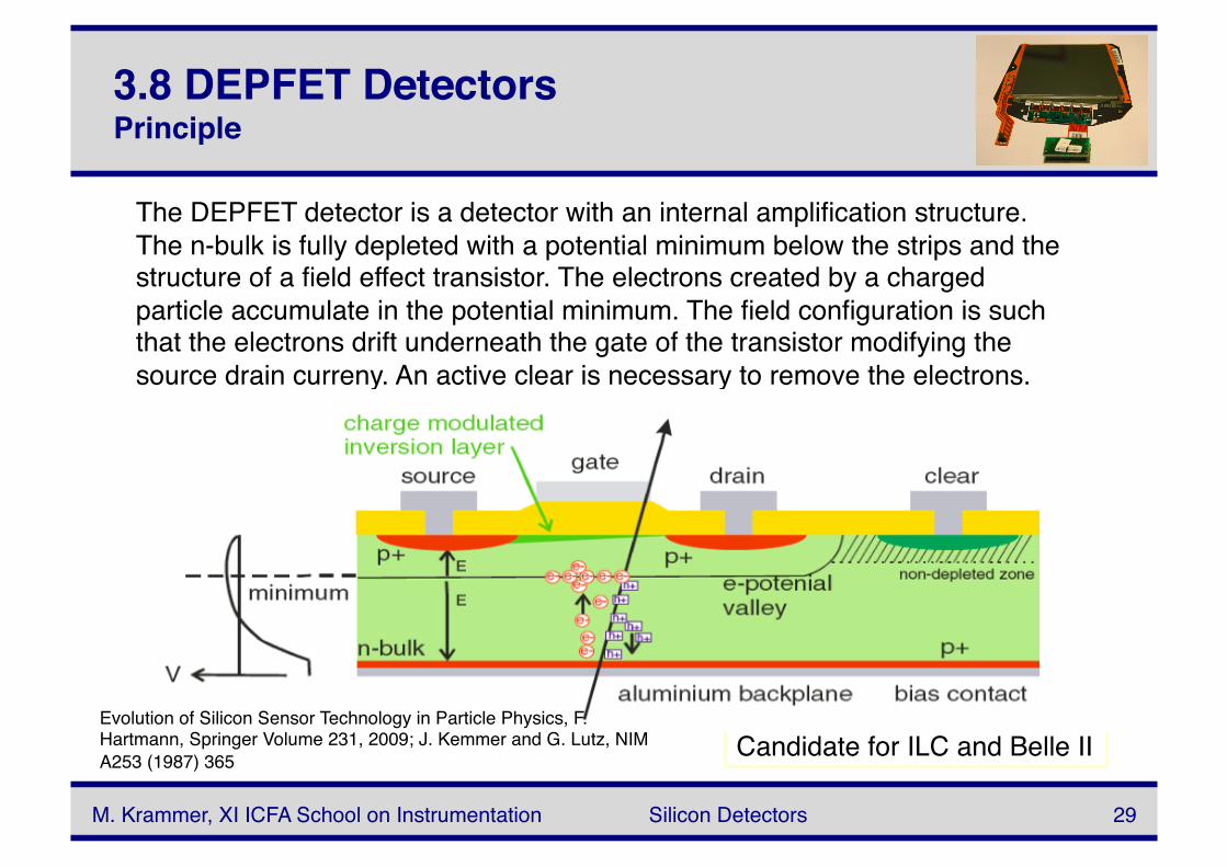
3.8 DEPFET DetectorsPrinciple
M. Krammer, XI ICFA School on Instrumentation Silicon Detectors
The DEPFET detector is a detector with an internal amplification structure. The n-bulk is fully depleted with a potential minimum below the strips and the structure of a field effect transistor. The electrons created by a charged particle accumulate in the potential minimum. The field configuration is such that the electrons drift underneath the gate of the transistor modifying the source drain curreny. An active clear is necessary to remove the electrons.
Evolution of Silicon Sensor Technology in Particle Physics, F. Hartmann, Springer Volume 231, 2009; J. Kemmer and G. Lutz, NIM A253 (1987) 365
30
Very radiation tolerant detectors, in discussion for inner detector layers at SLHC.
M. Krammer, XI ICFA School on Instrumentation Silicon Detectors
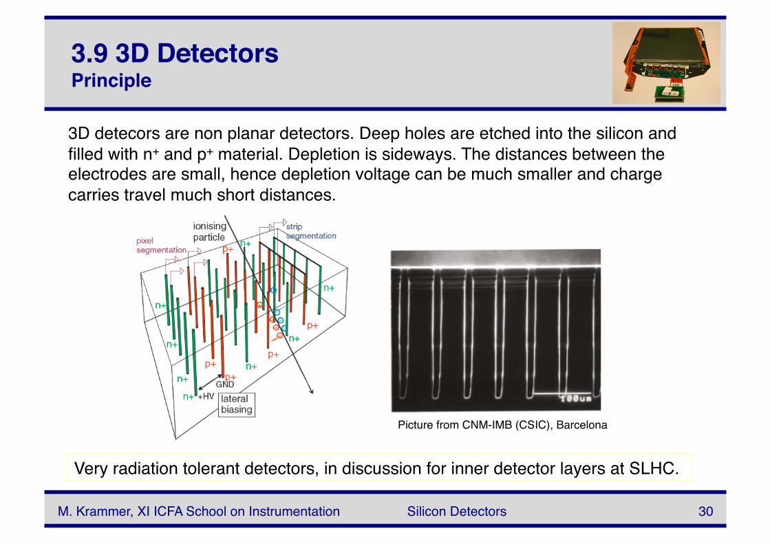
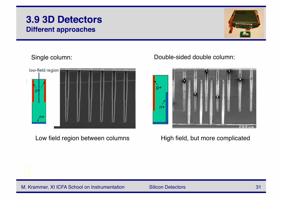
3.9 3D DetectorsPrinciple
3D detecors are non planar detectors. Deep holes are etched into the silicon and filled with n+ and p+ material. Depletion is sideways. The distances between the electrodes are small, hence depletion voltage can be much smaller and charge carries travel much short distances.
Picture from CNM-IMB (CSIC), Barcelona
31 M. Krammer, XI ICFA School on Instrumentation Silicon Detectors
3.9 3D DetectorsDifferent approaches
Single column: Double-sided double column:
Low field region between columns High field, but more complicated
M. Krammer, XI ICFA School on Instrumentation Silicon Detectors 32
4 Performance
4.1 Signal to Noise Ratio Introduction
M. Krammer, XI ICFA School on Instrumentation Silicon Detectors 33
The signal generated in a silicon detector depends essentially only on the thickness of the depletion zone and on the dE/dx of the particle.
The noise in a silicon detector system depends on various parameters: geometry of the detector, the biasing scheme, the readout electronics, etc.
Noise is typically given as “equivalent noise charge” ENC. This is the noise at the input of the amplifier in elementary charges.
4.1 Signal to Noise Ratio Noise contributions
M. Krammer, XI ICFA School on Instrumentation Silicon Detectors 34
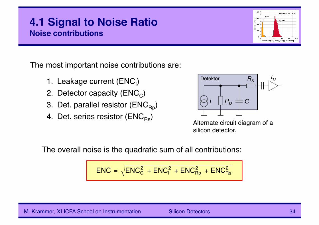
1. Leakage current (ENCI) 2. Detector capacity (ENCC) 3. Det. parallel resistor (ENCRp) 4. Det. series resistor (ENCRs)
The most important noise contributions are:
The overall noise is the quadratic sum of all contributions:
€
ENC = ENCC2 + ENCI
2 + ENCRp2 + ENCRs
2
Alternate circuit diagram of a silicon detector.
4.1 Noise ContributionsLeakage current - 1
M. Krammer, XI ICFA School on Instrumentation Silicon Detectors 35
The detector leakage current comes from thermally generated electron holes pairs within the depletion region. These charges are seperated by the electric field and generate the leakage current. The fluctuations of this current are the source of noise.
In a typical detector system (good detector quality, no irradiation damage) the leakage current noise is usually negligible.
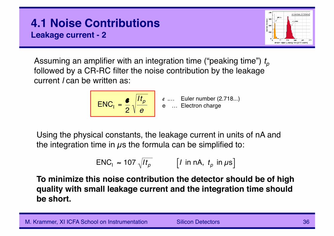
4.1 Noise ContributionsLeakage current - 2
M. Krammer, XI ICFA School on Instrumentation Silicon Detectors 36
Assuming an amplifier with an integration time (“peaking time”) tp followed by a CR-RC filter the noise contribution by the leakage current l can be written as:
Using the physical constants, the leakage current in units of nA and the integration time in µs the formula can be simplified to:
€
ENCI =e2
I tpe
To minimize this noise contribution the detector should be of high quality with small leakage current and the integration time should be short. €
ENCI ≈ 107 I tp I in nA, tp in µs[ ]
e .… Euler number (2.718...) e … Electron charge
4.1 Noise ContributionsDetector capacity
M. Krammer, XI ICFA School on Instrumentation Silicon Detectors 37
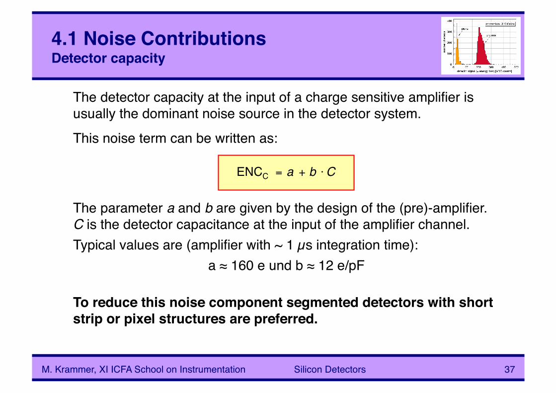
The detector capacity at the input of a charge sensitive amplifier is usually the dominant noise source in the detector system. This noise term can be written as:
The parameter a and b are given by the design of the (pre)-amplifier. C is the detector capacitance at the input of the amplifier channel. Typical values are (amplifier with ~ 1 µs integration time):
a ≈ 160 e und b ≈ 12 e/pF
€
ENCC = a + b ⋅C
To reduce this noise component segmented detectors with short strip or pixel structures are preferred.
4.1 Noise ContributionsParallel resistor
M. Krammer, XI ICFA School on Instrumentation Silicon Detectors 38
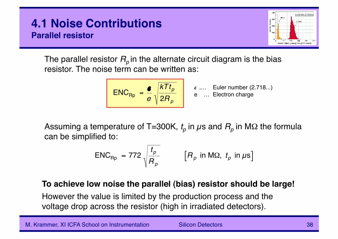
The parallel resistor Rp in the alternate circuit diagram is the bias resistor. The noise term can be written as:
Assuming a temperature of T=300K, tp in µs and Rp in MΩ the formula can be simplified to:
€
ENCRp =ee
kTtp2Rp
To achieve low noise the parallel (bias) resistor should be large! However the value is limited by the production process and the voltage drop across the resistor (high in irradiated detectors).
€
ENCRp ≈ 772tpR p
Rp in MΩ, tp in µs[ ]
e .… Euler number (2.718...) e … Electron charge
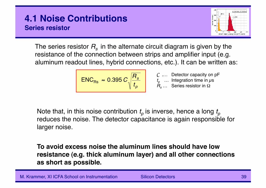
4.1 Noise ContributionsSeries resistor
M. Krammer, XI ICFA School on Instrumentation Silicon Detectors 39
The series resistor Rs in the alternate circuit diagram is given by the resistance of the connection between strips and amplifier input (e.g. aluminum readout lines, hybrid connections, etc.). It can be written as:
Note that, in this noise contribution tp is inverse, hence a long tp reduces the noise. The detector capacitance is again responsible for larger noise.
To avoid excess noise the aluminum lines should have low resistance (e.g. thick aluminum layer) and all other connections as short as possible.
€
ENCRs ≈ 0.395C Rstp
C .… Detector capacity on pF tp … Integration time in µs Rs … Series resistor in Ω
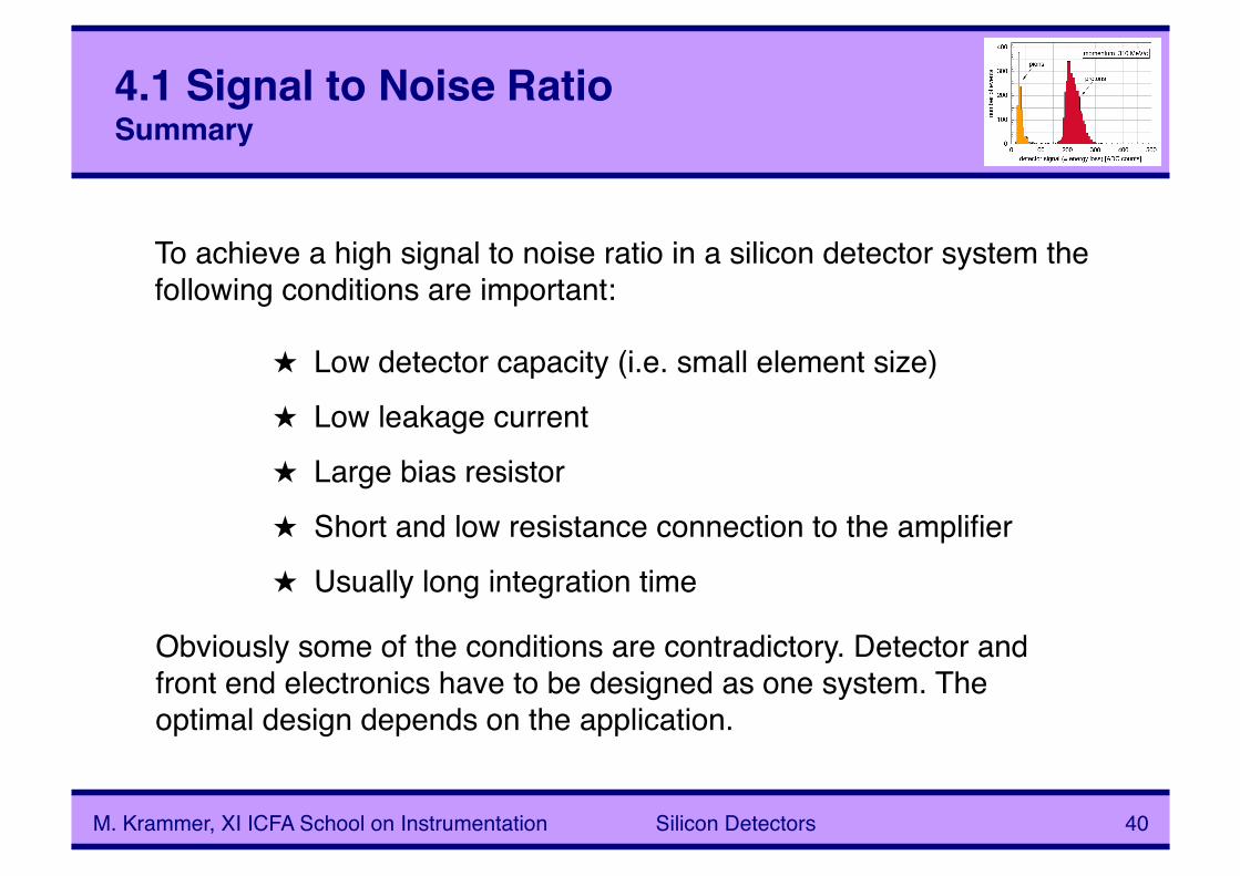
4.1 Signal to Noise RatioSummary
M. Krammer, XI ICFA School on Instrumentation Silicon Detectors 40
★ Low detector capacity (i.e. small element size) ★ Low leakage current ★ Large bias resistor ★ Short and low resistance connection to the amplifier ★ Usually long integration time
To achieve a high signal to noise ratio in a silicon detector system the following conditions are important:
Obviously some of the conditions are contradictory. Detector and front end electronics have to be designed as one system. The optimal design depends on the application.
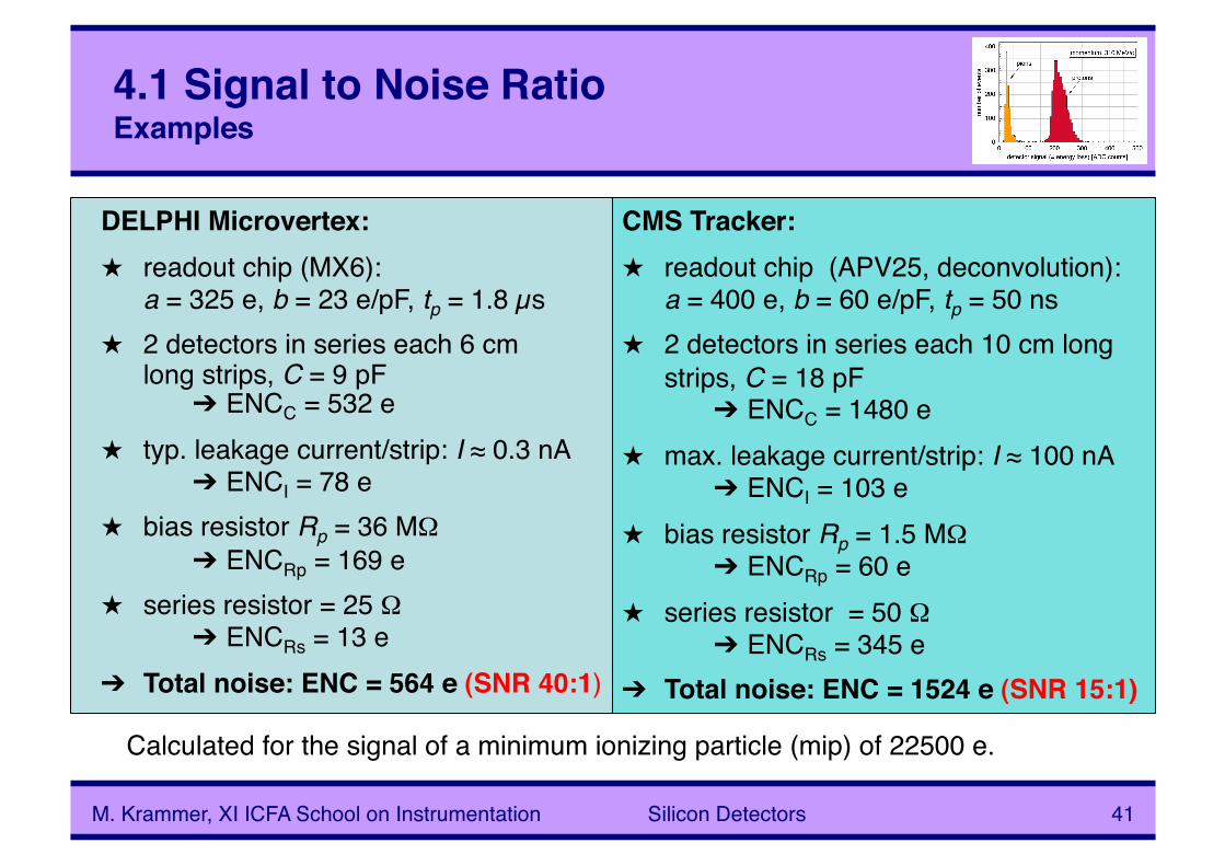
4.1 Signal to Noise RatioExamples
M. Krammer, XI ICFA School on Instrumentation Silicon Detectors 41
Calculated for the signal of a minimum ionizing particle (mip) of 22500 e.
DELPHI Microvertex: ★ readout chip (MX6):
a = 325 e, b = 23 e/pF, tp = 1.8 µs ★ 2 detectors in series each 6 cm
long strips, C = 9 pF ➔ ENCC = 532 e
★ typ. leakage current/strip: I ≈ 0.3 nA ➔ ENCI = 78 e
★ bias resistor Rp = 36 MΩ ➔ ENCRp = 169 e
★ series resistor = 25 Ω ➔ ENCRs = 13 e
➔ Total noise: ENC = 564 e (SNR 40:1)
CMS Tracker: ★ readout chip (APV25, deconvolution):
a = 400 e, b = 60 e/pF, tp = 50 ns ★ 2 detectors in series each 10 cm long
strips, C = 18 pF ➔ ENCC = 1480 e
★ max. leakage current/strip: I ≈ 100 nA ➔ ENCI = 103 e
★ bias resistor Rp = 1.5 MΩ ➔ ENCRp = 60 e
★ series resistor = 50 Ω ➔ ENCRs = 345 e
➔ Total noise: ENC = 1524 e (SNR 15:1)
4.2 Position ResolutionIntroduction
M. Krammer, XI ICFA School on Instrumentation Silicon Detectors 42
★ Physics processes: – Statistical fluctuations of the energy loss – Diffusion of charge carriers
★ External parameter: – Binary readout (thresh hold counter) or read out of
analogue signal value – Distance between strips (strip pitch) – Signal to noise ratio
The position resolution – the main parameter of a position detector – depends on various factors, some due to physics constraints and some due to the design of the system (external parameters).
4.2 Position ResolutionStatistical fluctuation of the energy loss – 1
M. Krammer, XI ICFA School on Instrumentation Silicon Detectors 43
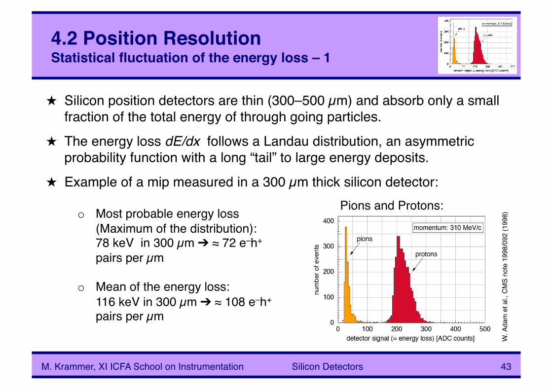
★ Silicon position detectors are thin (300–500 µm) and absorb only a small fraction of the total energy of through going particles.
★ The energy loss dE/dx follows a Landau distribution, an asymmetric probability function with a long “tail” to large energy deposits.
★ Example of a mip measured in a 300 µm thick silicon detector: Pions and Protons:
W. A
dam
et a
l., C
MS
note
199
8/09
2 (1
998) o Most probable energy loss
(Maximum of the distribution): 78 keV in 300 µm ➔ ≈ 72 e–h+ pairs per µm
o Mean of the energy loss: 116 keV in 300 µm ➔ ≈ 108 e–h+ pairs per µm
4.2 Position ResolutionStatistical fluctuation of the energy loss – 3
M. Krammer, XI ICFA School on Instrumentation Silicon Detectors 44
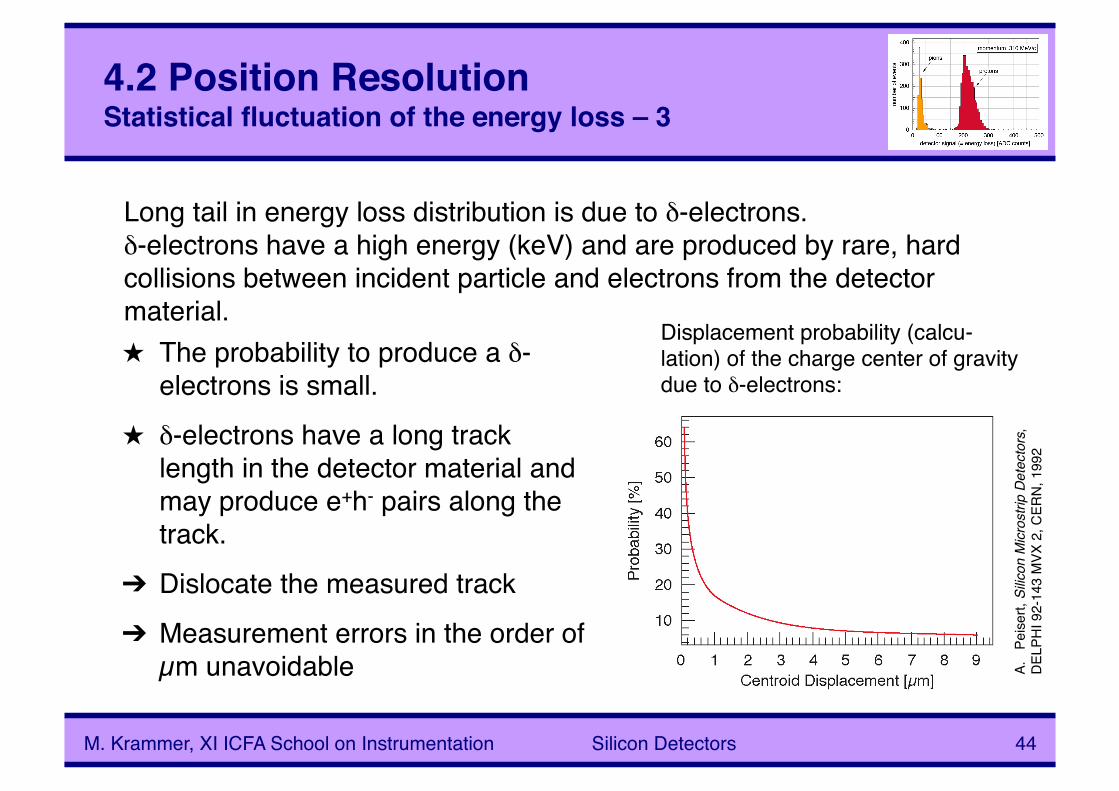
★ The probability to produce a δ-electrons is small.
★ δ-electrons have a long track length in the detector material and may produce e+h- pairs along the track.
➔ Dislocate the measured track ➔ Measurement errors in the order of
µm unavoidable
Long tail in energy loss distribution is due to δ-electrons. δ-electrons have a high energy (keV) and are produced by rare, hard collisions between incident particle and electrons from the detector material.
Displacement probability (calcu-lation) of the charge center of gravity due to δ-electrons:
A.
Peise
rt, S
ilicon
Micr
ostri
p De
tect
ors,
DE
LPHI
92-
143
MVX
2, C
ERN,
199
2
4.2 Position ResolutionDiffusion – 1
M. Krammer, XI ICFA School on Instrumentation Silicon Detectors 45
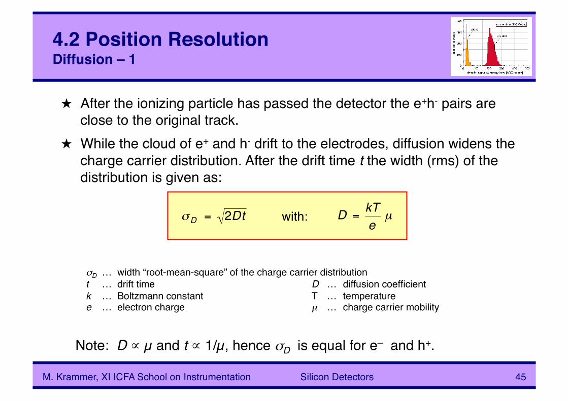
★ After the ionizing particle has passed the detector the e+h- pairs are close to the original track.
★ While the cloud of e+ and h- drift to the electrodes, diffusion widens the charge carrier distribution. After the drift time t the width (rms) of the distribution is given as:
Note: D ∝ µ and t ∝ 1/µ, hence σD is equal for e– and h+.
σD … width “root-mean-square” of the charge carrier distribution t … drift time D … diffusion coefficient k … Boltzmann constant T … temperature e … electron charge µ … charge carrier mobility
€
σD = 2Dt with:
€
D =kTe
µ
4.2 Position ResolutionDiffusion – 2
M. Krammer, XI ICFA School on Instrumentation Silicon Detectors 46
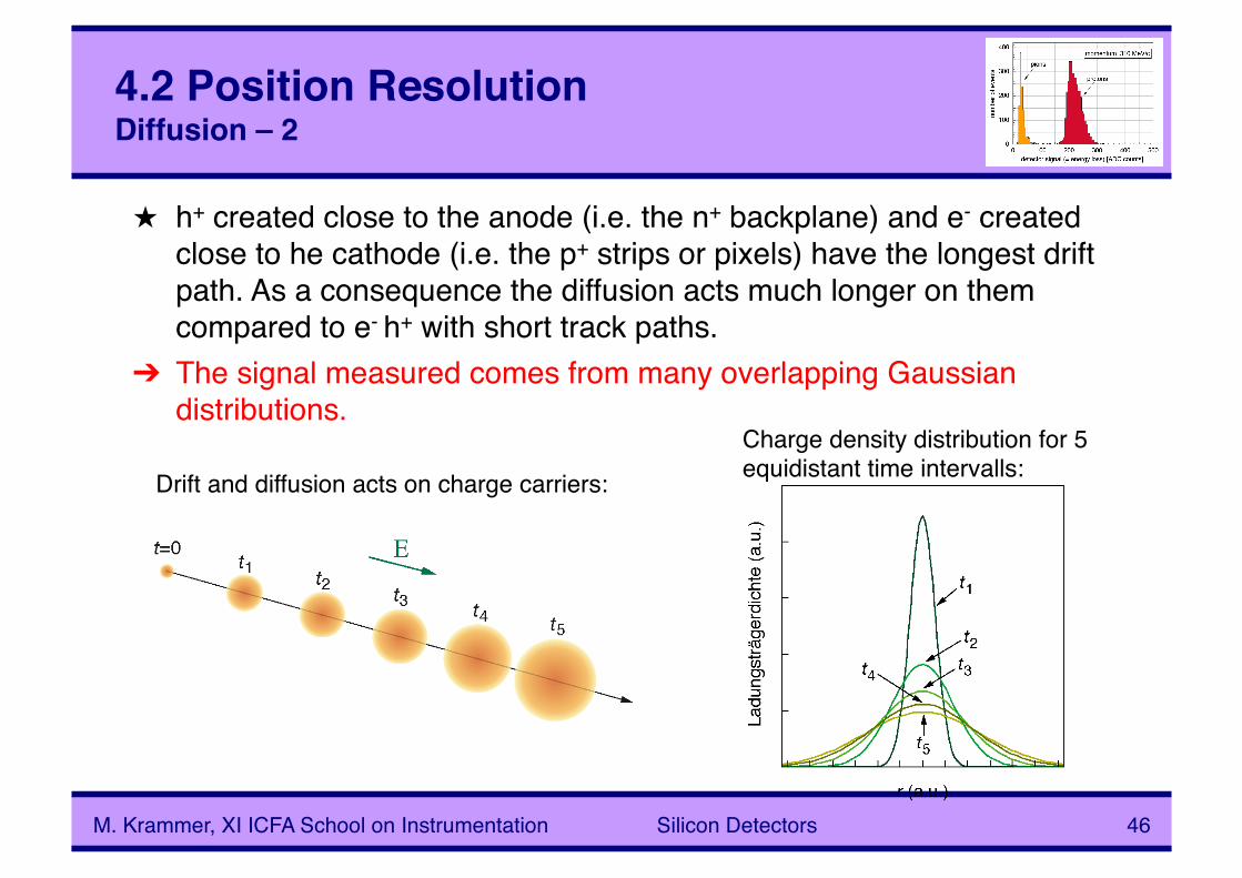
★ h+ created close to the anode (i.e. the n+ backplane) and e- created close to he cathode (i.e. the p+ strips or pixels) have the longest drift path. As a consequence the diffusion acts much longer on them compared to e- h+ with short track paths.
➔ The signal measured comes from many overlapping Gaussian distributions.
Drift and diffusion acts on charge carriers:
Charge density distribution for 5 equidistant time intervalls:
4.2 Position ResolutionDiffusion – 3
M. Krammer, XI ICFA School on Instrumentation Silicon Detectors 47
★ Diffusion widens the charge cloud. However, this has an positive effect on the position resolution! ➔ charge is distributed over more than one strip, with interpolation (calculation of the charge center of gravity) a better position measurement is achievable.
★ This is only possible if analogue read out of the signal is implemented. ★ Interpolation is more precise the larger the signal to noise ratio is. ➔ Strip pitch and signal to noise ratio determine the position resolution.
★ Larger charge sharing can also be achieved by tilting the detector.
4.2 Position ResolutionThreshold readout versus analogue readout
M. Krammer, XI ICFA School on Instrumentation Silicon Detectors 48
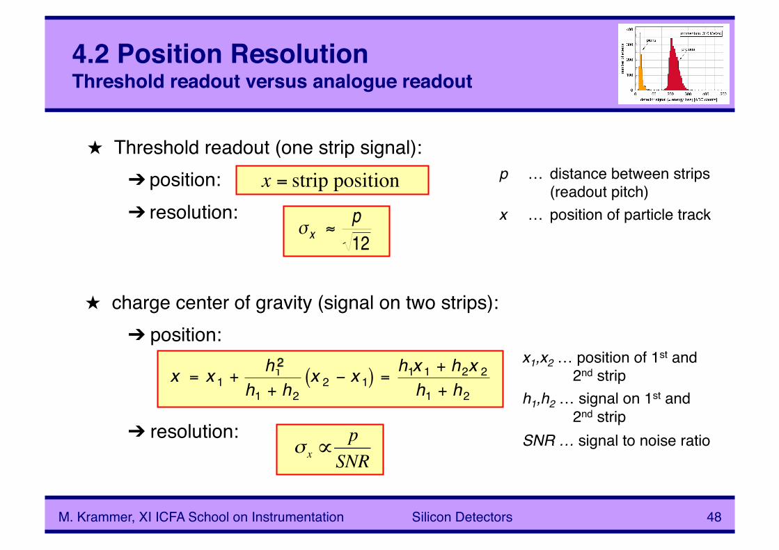
★ charge center of gravity (signal on two strips): ➔ position:
➔ resolution: €
x = x 1 +h1
h1 + h2x 2 − x 1( ) =
h1x 1 + h2x 2h1 + h2
€
σ x ≈p
SNR
p … distance between strips (readout pitch)
x … position of particle track
★ Threshold readout (one strip signal): ➔ position: ➔ resolution:
€
σ x ≈p12
€
x = strip position
x1,x2 … position of 1st and 2nd strip
h1,h2 … signal on 1st and 2nd strip
SNR … signal to noise ratio
€
∝
4.2 Position ResolutionIntermediate strips – 1
M. Krammer, XI ICFA School on Instrumentation Silicon Detectors 49
★ The strip pitch determines to a large extend the position resolution. With small strip pitch a better position resolution is achievable. ➔ small strip pitch requires large number of electronic channels ➔ cost increase ➔ power dissipation increase
★ A possible solution is the implementation of intermediate strips. These are strips not connected to the readout electronics located between readout strips. The signal from these intermediate strips is transferred by capacitive coupling to the readout strips. ➔ more hits with signals on more than one strip ➔ Improved resolution with smaller number of readout channels.
4.2 Position ResolutionIntermediate strips – 2
M. Krammer, XI ICFA School on Instrumentation Silicon Detectors 50
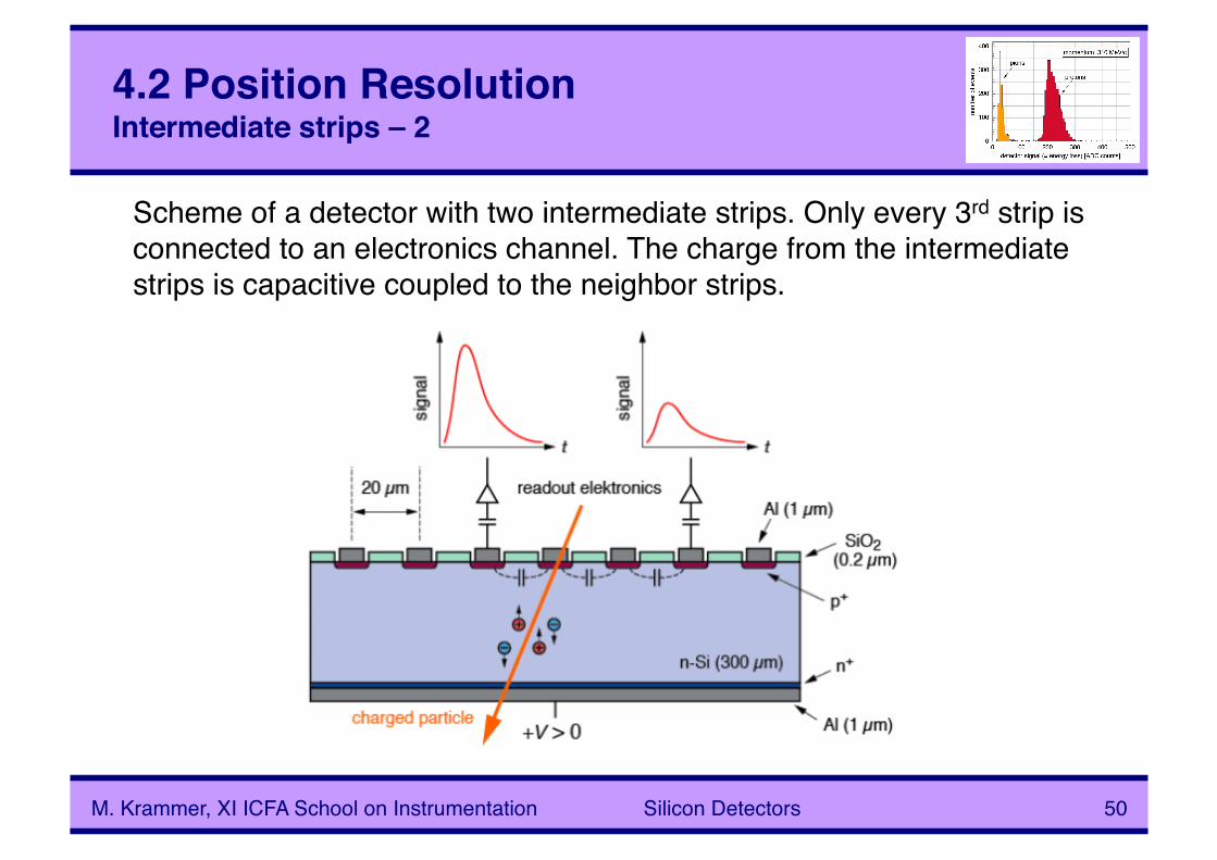
Scheme of a detector with two intermediate strips. Only every 3rd strip is connected to an electronics channel. The charge from the intermediate strips is capacitive coupled to the neighbor strips.
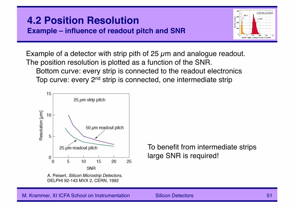
4.2 Position ResolutionExample – influence of readout pitch and SNR
M. Krammer, XI ICFA School on Instrumentation Silicon Detectors 51
Example of a detector with strip pith of 25 µm and analogue readout. The position resolution is plotted as a function of the SNR. Bottom curve: every strip is connected to the readout electronics Top curve: every 2nd strip is connected, one intermediate strip
To benefit from intermediate strips large SNR is required!
A. Peisert, Silicon Microstrip Detectors, DELPHI 92-143 MVX 2, CERN, 1992