2x1W stereo audio power amplifier with active low standby mode · class stereo audio applications....
29
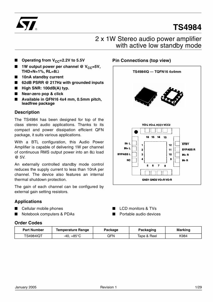
January 2005 Revision 1 1/29 ■ Operating from V CC =2.2V to 5.5V ■ 1W output power per channel @ V CC =5V, THD+N=1%, RL=8Ω ■ 10nA standby current ■ 62dB PSRR @ 217Hz with grounded inputs ■ High SNR: 100dB(A) typ. ■ Near-zero pop & click ■ Available in QFN16 4x4 mm, 0.5mm pitch, leadfree package Description The TS4984 has been designed for top of the class stereo audio applications. Thanks to its compact and power dissipation efficient QFN package, it suits various applications. With a BTL configuration, this Audio Power Amplifier is capable of delivering 1W per channel of continuous RMS output power into an 8Ω load @ 5V. An externally controlled standby mode control reduces the supply current to less than 10nA per channel. The device also features an internal thermal shutdown protection. The gain of each channel can be configured by external gain setting resistors. Pin Connections (top view) Applications ■ Cellular mobile phones ■ Notebook computers & PDAs ■ LCD monitors & TVs ■ Portable audio devices Order Codes TS4984IQ — TQFN16 4x4mm 1 2 3 4 5 6 7 8 12 11 10 9 16 15 14 13 IN- L IN+ L BYPASS L NC GND1 GND2 VO+R VO-R IN+ R IN- R BYPASS R STBY VCC2 VCC1 VO+L VO-L 1 2 3 4 5 6 7 8 12 11 10 9 16 15 14 13 16 15 14 13 IN- L IN+ L BYPASS L NC GND1 GND2 VO+R VO-R IN+ R IN- R BYPASS R STBY VCC2 VCC1 VO+L VO-L Part Number Temperature Range Package Packaging Marking TS4984IQT -40, +85°C QFN Tape & Reel K984 TS4984 2 x 1W Stereo audio power amplifier with active low standby mode
Transcript of 2x1W stereo audio power amplifier with active low standby mode · class stereo audio applications....
TS49842 x 1W Stereo audio power amplifier
with active low standby mode
Operating from VCC=2.2V to 5.5V
1W output power per channel @ VCC=5V, THD+N=1%, RL=8Ω
10nA standby current 62dB PSRR @ 217Hz with grounded inputs High SNR: 100dB(A) typ. Near-zero pop & click Available in QFN16 4x4 mm, 0.5mm pitch,
leadfree package
Description
The TS4984 has been designed for top of theclass stereo audio applications. Thanks to itscompact and power dissipation efficient QFNpackage, it suits various applications.
With a BTL configuration, this Audio PowerAmplifier is capable of delivering 1W per channelof continuous RMS output power into an 8Ω load@ 5V.
An externally controlled standby mode controlreduces the supply current to less than 10nA perchannel. The device also features an internalthermal shutdown protection.
The gain of each channel can be configured byexternal gain setting resistors.
Pin Connections (top view)
Applications
Cellular mobile phones Notebook computers & PDAs
LCD monitors & TVs Portable audio devices
Order Codes
TS4984IQ — TQFN16 4x4mm
1
2
3
4
5 6 7 8
12
11
10
9
16 15 14 13
IN- L
IN+ L
BYPASS L
NC
GND1 GND2 VO+R VO-R
IN+ R
IN- R
BYPASS R
STBY
VCC2VCC1VO+LVO-L
1
2
3
4
5 6 7 8
12
11
10
9
16 15 14 1316 15 14 13
IN- L
IN+ L
BYPASS L
NC
GND1 GND2 VO+R VO-R
IN+ R
IN- R
BYPASS R
STBY
VCC2VCC1VO+LVO-L
Part Number Temperature Range Package Packaging Marking
TS4984IQT -40, +85°C QFN Tape & Reel K984
January 2005 Revision 1 1/29
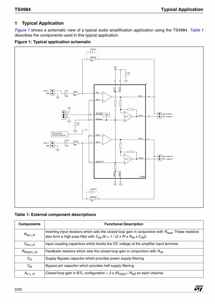
TS4984 Typical Application
1 Typical Application
Figure 1 shows a schematic view of a typical audio amplification application using the TS4984. Table 1describes the components used in this typical application.
Figure 1: Typical application schematic
Table 1: External component descriptions
Components Functional Description
RIN L,RInverting input resistors which sets the closed loop gain in conjunction with Rfeed. These resistors also form a high pass filter with CIN (fc = 1 / (2 x Pi x RIN x CIN)).
CIN L,R Input coupling capacitors which blocks the DC voltage at the amplifier input terminal.
RFEED L,R Feedback resistors which sets the closed loop gain in conjunction with RIN.
CS Supply Bypass capacitor which provides power supply filtering.
CB Bypass pin capacitor which provides half supply filtering.
AV L, R Closed loop gain in BTL configuration = 2 x (RFEED / RIN) on each channel.
1
2
121
45
16
15Bias
3
AV = -1
Bypass L
StandbyV
CC
1
+
-
+
-
AV = -1
GN
D1
+
-
+
-
10
9
8
7
11 Bypass R
GN
D2
VC
C2
61
3
VO-L
VO+L
VO-R
VO+R
IN-L
IN+L
IN+R
IN-R
U1
TS4984
VCC
+ Cs1u
1
2
3
VCC
Rin-LCin-LInput L
GND
Rin-RCin-R
Input R
GND
Cfeed-L
Rfeed-L
Cfeed-R
Rfeed-R
+ Cb1u
Neg. Output L
Pos. Output L
Neg. Output R
Pos. Output R
Wire optionalInternal connection
22k
22k
22k
22k
100n
100n
2/29
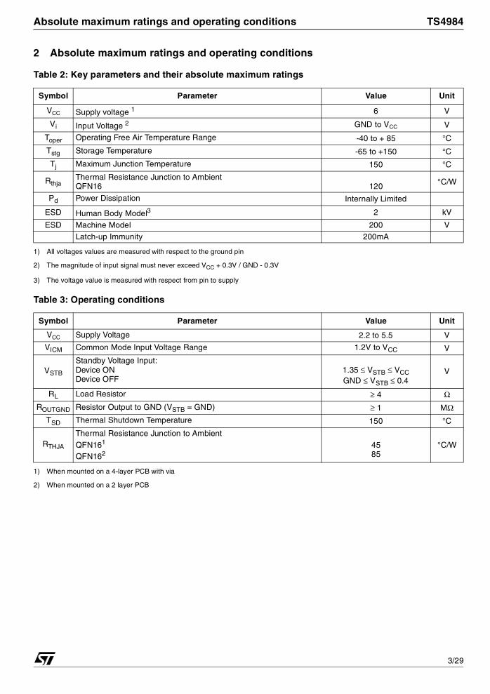
Absolute maximum ratings and operating conditions TS4984
2 Absolute maximum ratings and operating conditions
Table 2: Key parameters and their absolute maximum ratings
Symbol Parameter Value Unit
VCC Supply voltage 1
1) All voltages values are measured with respect to the ground pin
6 V
Vi Input Voltage 2
2) The magnitude of input signal must never exceed VCC + 0.3V / GND - 0.3V
GND to VCC V
Toper Operating Free Air Temperature Range -40 to + 85 °C
Tstg Storage Temperature -65 to +150 °C
Tj Maximum Junction Temperature 150 °C
RthjaThermal Resistance Junction to Ambient QFN16 120 °C/W
Pd Power Dissipation Internally Limited
ESD Human Body Model3
3) The voltage value is measured with respect from pin to supply
2 kV
ESD Machine Model 200 VLatch-up Immunity 200mA
Table 3: Operating conditions
Symbol Parameter Value Unit
VCC Supply Voltage 2.2 to 5.5 V
VICM Common Mode Input Voltage Range 1.2V to VCC V
VSTB
Standby Voltage Input: Device ONDevice OFF
1.35 ≤ VSTB ≤ VCCGND ≤ VSTB ≤ 0.4
V
RL Load Resistor ≥ 4 ΩROUTGND Resistor Output to GND (VSTB = GND) ≥ 1 MΩ
TSD Thermal Shutdown Temperature 150 °C
RTHJA
Thermal Resistance Junction to AmbientQFN161
QFN162
1) When mounted on a 4-layer PCB with via
2) When mounted on a 2 layer PCB
4585
°C/W
3/29
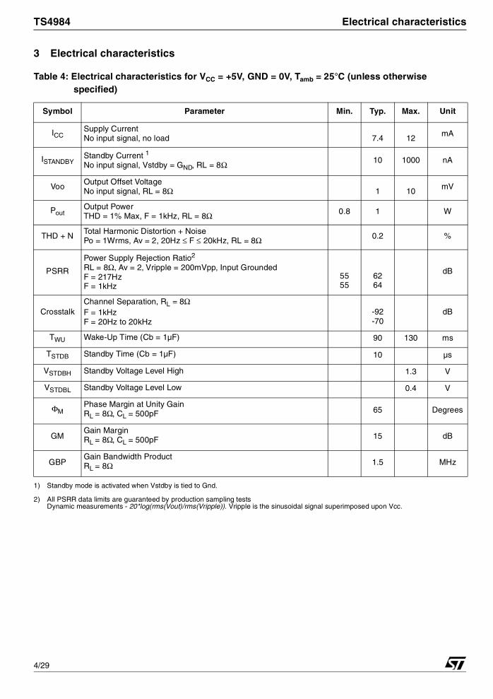
TS4984 Electrical characteristics
3 Electrical characteristics
Table 4: Electrical characteristics for VCC = +5V, GND = 0V, Tamb = 25°C (unless otherwise specified)
Symbol Parameter Min. Typ. Max. Unit
ICCSupply Current No input signal, no load 7.4 12
mA
ISTANDBYStandby Current 1
No input signal, Vstdby = GND, RL = 8Ω
1) Standby mode is activated when Vstdby is tied to Gnd.
10 1000 nA
VooOutput Offset VoltageNo input signal, RL = 8Ω 1 10
mV
PoutOutput PowerTHD = 1% Max, F = 1kHz, RL = 8Ω 0.8 1 W
THD + NTotal Harmonic Distortion + NoisePo = 1Wrms, Av = 2, 20Hz ≤ F ≤ 20kHz, RL = 8Ω 0.2 %
PSRR
Power Supply Rejection Ratio2
RL = 8Ω, Av = 2, Vripple = 200mVpp, Input GroundedF = 217HzF = 1kHz
2) All PSRR data limits are guaranteed by production sampling testsDynamic measurements - 20*log(rms(Vout)/rms(Vripple)). Vripple is the sinusoidal signal superimposed upon Vcc.
5555
6264
dB
CrosstalkChannel Separation, RL = 8Ω F = 1kHzF = 20Hz to 20kHz
-92-70
dB
TWU Wake-Up Time (Cb = 1µF) 90 130 ms
TSTDB Standby Time (Cb = 1µF) 10 µs
VSTDBH Standby Voltage Level High 1.3 V
VSTDBL Standby Voltage Level Low 0.4 V
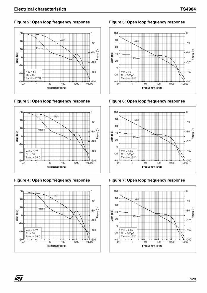
ΦMPhase Margin at Unity GainRL = 8Ω, CL = 500pF 65 Degrees
GMGain MarginRL = 8Ω, CL = 500pF 15 dB
GBPGain Bandwidth ProductRL = 8Ω 1.5 MHz
4/29
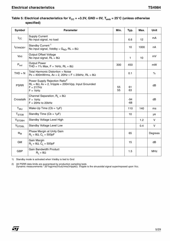
Electrical characteristics TS4984
Table 5: Electrical characteristics for VCC = +3.3V, GND = 0V, Tamb = 25°C (unless otherwise specified)
Symbol Parameter Min. Typ. Max. Unit
ICCSupply Current No input signal, no load 6.6 12
mA
ISTANDBYStandby Current 1
No input signal, Vstdby = GND, RL = 8Ω 10 1000 nA
VooOutput Offset VoltageNo input signal, RL = 8Ω 1 10
mV
PoutOutput PowerTHD = 1% Max, F = 1kHz, RL = 8Ω 300 450 mW
THD + NTotal Harmonic Distortion + NoisePo = 400mWrms, Av = 2, 20Hz ≤ F ≤ 20kHz, RL = 8Ω 0.1 %
PSRR
Power Supply Rejection Ratio2
RL = 8Ω, Av = 2, Vripple = 200mVpp, Input GroundedF = 217HzF = 1kHz
5555
6163
dB
CrosstalkChannel Separation, RL = 8Ω F = 1kHzF = 20Hz to 20kHz
-94-68
dB
TWU Wake-Up Time (Cb = 1µF) 110 140 ms
TSTDB Standby Time (Cb = 1µF) 10 µs
VSTDBH Standby Voltage Level High 1.2 V
VSTDBL Standby Voltage Level Low 0.4 V
ΦMPhase Margin at Unity GainRL = 8Ω, CL = 500pF 65 Degrees
GMGain MarginRL = 8Ω, CL = 500pF 15 dB
GBPGain Bandwidth Product RL = 8Ω 1.5 MHz
1) Standby mode is activated when Vstdby is tied to Gnd
2) All PSRR data limits are guaranteed by production sampling testsDynamic measurements - 20*log(rms(Vout)/rms(Vripple)). Vripple is the sinusoidal signal superimposed upon Vcc.
5/29
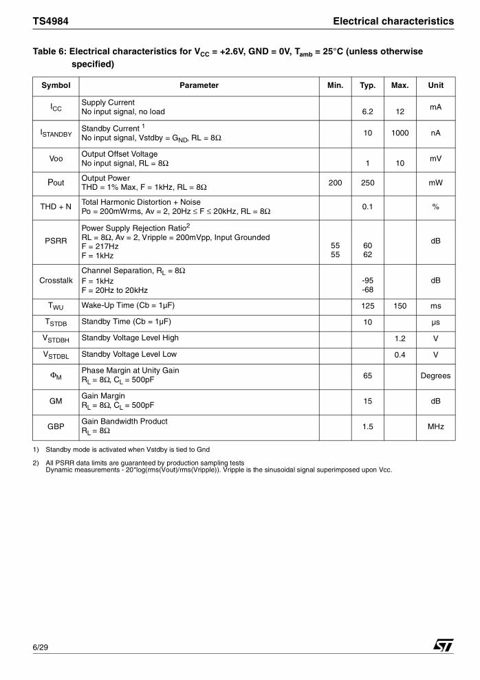
TS4984 Electrical characteristics
Table 6: Electrical characteristics for VCC = +2.6V, GND = 0V, Tamb = 25°C (unless otherwise specified)
Symbol Parameter Min. Typ. Max. Unit
ICCSupply Current No input signal, no load 6.2 12
mA
ISTANDBYStandby Current 1
No input signal, Vstdby = GND, RL = 8Ω 10 1000 nA
VooOutput Offset VoltageNo input signal, RL = 8Ω 1 10
mV
PoutOutput PowerTHD = 1% Max, F = 1kHz, RL = 8Ω 200 250 mW
THD + NTotal Harmonic Distortion + NoisePo = 200mWrms, Av = 2, 20Hz ≤ F ≤ 20kHz, RL = 8Ω 0.1 %
PSRR
Power Supply Rejection Ratio2
RL = 8Ω, Av = 2, Vripple = 200mVpp, Input GroundedF = 217HzF = 1kHz
5555
6062
dB
CrosstalkChannel Separation, RL = 8Ω F = 1kHzF = 20Hz to 20kHz
-95-68
dB
TWU Wake-Up Time (Cb = 1µF) 125 150 ms
TSTDB Standby Time (Cb = 1µF) 10 µs
VSTDBH Standby Voltage Level High 1.2 V
VSTDBL Standby Voltage Level Low 0.4 V
ΦMPhase Margin at Unity GainRL = 8Ω, CL = 500pF 65 Degrees
GMGain MarginRL = 8Ω, CL = 500pF 15 dB
GBPGain Bandwidth ProductRL = 8Ω 1.5 MHz
1) Standby mode is activated when Vstdby is tied to Gnd
2) All PSRR data limits are guaranteed by production sampling testsDynamic measurements - 20*log(rms(Vout)/rms(Vripple)). Vripple is the sinusoidal signal superimposed upon Vcc.
6/29
Electrical characteristics TS4984
Figure 2: Open loop frequency response
Figure 3: Open loop frequency response
Figure 4: Open loop frequency response
Figure 5: Open loop frequency response
Figure 6: Open loop frequency response
Figure 7: Open loop frequency response
0.1 1 10 100 1000 10000-60
-40
-20
0
20
40
60
-200
-160
-120
-80
-40
0
Gain
Phase
Gai
n (
dB
)
Frequency (kHz)
Vcc = 5VRL = 8ΩTamb = 25°C
Ph
ase
(°)
0.1 1 10 100 1000 10000-60
-40
-20
0
20
40
60
-200
-160
-120
-80
-40
0
Gain
Phase
Gai
n (
dB
)
Frequency (kHz)
Vcc = 3.3VRL = 8ΩTamb = 25°C
Ph
ase
(°)
0.1 1 10 100 1000 10000-60
-40
-20
0
20
40
60
-200
-160
-120
-80
-40
0
Gain
Phase
Gai
n (
dB
)
Frequency (kHz)
Vcc = 2.6VRL = 8ΩTamb = 25°C
Ph
ase
(°)
0.1 1 10 100 1000 10000-40
-20
0
20
40
60
80
100
-200
-160
-120
-80
-40
0
Gain
Phase
Gai
n (
dB
)
Frequency (kHz)
Vcc = 5VCL = 560pFTamb = 25°C
Ph
ase
(°)
0.1 1 10 100 1000 10000-40
-20
0
20
40
60
80
100
-200
-160
-120
-80
-40
0
Gain
Phase
Gai
n (
dB
)
Frequency (kHz)
Vcc = 3.3VCL = 560pFTamb = 25°C
Ph
ase
(°)
0.1 1 10 100 1000 10000-40
-20
0
20
40
60
80
100
-200
-160
-120
-80
-40
0
Gain
Phase
Gai
n (
dB
)
Frequency (kHz)
Vcc = 2.6VCL = 560pFTamb = 25°C
Ph
ase
(°)
7/29
TS4984 Electrical characteristics
Figure 8: Power supply rejection ratio (PSRR) vs. frequency
Figure 9: Power supply rejection ratio (PSRR) vs. frequency
Figure 10: Power supply rejection ratio (PSRR) vs. frequency
Figure 11: Power supply rejection ratio (PSRR) vs. frequency
Figure 12: Power supply rejection ratio (PSRR) vs. frequency
Figure 13: Power supply rejection ratio (PSRR) vs. frequency
100 1000 10000 100000-70
-60
-50
-40
-30
-20
-10
0
Vcc :2.2V2.6V3.3V5V
Vripple = 200mVppAv = 2 Input = GroundedCb = Cin = 1µFRL >= 4ΩTamb = 25°C
PS
RR
(d
B)
Frequency (Hz)
100 1000 10000 100000-60
-50
-40
-30
-20
-10
0
Vcc : 2.2V2.6V3.3V5V
Vripple = 200mVppAv = 5 Input = GroundedCb = Cin = 1µFRL >= 4ΩTamb = 25°C
PS
RR
(d
B)
Frequency (Hz)
100 1000 10000 100000
-50
-40
-30
-20
-10
0
Vcc : 2.2V2.6V3.3V5V
Vripple = 200mVppAv = 10 Input = GroundedCb = Cin = 1µFRL >= 4ΩTamb = 25°C
PS
RR
(d
B)
Frequency (Hz)
100 1000 10000 100000-60
-50
-40
-30
-20
-10
0
Vcc = 5, 3.3, 2.5 & 2.2V
Vripple = 200mVppAv = 2 Input = GroundedCb = 0.1µF, Cin = 1µFRL >= 4ΩTamb = 25°C
PS
RR
(d
B)
Frequency (Hz)
100 1000 10000 100000-80
-70
-60
-50
-40
-30
-20
-10
0
Vcc = 2.2, 2.6, 3.3, 5VVripple = 200mVppRfeed = 22kΩ Input = FloatingCb = 1µFRL >= 4ΩTamb = 25°C
PS
RR
(d
B)
Frequency (Hz)
100 1000 10000 100000-80
-70
-60
-50
-40
-30
-20
-10
0
Vcc = 2.2, 2.6, 3.3, 5VVripple = 200mVppRfeed = 22kΩ Input = FloatingCb = 0.1µFRL >= 4ΩTamb = 25°C
PS
RR
(d
B)
Frequency (Hz)
8/29
Electrical characteristics TS4984
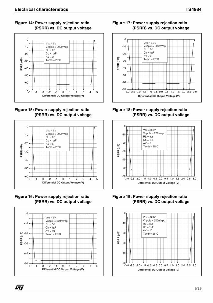
Figure 14: Power supply rejection ratio (PSRR) vs. DC output voltage
Figure 15: Power supply rejection ratio (PSRR) vs. DC output voltage
Figure 16: Power supply rejection ratio (PSRR) vs. DC output voltage
Figure 17: Power supply rejection ratio (PSRR) vs. DC output voltage
Figure 18: Power supply rejection ratio (PSRR) vs. DC output voltage
Figure 19: Power supply rejection ratio (PSRR) vs. DC output voltage
-5 -4 -3 -2 -1 0 1 2 3 4 5-70
-60
-50
-40
-30
-20
-10
0
Vcc = 5VVripple = 200mVppRL = 8ΩCb = 1µFAV = 2Tamb = 25°C
PS
RR
(d
B)
Differential DC Output Voltage (V)
-5 -4 -3 -2 -1 0 1 2 3 4 5-60
-50
-40
-30
-20
-10
0
Vcc = 5VVripple = 200mVppRL = 8ΩCb = 1µFAV = 5Tamb = 25°C
PS
RR
(d
B)
Differential DC Output Voltage (V)
-5 -4 -3 -2 -1 0 1 2 3 4 5-50
-40
-30
-20
-10
0
Vcc = 5VVripple = 200mVppRL = 8ΩCb = 1µFAV = 10Tamb = 25°C
PS
RR
(d
B)
Differential DC Output Voltage (V)
-3.0 -2.5 -2.0 -1.5 -1.0 -0.5 0.0 0.5 1.0 1.5 2.0 2.5 3.0-70
-60
-50
-40
-30
-20
-10
0Vcc = 3.3VVripple = 200mVppRL = 8ΩCb = 1µFAV = 2Tamb = 25°C
PS
RR
(d
B)
Differential DC Output Voltage (V)
-3.0 -2.5 -2.0 -1.5 -1.0 -0.5 0.0 0.5 1.0 1.5 2.0 2.5 3.0-60
-50
-40
-30
-20
-10
0
Vcc = 3.3VVripple = 200mVppRL = 8ΩCb = 1µFAV = 5Tamb = 25°C
PS
RR
(d
B)
Differential DC Output Voltage (V)
-3.0 -2.5 -2.0 -1.5 -1.0 -0.5 0.0 0.5 1.0 1.5 2.0 2.5 3.0-50
-40
-30
-20
-10
0
Vcc = 3.3VVripple = 200mVppRL = 8ΩCb = 1µFAV = 10Tamb = 25°C
PS
RR
(d
B)
Differential DC Output Voltage (V)
9/29
TS4984 Electrical characteristics
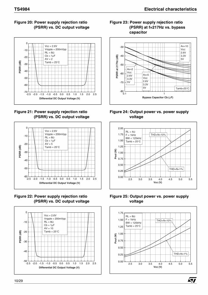
Figure 20: Power supply rejection ratio (PSRR) vs. DC output voltage
Figure 21: Power supply rejection ratio (PSRR) vs. DC output voltage
Figure 22: Power supply rejection ratio (PSRR) vs. DC output voltage
Figure 23: Power supply rejection ratio (PSRR) at f=217Hz vs. bypass capacitor
Figure 24: Output power vs. power supply voltage
Figure 25: Output power vs. power supply voltage
-2.5 -2.0 -1.5 -1.0 -0.5 0.0 0.5 1.0 1.5 2.0 2.5-70
-60
-50
-40
-30
-20
-10
0Vcc = 2.6VVripple = 200mVppRL = 8ΩCb = 1µFAV = 2Tamb = 25°C
PS
RR
(d
B)
Differential DC Output Voltage (V)
-2.5 -2.0 -1.5 -1.0 -0.5 0.0 0.5 1.0 1.5 2.0 2.5-60
-50
-40
-30
-20
-10
0Vcc = 2.6VVripple = 200mVppRL = 8ΩCb = 1µFAV = 5Tamb = 25°C
PS
RR
(d
B)
Differential DC Output Voltage (V)
-2.5 -2.0 -1.5 -1.0 -0.5 0.0 0.5 1.0 1.5 2.0 2.5-50
-40
-30
-20
-10
0Vcc = 2.6VVripple = 200mVppRL = 8ΩCb = 1µFAV = 10Tamb = 25°C
PS
RR
(d
B)
Differential DC Output Voltage (V)
0.1 1-80
-70
-60
-50
-40
-30 Av=10 Vcc:2.6V3.3V5V
Av=5 Vcc:2.6V3.3V5V
Av=2 Vcc:2.6V3.3V5V
Tamb=25°C
PS
RR
at
217H
z (d
B)
Bypass Capacitor Cb ( F)
2.5 3.0 3.5 4.0 4.5 5.0 5.50.00
0.25
0.50
0.75
1.00
1.25
1.50
1.75
2.00
THD+N=10%
THD+N=1%
RL = 4ΩF = 1kHzBW < 125kHzTamb = 25°C
Po
ut
(W)
Vcc (V)
2.5 3.0 3.5 4.0 4.5 5.0 5.50.00
0.25
0.50
0.75
1.00
1.25
1.50
1.75
THD+N=10%
THD+N=1%
RL = 8ΩF = 1kHzBW < 125kHzTamb = 25°C
Po
ut
(W)
Vcc (V)
10/29
Electrical characteristics TS4984
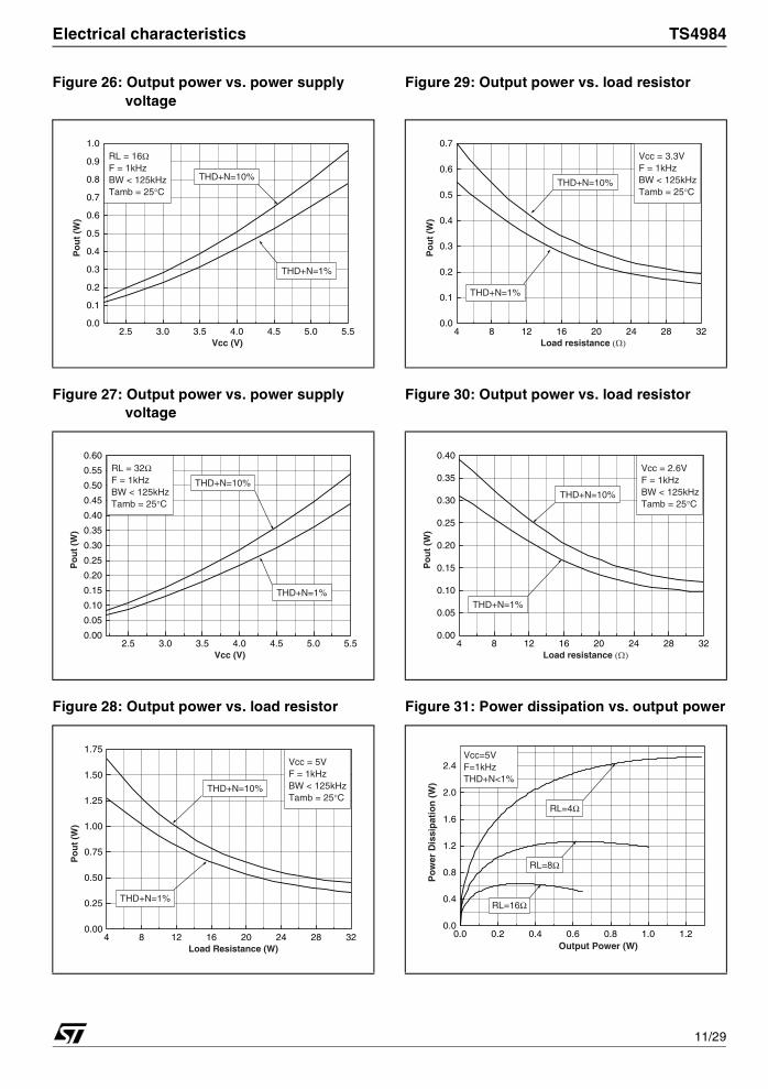
Figure 26: Output power vs. power supply voltage
Figure 27: Output power vs. power supply voltage
Figure 28: Output power vs. load resistor
Figure 29: Output power vs. load resistor
Figure 30: Output power vs. load resistor
Figure 31: Power dissipation vs. output power
2.5 3.0 3.5 4.0 4.5 5.0 5.50.0
0.1
0.2
0.3
0.4
0.5
0.6
0.7
0.8
0.9
1.0
THD+N=10%
THD+N=1%
RL = 16ΩF = 1kHzBW < 125kHzTamb = 25°C
Po
ut
(W)
Vcc (V)
2.5 3.0 3.5 4.0 4.5 5.0 5.50.00
0.05
0.10
0.15
0.20
0.25
0.30
0.35
0.40
0.45
0.50
0.55
0.60
THD+N=10%
THD+N=1%
RL = 32ΩF = 1kHzBW < 125kHzTamb = 25°C
Po
ut
(W)
Vcc (V)
4 8 12 16 20 24 28 320.00
0.25
0.50
0.75
1.00
1.25
1.50
1.75
THD+N=10%
THD+N=1%
Vcc = 5VF = 1kHzBW < 125kHzTamb = 25°C
Po
ut
(W)
Load Resistance (W)
4 8 12 16 20 24 28 320.0
0.1
0.2
0.3
0.4
0.5
0.6
0.7
THD+N=10%
THD+N=1%
Vcc = 3.3VF = 1kHzBW < 125kHzTamb = 25°C
Po
ut
(W)
Load resistance
4 8 12 16 20 24 28 320.00
0.05
0.10
0.15
0.20
0.25
0.30
0.35
0.40
THD+N=10%
THD+N=1%
Vcc = 2.6VF = 1kHzBW < 125kHzTamb = 25°C
Po
ut
(W)
Load resistance
0.0 0.2 0.4 0.6 0.8 1.0 1.20.0
0.4
0.8
1.2
1.6
2.0
2.4
RL=16Ω
RL=8Ω
Vcc=5VF=1kHzTHD+N<1%
RL=4Ω
Po
wer
Dis
sip
atio
n (
W)
Output Power (W)
11/29
TS4984 Electrical characteristics
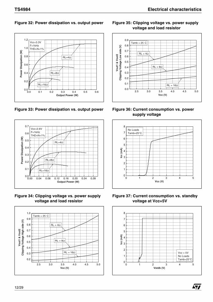
Figure 32: Power dissipation vs. output power
Figure 33: Power dissipation vs. output power
Figure 34: Clipping voltage vs. power supply voltage and load resistor
Figure 35: Clipping voltage vs. power supply voltage and load resistor
Figure 36: Current consumption vs. power supply voltage
Figure 37: Current consumption vs. standby voltage at Vcc=5V
0.0 0.1 0.2 0.3 0.4 0.5 0.60.0
0.2
0.4
0.6
0.8
1.0
1.2
RL=16Ω
RL=8Ω
Vcc=3.3VF=1kHzTHD+N<1%
RL=4Ω
Po
wer
Dis
sip
atio
n (
W)
Output Power (W)
0.00 0.04 0.08 0.12 0.16 0.20 0.24 0.280.0
0.1
0.2
0.3
0.4
0.5
0.6
0.7
RL=16Ω
RL=8Ω
Vcc=2.6VF=1kHzTHD+N<1%
RL=4Ω
Po
wer
Dis
sip
atio
n (
W)
Output Power (W)
2.5 3.0 3.5 4.0 4.5 5.0
0.2
0.3
0.4
0.5
0.6
0.7
0.8
0.9
1.0
RL = 16Ω
RL = 8Ω
RL = 4Ω
Tamb = 25 C
Vo
ut1
& V
ou
t2C
lipp
ing
Vo
ltag
e H
igh
sid
e (V
)
Vcc (V)
2.5 3.0 3.5 4.0 4.5 5.00.0
0.1
0.2
0.3
0.4
0.5
0.6
0.7
0.8
0.9
RL = 16Ω
RL = 8Ω
RL = 4Ω
Tamb = 25 C
Vo
ut1
& V
ou
t2C
lipp
ing
Vo
ltag
e L
ow
sid
e (V
)
Vcc (V)
No LoadsTamb=25°C
Vcc = 5VNo LoadsTamb=25°C
12/29
Electrical characteristics TS4984
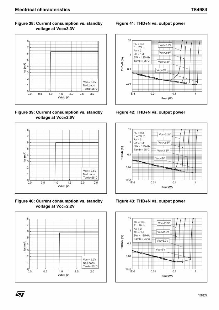
Figure 38: Current consumption vs. standby voltage at Vcc=3.3V
Figure 39: Current consumption vs. standby voltage at Vcc=2.6V
Figure 40: Current consumption vs. standby voltage at Vcc=2.2V
Figure 41: THD+N vs. output power
Figure 42: THD+N vs. output power
Figure 43: THD+N vs. output power
Vcc = 3.3VNo LoadsTamb=25°C
Vcc = 2.6VNo LoadsTamb=25°C
Vcc = 2.2VNo LoadsTamb=25°C
1E−3 0.01 0.1 1
0.01
0.1
1
10
Vcc=5V
Vcc=3.3V
Vcc=2.6V
Vcc=2.2VRL = 4ΩF = 20HzAv = 2Cb = 1µFBW < 125kHzTamb = 25°C
TH
D+N
(%
)
Pout (W)
1E−3 0.01 0.1 11E−3
0.01
0.1
1
10
Vcc=5V
Vcc=3.3V
Vcc=2.6V
Vcc=2.2VRL = 8ΩF = 20HzAv = 2Cb = 1µFBW < 125kHzTamb = 25°C
TH
D+N
(%
)
Pout (W)
1E−3 0.01 0.1 11E−3
0.01
0.1
1
10
Vcc=2.6V
Vcc=3.3V
Vcc=5V
Vcc=2.2VRL = 16ΩF = 20HzAv = 2Cb = 1µFBW < 125kHzTamb = 25°C
TH
D+N
(%
)
Pout (W)
13/29
TS4984 Electrical characteristics
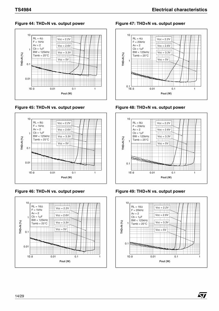
Figure 44: THD+N vs. output power
Figure 45: THD+N vs. output power
Figure 46: THD+N vs. output power
Figure 47: THD+N vs. output power
Figure 48: THD+N vs. output power
Figure 49: THD+N vs. output power
1E−3 0.01 0.1 1
0.01
0.1
1
10
Vcc = 3.3V
Vcc = 5V
Vcc = 2.6V
Vcc = 2.2VRL = 4ΩF = 1kHzAv = 2Cb = 1µFBW < 125kHzTamb = 25°C
TH
D+N
(%
)
Pout (W)
1E−3 0.01 0.1 1
0.01
0.1
1
10
Vcc = 3.3V
Vcc = 5V
Vcc = 2.6V
Vcc = 2.2VRL = 8ΩF = 1kHzAv = 2Cb = 1µFBW < 125kHzTamb = 25°C
TH
D+N
(%
)
Pout (W)
1E−3 0.01 0.1 1
0.01
0.1
1
10
Vcc = 5V
Vcc = 3.3V
Vcc = 2.6V
Vcc = 2.2VRL = 16ΩF = 1kHzAv = 2Cb = 1µFBW < 125kHzTamb = 25°C
TH
D+N
(%
)
Pout (W)
1E−3 0.01 0.1 10.1
1
10
Vcc = 3.3V
Vcc = 5V
Vcc = 2.6V
Vcc = 2.2VRL = 4ΩF = 20kHzAv = 2Cb = 1µFBW < 125kHzTamb = 25°C
TH
D+N
(%
)
Pout (W)
1E−3 0.01 0.1 1
0.1
1
10
Vcc = 3.3V
Vcc = 5V
Vcc = 2.6V
Vcc = 2.2VRL = 8ΩF = 20kHzAv = 2Cb = 1µFBW < 125kHzTamb = 25°C
TH
D+N
(%
)
Pout (W)
1E−3 0.01 0.1 1
0.1
1
10
Vcc = 5V
Vcc = 3.3V
Vcc = 2.6V
Vcc = 2.2VRL = 16ΩF = 20kHzAv = 2Cb = 1µFBW < 125kHzTamb = 25°C
TH
D+N
(%
)
Pout (W)
14/29
Electrical characteristics TS4984
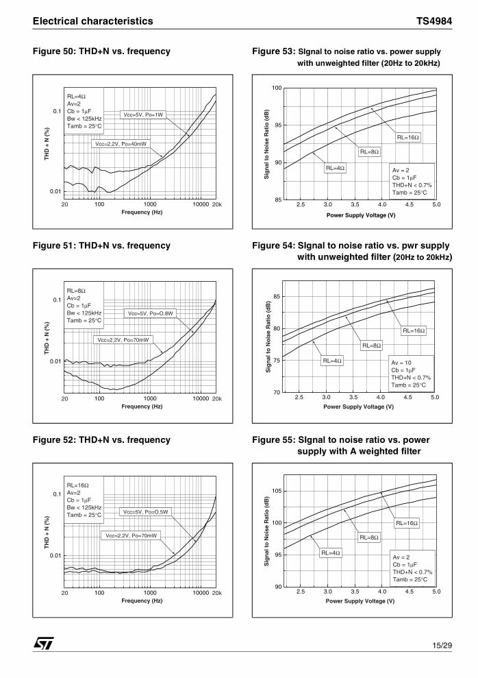
Figure 50: THD+N vs. frequency
Figure 51: THD+N vs. frequency
Figure 52: THD+N vs. frequency
Figure 53: SIgnal to noise ratio vs. power supply with unweighted filter (20Hz to 20kHz)
Figure 54: SIgnal to noise ratio vs. pwr supply with unweighted filter (20Hz to 20kHz)
Figure 55: SIgnal to noise ratio vs. power supply with A weighted filter
100 1000 10000
0.01
0.1
Vcc=2.2V, Po=40mW
Vcc=5V, Po=1W
RL=4ΩAv=2Cb = 1µFBw < 125kHzTamb = 25°C
20k20
TH
D +
N (
%)
Frequency (Hz)
100 1000 10000
0.01
0.1
Vcc=2.2V, Po=70mW
Vcc=5V, Po=O.8W
RL=8ΩAv=2Cb = 1µFBw < 125kHzTamb = 25°C
20k20
TH
D +
N (
%)
Frequency (Hz)
100 1000 10000
0.01
0.1
Vcc=2.2V, Po=70mW
Vcc=5V, Po=O.5W
RL=16ΩAv=2Cb = 1µFBw < 125kHzTamb = 25°C
20k20
TH
D +
N (
%)
Frequency (Hz)
2.5 3.0 3.5 4.0 4.5 5.085
90
95
100
Power Supply Voltage (V)
Av = 2Cb = 1µFTHD+N < 0.7%Tamb = 25°C
RL=16Ω
RL=4Ω
RL=8Ω
Sig
nal
to
No
ise
Rat
io (
dB
)
2.5 3.0 3.5 4.0 4.5 5.070
75
80
85
RL=16Ω
Av = 10Cb = 1µFTHD+N < 0.7%Tamb = 25°C
RL=4Ω
RL=8Ω
Sig
nal
to
No
ise
Rat
io (
dB
)
Power Supply Voltage (V)
2.5 3.0 3.5 4.0 4.5 5.090
95
100
105
RL=8Ω
RL=16Ω
Av = 2Cb = 1µFTHD+N < 0.7%Tamb = 25°C
RL=4Ω
Sig
nal
to
No
ise
Rat
io (
dB
)
Power Supply Voltage (V)
15/29
TS4984 Electrical characteristics
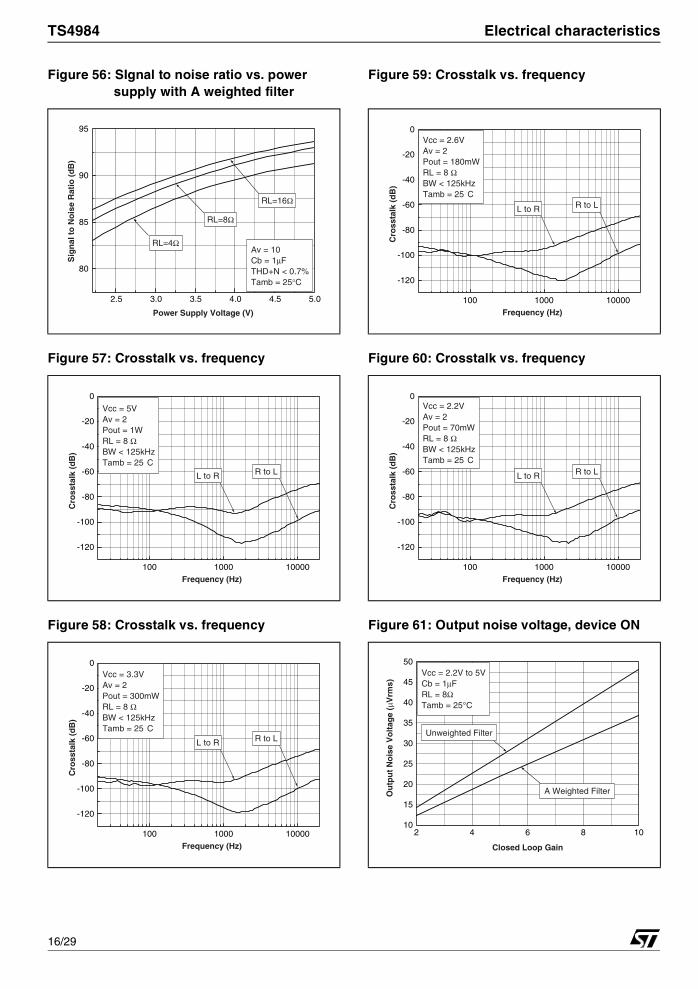
Figure 56: SIgnal to noise ratio vs. power supply with A weighted filter
Figure 57: Crosstalk vs. frequency
Figure 58: Crosstalk vs. frequency
Figure 59: Crosstalk vs. frequency
Figure 60: Crosstalk vs. frequency
Figure 61: Output noise voltage, device ON
2.5 3.0 3.5 4.0 4.5 5.0
80
85
90
95
RL=16Ω
RL=8Ω
RL=4ΩAv = 10Cb = 1µFTHD+N < 0.7%Tamb = 25°C
Sig
nal
to
No
ise
Rat
io (
dB
)
Power Supply Voltage (V)
100 1000 10000
-120
-100
-80
-60
-40
-20
0
Vcc = 5VAv = 2Pout = 1WRL = 8 ΩBW < 125kHzTamb = 25 C
L to R R to L
Cro
ssta
lk (
dB
)
Frequency (Hz)
100 1000 10000
-120
-100
-80
-60
-40
-20
0Vcc = 3.3VAv = 2Pout = 300mWRL = 8 ΩBW < 125kHzTamb = 25 C
L to R R to L
Cro
ssta
lk (
dB
)
Frequency (Hz)
100 1000 10000
-120
-100
-80
-60
-40
-20
0Vcc = 2.6VAv = 2Pout = 180mWRL = 8 ΩBW < 125kHzTamb = 25 C
L to R R to L
Cro
ssta
lk (
dB
)
Frequency (Hz)
100 1000 10000
-120
-100
-80
-60
-40
-20
0Vcc = 2.2VAv = 2Pout = 70mWRL = 8 ΩBW < 125kHzTamb = 25 C
L to R R to L
Cro
ssta
lk (
dB
)
Frequency (Hz)
2 4 6 8 1010
15
20
25
30
35
40
45
50
A Weighted Filter
Unweighted Filter
Vcc = 2.2V to 5VCb = 1µFRL = 8ΩTamb = 25°C
Ou
tpu
t N
ois
e V
olt
age
(V
rms)
Closed Loop Gain
16/29
Electrical characteristics TS4984
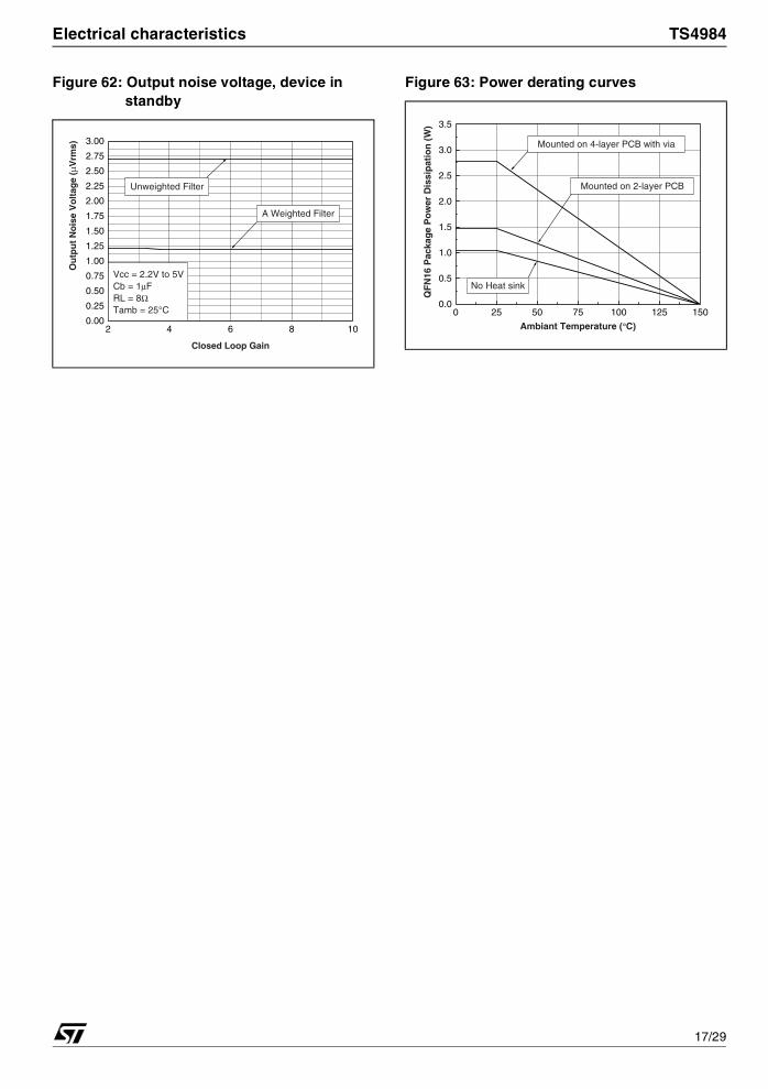
Figure 62: Output noise voltage, device in standby
Figure 63: Power derating curves
2 4 6 8 100.00
0.25
0.50
0.75
1.00
1.25
1.50
1.75
2.00
2.25
2.50
2.75
3.00
A Weighted Filter
Unweighted Filter
Vcc = 2.2V to 5VCb = 1µFRL = 8ΩTamb = 25°C
Ou
tpu
t N
ois
e V
olt
age
(V
rms)
Closed Loop Gain
0 25 50 75 100 125 1500.0
0.5
1.0
1.5
2.0
2.5
3.0
3.5
Mounted on 2-layer PCB
No Heat sink
Mounted on 4-layer PCB with via
QF
N16
Pac
kag
e P
ow
er D
issi
pat
ion
(W
)
Ambiant Temperature ( C)
17/29
TS4984 Application Information
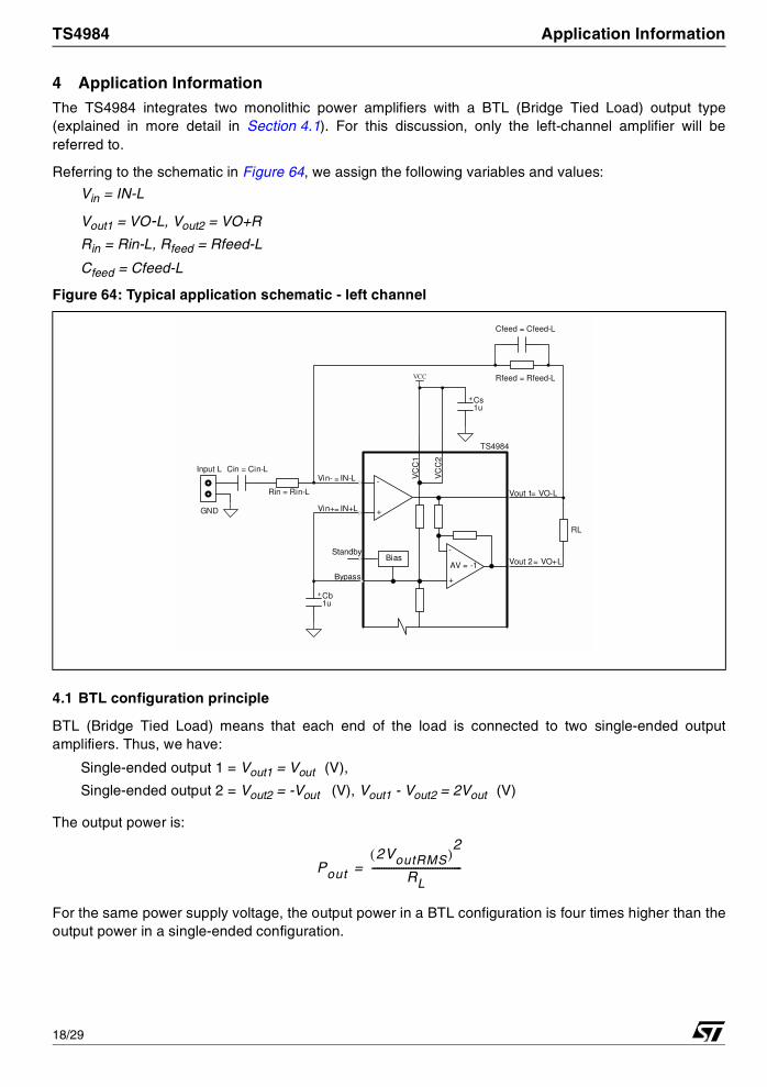
4 Application Information
The TS4984 integrates two monolithic power amplifiers with a BTL (Bridge Tied Load) output type(explained in more detail in Section 4.1). For this discussion, only the left-channel amplifier will bereferred to.
Referring to the schematic in Figure 64, we assign the following variables and values:
Vin = IN-L
Vout1 = VO-L, Vout2 = VO+R
Rin = Rin-L, Rfeed = Rfeed-L
Cfeed = Cfeed-L
4.1 BTL configuration principle
BTL (Bridge Tied Load) means that each end of the load is connected to two single-ended outputamplifiers. Thus, we have:
Single-ended output 1 = Vout1 = Vout (V),
Single-ended output 2 = Vout2 = -Vout (V), Vout1 - Vout2 = 2Vout (V)
The output power is:
For the same power supply voltage, the output power in a BTL configuration is four times higher than theoutput power in a single-ended configuration.
Figure 64: Typical application schematic - left channel
Rin = Rin-L
Cin = Cin-LInput L
GND
Rfeed = Rfeed-LVCC
+ Cs1u
RL
Cfeed = Cfeed-L
AV = -1
Vin-
Vin+
Vout 1
Vout 2
+
-
+
-
VC
C1
VC
C2
VO-L
VO+L
IN-L
IN+L
=
=
=
=
Bias
Bypass
Standby
TS4984
+ Cb1u
Pout
2VoutRMS( )2
RL-------------------------------------=
18/29
Application Information TS4984
4.2 Gain in typical application schematic
The typical application schematic (Figure 64) is shown on page 18.
In the flat region (no Cin effect), the output voltage of the first stage is:
For the second stage: Vout2 = -Vout1 (V)
The differential output voltage is:
The differential gain, referred to as Gv for greater convenience, is:
Vout2 is in phase with Vin and Vout1 is phased 180° with Vin. This means that the positive terminal of theloudspeaker should be connected to Vout2 and the negative to Vout1.
4.3 Low and high frequency response
In the low frequency region, Cin starts to have an effect. Cin forms with Rin a high-pass filter with a -3dBcut-off frequency:
In the high frequency region, you can limit the bandwidth by adding a capacitor (Cfeed) in parallel withRfeed. It forms a low-pass filter with a -3dB cut-off frequency. FCH is in Hz.
Vout1 V– in( )Rfeed
Rin--------------- (V)=
Vout2 Vout1– 2Vin
RfeedRin
--------------- (V)=
Gv
Vout2 Vout1–
Vin------------------------------------ 2
RfeedRin
---------------= =
FCL1
2πRinCin-------------------------- (Hz)=
FCH1
2πRfeedCfeed---------------------------------------- (Hz)=
19/29
TS4984 Application Information
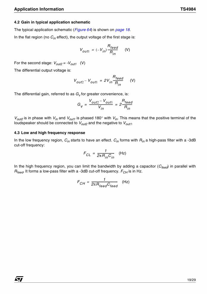
The following graph (Figure 65) shows an example of Cin and Cfeed influence.
4.4 Power dissipation and efficiency
Hypotheses:
Voltage and current in the load are sinusoidal (Vout and Iout).
Supply voltage is a pure DC source (Vcc).
Regarding the load we have:
and
and
Therefore, the average current delivered by the supply voltage is:
The power delivered by the supply voltage is:
Figure 65: Frequency response gain versus Cin & Cfeed
10 100 1000 10000-25
-20
-15
-10
-5
0
5
10
Rin = Rfeed = 22kΩTamb = 25°C
Cfeed = 2.2nF
Cfeed = 680pF
Cfeed = 330pF
Cin = 470nF
Cin = 82nF
Cin = 22nF
Gai
n (
dB
)
Frequency (Hz)
Vout = VPEAK sinωt (V)
Iout = Vout
RL-------------- (A)
Pout = VPEAK
2
2RL------------------------- (W)
ICCAVG = 2
VPEAK
πRL------------------- (A)
Psupply VCC ICCAVG⋅= W( )
20/29
Application Information TS4984
Then, the power dissipated by each amplifier is:
and the maximum value is obtained when:
and its value is:
Note: This maximum value is only depending on power supply voltage and load values.
The efficiency, η, is the ratio between the output power and the power supply:
The maximum theoretical value is reached when VPEAK = VCC, so that:
The TS4984 has two independent power amplifiers, and each amplifier produces heat due to its powerdissipation. Therefore, the maximum die temperature is the sum of the each amplifier’s maximum powerdissipation. It is calculated as follows:
Pdiss L = Power dissipation due to the left channel power amplifier.
Pdiss R = Power dissipation due to the right channel power amplifier.
Total Pdiss = Pdiss L + Pdiss R (W)
In most cases, Pdiss L = Pdiss R, giving:
or, stated differently:
Pdiss Psupply Pout–= W( )
Pdiss
2 2VCC
π RL
------------------------ Pout Pout–⋅= W( )
∂Pdiss
∂Pout--------------------- = 0
Pdissmax2Vcc
2
π2RL
-------------= W( )
η = Pout
Psupply--------------------- =
πVPEAK4VCC
-------------------------
π 4----- = 78.5%
Total Pdiss 2PdissL (W)=
Total Pdiss
4 2VCC
π RL
------------------------ Pout 2Pout–= W( )
21/29
TS4984 Application Information
4.5 Decoupling the circuit
Two capacitors are needed to correctly bypass the TS4984. A power supply bypass capacitor CS and abias voltage bypass capacitor CB.
CS has particular influence on the THD+N in the high frequency region (above 7 kHz) and an indirectinfluence on power supply disturbances. With a value for CS of 1 µF, you can expect similar THD+Nperformances to those shown in the datasheet. For example:
In the high frequency region, if CS is lower than 1 µF, it increases THD+N and disturbances on thepower supply rail are less filtered.
On the other hand, if CS is higher than 1 µF, those disturbances on the power supply rail are more
filtered.
Cb has an influence on THD+N at lower frequencies, but its function is critical to the final result of PSRR(with input grounded and in the lower frequency region), in the following manner:
If Cb is lower than 1µF, THD+N increases at lower frequencies and PSRR worsens.
If Cb is higher than 1µF, the benefit on THD+N at lower frequencies is small, but the benefit to PSRR
is substantial.
Note that Cin has a non-negligible effect on PSRR at lower frequencies. The lower the value of Cin, thehigher the PSRR.
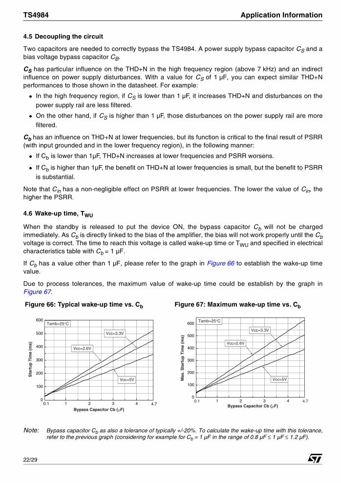
4.6 Wake-up time, TWU
When the standby is released to put the device ON, the bypass capacitor Cb will not be chargedimmediately. As Cb is directly linked to the bias of the amplifier, the bias will not work properly until the Cbvoltage is correct. The time to reach this voltage is called wake-up time or TWU and specified in electricalcharacteristics table with Cb = 1 µF.
If Cb has a value other than 1 µF, please refer to the graph in Figure 66 to establish the wake-up timevalue.
Due to process tolerances, the maximum value of wake-up time could be establish by the graph inFigure 67.
Note: Bypass capacitor Cb as also a tolerance of typically +/-20%. To calculate the wake-up time with this tolerance,refer to the previous graph (considering for example for Cb = 1 µF in the range of 0.8 µF ≤ 1 µF ≤ 1.2 µF).
Figure 66: Typical wake-up time vs. Cb Figure 67: Maximum wake-up time vs. Cb
1 2 3 40
100
200
300
400
500
600
4.70.1
Tamb=25°C
Vcc=2.6V
Vcc=3.3V
Vcc=5V
Sta
rtu
p T
ime
(ms)
Bypass Capacitor Cb ( F)
1 2 3 40
100
200
300
400
500
600Tamb=25°C
4.70.1
Vcc=5V
Vcc=3.3V
Vcc=2.6V
Max
. Sta
rtu
p T
ime
(ms)
Bypass Capacitor Cb ( F)
22/29
Application Information TS4984
4.7 Shutdown time
When the standby command is set, the time required to put the two output stages in high impedance andthe internal circuitry in shutdown mode is a few microseconds.
Note: In shutdown mode, Bypass pin and Vin- pin are short-circuited to ground by internal switches. This allows forthe quick discharge of the Cb and Cin capacitors.
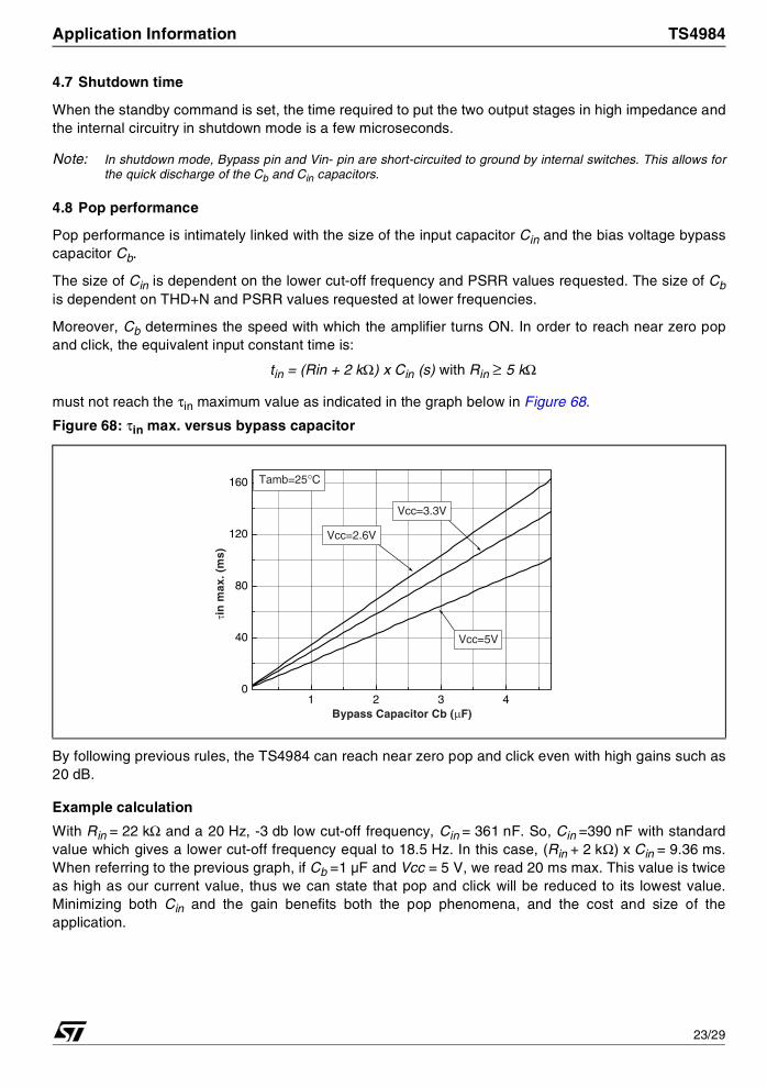
4.8 Pop performance
Pop performance is intimately linked with the size of the input capacitor Cin and the bias voltage bypasscapacitor Cb.
The size of Cin is dependent on the lower cut-off frequency and PSRR values requested. The size of Cbis dependent on THD+N and PSRR values requested at lower frequencies.
Moreover, Cb determines the speed with which the amplifier turns ON. In order to reach near zero popand click, the equivalent input constant time is:
tin = (Rin + 2 kΩ) x Cin (s) with Rin ≥ 5 kΩ
must not reach the τin maximum value as indicated in the graph below in Figure 68.
By following previous rules, the TS4984 can reach near zero pop and click even with high gains such as20 dB.
Example calculation
With Rin = 22 kΩ and a 20 Hz, -3 db low cut-off frequency, Cin = 361 nF. So, Cin =390 nF with standardvalue which gives a lower cut-off frequency equal to 18.5 Hz. In this case, (Rin + 2 kΩ) x Cin = 9.36 ms.When referring to the previous graph, if Cb =1 µF and Vcc = 5 V, we read 20 ms max. This value is twiceas high as our current value, thus we can state that pop and click will be reduced to its lowest value.Minimizing both Cin and the gain benefits both the pop phenomena, and the cost and size of theapplication.
Figure 68: τin max. versus bypass capacitor
1 2 3 40
40
80
120
160
Vcc=5V
Vcc=3.3V
Vcc=2.6V
Tamb=25°C
in m
ax. (
ms)
Bypass Capacitor Cb ( F)
23/29
TS4984 Application Information
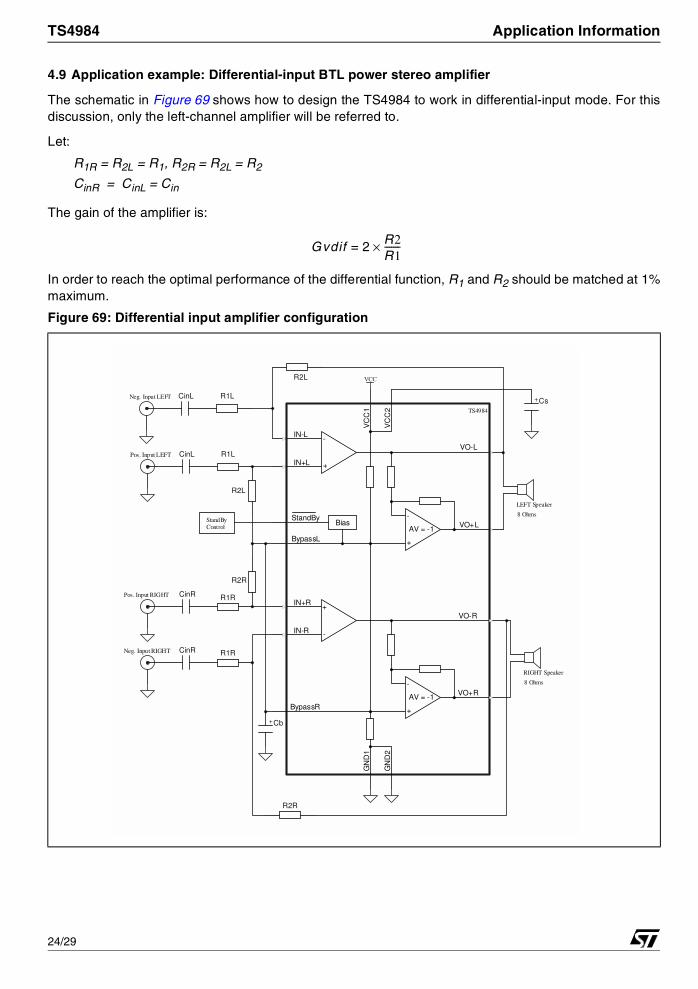
4.9 Application example: Differential-input BTL power stereo amplifier
The schematic in Figure 69 shows how to design the TS4984 to work in differential-input mode. For thisdiscussion, only the left-channel amplifier will be referred to.
Let:
R1R = R2L = R1, R2R = R2L = R2
CinR = CinL = Cin
The gain of the amplifier is:
In order to reach the optimal performance of the differential function, R1 and R2 should be matched at 1%maximum.
Figure 69: Differential input amplifier configuration
Gvdif = 2 R2R1-------×
R1LCinL
R2L VCC
+ Cs
+ Cb
Neg. Input LEFT
8 Ohms
LEFT Speaker
8 Ohms
RIGHT Speaker
R1RCinR
R2R
Neg. Input RIGHT
StandByControl
R1LCinLPos. Input LEFT
R1RCinRPos. Input RIGHT
R2L
R2R
BiasStandBy
VC
C1
GN
D1
BypassL
GN
D2
VC
C2
VO-L
VO+L
VO-R
VO+R
IN-L
IN+L
IN+R
IN-R
+
-
+
-
+
-
AV = -1
+
-
AV = -1BypassR
TS4984
24/29
Application Information TS4984
The value of the input capacitor CIN can be calculated with the following formula, using the -3dB lowerfrequency required (where FL is the lower frequency required):
Note: This formula is true only if:
is 5 times lower than FL.
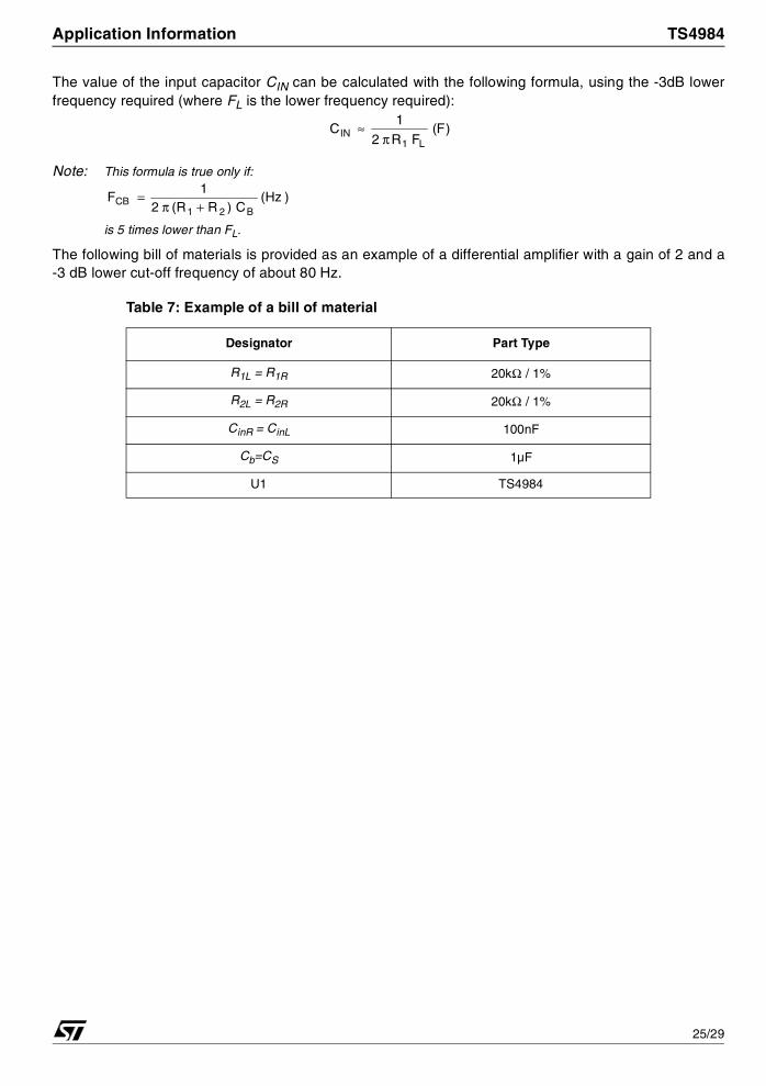
The following bill of materials is provided as an example of a differential amplifier with a gain of 2 and a-3 dB lower cut-off frequency of about 80 Hz.
Table 7: Example of a bill of material
Designator Part Type
R1L = R1R 20kΩ / 1%
R2L = R2R 20kΩ / 1%
CinR = CinL 100nF
Cb=CS 1µF
U1 TS4984
)F(FR2
1C
L1IN π
≈
)Hz(C)RR(2
1F
B21CB +π
=
25/29
TS4984 Application Information
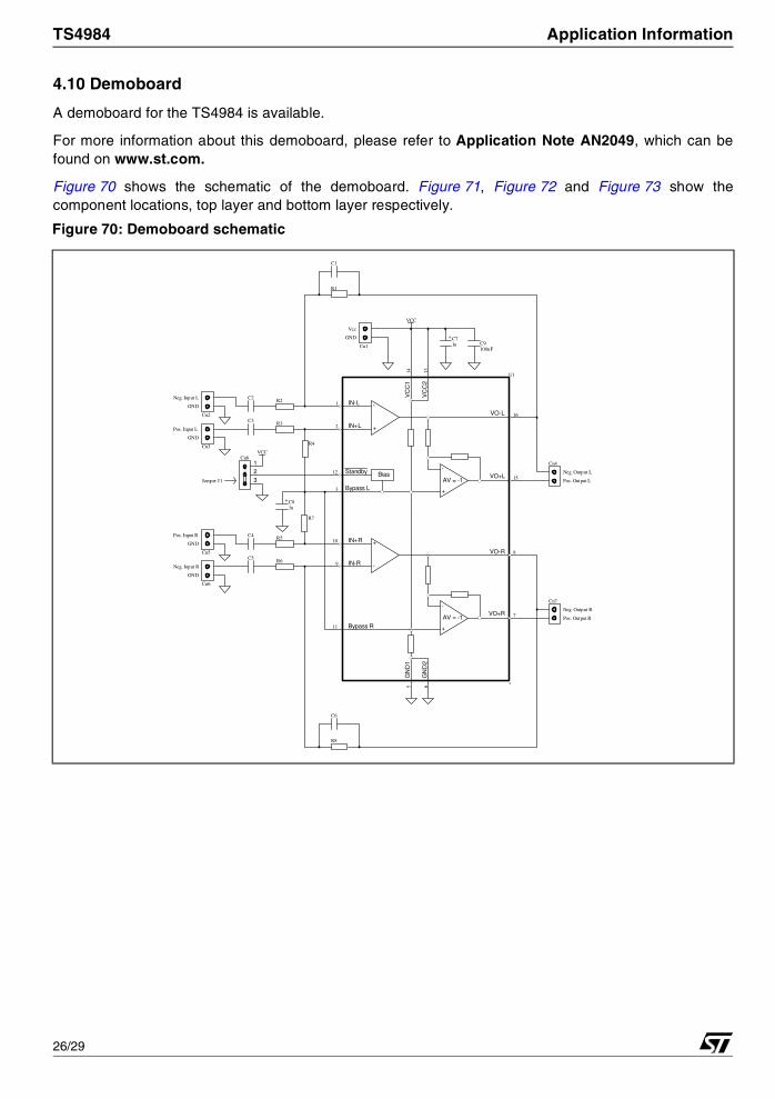
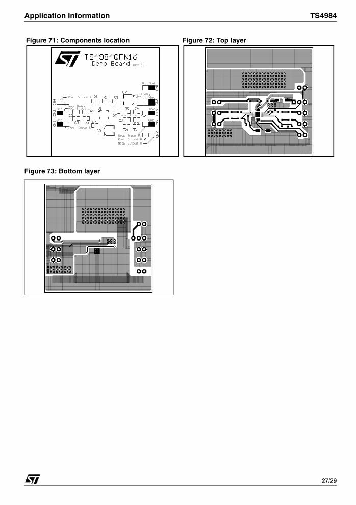
4.10 Demoboard
A demoboard for the TS4984 is available.
For more information about this demoboard, please refer to Application Note AN2049, which can befound on www.st.com.
Figure 70 shows the schematic of the demoboard. Figure 71, Figure 72 and Figure 73 show thecomponent locations, top layer and bottom layer respectively.
Figure 70: Demoboard schematic
1
2
12
145
16
15Bias
3
AV = -1Bypass L
Standby
VC
C1
+
-
+
-
AV = -1
GN
D1
+
-
+
-
10
9
8
7
11 Bypass R
GN
D2
VC
C2
613
VO-L
VO+L
VO-R
VO+R
IN-L
IN+L
IN+R
IN-R
U1
*
VCC
Cn1
+ C71u C9
100nF
Vcc
GND
123
Cn8VCC
Cn4
Cn7
R2
R3
C2
C3Cn2
Cn3
Neg. Input L
GND
Pos. Input L
GND
Jumper J1
R6
R5
C5
C4
Cn6
Cn5
Neg. Input R
GND
Pos. Input R
GND
C1
R1
C6
R8
R4
R7
+ C81u
Neg. Output L
Pos. Output L
Neg. Output R
Pos. Output R
26/29
Application Information TS4984
Figure 73: Bottom layer
Figure 71: Components location Figure 72: Top layer
27/29
TS4984 Package Mechanical Data
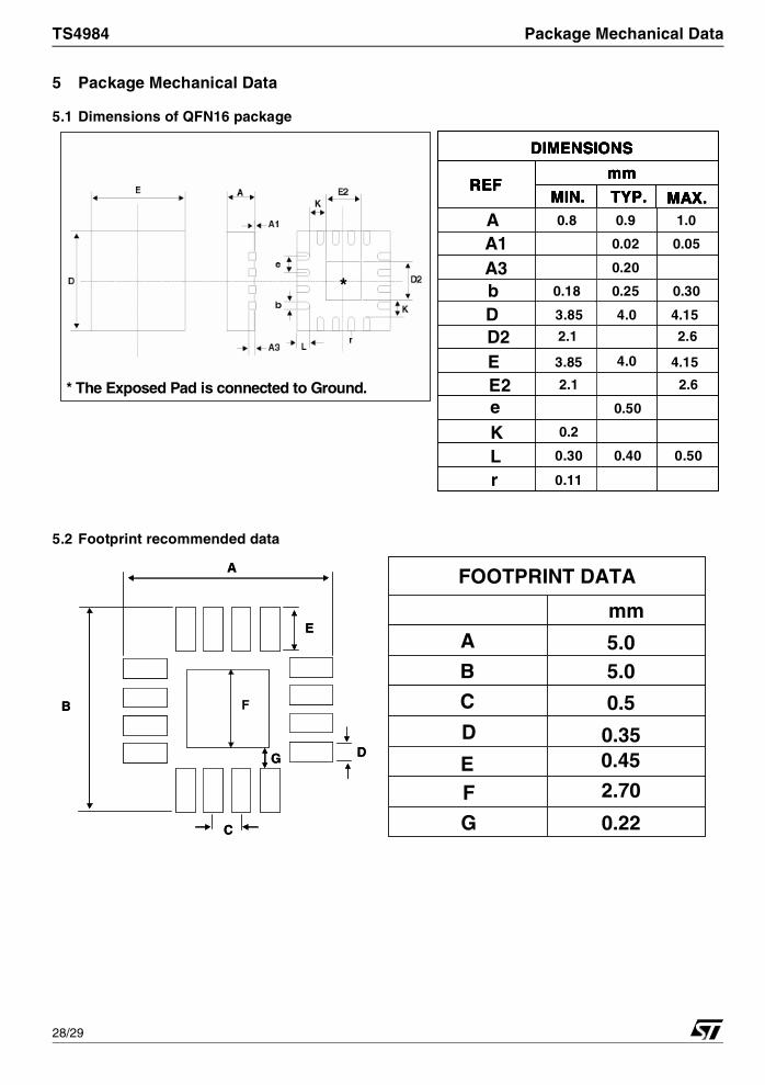
5 Package Mechanical Data
5.1 Dimensions of QFN16 package
5.2 Footprint recommended data
* The Exposed Pad is connected to Ground.
*
* The Exposed Pad is connected to Ground.
*
DIMENSIONS
REFmm
MIN. TYP. MAX.AA1A3bDD2EE2eKLr
0.9 1.00.8
0.02 0.05
0.20
0.25 0.300.18
4.0
2.62.1
4.0
2.62.1
0.50
0.2
0.40 0.500.30
0.11
3.85
3.85
4.15
4.15
DIMENSIONS
REFmm
MIN. TYP. MAX.AA1A3bDD2EE2eKLr
0.9 1.00.8
0.02 0.05
0.20
0.25 0.300.18
4.0
2.62.1
4.0
2.62.1
0.50
0.2
0.40 0.500.30
DIMENSIONS
REFmm
MIN. TYP. MAX.
DIMENSIONS
REFmm
MIN. TYP. MAX.AA1A3bDD2EE2eKLr
0.9 1.00.8
0.02 0.05
0.20
0.25 0.300.18
4.0
2.62.1
4.0
2.62.1
0.50
0.2
0.40 0.500.30
0.11
3.85
3.85
4.15
4.15
FOOTPRINT DATA
mm
A
B
C
D
EF
G 0.22
5.05.0
0.5
0.350.45
2.70
FOOTPRINT DATA
mm
A
B
C
D
EF
G 0.22
5.05.0
0.5
0.350.45
2.70
C
B
A
E
D
F
G
C
B
A
E
D
F
G
28/29
TS4984 Revision History
6 Revision History
Date Revision Description of Changes
01 Jan 2005 1 First Release
29/29
Information furnished is believed to be accurate and reliable. However, STMicroelectronics assumes no responsibility for the consequencesof use of such information nor for any infringement of patents or other rights of third parties which may result from its use. No license is grantedby implication or otherwise under any patent or patent rights of STMicroelectronics. Specifications mentioned in this publication are subjectto change without notice. This publication supersedes and replaces all information previously supplied. STMicroelectronics products are notauthorized for use as critical components in life support devices or systems without express written approval of STMicroelectronics.
The ST logo is a registered trademark of STMicroelectronicsAll other names are the property of their respective owners
© 2004 STMicroelectronics - All rights reserved
STMicroelectronics group of companiesAustralia - Belgium - Brazil - Canada - China - Czech Republic - Finland - France - Germany - Hong Kong - India - Israel - Italy - Japan -
Malaysia - Malta - Morocco - Singapore - Spain - Sweden - Switzerland - United Kingdom - United States of Americawww.st.com
Information furnished is believed to be accurate and reliable. However, STMicroelectronics assumes no responsibility for the consequencesof use of such information nor for any infringement of patents or other rights of third parties which may result from its use. No license is grantedby implication or otherwise under any patent or patent rights of STMicroelectronics. Specifications mentioned in this publication are subjectto change without notice. This publication supersedes and replaces all information previously supplied. STMicroelectronics products are notauthorized for use as critical components in life support devices or systems without express written approval of STMicroelectronics.
The ST logo is a registered trademark of STMicroelectronicsAll other names are the property of their respective owners
© 2005 STMicroelectronics - All rights reserved
STMicroelectronics group of companiesAustralia - Belgium - Brazil - Canada - China - Czech Republic - Finland - France - Germany - Hong Kong - India - Israel - Italy - Japan -
Malaysia - Malta - Morocco - Singapore - Spain - Sweden - Switzerland - United Kingdom - United States of Americawww.st.com