25AA320A/25LC320A 32K SPI Bus Serial EEPROM Data Sheet
30
© 2009 Microchip Technology Inc. DS21828F-page 1 25AA320A/25LC320A Device Selection Table Features: • Max. Clock 10 MHz • Low-Power CMOS Technology - Max. Write Current: 5 mA at 5.5V, 10 MHz - Read Current: 5 mA at 5.5V, 10 MHz - Standby Current: 5 μA at 5.5V • 4096 x 8-bit Organization • 32-Byte Page • Self-Timed Erase and Write Cycles (5 ms max.) • Block Write Protection - Protect none, 1/4, 1/2 or all of array • Built-in Write Protection - Power-on/off data protection circuitry - Write enable latch - Write-protect pin • Sequential Read • High Reliability - Endurance: >1M erase/write cycles - Data retention: > 200 years - ESD protection: > 4000V • Temperature Ranges Supported; • Pb-Free and RoHS Compliant Description: The Microchip Technology Inc. 25AA320A/25LC320A (25XX320A * ) are 32 kbit Serial Electrically Erasable PROMs. The memory is accessed via a simple Serial Peripheral Interface (SPI) compatible serial bus. The bus signals required are a clock input (SCK) plus sep- arate data in (SI) and data out (SO) lines. Access to the device is controlled through a Chip Select (CS ) input. Communication to the device can be paused via the hold pin (HOLD ). While the device is paused, transi- tions on its inputs will be ignored, with the exception of Chip Select, allowing the host to service higher priority interrupts. The 25XX320A is available in standard packages including 8-lead PDIP and SOIC, and advanced packaging including 8-lead MSOP, TSSOP and 2x3 TDFN. Package Types (not to scale) Part Number VCC Range Page Size Temp. Ranges Packages 25LC320A 2.5-5.5V 32 Byte I,E P, SN, ST, MS, MNY 25AA320A 1.8-5.5V 32 Byte I P, SN, ST, MS, MNY - Industrial (I): -40°C to +85°C - Automotive (E): -40°C to +125°C CS SO WP VSS 1 2 3 4 8 7 6 5 VCC HOLD SCK SI PDIP/SOIC (P, SN) TSSOP/MSOP CS SO WP VSS 1 2 3 4 8 7 6 5 VCC HOLD SCK SI (ST, MS) TDFN CS SO WP VSS HOLD SCK SI 5 6 7 8 4 3 2 1 VCC (MNY) X-Rotated TSSOP HOLD VCC CS SO 1 2 3 4 8 7 6 5 SCK SI VSS WP (X/ST) 32K SPI Bus Serial EEPROM *25XX320A is used in this document as a generic part number for the 25AA320A, 25LC320A devices.
Transcript of 25AA320A/25LC320A 32K SPI Bus Serial EEPROM Data Sheet

25AA320A/25LC320A32K SPI Bus Serial EEPROM
Device Selection Table
Features:• Max. Clock 10 MHz• Low-Power CMOS Technology
- Max. Write Current: 5 mA at 5.5V, 10 MHz- Read Current: 5 mA at 5.5V, 10 MHz- Standby Current: 5 μA at 5.5V
• 4096 x 8-bit Organization• 32-Byte Page• Self-Timed Erase and Write Cycles (5 ms max.)• Block Write Protection
- Protect none, 1/4, 1/2 or all of array• Built-in Write Protection
- Power-on/off data protection circuitry- Write enable latch- Write-protect pin
• Sequential Read• High Reliability
- Endurance: >1M erase/write cycles- Data retention: > 200 years- ESD protection: > 4000V
• Temperature Ranges Supported;
• Pb-Free and RoHS Compliant
Description:The Microchip Technology Inc. 25AA320A/25LC320A(25XX320A*) are 32 kbit Serial Electrically ErasablePROMs. The memory is accessed via a simple SerialPeripheral Interface (SPI) compatible serial bus. Thebus signals required are a clock input (SCK) plus sep-arate data in (SI) and data out (SO) lines. Access to thedevice is controlled through a Chip Select (CS) input.
Communication to the device can be paused via thehold pin (HOLD). While the device is paused, transi-tions on its inputs will be ignored, with the exception ofChip Select, allowing the host to service higher priorityinterrupts.
The 25XX320A is available in standard packagesincluding 8-lead PDIP and SOIC, and advancedpackaging including 8-lead MSOP, TSSOP and 2x3TDFN.
Package Types (not to scale)
Part Number VCC Range Page Size Temp. Ranges Packages
25LC320A 2.5-5.5V 32 Byte I,E P, SN, ST, MS, MNY25AA320A 1.8-5.5V 32 Byte I P, SN, ST, MS, MNY
- Industrial (I): -40°C to +85°C- Automotive (E): -40°C to +125°C
CSSOWPVSS
1234
8765
VCC
HOLDSCKSI
PDIP/SOIC(P, SN)
TSSOP/MSOP
CSSOWPVSS
1234
8765
VCCHOLDSCKSI
(ST, MS)
TDFN
CSSOWP
VSS
HOLDSCKSI5
6
7
8
4
3
2
1 VCC
(MNY)X-Rotated TSSOP
HOLDVCC
CSSO
1234
8765
SCKSIVSSWP
(X/ST)
*25XX320A is used in this document as a generic part numberfor the 25AA320A, 25LC320A devices.
© 2009 Microchip Technology Inc. DS21828F-page 1
25AA320A/25LC320A
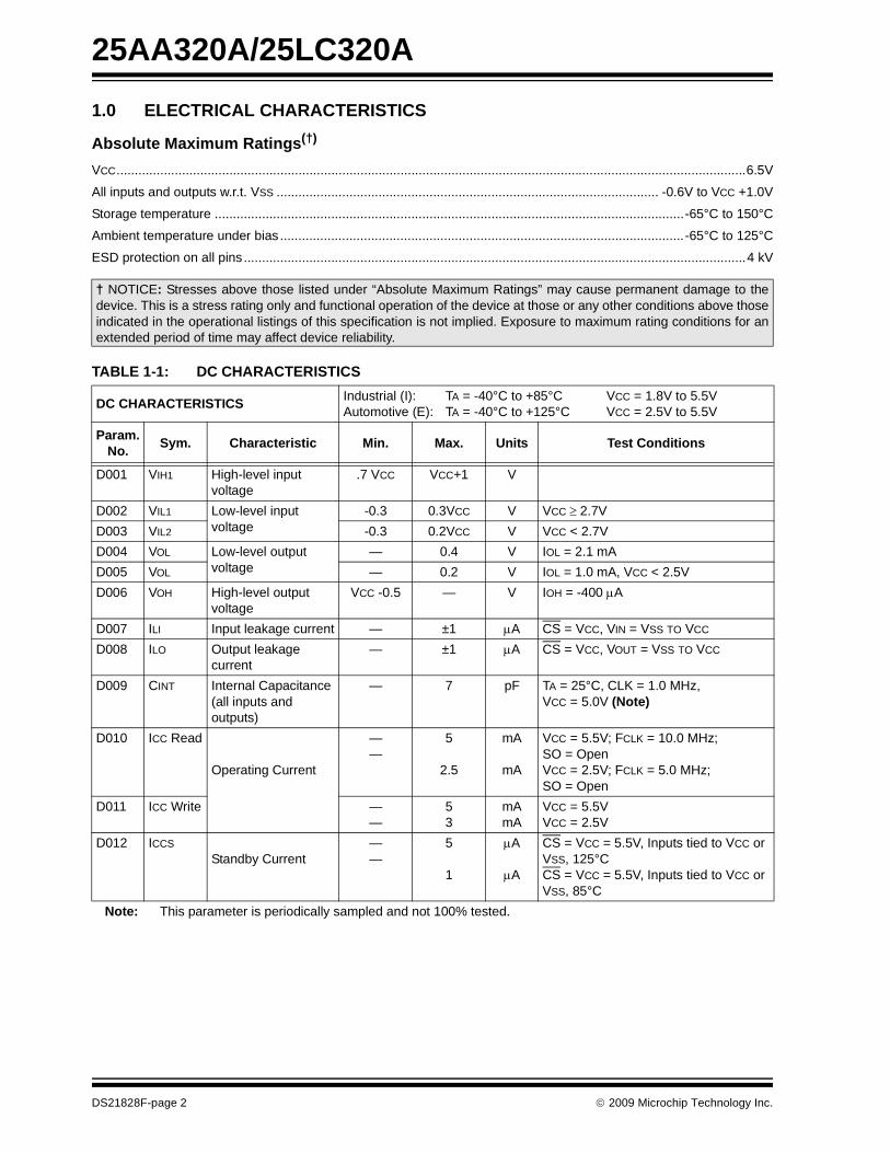
1.0 ELECTRICAL CHARACTERISTICS
Absolute Maximum Ratings(†)
VCC.............................................................................................................................................................................6.5V
All inputs and outputs w.r.t. VSS ......................................................................................................... -0.6V to VCC +1.0V
Storage temperature .................................................................................................................................-65°C to 150°C
Ambient temperature under bias ...............................................................................................................-65°C to 125°C
ESD protection on all pins ..........................................................................................................................................4 kV
TABLE 1-1: DC CHARACTERISTICS
† NOTICE: Stresses above those listed under “Absolute Maximum Ratings” may cause permanent damage to thedevice. This is a stress rating only and functional operation of the device at those or any other conditions above thoseindicated in the operational listings of this specification is not implied. Exposure to maximum rating conditions for anextended period of time may affect device reliability.
DC CHARACTERISTICS Industrial (I): TA = -40°C to +85°C VCC = 1.8V to 5.5VAutomotive (E): TA = -40°C to +125°C VCC = 2.5V to 5.5V
Param.No. Sym. Characteristic Min. Max. Units Test Conditions
D001 VIH1 High-level input voltage
.7 VCC VCC+1 V
D002 VIL1 Low-level inputvoltage
-0.3 0.3VCC V VCC ≥ 2.7VD003 VIL2 -0.3 0.2VCC V VCC < 2.7VD004 VOL Low-level output
voltage— 0.4 V IOL = 2.1 mA
D005 VOL — 0.2 V IOL = 1.0 mA, VCC < 2.5VD006 VOH High-level output
voltageVCC -0.5 — V IOH = -400 μA
D007 ILI Input leakage current — ±1 μA CS = VCC, VIN = VSS TO VCC
D008 ILO Output leakage current
— ±1 μA CS = VCC, VOUT = VSS TO VCC
D009 CINT Internal Capacitance(all inputs and outputs)
— 7 pF TA = 25°C, CLK = 1.0 MHz,VCC = 5.0V (Note)
D010 ICC Read
Operating Current
——
5
2.5
mA
mA
VCC = 5.5V; FCLK = 10.0 MHz; SO = OpenVCC = 2.5V; FCLK = 5.0 MHz; SO = Open
D011 ICC Write ——
53
mAmA
VCC = 5.5VVCC = 2.5V
D012 ICCSStandby Current
——
5
1
μA
μA
CS = VCC = 5.5V, Inputs tied to VCC or VSS, 125°CCS = VCC = 5.5V, Inputs tied to VCC or VSS, 85°C
Note: This parameter is periodically sampled and not 100% tested.
DS21828F-page 2 © 2009 Microchip Technology Inc.
25AA320A/25LC320A
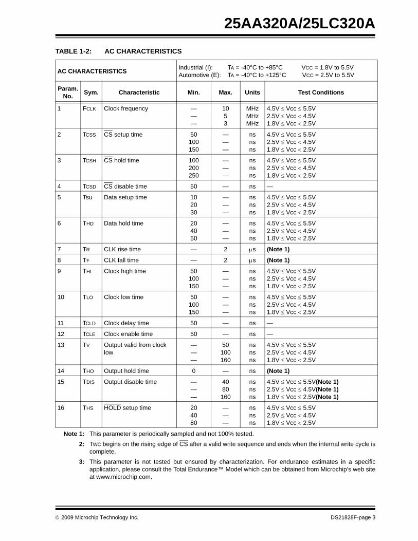
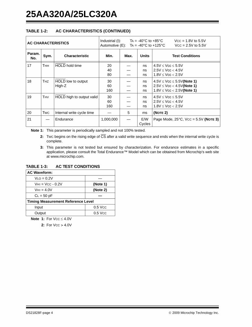
TABLE 1-2: AC CHARACTERISTICSAC CHARACTERISTICS Industrial (I): TA = -40°C to +85°C VCC = 1.8V to 5.5VAutomotive (E): TA = -40°C to +125°C VCC = 2.5V to 5.5V
Param.No. Sym. Characteristic Min. Max. Units Test Conditions
1 FCLK Clock frequency ———
1053
MHzMHzMHz
4.5V ≤ Vcc ≤ 5.5V2.5V ≤ Vcc < 4.5V1.8V ≤ Vcc < 2.5V
2 TCSS CS setup time 50100150
———
nsnsns
4.5V ≤ Vcc ≤ 5.5V2.5V ≤ Vcc < 4.5V1.8V ≤ Vcc < 2.5V
3 TCSH CS hold time 100200250
———
nsnsns
4.5V ≤ Vcc ≤ 5.5V2.5V ≤ Vcc < 4.5V1.8V ≤ Vcc < 2.5V
4 TCSD CS disable time 50 — ns —
5 Tsu Data setup time 102030
———
nsnsns
4.5V ≤ Vcc ≤ 5.5V2.5V ≤ Vcc < 4.5V1.8V ≤ Vcc < 2.5V
6 THD Data hold time 204050
———
nsnsns
4.5V ≤ Vcc ≤ 5.5V2.5V ≤ Vcc < 4.5V1.8V ≤ Vcc < 2.5V
7 TR CLK rise time — 2 μs (Note 1)
8 TF CLK fall time — 2 μs (Note 1)
9 THI Clock high time 50100150
———
nsnsns
4.5V ≤ Vcc ≤ 5.5V2.5V ≤ Vcc < 4.5V1.8V ≤ Vcc < 2.5V
10 TLO Clock low time 50100150
———
nsnsns
4.5V ≤ Vcc ≤ 5.5V2.5V ≤ Vcc < 4.5V1.8V ≤ Vcc < 2.5V
11 TCLD Clock delay time 50 — ns —
12 TCLE Clock enable time 50 — ns —
13 TV Output valid from clock low
———
50100160
nsnsns
4.5V ≤ Vcc ≤ 5.5V2.5V ≤ Vcc < 4.5V1.8V ≤ Vcc < 2.5V
14 THO Output hold time 0 — ns (Note 1)
15 TDIS Output disable time ———
4080
160
nsnsns
4.5V ≤ Vcc ≤ 5.5V(Note 1)2.5V ≤ Vcc ≤ 4.5V(Note 1)1.8V ≤ Vcc ≤ 2.5V(Note 1)
16 THS HOLD setup time 204080
———
nsnsns
4.5V ≤ Vcc ≤ 5.5V2.5V ≤ Vcc < 4.5V1.8V ≤ Vcc < 2.5V
Note 1: This parameter is periodically sampled and not 100% tested.
2: TWC begins on the rising edge of CS after a valid write sequence and ends when the internal write cycle iscomplete.
3: This parameter is not tested but ensured by characterization. For endurance estimates in a specificapplication, please consult the Total Endurance™ Model which can be obtained from Microchip’s web siteat www.microchip.com.
© 2009 Microchip Technology Inc. DS21828F-page 3
25AA320A/25LC320A
TABLE 1-3: AC TEST CONDITIONS
17 THH HOLD hold time 204080
———
nsnsns
4.5V ≤ Vcc ≤ 5.5V2.5V ≤ Vcc < 4.5V1.8V ≤ Vcc < 2.5V
18 THZ HOLD low to output High-Z
3060
160
———
nsnsns
4.5V ≤ Vcc ≤ 5.5V(Note 1)2.5V ≤ Vcc < 4.5V(Note 1)1.8V ≤ Vcc < 2.5V(Note 1)
19 THV HOLD high to output valid 3060
160
———
nsnsns
4.5V ≤ Vcc ≤ 5.5V2.5V ≤ Vcc < 4.5V1.8V ≤ Vcc < 2.5V
20 TWC Internal write cycle time — 5 ms (NOTE 2)
21 — Endurance 1,000,000 — E/W Cycles
Page Mode, 25°C, VCC = 5.5V (NOTE 3)
TABLE 1-2: AC CHARACTERISTICS (CONTINUED)
AC CHARACTERISTICS Industrial (I): TA = -40°C to +85°C VCC = 1.8V to 5.5VAutomotive (E): TA = -40°C to +125°C VCC = 2.5V to 5.5V
Param.No. Sym. Characteristic Min. Max. Units Test Conditions
Note 1: This parameter is periodically sampled and not 100% tested.
2: TWC begins on the rising edge of CS after a valid write sequence and ends when the internal write cycle iscomplete.
3: This parameter is not tested but ensured by characterization. For endurance estimates in a specificapplication, please consult the Total Endurance™ Model which can be obtained from Microchip’s web siteat www.microchip.com.
AC Waveform: VLO = 0.2V —VHI = VCC - 0.2V (Note 1)VHI = 4.0V (Note 2)CL = 50 pF —
Timing Measurement Reference LevelInput 0.5 VCC
Output 0.5 VCC
Note 1: For VCC ≤ 4.0V
2: For VCC > 4.0V
DS21828F-page 4 © 2009 Microchip Technology Inc.
25AA320A/25LC320A
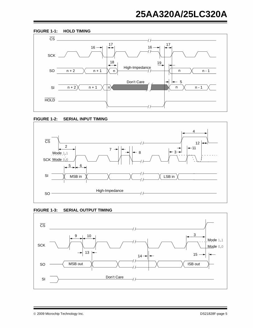
FIGURE 1-1: HOLD TIMINGFIGURE 1-2: SERIAL INPUT TIMING
FIGURE 1-3: SERIAL OUTPUT TIMING
CS
SCK
SO
SI
HOLD
1716 16
17
1918
Don’t Care 5
High-Impedancen + 2 n + 1 n n - 1n
n + 2 n + 1 n n n - 1
CS
SCK
SI
SO
65
87 11
3
LSB inMSB in
High-Impedance
12
Mode 1,1
Mode 0,0
2
4
CS
SCK
SO
109
13
MSB out ISB out
3
15
Don’t CareSI
Mode 1,1
Mode 0,0
14
© 2009 Microchip Technology Inc. DS21828F-page 5
25AA320A/25LC320A
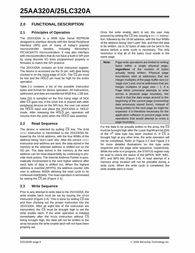
2.0 FUNCTIONAL DESCRIPTION
2.1 Principles of OperationThe 25XX320A is a 4096 byte Serial EEPROMdesigned to interface directly with the Serial PeripheralInterface (SPI) port of many of today’s popularmicrocontroller families, including Microchip’sPIC16C6X/7X microcontrollers. It may also interfacewith microcontrollers that do not have a built-in SPI portby using discrete I/O lines programmed properly infirmware to match the SPI protocol.
The 25XX320A contains an 8-bit instruction register.The device is accessed via the SI pin, with data beingclocked in on the rising edge of SCK. The CS pin mustbe low and the HOLD pin must be high for the entireoperation.
Table 2-1 contains a list of the possible instructionbytes and format for device operation. All instructions,addresses and data are transferred MSB first, LSB last.
Data (SI) is sampled on the first rising edge of SCKafter CS goes low. If the clock line is shared with otherperipheral devices on the SPI bus, the user can assertthe HOLD input and place the 25XX320A in ‘HOLD’mode. After releasing the HOLD pin, operation willresume from the point when the HOLD was asserted.
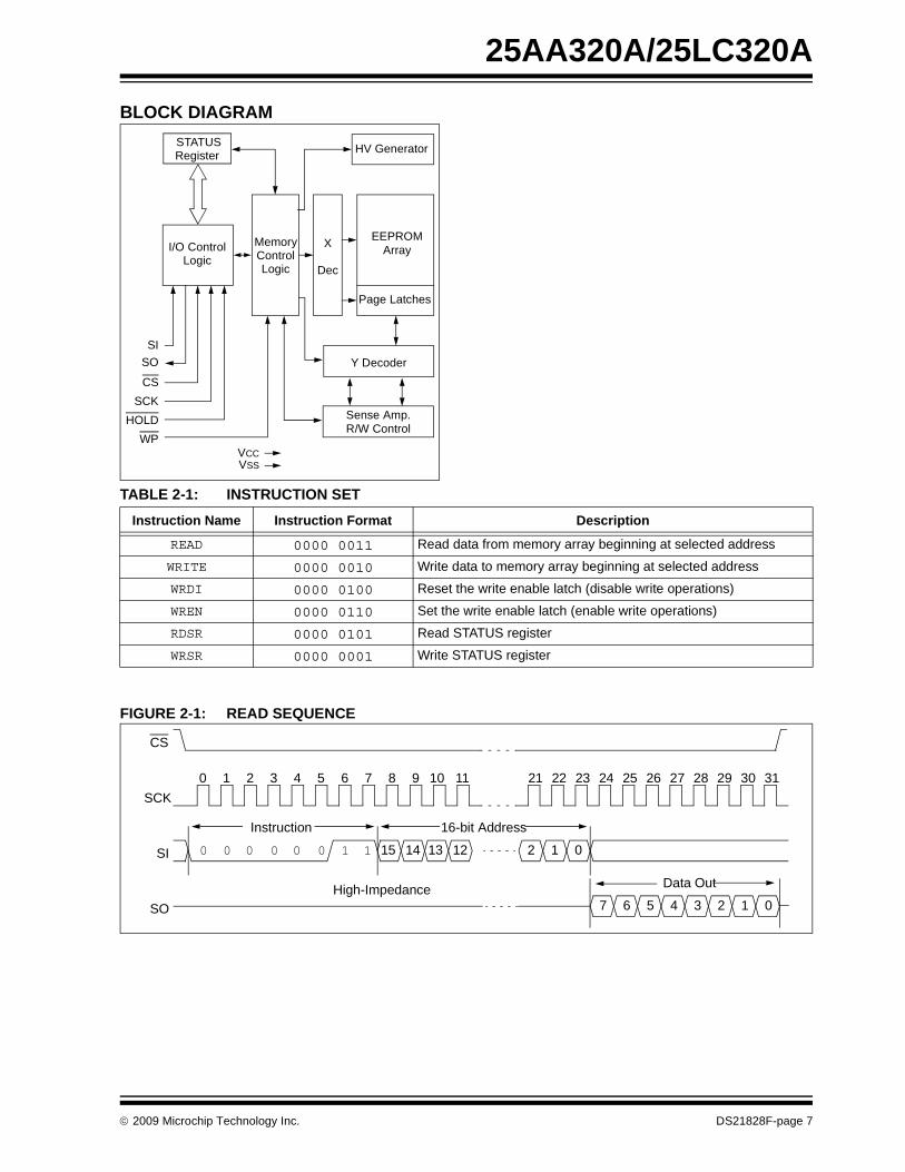
2.2 Read SequenceThe device is selected by pulling CS low. The 8-bitREAD instruction is transmitted to the 25XX320A fol-lowed by the 16-bit address, with the four MSBs of theaddress being “don’t care” bits. After the correct READinstruction and address are sent, the data stored in thememory at the selected address is shifted out on theSO pin. The data stored in the memory at the nextaddress can be read sequentially by continuing to pro-vide clock pulses. The internal Address Pointer is auto-matically incremented to the next higher address aftereach byte of data is shifted out. When the highestaddress is reached (0FFFh), the address counter rollsover to address 0000h allowing the read cycle to becontinued indefinitely. The read operation is terminatedby raising the CS pin (Figure 2-1).
2.3 Write SequencePrior to any attempt to write data to the 25XX320A, thewrite enable latch must be set by issuing the WRENinstruction (Figure 2-4). This is done by setting CS lowand then clocking out the proper instruction into the25XX320A. After all eight bits of the instruction aretransmitted, the CS must be brought high to set thewrite enable latch. If the write operation is initiatedimmediately after the WREN instruction without CSbeing brought high, the data will not be written to thearray because the write enable latch will not have beenproperly set.
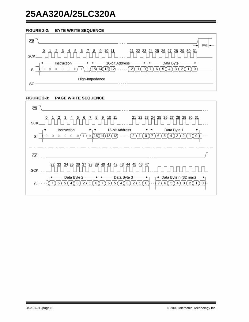
Once the write enable latch is set, the user mayproceed by setting the CS low, issuing a WRITE instruc-tion, followed by the 16-bit address, with the four MSBsof the address being “don’t care” bits, and then the datato be written. Up to 32 bytes of data can be sent to thedevice before a write cycle is necessary. The onlyrestriction is that all of the bytes must reside in thesame page.
For the data to be actually written to the array, the CSmust be brought high after the Least Significant bit (D0)of the nth data byte has been clocked in. If CS isbrought high at any other time, the write operation willnot be completed. Refer to Figure 2-2 and Figure 2-3for more detailed illustrations on the byte writesequence and the page write sequence, respectively.While the write is in progress, the STATUS register maybe read to check the status of the WPEN, WIP, WEL,BP1 and BP0 bits (Figure 2-6). A read attempt of amemory array location will not be possible during awrite cycle. When the write cycle is completed, thewrite enable latch is reset.
Note: Page write operations are limited to writingbytes within a single physical page,regardless of the number of bytesactually being written. Physical pageboundaries start at addresses that areinteger multiples of the page buffer size (or‘page size’) and, end at addresses that areinteger multiples of page size – 1. If aPage Write command attempts to writeacross a physical page boundary, theresult is that the data wraps around to thebeginning of the current page (overwritingdata previously stored there), instead ofbeing written to the next page as might beexpected. It is therefore necessary for theapplication software to prevent page writeoperations that would attempt to cross apage boundary.
DS21828F-page 6 © 2009 Microchip Technology Inc.
25AA320A/25LC320A
BLOCK DIAGRAM
FIGURE 2-1: READ SEQUENCE
SISO
SCKCS
HOLDWP
STATUSRegister
I/O Control MemoryControlLogic
X
Dec
HV Generator
EEPROMArray
Page Latches
Y Decoder
Sense Amp.R/W Control
Logic
VCCVSS
TABLE 2-1: INSTRUCTION SET
Instruction Name Instruction Format Description
READ 0000 0011 Read data from memory array beginning at selected address
WRITE 0000 0010 Write data to memory array beginning at selected address
WRDI 0000 0100 Reset the write enable latch (disable write operations)
WREN 0000 0110 Set the write enable latch (enable write operations)
RDSR 0000 0101 Read STATUS register
WRSR 0000 0001 Write STATUS register
SO
SI
SCK
CS
0 2 3 4 5 6 7 8 9 10 11 21 22 23 24 25 26 27 28 29 30 311
0 100000 1 15 14 13 12 2 1 0
7 6 5 4 3 2 1 0
Instruction 16-bit Address
Data OutHigh-Impedance
© 2009 Microchip Technology Inc. DS21828F-page 7
25AA320A/25LC320A
FIGURE 2-2: BYTE WRITE SEQUENCEFIGURE 2-3: PAGE WRITE SEQUENCE
SO
SI
CS
9 10 11 21 22 23 24 25 26 27 28 29 30 31
0 000000 1 15 14 13 12 2 1 0 7 6 5 4 3 2 1 0Instruction 16-bit Address Data Byte
High-Impedance
SCK0 2 3 4 5 6 71 8
Twc
SI
CS
9 10 11 21 22 23 24 25 26 27 28 29 30 31
0 000000 1 15 14 13 12 2 1 0 7 6 5 4 3 2 1 0Instruction 16-bit Address Data Byte 1
SCK0 2 3 4 5 6 71 8
SI
CS
41 42 43 46 47
7 6 5 4 3 2 1 0Data Byte n (32 max)
SCK32 34 35 36 37 38 3933 40
7 6 5 4 3 2 1 0Data Byte 3
7 6 5 4 3 2 1 0Data Byte 2
44 45
DS21828F-page 8 © 2009 Microchip Technology Inc.
25AA320A/25LC320A
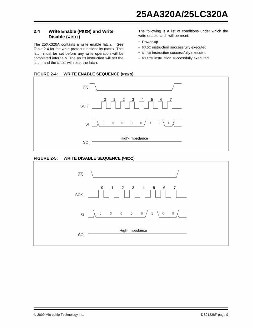
2.4 Write Enable (WREN) and WriteDisable (WRDI)The 25XX320A contains a write enable latch. SeeTable 2-4 for the write-protect functionality matrix. Thislatch must be set before any write operation will becompleted internally. The WREN instruction will set thelatch, and the WRDI will reset the latch.
The following is a list of conditions under which thewrite enable latch will be reset:
• Power-up• WRDI instruction successfully executed• WRSR instruction successfully executed• WRITE instruction successfully executed
FIGURE 2-4: WRITE ENABLE SEQUENCE (WREN)
FIGURE 2-5: WRITE DISABLE SEQUENCE (WRDI)
SCK
0 2 3 4 5 6 71
SI
High-ImpedanceSO
CS
0 10 0 0 0 01
SCK
0 2 3 4 5 6 71
SI
High-ImpedanceSO
CS
0 10 0 0 0 010
© 2009 Microchip Technology Inc. DS21828F-page 9
25AA320A/25LC320A
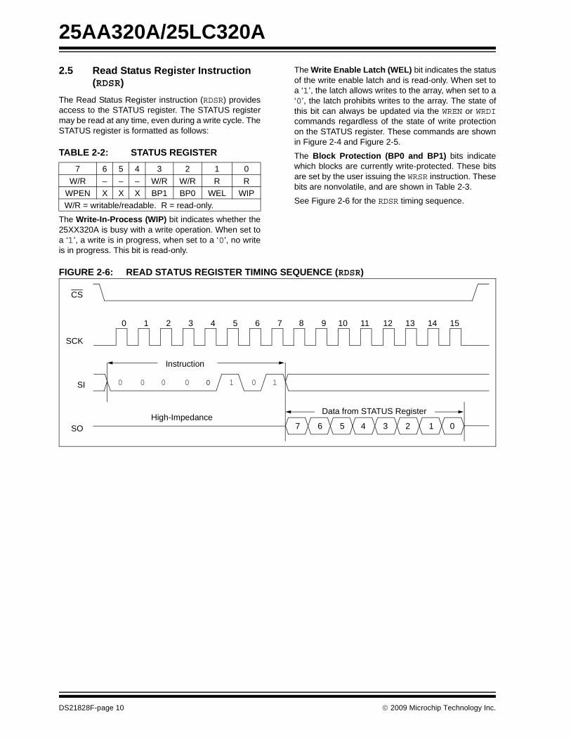
2.5 Read Status Register Instruction(RDSR)The Read Status Register instruction (RDSR) providesaccess to the STATUS register. The STATUS registermay be read at any time, even during a write cycle. TheSTATUS register is formatted as follows:
TABLE 2-2: STATUS REGISTER
The Write-In-Process (WIP) bit indicates whether the25XX320A is busy with a write operation. When set toa ‘1’, a write is in progress, when set to a ‘0’, no writeis in progress. This bit is read-only.
The Write Enable Latch (WEL) bit indicates the statusof the write enable latch and is read-only. When set toa ‘1’, the latch allows writes to the array, when set to a‘0’, the latch prohibits writes to the array. The state ofthis bit can always be updated via the WREN or WRDIcommands regardless of the state of write protectionon the STATUS register. These commands are shownin Figure 2-4 and Figure 2-5.
The Block Protection (BP0 and BP1) bits indicatewhich blocks are currently write-protected. These bitsare set by the user issuing the WRSR instruction. Thesebits are nonvolatile, and are shown in Table 2-3.
See Figure 2-6 for the RDSR timing sequence.
FIGURE 2-6: READ STATUS REGISTER TIMING SEQUENCE (RDSR)
7 6 5 4 3 2 1 0W/R – – – W/R W/R R R
WPEN X X X BP1 BP0 WEL WIPW/R = writable/readable. R = read-only.
SO
SI
CS
9 10 11 12 13 14 15
1 100000 0
7 6 5 4 2 1 0
Instruction
Data from STATUS RegisterHigh-Impedance
SCK
0 2 3 4 5 6 71 8
3
DS21828F-page 10 © 2009 Microchip Technology Inc.
25AA320A/25LC320A
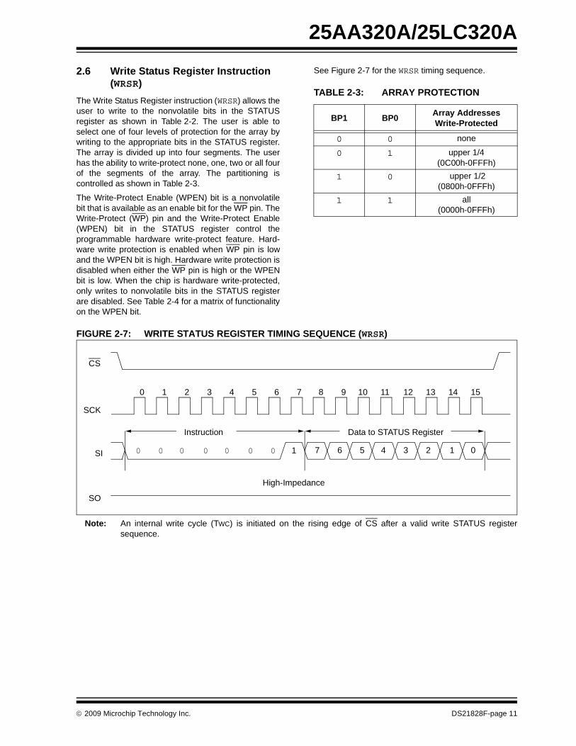
2.6 Write Status Register Instruction(WRSR)The Write Status Register instruction (WRSR) allows theuser to write to the nonvolatile bits in the STATUSregister as shown in Table 2-2. The user is able toselect one of four levels of protection for the array bywriting to the appropriate bits in the STATUS register.The array is divided up into four segments. The userhas the ability to write-protect none, one, two or all fourof the segments of the array. The partitioning iscontrolled as shown in Table 2-3.
The Write-Protect Enable (WPEN) bit is a nonvolatilebit that is available as an enable bit for the WP pin. TheWrite-Protect (WP) pin and the Write-Protect Enable(WPEN) bit in the STATUS register control theprogrammable hardware write-protect feature. Hard-ware write protection is enabled when WP pin is lowand the WPEN bit is high. Hardware write protection isdisabled when either the WP pin is high or the WPENbit is low. When the chip is hardware write-protected,only writes to nonvolatile bits in the STATUS registerare disabled. See Table 2-4 for a matrix of functionalityon the WPEN bit.
See Figure 2-7 for the WRSR timing sequence.
TABLE 2-3: ARRAY PROTECTION
FIGURE 2-7: WRITE STATUS REGISTER TIMING SEQUENCE (WRSR)
BP1 BP0 Array AddressesWrite-Protected
0 0 none
0 1 upper 1/4(0C00h-0FFFh)
1 0 upper 1/2(0800h-0FFFh)
1 1 all(0000h-0FFFh)
SO
SI
CS
9 10 11 12 13 14 15
0 100000 0 7 6 5 4 2 1 0
Instruction Data to STATUS Register
High-Impedance
SCK
0 2 3 4 5 6 71 8
3
Note: An internal write cycle (TWC) is initiated on the rising edge of CS after a valid write STATUS registersequence.
© 2009 Microchip Technology Inc. DS21828F-page 11
25AA320A/25LC320A
2.7 Data ProtectionThe following protection has been implemented toprevent inadvertent writes to the array:• The write enable latch is reset on power-up• A write enable instruction must be issued to set
the write enable latch• After a byte write, page write or STATUS register
write, the write enable latch is reset• CS must be set high after the proper number of
clock cycles to start an internal write cycle• Access to the array during an internal write cycle
is ignored and programming is continued
2.8 Power-On StateThe 25XX320A powers on in the following state:
• The device is in low-power Standby mode (CS =1)
• The write enable latch is reset• SO is in high-impedance state• A high-to-low-level transition on CS is required to
enter active state
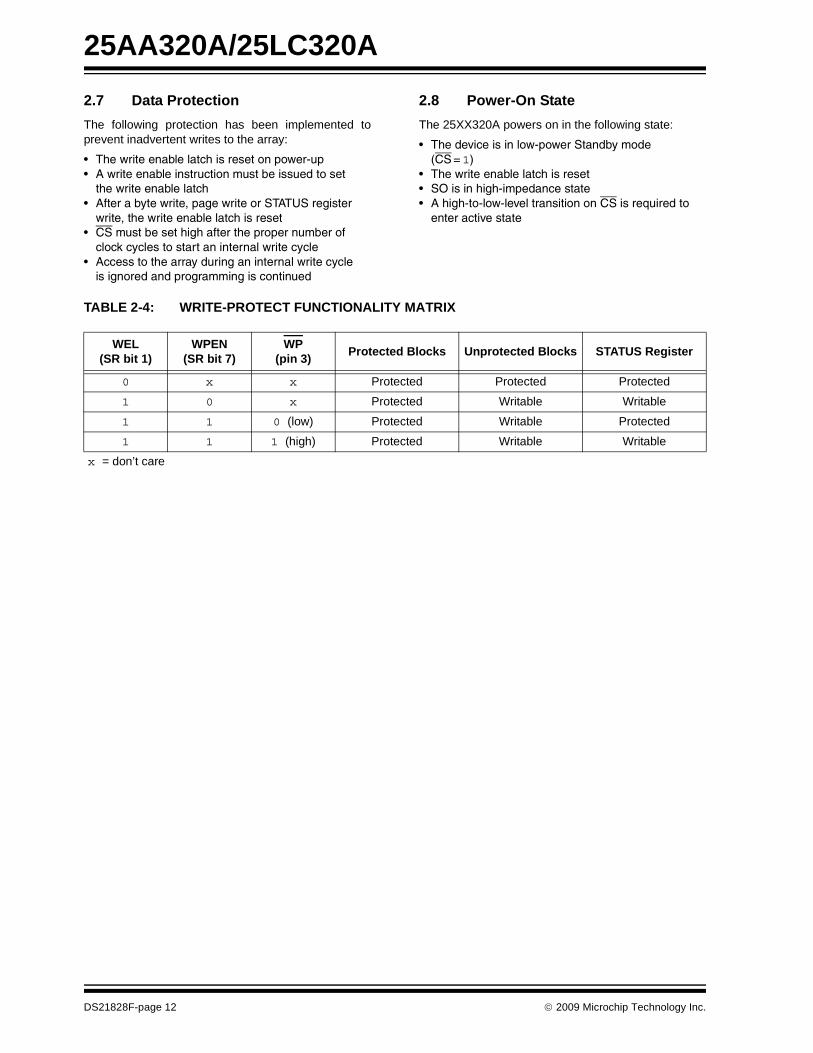
TABLE 2-4: WRITE-PROTECT FUNCTIONALITY MATRIX
WEL(SR bit 1)
WPEN(SR bit 7)
WP(pin 3) Protected Blocks Unprotected Blocks STATUS Register
0 x x Protected Protected Protected
1 0 x Protected Writable Writable
1 1 0 (low) Protected Writable Protected
1 1 1 (high) Protected Writable Writable
x = don’t care
DS21828F-page 12 © 2009 Microchip Technology Inc.
25AA320A/25LC320A
3.0 PIN DESCRIPTIONSThe descriptions of the pins are listed in Table 3-1.
TABLE 3-1: PIN FUNCTION TABLE
3.1 Chip Select (CS)A low level on this pin selects the device. A high leveldeselects the device and forces it into Standby mode.However, a programming cycle which is alreadyinitiated or in progress will be completed, regardless ofthe CS input signal. If CS is brought high during aprogram cycle, the device will go into Standby mode assoon as the programming cycle is complete. When thedevice is deselected, SO goes to the high-impedancestate, allowing multiple parts to share the same SPIbus. A low-to-high transition on CS after a valid writesequence initiates an internal write cycle. After power-up, a low level on CS is required prior to any sequencebeing initiated.
3.2 Serial Output (SO)The SO pin is used to transfer data out of the25XX320A. During a read cycle, data is shifted out onthis pin after the falling edge of the serial clock.
3.3 Write-Protect (WP)This pin is used in conjunction with the WPEN bit in theSTATUS register to prohibit writes to the nonvolatilebits in the STATUS register. When WP is low andWPEN is high, writing to the nonvolatile bits in the STA-TUS register is disabled. All other operations functionnormally. When WP is high, all functions, includingwrites to the nonvolatile bits in the STATUS registeroperate normally. If the WPEN bit is set, WP low duringa STATUS register write sequence will disable writingto the STATUS register. If an internal write cycle hasalready begun, WP going low will have no effect on thewrite.
The WP pin function is blocked when the WPEN bit inthe STATUS register is low. This allows the user toinstall the 25XX320A in a system with WP pingrounded and still be able to write to the STATUSregister. The WP pin functions will be enabled when theWPEN bit is set high.
3.4 Serial Input (SI)The SI pin is used to transfer data into the device. Itreceives instructions, addresses and data. Data islatched on the rising edge of the serial clock.
3.5 Serial Clock (SCK)The SCK is used to synchronize the communicationbetween a master and the 25XX320A. Instructions,addresses or data present on the SI pin are latched onthe rising edge of the clock input, while data on the SOpin is updated after the falling edge of the clock input.
3.6 Hold (HOLD)The HOLD pin is used to suspend transmission to the25XX320A while in the middle of a serial sequencewithout having to retransmit the entire sequence again.It must be held high any time this function is not beingused. Once the device is selected and a serialsequence is underway, the HOLD pin may be pulledlow to pause further serial communication withoutresetting the serial sequence. The HOLD pin must bebrought low while SCK is low, otherwise the HOLDfunction will not be invoked until the next SCK high-to-low transition. The 25XX320A must remain selectedduring this sequence. The SI, SCK and SO pins are ina high-impedance state during the time the device ispaused and transitions on these pins will be ignored. Toresume serial communication, HOLD must be broughthigh while the SCK pin is low, otherwise serialcommunication will not resume. Lowering the HOLDline at any time will tri-state the SO line.
Name Pin Number
X-Rotated Pin
Number
Function
CS 1 3 Chip Select InputSO 2 4 Serial Data OutputWP 3 5 Write-Protect PinVSS 4 6 GroundSI 5 7 Serial Data Input
SCK 6 8 Serial Clock InputHOLD 7 1 Hold InputVCC 8 2 Supply VoltageNote: The exposed pad on the TDFN package
can be connected to VSS or left floating.
© 2009 Microchip Technology Inc. DS21828F-page 13
25AA320A/25LC320A
4.0 PACKAGING INFORMATION
4.1 Package Marking Information
8-Lead MSOP (150 mil) Example:
XXXXXTYWWNNN
5LBAI 3281L7
T/XXXNNNXXXXXXXX
YYWW
8-Lead PDIP
8-Lead SOIC
XXXXYYWWXXXXXXXT
NNN
XXXXTYWW
8-Lead TSSOP
NNN
I/P 1L725LC320A
0328
Example:
Example:
SN 072825LC32AI
1L7
1L7
5LBAI328
Example:
3e
3e
8-Lead 2x3 TDFN Example:
XXXYWWNN
C7182817
TSSOP 1st Line Marking
Device std mark
25AA320A 5ABA25AA320AX ABAX25LC320A 5LBA25LC320AX LBAX
MSOP 1st Line Marking
Device std mark
25AA320A 5ABAT25LC320A 5LBAT
TDFN 1st Line Marking
Device std mark
25AA320A-I C7125LC320A-E C7425LC320A-I C75
DS21828F-page 14 © 2009 Microchip Technology Inc.
25AA320A/25LC320A
Note: Custom marking available.
Legend: XX...X Customer-specific informationY Year code (last digit of calendar year)YY Year code (last 2 digits of calendar year)WW Week code (week of January 1 is week ‘01’)NNN Alphanumeric traceability code Pb-free JEDEC designator for Matte Tin (Sn)* This package is Pb-free. The Pb-free JEDEC designator ( )
can be found on the outer packaging for this package.
Note: In the event the full Microchip part number cannot be marked on one line, it willbe carried over to the next line, thus limiting the number of availablecharacters for customer-specific information.
3e
3e
© 2009 Microchip Technology Inc. DS21828F-page 15
25AA320A/25LC320A
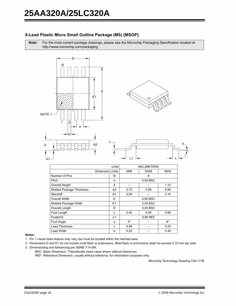
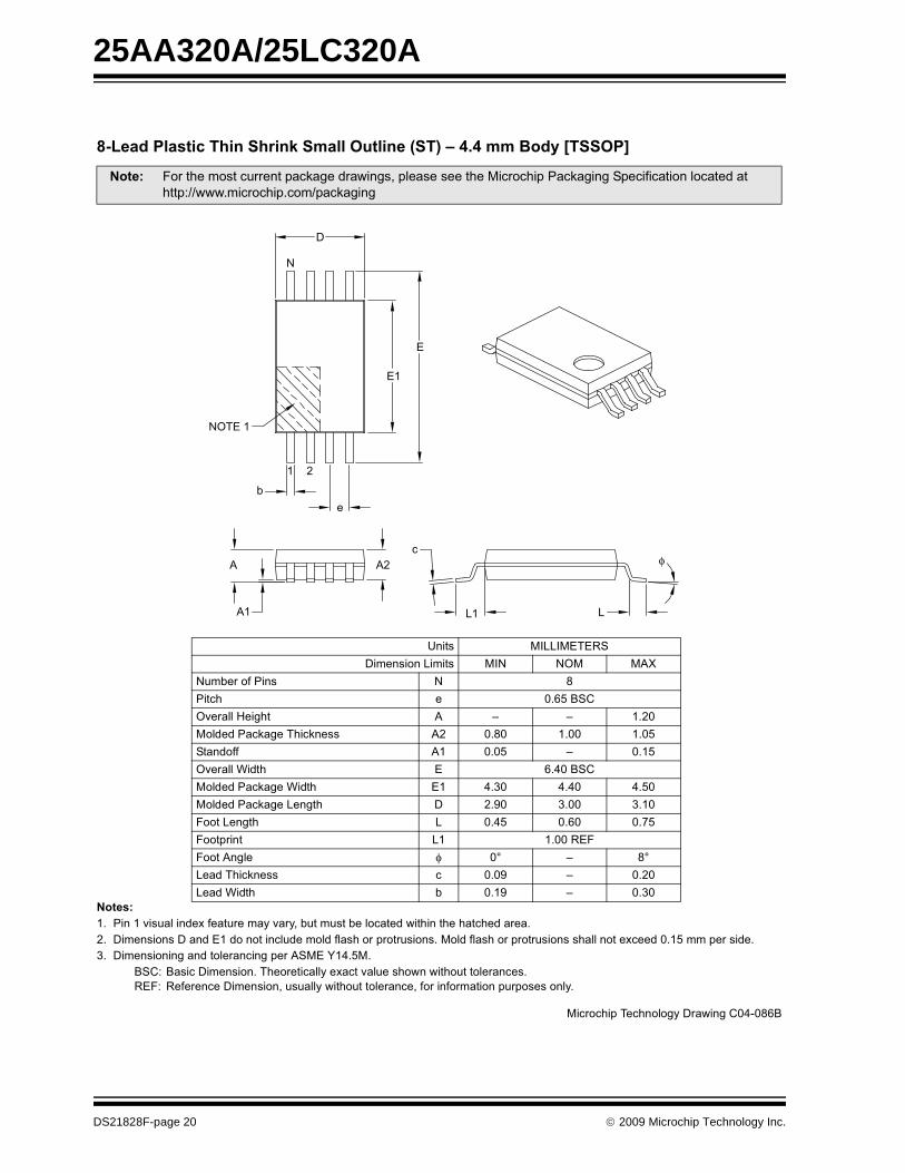
���������� ��� ����������� ��������������������
�������� �������� !�����"�#�$��%!��&������'�(!%�&! %�(�����%�"�)�%����%�����%���"������� ��&�� �� �����"�*��"��%�����!"��&�"�$�� ����%! �� ����"�$�� ����%! �� � ������%��#���"����+�&&���� �"��,� ��&�� ��������"�%���������������*�-���+��
.�/0 .� �����&�� ���� ���%��������#��%����!�� �)��)�%�!%�%������ ��*10 ��$��������&�� ��'�! !�����)�%�!%�%������'�$���$&�%����!� � �����
����� 1�%���& %��!��%����2����"�)��� '����� �� ���%��������������2�����������$���%������%�"��%��%%�033)))�&��������&3���2�����
4��% ��55��* *����&�� ���5�&�% ��6 67� ��8
6!&(��$���� 6 9��%�� � ��:+�.�/7������;����% � < < ������"�"����2���� ���2�� �� ���+ ��9+ ���+�%��"$$� �� ���� < ���+7������=�"%� * �����.�/��"�"����2����=�"%� *� ,����.�/7������5���%� � ,����.�/1%�5���%� 5 ���� ��:� ��9�1%���% 5� ���+��*11%������ � �> < 9>5��"� ���2�� � ���9 < ���,5��"�=�"%� ( ���� < ����
D
N
E
E1
NOTE 1
1 2e
b
A
A1
A2c
L1 L
φ
������� ������� ��)��� /������.
DS21828F-page 16 © 2009 Microchip Technology Inc.
25AA320A/25LC320A
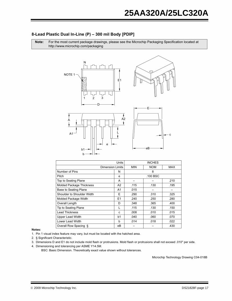
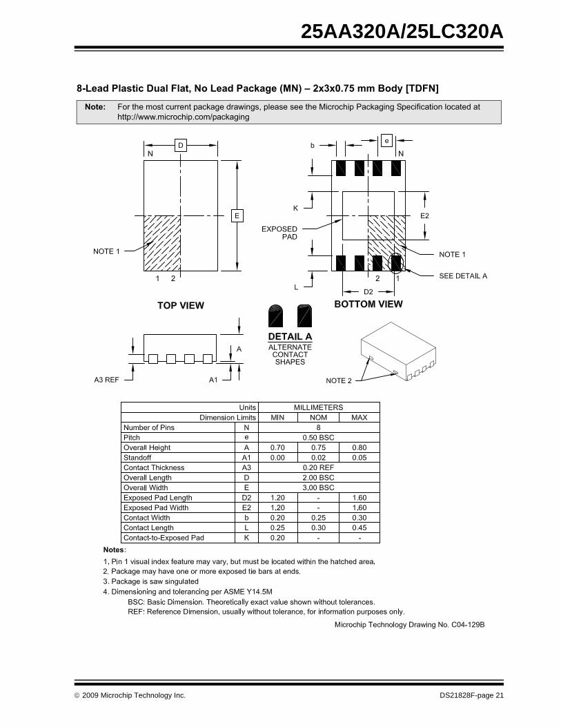
���������� ������ ��� ������!�"##�� �$��%��� �
�������� �������� !�����"�#�$��%!��&������'�(!%�&! %�(�����%�"�)�%��%�����%���"������� ?������$����%�/����%�� %���,� ��&�� �� �����"�*��"��%�����!"��&�"�$�� ����%! �� ����"�$�� ����%! �� � ������%��#���"�����@���� �"���� ��&�� ��������"�%���������������*�-���+��
.�/0�.� �����&�� ���� ���%��������#��%����!�� �)��)�%�!%�%������ �
����� 1�%���& %��!��%����2����"�)��� '����� �� ���%��������������2�����������$���%������%�"��%��%%�033)))�&��������&3���2�����
4��% �6/;*���&�� ���5�&�% ��6 67� ��8
6!&(��$���� 6 9��%�� � �����.�/ ��%����%��������� � < < ������"�"����2���� ���2�� �� ���+ ��,� ���+.� ��%����%��������� �� ���+ < <��!�"��%���!�"��=�"%� * ���� �,�� �,�+��"�"����2����=�"%� *� ���� ��+� ��9�7������5���%� � �,�9 �,:+ ���� ���%����%��������� 5 ���+ ��,� ��+�5��"� ���2�� � ���9 ���� ���+4����5��"�=�"%� (� ���� ��:� ����5)��5��"�=�"%� ( ���� ���9 ����7�������)����������? �. < < ��,�
N
E1
NOTE 1
D
1 2 3
A
A1
A2
L
b1b
e
E
eB
c
������� ������� ��)��� /�����9.
© 2009 Microchip Technology Inc. DS21828F-page 17
25AA320A/25LC320A
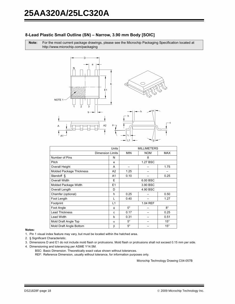
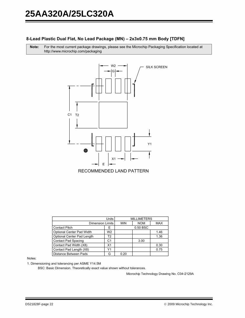
���������� ��������� ��������!������&'�"()#����$��%���� *�
�������� �������� !�����"�#�$��%!��&������'�(!%�&! %�(�����%�"�)�%����%�����%���"������� ?������$����%�/����%�� %���,� ��&�� �� �����"�*��"��%�����!"��&�"�$�� ����%! �� ����"�$�� ����%! �� � ������%��#���"����+�&&���� �"���� ��&�� ��������"�%���������������*�-���+��
.�/0 .� �����&�� ���� ���%��������#��%����!�� �)��)�%�!%�%������ ��*10 ��$��������&�� ��'�! !�����)�%�!%�%������'�$���$&�%����!� � �����
����� 1�%���& %��!��%����2����"�)��� '����� �� ���%��������������2�����������$���%������%�"��%��%%�033)))�&��������&3���2�����
4��% ��55��* *����&�� ���5�&�% ��6 67� ��8
6!&(��$���� 6 9��%�� � �����.�/7������;����% � < < ���+��"�"����2���� ���2�� �� ���+ < <�%��"$$��? �� ���� < ���+7������=�"%� * :����.�/��"�"����2����=�"%� *� ,����.�/7������5���%� � �����.�//��&$��A�%����B � ���+ < ��+�1%�5���%� 5 ���� < ����1%���% 5� ������*11%������ � �> < 9>5��"� ���2�� � ���� < ���+5��"�=�"%� ( ��,� < ��+���"���$%������� � � +> < �+>��"���$%�������.%%& � +> < �+>
D
Ne
E
E1
NOTE 1
1 2 3
b
A
A1
A2
L
L1
c
h
h
φ
β
α
������� ������� ��)��� /����+�.
DS21828F-page 18 © 2009 Microchip Technology Inc.
25AA320A/25LC320A
���������� ��������� ��������!������&'�"()#����$��%���� *�
����� 1�%���& %��!��%����2����"�)��� '����� �� ���%��������������2�����������$���%������%�"��%��%%�033)))�&��������&3���2�����
© 2009 Microchip Technology Inc. DS21828F-page 19
25AA320A/25LC320A
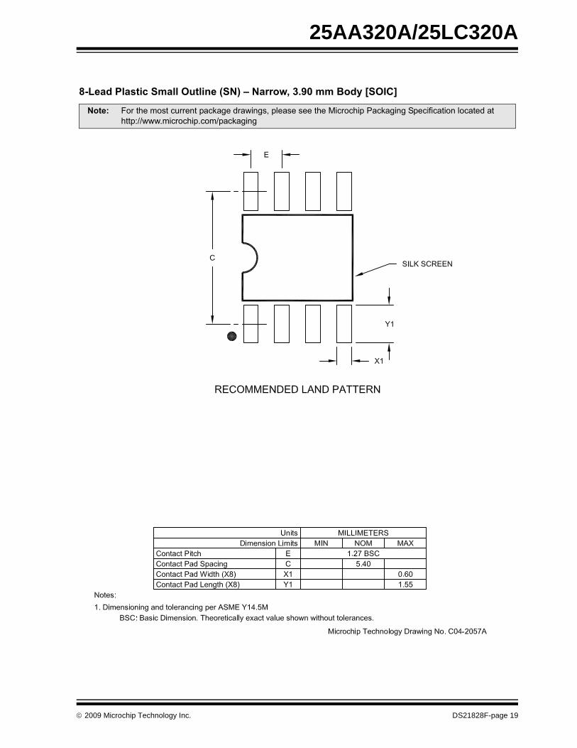
���������� ��+, ���,� ���������� �����+��!�-(-����$��%��+����
�������� �������� !�����"�#�$��%!��&������'�(!%�&! %�(�����%�"�)�%����%�����%���"������� ��&�� �� �����"�*��"��%�����!"��&�"�$�� ����%! �� ����"�$�� ����%! �� � ������%��#���"����+�&&���� �"��,� ��&�� ��������"�%���������������*�-���+��
.�/0 .� �����&�� ���� ���%��������#��%����!�� �)��)�%�!%�%������ ��*10 ��$��������&�� ��'�! !�����)�%�!%�%������'�$���$&�%����!� � �����
����� 1�%���& %��!��%����2����"�)��� '����� �� ���%��������������2�����������$���%������%�"��%��%%�033)))�&��������&3���2�����
4��% ��55��* *����&�� ���5�&�% ��6 67� ��8
6!&(��$���� 6 9��%�� � ��:+�.�/7������;����% � < < ������"�"����2���� ���2�� �� ��9� ���� ���+�%��"$$� �� ���+ < ���+7������=�"%� * :����.�/��"�"����2����=�"%� *� ��,� ���� ��+���"�"����2����5���%� � ���� ,��� ,���1%�5���%� 5 ���+ ��:� ���+1%���% 5� ������*11%������ � �> < 9>5��"� ���2�� � ���� < ����5��"�=�"%� ( ���� < ��,�
D
N
E
E1
NOTE 1
1 2
be
cA
A1
A2
L1 L
φ
������� ������� ��)��� /����9:.
DS21828F-page 20 © 2009 Microchip Technology Inc.
25AA320A/25LC320A
���������� ������.��'���������������������!�/0"0#(12����$��%��+�.��
����� 1�%���& %��!��%����2����"�)��� '����� �� ���%��������������2�����������$���%������%�"��%��%%�033)))�&��������&3���2�����
© 2009 Microchip Technology Inc. DS21828F-page 21
25AA320A/25LC320A
���������� ������.��'���������������������!�/0"0#(12����$��%��+�.��
����� 1�%���& %��!��%����2����"�)��� '����� �� ���%��������������2�����������$���%������%�"��%��%%�033)))�&��������&3���2�����
DS21828F-page 22 © 2009 Microchip Technology Inc.
25AA320A/25LC320A
APPENDIX A: REVISION HISTORY
Revision BCorrections to Section 1.0, Electrical Characteristics.
Revision C (02/07)Deleted X-Rotated TSSOP; Revised Table 1-3;Revised Packaging Information; Replaced PackageDrawings; Revised Product ID System.
Revision D (03/07)Replaced Package Drawings (Rev. AM).
Revision E (10/08)Added TDFN Package; Revised Table 3-1, PinFunction Table; Updated Package Drawings.
Revision F (06/09)Added X-Rotated TSSOP to package types; RevisedTable 1-2, Param. 21; Revised Table 3-1; RevisedTSSOP Line Marking table; Revised Product IDsection.
© 2009 Microchip Technology Inc. DS21828F-page 23

25AA320A/25LC320A
NOTES:DS21828F-page 24 © 2009 Microchip Technology Inc.
25AA320A/25LC320A
THE MICROCHIP WEB SITEMicrochip provides online support via our WWW site atwww.microchip.com. This web site is used as a meansto make files and information easily available tocustomers. Accessible by using your favorite Internetbrowser, the web site contains the followinginformation:
• Product Support – Data sheets and errata, application notes and sample programs, design resources, user’s guides and hardware support documents, latest software releases and archived software
• General Technical Support – Frequently Asked Questions (FAQ), technical support requests, online discussion groups, Microchip consultant program member listing
• Business of Microchip – Product selector and ordering guides, latest Microchip press releases, listing of seminars and events, listings of Microchip sales offices, distributors and factory representatives
CUSTOMER CHANGE NOTIFICATION SERVICEMicrochip’s customer notification service helps keepcustomers current on Microchip products. Subscriberswill receive e-mail notification whenever there arechanges, updates, revisions or errata related to aspecified product family or development tool of interest.
To register, access the Microchip web site atwww.microchip.com, click on Customer ChangeNotification and follow the registration instructions.
CUSTOMER SUPPORTUsers of Microchip products can receive assistancethrough several channels:
• Distributor or Representative• Local Sales Office• Field Application Engineer (FAE)• Technical Support• Development Systems Information Line
Customers should contact their distributor,representative or field application engineer (FAE) forsupport. Local sales offices are also available to helpcustomers. A listing of sales offices and locations isincluded in the back of this document.
Technical support is available through the web siteat: http://support.microchip.com
© 2009 Microchip Technology Inc. DS21828F-page 25

25AA320A/25LC320A
READER RESPONSEIt is our intention to provide you with the best documentation possible to ensure successful use of your Microchip prod-uct. If you wish to provide your comments on organization, clarity, subject matter, and ways in which our documentationcan better serve you, please FAX your comments to the Technical Publications Manager at (480) 792-4150.
Please list the following information, and use this outline to provide us with your comments about this document.
To: Technical Publications Manager
RE: Reader ResponseTotal Pages Sent ________
From: Name
CompanyAddressCity / State / ZIP / Country
Telephone: (_______) _________ - _________
Application (optional):
Would you like a reply? Y N
Device: Literature Number:
Questions:
FAX: (______) _________ - _________
DS21828F25AA320A/25LC320A
1. What are the best features of this document?
2. How does this document meet your hardware and software development needs?
3. Do you find the organization of this document easy to follow? If not, why?
4. What additions to the document do you think would enhance the structure and subject?
5. What deletions from the document could be made without affecting the overall usefulness?
6. Is there any incorrect or misleading information (what and where)?
7. How would you improve this document?
DS21828F-page 26 © 2009 Microchip Technology Inc.
25AA320A/25LC320A
PRODUCT IDENTIFICATION SYSTEMTo order or obtain information, e.g., on pricing or delivery, refer to the factory or the listed sales office.
PART NO. X /XX
PackageTape & ReelDevice
Device: 25AA320A =
25LC320A = 25AA320AX =
25LC320AX =
32k-bit, 1.8V, SPI Serial EEPROM32k-bit, 2.5V, SPI Serial EEPROM32k-bit, 1.8V, SPI Serial EEPROM in alternate pinout (ST only)32k-bit, 2.5V, SPI Serial EEPROM in alternate pinout (ST only)
Tape & Reel: Blank = T =
Standard packagingTape & Reel
Temperature Range:
I =E =
-40°C to+85°C-40°C to+125°C
Package: MS =P =SN =ST =MNY(1) =
Plastic MSOP (Micro Small Outline), 8-leadPlastic DIP (300 mil body), 8-leadPlastic SOIC (3.90 mm body), 8-leadTSSOP, 8-leadTDFN, 8-lead 2x3 mm
Note 1: “Y” indicates a Nickel Palladium Gold (NiPdAu) finish.
Examples:a) 25AA320A-I/MS = 32k-bit, 1.8V Serial
EEPROM, Industrial temp., MSOP package
b) 25AA320AT-I/SN = 32k-bit, 1.8V SerialEEPROM, Industrial temp., Tape & Reel, SOICpackage
c) 25LC320AT-E/SN = 32k-bit, 2.5V SerialEEPROM, Extended temp., Tape & Reel, SOICpackage
d) 25LC320AT-I/ST = 32k-bit, 2.5V SerialEEPROM, Industrial temp., Tape & Reel,TSSOP package
e) 25LC320AXT-I/ST = 32k-bit, 2.5V SerialEEPROM, Industrial temp., Tape & Reel,Rotated pinout, TSSOP package
– X
Temp Range
© 2009 Microchip Technology Inc. DS21828F-page 27
25AA320A/25LC320A
NOTES:DS21828F-page 28 © 2009 Microchip Technology Inc.
Note the following details of the code protection feature on Microchip devices:• Microchip products meet the specification contained in their particular Microchip Data Sheet.
• Microchip believes that its family of products is one of the most secure families of its kind on the market today, when used in the intended manner and under normal conditions.
• There are dishonest and possibly illegal methods used to breach the code protection feature. All of these methods, to our knowledge, require using the Microchip products in a manner outside the operating specifications contained in Microchip’s Data Sheets. Most likely, the person doing so is engaged in theft of intellectual property.
• Microchip is willing to work with the customer who is concerned about the integrity of their code.
• Neither Microchip nor any other semiconductor manufacturer can guarantee the security of their code. Code protection does not mean that we are guaranteeing the product as “unbreakable.”
Code protection is constantly evolving. We at Microchip are committed to continuously improving the code protection features of ourproducts. Attempts to break Microchip’s code protection feature may be a violation of the Digital Millennium Copyright Act. If such actsallow unauthorized access to your software or other copyrighted work, you may have a right to sue for relief under that Act.
Information contained in this publication regarding deviceapplications and the like is provided only for your convenienceand may be superseded by updates. It is your responsibility toensure that your application meets with your specifications.MICROCHIP MAKES NO REPRESENTATIONS ORWARRANTIES OF ANY KIND WHETHER EXPRESS ORIMPLIED, WRITTEN OR ORAL, STATUTORY OROTHERWISE, RELATED TO THE INFORMATION,INCLUDING BUT NOT LIMITED TO ITS CONDITION,QUALITY, PERFORMANCE, MERCHANTABILITY ORFITNESS FOR PURPOSE. Microchip disclaims all liabilityarising from this information and its use. Use of Microchipdevices in life support and/or safety applications is entirely atthe buyer’s risk, and the buyer agrees to defend, indemnify andhold harmless Microchip from any and all damages, claims,suits, or expenses resulting from such use. No licenses areconveyed, implicitly or otherwise, under any Microchipintellectual property rights.
© 2009 Microchip Technology Inc.
Trademarks
The Microchip name and logo, the Microchip logo, dsPIC, KEELOQ, KEELOQ logo, MPLAB, PIC, PICmicro, PICSTART, rfPIC and UNI/O are registered trademarks of Microchip Technology Incorporated in the U.S.A. and other countries.
FilterLab, Hampshire, HI-TECH C, Linear Active Thermistor, MXDEV, MXLAB, SEEVAL and The Embedded Control Solutions Company are registered trademarks of Microchip Technology Incorporated in the U.S.A.
Analog-for-the-Digital Age, Application Maestro, CodeGuard, dsPICDEM, dsPICDEM.net, dsPICworks, dsSPEAK, ECAN, ECONOMONITOR, FanSense, HI-TIDE, In-Circuit Serial Programming, ICSP, ICEPIC, Mindi, MiWi, MPASM, MPLAB Certified logo, MPLIB, MPLINK, mTouch, nanoWatt XLP, Omniscient Code Generation, PICC, PICC-18, PICkit, PICDEM, PICDEM.net, PICtail, PIC32 logo, REAL ICE, rfLAB, Select Mode, Total Endurance, TSHARC, WiperLock and ZENA are trademarks of Microchip Technology Incorporated in the U.S.A. and other countries.
SQTP is a service mark of Microchip Technology Incorporated in the U.S.A.
All other trademarks mentioned herein are property of their respective companies.
© 2009, Microchip Technology Incorporated, Printed in the U.S.A., All Rights Reserved.
Printed on recycled paper.
DS21828F-page 29
Microchip received ISO/TS-16949:2002 certification for its worldwide headquarters, design and wafer fabrication facilities in Chandler and Tempe, Arizona; Gresham, Oregon and design centers in California and India. The Company’s quality system processes and procedures are for its PIC® MCUs and dsPIC® DSCs, KEELOQ® code hopping devices, Serial EEPROMs, microperipherals, nonvolatile memory and analog products. In addition, Microchip’s quality system for the design and manufacture of development systems is ISO 9001:2000 certified.
DS21828F-page 30 © 2009 Microchip Technology Inc.
AMERICASCorporate Office2355 West Chandler Blvd.Chandler, AZ 85224-6199Tel: 480-792-7200 Fax: 480-792-7277Technical Support: http://support.microchip.comWeb Address: www.microchip.comAtlantaDuluth, GA Tel: 678-957-9614 Fax: 678-957-1455BostonWestborough, MA Tel: 774-760-0087 Fax: 774-760-0088ChicagoItasca, IL Tel: 630-285-0071 Fax: 630-285-0075ClevelandIndependence, OH Tel: 216-447-0464 Fax: 216-447-0643DallasAddison, TX Tel: 972-818-7423 Fax: 972-818-2924DetroitFarmington Hills, MI Tel: 248-538-2250Fax: 248-538-2260KokomoKokomo, IN Tel: 765-864-8360Fax: 765-864-8387Los AngelesMission Viejo, CA Tel: 949-462-9523 Fax: 949-462-9608Santa ClaraSanta Clara, CA Tel: 408-961-6444Fax: 408-961-6445TorontoMississauga, Ontario, CanadaTel: 905-673-0699 Fax: 905-673-6509
ASIA/PACIFICAsia Pacific OfficeSuites 3707-14, 37th FloorTower 6, The GatewayHarbour City, KowloonHong KongTel: 852-2401-1200Fax: 852-2401-3431Australia - SydneyTel: 61-2-9868-6733Fax: 61-2-9868-6755China - BeijingTel: 86-10-8528-2100 Fax: 86-10-8528-2104China - ChengduTel: 86-28-8665-5511Fax: 86-28-8665-7889China - Hong Kong SARTel: 852-2401-1200 Fax: 852-2401-3431China - NanjingTel: 86-25-8473-2460Fax: 86-25-8473-2470China - QingdaoTel: 86-532-8502-7355Fax: 86-532-8502-7205China - ShanghaiTel: 86-21-5407-5533 Fax: 86-21-5407-5066China - ShenyangTel: 86-24-2334-2829Fax: 86-24-2334-2393China - ShenzhenTel: 86-755-8203-2660 Fax: 86-755-8203-1760China - WuhanTel: 86-27-5980-5300Fax: 86-27-5980-5118China - XiamenTel: 86-592-2388138 Fax: 86-592-2388130China - XianTel: 86-29-8833-7252Fax: 86-29-8833-7256China - ZhuhaiTel: 86-756-3210040 Fax: 86-756-3210049
ASIA/PACIFICIndia - BangaloreTel: 91-80-3090-4444 Fax: 91-80-3090-4080India - New DelhiTel: 91-11-4160-8631Fax: 91-11-4160-8632India - PuneTel: 91-20-2566-1512Fax: 91-20-2566-1513Japan - YokohamaTel: 81-45-471- 6166 Fax: 81-45-471-6122Korea - DaeguTel: 82-53-744-4301Fax: 82-53-744-4302Korea - SeoulTel: 82-2-554-7200Fax: 82-2-558-5932 or 82-2-558-5934Malaysia - Kuala LumpurTel: 60-3-6201-9857Fax: 60-3-6201-9859Malaysia - PenangTel: 60-4-227-8870Fax: 60-4-227-4068Philippines - ManilaTel: 63-2-634-9065Fax: 63-2-634-9069SingaporeTel: 65-6334-8870Fax: 65-6334-8850Taiwan - Hsin ChuTel: 886-3-6578-300Fax: 886-3-6578-370Taiwan - KaohsiungTel: 886-7-536-4818Fax: 886-7-536-4803Taiwan - TaipeiTel: 886-2-2500-6610 Fax: 886-2-2508-0102Thailand - BangkokTel: 66-2-694-1351Fax: 66-2-694-1350
EUROPEAustria - WelsTel: 43-7242-2244-39Fax: 43-7242-2244-393Denmark - CopenhagenTel: 45-4450-2828 Fax: 45-4485-2829France - ParisTel: 33-1-69-53-63-20 Fax: 33-1-69-30-90-79Germany - MunichTel: 49-89-627-144-0 Fax: 49-89-627-144-44Italy - Milan Tel: 39-0331-742611 Fax: 39-0331-466781Netherlands - DrunenTel: 31-416-690399 Fax: 31-416-690340Spain - MadridTel: 34-91-708-08-90Fax: 34-91-708-08-91UK - WokinghamTel: 44-118-921-5869Fax: 44-118-921-5820
WORLDWIDE SALES AND SERVICE
03/26/09