2.1 Electrical characteristics (curves Sheets/ST Microelectronics PDFS/2N7000, 2N7002.pdfElectrical...
14
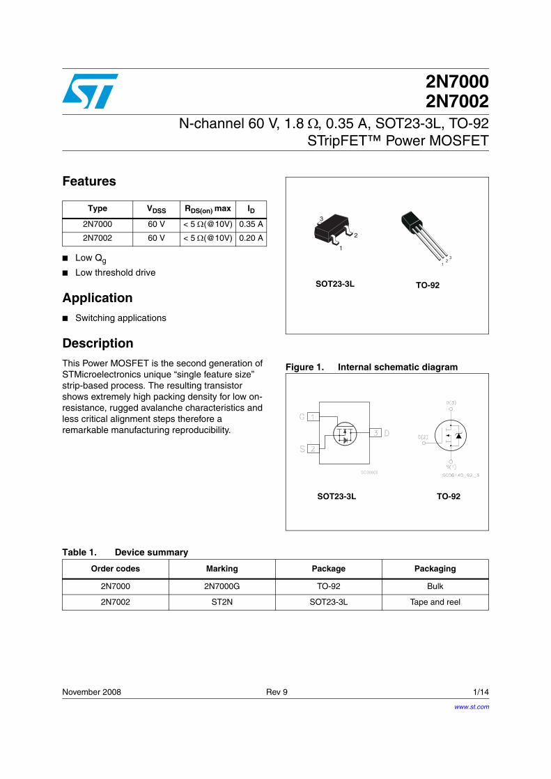
November 2008 Rev 9 1/14 14 2N7000 2N7002 N-channel 60 V, 1.8 Ω , 0.35 A, SOT23-3L, TO-92 STripFET™ Power MOSFET Features ■ Low Q g ■ Low threshold drive Application ■ Switching applications Description This Power MOSFET is the second generation of STMicroelectronics unique “single feature size” strip-based process. The resulting transistor shows extremely high packing density for low on- resistance, rugged avalanche characteristics and less critical alignment steps therefore a remarkable manufacturing reproducibility. Figure 1. Internal schematic diagram Type V DSS R DS(on) max I D 2N7000 60 V < 5 Ω(@10V) 0.35 A 2N7002 60 V < 5 Ω(@10V) 0.20 A 1 2 3 SOT23-3L TO-92 SOT23-3L TO-92 Table 1. Device summary Order codes Marking Package Packaging 2N7000 2N7000G TO-92 Bulk 2N7002 ST2N SOT23-3L Tape and reel www.st.com
Transcript of 2.1 Electrical characteristics (curves Sheets/ST Microelectronics PDFS/2N7000, 2N7002.pdfElectrical...
November 2008 Rev 9 1/14
14
2N70002N7002
N-channel 60 V, 1.8 Ω, 0.35 A, SOT23-3L, TO-92STripFET™ Power MOSFET
Features
Low Qg
Low threshold drive
Application Switching applications
DescriptionThis Power MOSFET is the second generation of STMicroelectronics unique “single feature size” strip-based process. The resulting transistor shows extremely high packing density for low on-resistance, rugged avalanche characteristics and less critical alignment steps therefore a remarkable manufacturing reproducibility.
Figure 1. Internal schematic diagram
Type VDSS RDS(on) max ID2N7000 60 V < 5 Ω(@10V) 0.35 A
2N7002 60 V < 5 Ω(@10V) 0.20 A1
2
3
SOT23-3L TO-92
SOT23-3L TO-92
Table 1. Device summary
Order codes Marking Package Packaging
2N7000 2N7000G TO-92 Bulk
2N7002 ST2N SOT23-3L Tape and reel
www.st.com
Contents 2N7000, 2N7002
2/14
Contents
1 Electrical ratings . . . . . . . . . . . . . . . . . . . . . . . . . . . . . . . . . . . . . . . . . . . . 3
2 Electrical characteristics . . . . . . . . . . . . . . . . . . . . . . . . . . . . . . . . . . . . . 42.1 Electrical characteristics (curves) . . . . . . . . . . . . . . . . . . . . . . . . . . . . 6
3 Test circuits . . . . . . . . . . . . . . . . . . . . . . . . . . . . . . . . . . . . . . . . . . . . . . 9
4 Package mechanical data . . . . . . . . . . . . . . . . . . . . . . . . . . . . . . . . . . . . 10
5 Revision history . . . . . . . . . . . . . . . . . . . . . . . . . . . . . . . . . . . . . . . . . . . 13
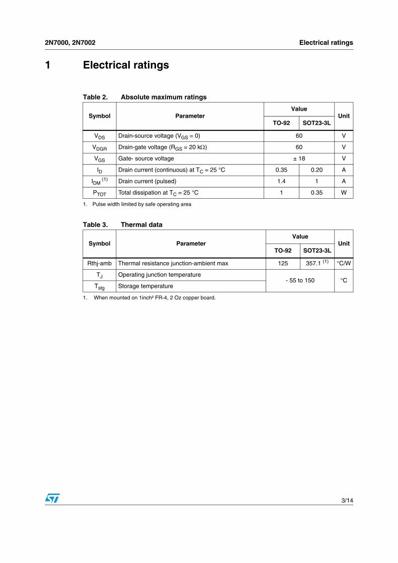
2N7000, 2N7002 Electrical ratings
3/14
1 Electrical ratings
Table 2. Absolute maximum ratings
Symbol ParameterValue
UnitTO-92 SOT23-3L
VDS Drain-source voltage (VGS = 0) 60 V
VDGR Drain-gate voltage (RGS = 20 kΩ) 60 V
VGS Gate- source voltage ± 18 V
ID Drain current (continuous) at TC = 25 °C 0.35 0.20 A
IDM (1)
1. Pulse width limited by safe operating area
Drain current (pulsed) 1.4 1 A
PTOT Total dissipation at TC = 25 °C 1 0.35 W
Table 3. Thermal data
Symbol ParameterValue
UnitTO-92 SOT23-3L
Rthj-amb Thermal resistance junction-ambient max 125 357.1 (1)
1. When mounted on 1inch² FR-4, 2 Oz copper board.
°C/W
TJ Operating junction temperature- 55 to 150 °C
Tstg Storage temperature
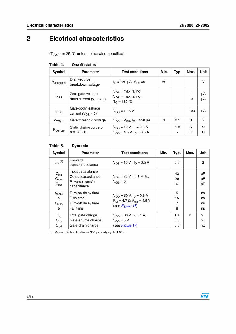
Electrical characteristics 2N7000, 2N7002
4/14
2 Electrical characteristics
(TCASE = 25 °C unless otherwise specified)
Table 4. On/off states
Symbol Parameter Test conditions Min. Typ. Max. Unit
V(BR)DSSDrain-source breakdown voltage
ID = 250 µA, VGS =0 60 V
IDSSZero gate voltage
drain current (VGS = 0)
VDS = max ratingVDS = max rating,
TC = 125 °C
1
10
µA
µA
IGSSGate-body leakage
current (VDS = 0)VGS = ± 18 V ±100 nA
VGS(th) Gate threshold voltage VDS = VGS, ID = 250 µA 1 2.1 3 V
RDS(on)Static drain-source on resistance
VGS = 10 V, ID = 0.5 A
VGS = 4.5 V, ID = 0.5 A
1.8
2
5
5.3
ΩΩ
Table 5. Dynamic
Symbol Parameter Test conditions Min. Typ. Max. Unit
gfs (1)
1. Pulsed: Pulse duration = 300 µs, duty cycle 1.5%.
Forward transconductance
VDS = 10 V , ID = 0.5 A 0.6 S
Ciss
Coss
Crss
Input capacitanceOutput capacitance
Reverse transfer capacitance
VDS = 25 V, f = 1 MHz, VGS = 0
43
20
6
pF
pF
pF
td(on)
trtd(off)
tf
Turn-on delay time Rise time
Turn-off delay time
Fall time
VDD = 30 V, ID = 0.5 A
RG = 4.7 Ω VGS = 4.5 V(see Figure 16)
515
7
8
nsns
ns
ns
Qg
Qgs
Qgd
Total gate charge
Gate-source chargeGate-drain charge
VDD = 30 V, ID = 1 A,
VGS = 5 V(see Figure 17)
1.4
0.80.5
2 nC
nCnC
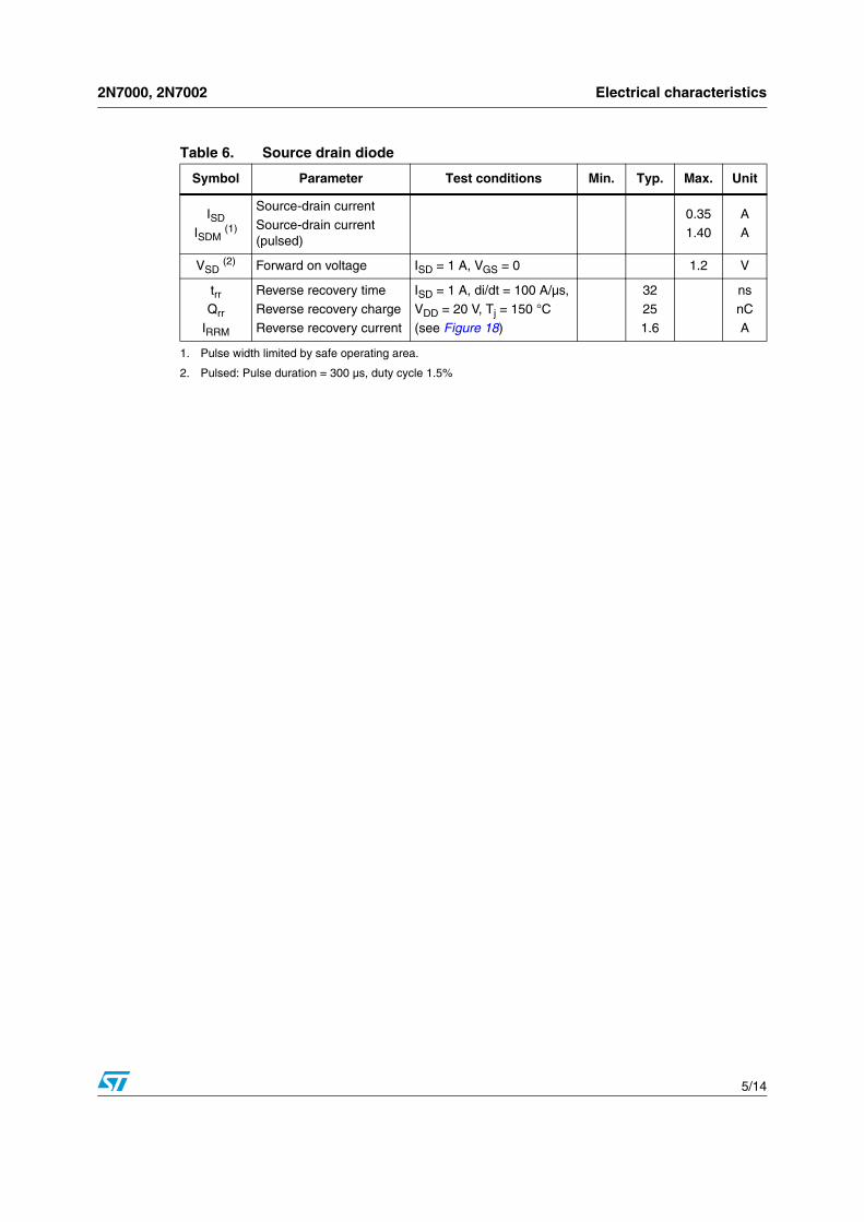
2N7000, 2N7002 Electrical characteristics
5/14
Table 6. Source drain diode
Symbol Parameter Test conditions Min. Typ. Max. Unit
ISD
ISDM (1)
1. Pulse width limited by safe operating area.
Source-drain current
Source-drain current (pulsed)
0.351.40
AA
VSD (2)
2. Pulsed: Pulse duration = 300 µs, duty cycle 1.5%
Forward on voltage ISD = 1 A, VGS = 0 1.2 V
trrQrr
IRRM
Reverse recovery timeReverse recovery charge
Reverse recovery current
ISD = 1 A, di/dt = 100 A/µs,VDD = 20 V, Tj = 150 °C
(see Figure 18)
3225
1.6
nsnC
A
Electrical characteristics 2N7000, 2N7002
6/14
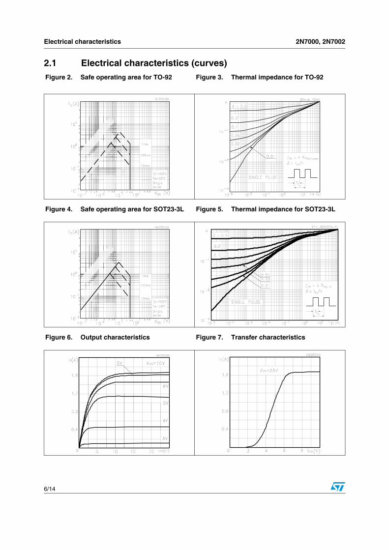
2.1 Electrical characteristics (curves) Figure 2. Safe operating area for TO-92 Figure 3. Thermal impedance for TO-92
Figure 4. Safe operating area for SOT23-3L Figure 5. Thermal impedance for SOT23-3L
Figure 6. Output characteristics Figure 7. Transfer characteristics
2N7000, 2N7002 Electrical characteristics
7/14
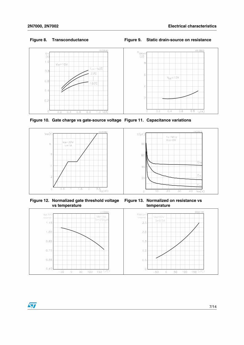
Figure 8. Transconductance Figure 9. Static drain-source on resistance
Figure 10. Gate charge vs gate-source voltage Figure 11. Capacitance variations
Figure 12. Normalized gate threshold voltage vs temperature
Figure 13. Normalized on resistance vs temperature
Electrical characteristics 2N7000, 2N7002
8/14
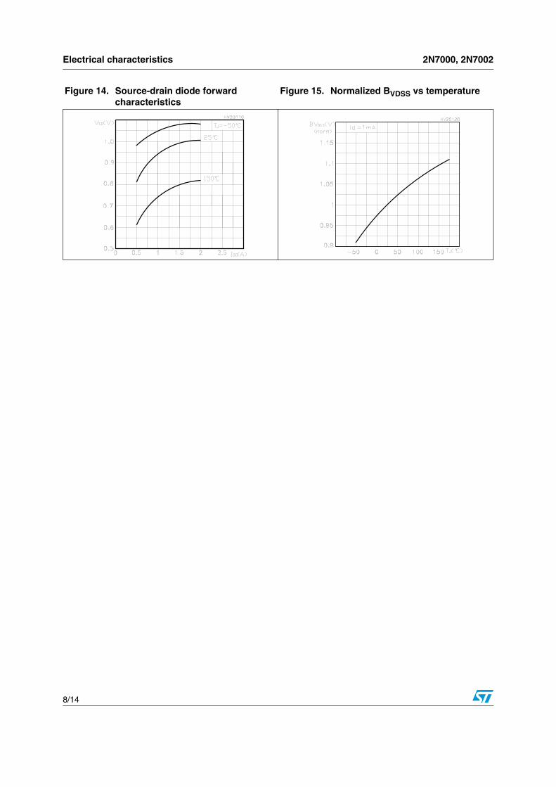
Figure 14. Source-drain diode forward characteristics
Figure 15. Normalized BVDSS vs temperature
2N7000, 2N7002 Test circuits
9/14
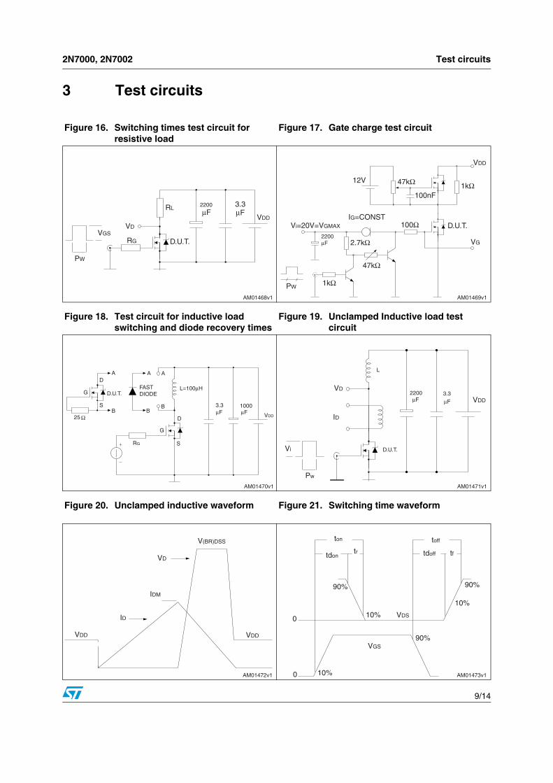
3 Test circuits
Figure 16. Switching times test circuit for resistive load
Figure 17. Gate charge test circuit
Figure 18. Test circuit for inductive load switching and diode recovery times
Figure 19. Unclamped Inductive load test circuit
Figure 20. Unclamped inductive waveform Figure 21. Switching time waveform
AM01468v1
VGS
PW
VD
RG
RL
D.U.T.
2200
µF3.3µF
VDD
AM01469v1
VDD
47kΩ 1kΩ
47kΩ
2.7kΩ
1kΩ
12V
Vi=20V=VGMAX
2200µF
PW
IG=CONST100Ω
100nF
D.U.T.
VG
AM01470v1
AD
D.U.T.
SB
G
25 Ω
A A
BB
RG
G
FASTDIODE
D
S
L=100µH
µF3.3 1000
µF VDD
AM01471v1
Vi
Pw
VD
ID
D.U.T.
L
2200µF
3.3µF VDD
AM01472v1
V(BR)DSS
VDDVDD
VD
IDM
ID
AM01473v1
VDS
ton
tdon tdoff
toff
tftr
90%
10%
10%
0
0
90%
90%
10%
VGS
Package mechanical data 2N7000, 2N7002
10/14
4 Package mechanical data
In order to meet environmental requirements, ST offers these devices in ECOPACK® packages. These packages have a Lead-free second level interconnect. The category of second level interconnect is marked on the package and on the inner box label, in compliance with JEDEC Standard JESD97. The maximum ratings related to soldering conditions are also marked on the inner box label. ECOPACK is an ST trademark. ECOPACK specifications are available at: www.st.com
2N7000, 2N7002 Package mechanical data
11/14
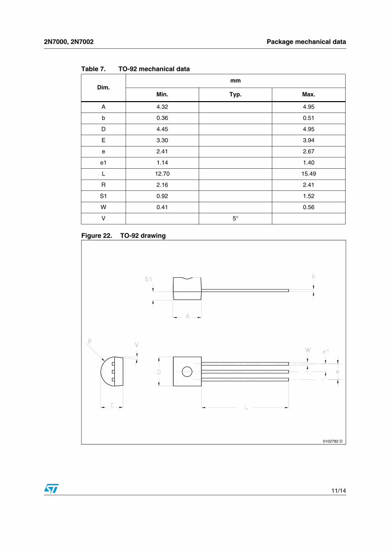
Figure 22. TO-92 drawing
Table 7. TO-92 mechanical data
Dim.mm
Min. Typ. Max.
A 4.32 4.95
b 0.36 0.51
D 4.45 4.95
E 3.30 3.94
e 2.41 2.67
e1 1.14 1.40
L 12.70 15.49
R 2.16 2.41
S1 0.92 1.52
W 0.41 0.56
V 5°
0102782 D

Package mechanical data 2N7000, 2N7002
12/14
Figure 23. SOT23-3L drawing
Table 8. SOT23-3L mechanical data
Dim.mm
Min. Typ. Max.
A 1.25
A1 0 0.15
A2 1.00 1.20
A3 0.60 0.70
D 2.826 3.026
E 2.60 3.00
E1 1.526 1.726
e 0.95
e1 1.90
L 0.35 0.60
L1 0.59
L2 0.25
R 0.05
R1 0.05 0.20
K 3° 7°
K1 6° 10°
Bottom view
Top view
8162275_Rev_A
2N7000, 2N7002 Revision history
13/14
5 Revision history
Table 9. Document revision history
Date Revision Changes
09-Oct-2004 1 First document
22-Jun-2004 2 Complete document
06-Apr-2005 3 New typ and max value inserted for Vgs(th)
19-Apr-2005 4 The document has been reformatted
26-Apr-2005 5 New Pin configuration for TO-92
28-Apr-2005 6 Pin configuration change again
19-Jun-2006 7 New template, no content change
03-Sep-2007 8 Corrected marking on first page
04-Nov-2008 9
– Updated Table 7: TO-92 mechanical data and Figure 22: TO-92 drawing.
– Updated Table 8: SOT23-3L mechanical data and Figure 23: SOT23-3L drawing.
2N7000, 2N7002
14/14
Please Read Carefully:
Information in this document is provided solely in connection with ST products. STMicroelectronics NV and its subsidiaries (“ST”) reserve theright to make changes, corrections, modifications or improvements, to this document, and the products and services described herein at anytime, without notice.
All ST products are sold pursuant to ST’s terms and conditions of sale.
Purchasers are solely responsible for the choice, selection and use of the ST products and services described herein, and ST assumes noliability whatsoever relating to the choice, selection or use of the ST products and services described herein.
No license, express or implied, by estoppel or otherwise, to any intellectual property rights is granted under this document. If any part of thisdocument refers to any third party products or services it shall not be deemed a license grant by ST for the use of such third party productsor services, or any intellectual property contained therein or considered as a warranty covering the use in any manner whatsoever of suchthird party products or services or any intellectual property contained therein.
UNLESS OTHERWISE SET FORTH IN ST’S TERMS AND CONDITIONS OF SALE ST DISCLAIMS ANY EXPRESS OR IMPLIEDWARRANTY WITH RESPECT TO THE USE AND/OR SALE OF ST PRODUCTS INCLUDING WITHOUT LIMITATION IMPLIEDWARRANTIES OF MERCHANTABILITY, FITNESS FOR A PARTICULAR PURPOSE (AND THEIR EQUIVALENTS UNDER THE LAWSOF ANY JURISDICTION), OR INFRINGEMENT OF ANY PATENT, COPYRIGHT OR OTHER INTELLECTUAL PROPERTY RIGHT.
UNLESS EXPRESSLY APPROVED IN WRITING BY AN AUTHORIZED ST REPRESENTATIVE, ST PRODUCTS ARE NOTRECOMMENDED, AUTHORIZED OR WARRANTED FOR USE IN MILITARY, AIR CRAFT, SPACE, LIFE SAVING, OR LIFE SUSTAININGAPPLICATIONS, NOR IN PRODUCTS OR SYSTEMS WHERE FAILURE OR MALFUNCTION MAY RESULT IN PERSONAL INJURY,DEATH, OR SEVERE PROPERTY OR ENVIRONMENTAL DAMAGE. ST PRODUCTS WHICH ARE NOT SPECIFIED AS "AUTOMOTIVEGRADE" MAY ONLY BE USED IN AUTOMOTIVE APPLICATIONS AT USER’S OWN RISK.
Resale of ST products with provisions different from the statements and/or technical features set forth in this document shall immediately voidany warranty granted by ST for the ST product or service described herein and shall not create or extend in any manner whatsoever, anyliability of ST.
ST and the ST logo are trademarks or registered trademarks of ST in various countries.
Information in this document supersedes and replaces all information previously supplied.
The ST logo is a registered trademark of STMicroelectronics. All other names are the property of their respective owners.
© 2008 STMicroelectronics - All rights reserved
STMicroelectronics group of companies
Australia - Belgium - Brazil - Canada - China - Czech Republic - Finland - France - Germany - Hong Kong - India - Israel - Italy - Japan - Malaysia - Malta - Morocco - Singapore - Spain - Sweden - Switzerland - United Kingdom - United States of America
www.st.com