20 + 20W STEREO AMPLIFIER WITH STAND-BY · PDF file20+20w stereo amplifier with stand-by wide...
8
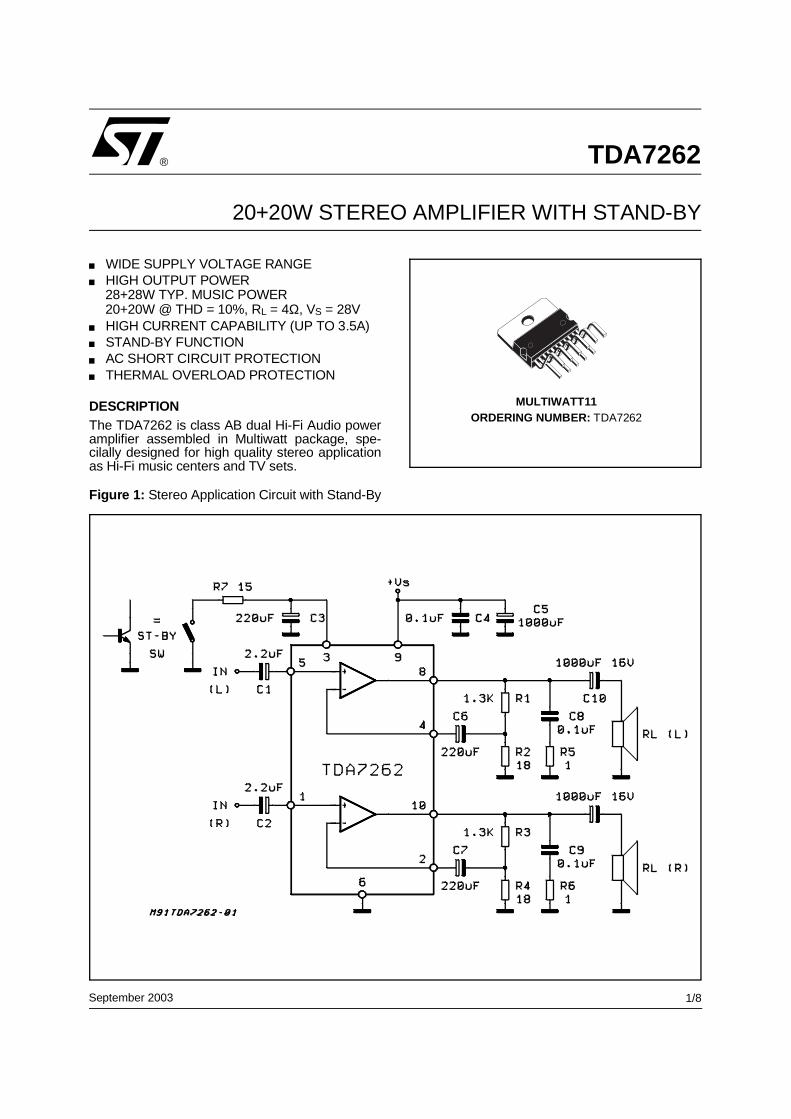
TDA7262 20+20W STEREO AMPLIFIER WITH STAND-BY WIDE SUPPLY VOLTAGE RANGE HIGH OUTPUT POWER 28+28W TYP. MUSIC POWER 20+20W @ THD = 10%, RL = 4Ω, VS = 28V HIGH CURRENT CAPABILITY (UP TO 3.5A) STAND-BY FUNCTION AC SHORT CIRCUIT PROTECTION THERMAL OVERLOAD PROTECTION DESCRIPTION The TDA7262 is class AB dual Hi-Fi Audio power amplifier assembled in Multiwatt package, spe- cilally designed for high quality stereo application as Hi-Fi music centers and TV sets. September 2003 ® Figure 1: Stereo Application Circuit with Stand-By MULTIWATT11 ORDERING NUMBER: TDA7262 1/8
Transcript of 20 + 20W STEREO AMPLIFIER WITH STAND-BY · PDF file20+20w stereo amplifier with stand-by wide...
TDA7262
20+20W STEREO AMPLIFIER WITH STAND-BY
WIDE SUPPLY VOLTAGE RANGEHIGH OUTPUT POWER28+28W TYP. MUSIC POWER20+20W @ THD = 10%, RL = 4Ω, VS = 28VHIGH CURRENT CAPABILITY (UP TO 3.5A)STAND-BY FUNCTIONAC SHORT CIRCUIT PROTECTIONTHERMAL OVERLOAD PROTECTION
DESCRIPTIONThe TDA7262 is class AB dual Hi-Fi Audio poweramplifier assembled in Multiwatt package, spe-cilally designed for high quality stereo applicationas Hi-Fi music centers and TV sets.
September 2003
®
Figure 1: Stereo Application Circuit with Stand-By
MULTIWATT11ORDERING NUMBER: TDA7262
1/8
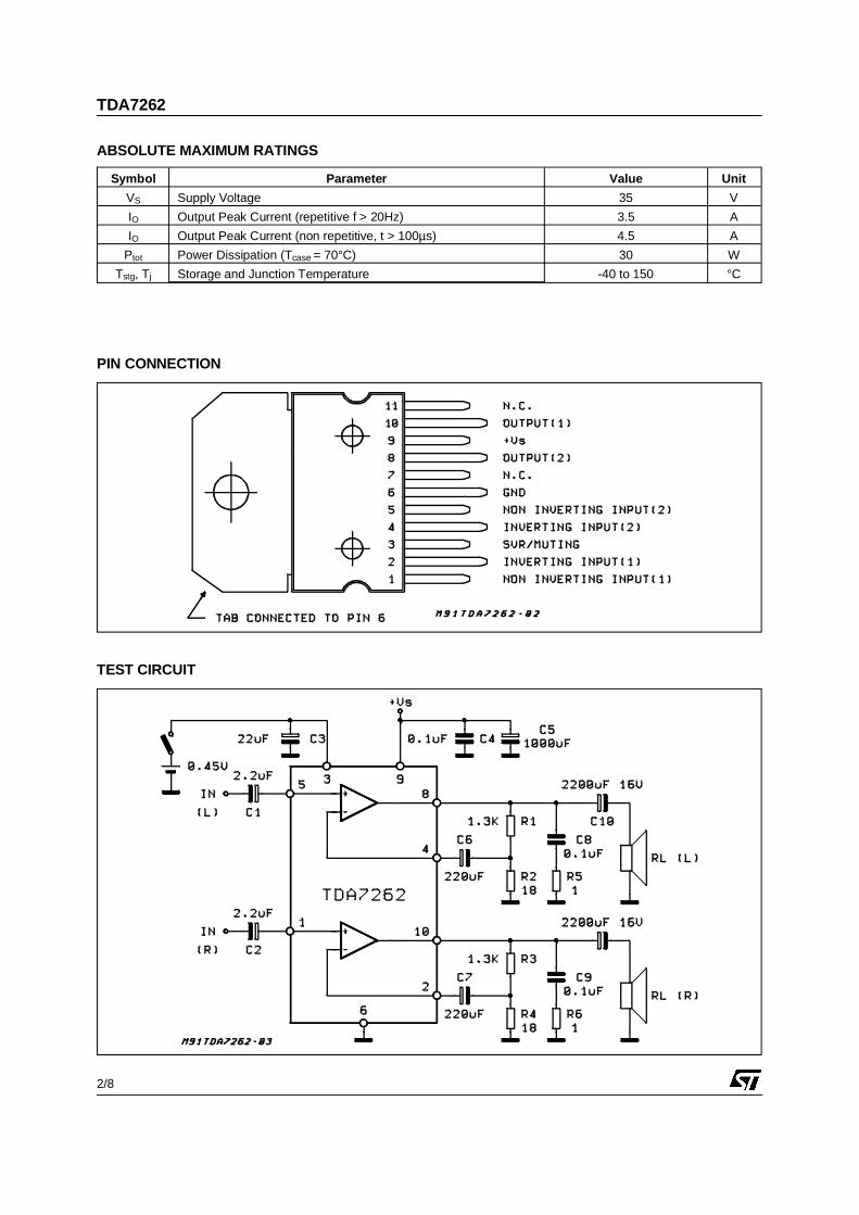
TEST CIRCUIT
ABSOLUTE MAXIMUM RATINGS
Symbol Parameter Value Unit
VS Supply Voltage 35 V
IO Output Peak Current (repetitive f > 20Hz) 3.5 A
IO Output Peak Current (non repetitive, t > 100µs) 4.5 A
Ptot Power Dissipation (Tcase = 70°C) 30 W
Tstg, Tj Storage and Junction Temperature -40 to 150 °C
PIN CONNECTION
TDA7262
2/8
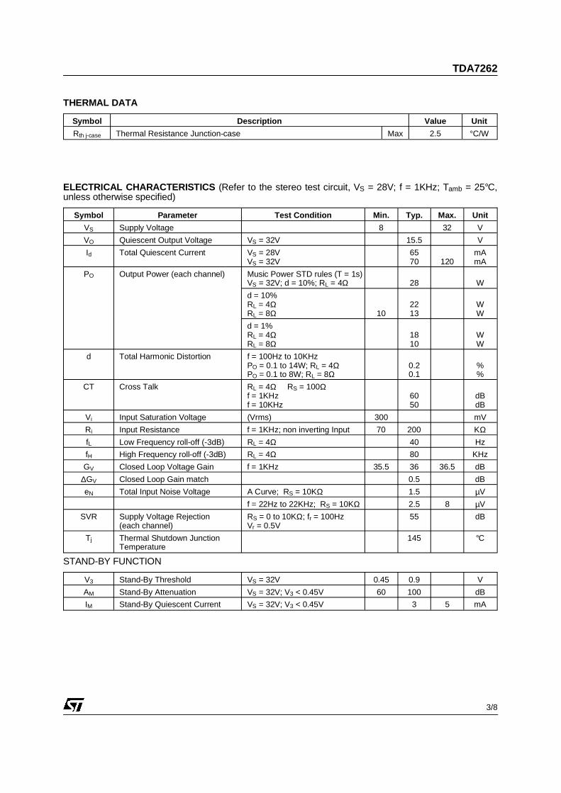
THERMAL DATA
Symbol Description Value Unit
Rth j-case Thermal Resistance Junction-case Max 2.5 °C/W
ELECTRICAL CHARACTERISTICS (Refer to the stereo test circuit, VS = 28V; f = 1KHz; Tamb = 25°C,unless otherwise specified)
Symbol Parameter Test Condition Min. Typ. Max. Unit
VS Supply Voltage 8 32 V
VO Quiescent Output Voltage VS = 32V 15.5 V
Id Total Quiescent Current VS = 28VVS = 32V
6570 120
mAmA
PO Output Power (each channel) Music Power STD rules (T = 1s)VS = 32V; d = 10%; RL = 4Ω 28 W
d = 10%RL = 4ΩRL = 8Ω 10
2213
WW
d = 1%RL = 4ΩRL = 8Ω
1810
WW
d Total Harmonic Distortion f = 100Hz to 10KHzPO = 0.1 to 14W; RL = 4ΩPO = 0.1 to 8W; RL = 8Ω
0.20.1
%%
CT Cross Talk RL = 4Ω RS = 100Ω f = 1KHzf = 10KHz
6050
dBdB
Vi Input Saturation Voltage (Vrms) 300 mV
Ri Input Resistance f = 1KHz; non inverting Input 70 200 KΩfL Low Frequency roll-off (-3dB) RL = 4Ω 40 Hz
fH High Frequency roll-off (-3dB) RL = 4Ω 80 KHz
GV Closed Loop Voltage Gain f = 1KHz 35.5 36 36.5 dB
∆GV Closed Loop Gain match 0.5 dB
eN Total Input Noise Voltage A Curve; RS = 10KΩ 1.5 µV
f = 22Hz to 22KHz; RS = 10KΩ 2.5 8 µV
SVR Supply Voltage Rejection(each channel)
RS = 0 to 10KΩ; fr = 100HzVr = 0.5V
55 dB
Tj Thermal Shutdown JunctionTemperature
145 °C
STAND-BY FUNCTION
V3 Stand-By Threshold VS = 32V 0.45 0.9 V
AM Stand-By Attenuation VS = 32V; V3 < 0.45V 60 100 dB
IM Stand-By Quiescent Current VS = 32V; V3 < 0.45V 3 5 mA
TDA7262
3/8
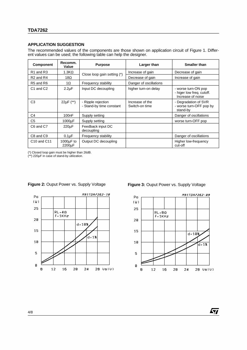
APPLICATION SUGGESTIONThe recommended values of the components are those shown on application circuit of Figure 1. Differ-ent values can be used; the following table can help the designer.
Component Recomm.Value Purpose Larger than Smaller than
R1 and R3 1.3KΩClose loop gain setting (*)
Increase of gain Decrease of gain
R2 and R4 18Ω Decrease of gain Increase of gain
R5 and R6 1Ω Frequency stability Danger of oscillations
C1 and C2 2.2µF Input DC decoupling higher turn-on delay - worse turn-ON pop- higer low freq. cutoff. Increase of noise
C3 22µF (**) - Ripple rejection- Stand-by time constant
Increase of theSwitch-on time
- Degradation of SVR- worse turn-OFF pop by stand-by
C4 100nF Supply setting Danger of oscillations
C5 1000µF Supply setting worse turn-OFF pop
C6 and C7 220µF Feedback input DCdecoupling
C8 and C9 0.1µF Frequency stability Danger of oscillations
C10 and C11 1000µF to2200µF
Output DC decoupling Higher low-frequencycut-off
(*) Closed loop gain must be higher than 26dB.(**) 220µF in case of stand-by utilization.
Figure 2: Ouput Power vs. Supply Voltage Figure 3: Ouput Power vs. Supply Voltage
TDA7262
4/8
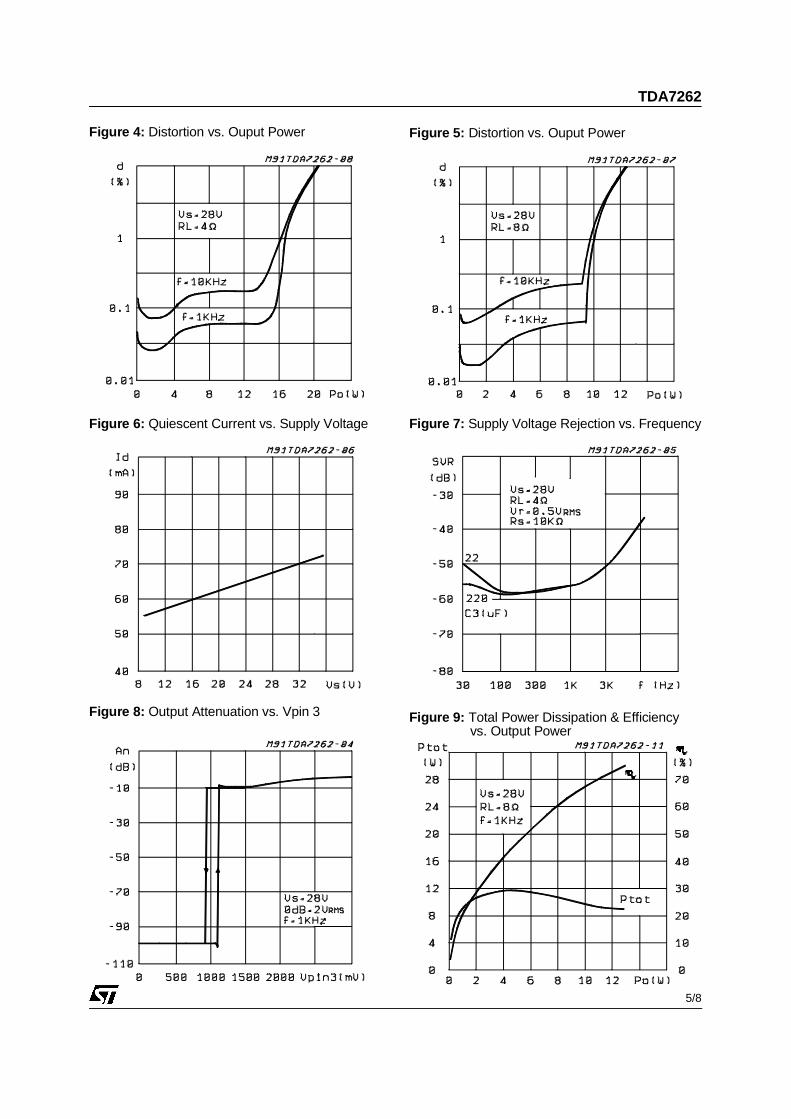
Figure 4: Distortion vs. Ouput Power
Figure 6: Quiescent Current vs. Supply Voltage
Figure 5: Distortion vs. Ouput Power
Figure 7: Supply Voltage Rejection vs. Frequency
Figure 8: Output Attenuation vs. Vpin 3 Figure 9: Total Power Dissipation & Efficiencyvs. Output Power
TDA7262
5/8
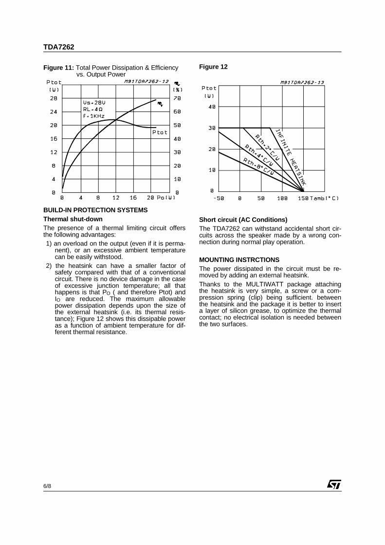
BUILD-IN PROTECTION SYSTEMSThermal shut-downThe presence of a thermal limiting circuit offersthe following advantages:1) an overload on the output (even if it is perma-
nent), or an excessive ambient temperaturecan be easily withstood.
2) the heatsink can have a smaller factor ofsafety compared with that of a conventionalcircuit. There is no device damage in the caseof excessive junction temperature; all thathappens is that PO ( and therefore Ptot) andIO are reduced. The maximum allowablepower dissipation depends upon the size ofthe external heatsink (i.e. its thermal resis-tance); Figure 12 shows this dissipable poweras a function of ambient temperature for dif-ferent thermal resistance.
Short circuit (AC Conditions)The TDA7262 can withstand accidental short cir-cuits across the speaker made by a wrong con-nection during normal play operation.
MOUNTING INSTRCTIONSThe power dissipated in the circuit must be re-moved by adding an external heatsink.Thanks to the MULTIWATT package attachingthe heatsink is very simple, a screw or a com-pression spring (clip) being sufficient. betweenthe heatsink and the package it is better to inserta layer of silicon grease, to optimize the thermalcontact; no electrical isolation is needed betweenthe two surfaces.
Figure 11: Total Power Dissipation & Efficiencyvs. Output Power
Figure 12
TDA7262
6/8
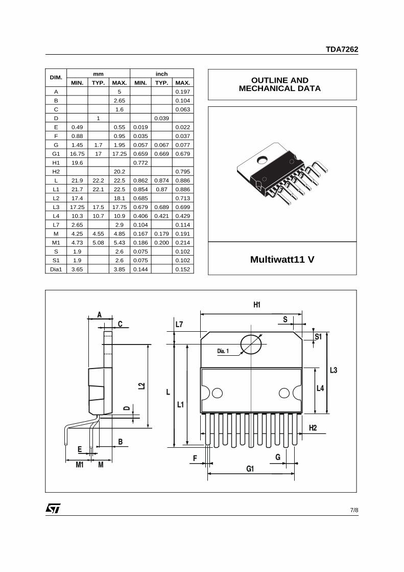
Multiwatt11 V
DIM.mm inch
MIN. TYP. MAX. MIN. TYP. MAX.
A 5 0.197
B 2.65 0.104
C 1.6 0.063
D 1 0.039
E 0.49 0.55 0.019 0.022
F 0.88 0.95 0.035 0.037
G 1.45 1.7 1.95 0.057 0.067 0.077
G1 16.75 17 17.25 0.659 0.669 0.679
H1 19.6 0.772
H2 20.2 0.795
L 21.9 22.2 22.5 0.862 0.874 0.886
L1 21.7 22.1 22.5 0.854 0.87 0.886
L2 17.4 18.1 0.685 0.713
L3 17.25 17.5 17.75 0.679 0.689 0.699
L4 10.3 10.7 10.9 0.406 0.421 0.429
L7 2.65 2.9 0.104 0.114
M 4.25 4.55 4.85 0.167 0.179 0.191
M1 4.73 5.08 5.43 0.186 0.200 0.214
S 1.9 2.6 0.075 0.102
S1 1.9 2.6 0.075 0.102
Dia1 3.65 3.85 0.144 0.152
OUTLINE ANDMECHANICAL DATA
TDA7262
7/8
Information furnished is believed to be accurate and reliable. However, STMicroelectronics assumes no responsibility for the consequencesof use of such information nor for any infringement of patents or other rights of third parties which may result from its use. No license isgranted by implication or otherwise under any patent or patent rights of STMicroelectronics. Specifications mentioned in this publication aresubject to change without notice. This publication supersedes and replaces all information previously supplied. STMicroelectronics productsare not authorized for use as critical components in life support devices or systems without express written approval of STMicroelectronics.
The ST logo is a registered trademark of STMicroelectronics.All other names are the property of their respective owners
© 2003 STMicroelectronics - All rights reserved
STMicroelectronics GROUP OF COMPANIESAustralia – Belgium - Brazil - Canada - China – Czech Republic - Finland - France - Germany - Hong Kong - India - Israel - Italy - Japan -
Malaysia - Malta - Morocco - Singapore - Spain - Sweden - Switzerland - United Kingdom - United Stateswww.st.com
TDA7262
8/8