2 x 1.5W, Stereo Class D Audio Subsystem with … · Maxim’s 3rd-generation, ultra-low-EMI, Class...
38
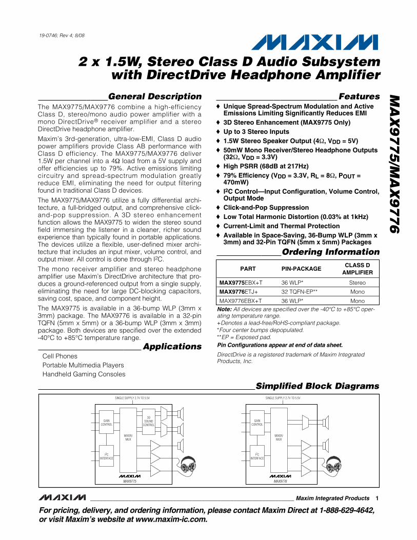
General Description The MAX9775/MAX9776 combine a high-efficiency Class D, stereo/mono audio power amplifier with a mono DirectDrive ® receiver amplifier and a stereo DirectDrive headphone amplifier. Maxim’s 3rd-generation, ultra-low-EMI, Class D audio power amplifiers provide Class AB performance with Class D efficiency. The MAX9775/MAX9776 deliver 1.5W per channel into a 4Ω load from a 5V supply and offer efficiencies up to 79%. Active emissions limiting circuitry and spread-spectrum modulation greatly reduce EMI, eliminating the need for output filtering found in traditional Class D devices. The MAX9775/MAX9776 utilize a fully differential archi- tecture, a full-bridged output, and comprehensive click- and-pop suppression. A 3D stereo enhancement function allows the MAX9775 to widen the stereo sound field immersing the listener in a cleaner, richer sound experience than typically found in portable applications. The devices utilize a flexible, user-defined mixer archi- tecture that includes an input mixer, volume control, and output mixer. All control is done through I 2 C. The mono receiver amplifier and stereo headphone amplifier use Maxim’s DirectDrive architecture that pro- duces a ground-referenced output from a single supply, eliminating the need for large DC-blocking capacitors, saving cost, space, and component height. The MAX9775 is available in a 36-bump WLP (3mm x 3mm) package. The MAX9776 is available in a 32-pin TQFN (5mm x 5mm) or a 36-bump WLP (3mm x 3mm) package. Both devices are specified over the extended -40°C to +85°C temperature range. Applications Cell Phones Portable Multimedia Players Handheld Gaming Consoles Features ♦ Unique Spread-Spectrum Modulation and Active Emissions Limiting Significantly Reduces EMI ♦ 3D Stereo Enhancement (MAX9775 Only) ♦ Up to 3 Stereo Inputs ♦ 1.5W Stereo Speaker Output (4Ω, V DD = 5V) ♦ 50mW Mono Receiver/Stereo Headphone Outputs (32Ω, V DD = 3.3V) ♦ High PSRR (68dB at 217Hz) ♦ 79% Efficiency (V DD = 3.3V, R L = 8Ω, P OUT = 470mW) ♦ I 2 C Control—Input Configuration, Volume Control, Output Mode ♦ Click-and-Pop Suppression ♦ Low Total Harmonic Distortion (0.03% at 1kHz) ♦ Current-Limit and Thermal Protection ♦ Available in Space-Saving, 36-Bump WLP (3mm x 3mm) and 32-Pin TQFN (5mm x 5mm) Packages MAX9775/MAX9776 2 x 1.5W, Stereo Class D Audio Subsystem with DirectDrive Headphone Amplifier ________________________________________________________________ Maxim Integrated Products 1 Ordering Information MAX9775 MIXER/ MUX GAIN CONTROL 3D SOUND CONTROL I 2 C INTERFACE SINGLE SUPPLY 2.7V TO 5.5V MAX9776 MIXER/ MUX GAIN CONTROL I 2 C INTERFACE SINGLE SUPPLY 2.7V TO 5.5V Simplified Block Diagrams 19-0746; Rev 4; 8/08 For pricing, delivery, and ordering information, please contact Maxim Direct at 1-888-629-4642, or visit Maxim’s website at www.maxim-ic.com. Pin Configurations appear at end of data sheet. PART PIN-PACKAGE CLASS D AMPLIFIER MAX9775EBX+T 36 WLP* Stereo MAX9776ETJ+ 32 TQFN-EP** Mono MAX9776EBX+T 36 WLP* Mono Note: All devices are specified over the -40°C to +85°C oper- ating temperature range. +Denotes a lead-free/RoHS-compliant package. *Four center bumps depopulated. **EP = Exposed pad. DirectDrive is a registered trademark of Maxim Integrated Products, Inc.
-
Upload
vuongkhanh -
Category
Documents
-
view
224 -
download
0
Transcript of 2 x 1.5W, Stereo Class D Audio Subsystem with … · Maxim’s 3rd-generation, ultra-low-EMI, Class...
General DescriptionThe MAX9775/MAX9776 combine a high-efficiencyClass D, stereo/mono audio power amplifier with amono DirectDrive® receiver amplifier and a stereoDirectDrive headphone amplifier.
Maxim’s 3rd-generation, ultra-low-EMI, Class D audiopower amplifiers provide Class AB performance withClass D efficiency. The MAX9775/MAX9776 deliver1.5W per channel into a 4Ω load from a 5V supply andoffer efficiencies up to 79%. Active emissions limitingcircuitry and spread-spectrum modulation greatlyreduce EMI, eliminating the need for output filteringfound in traditional Class D devices.
The MAX9775/MAX9776 utilize a fully differential archi-tecture, a full-bridged output, and comprehensive click-and-pop suppression. A 3D stereo enhancementfunction allows the MAX9775 to widen the stereo soundfield immersing the listener in a cleaner, richer soundexperience than typically found in portable applications.The devices utilize a flexible, user-defined mixer archi-tecture that includes an input mixer, volume control, andoutput mixer. All control is done through I2C.
The mono receiver amplifier and stereo headphoneamplifier use Maxim’s DirectDrive architecture that pro-duces a ground-referenced output from a single supply,eliminating the need for large DC-blocking capacitors,saving cost, space, and component height.
The MAX9775 is available in a 36-bump WLP (3mm x3mm) package. The MAX9776 is available in a 32-pinTQFN (5mm x 5mm) or a 36-bump WLP (3mm x 3mm)package. Both devices are specified over the extended-40°C to +85°C temperature range.
ApplicationsCell PhonesPortable Multimedia PlayersHandheld Gaming Consoles
Features♦ Unique Spread-Spectrum Modulation and Active
Emissions Limiting Significantly Reduces EMI♦ 3D Stereo Enhancement (MAX9775 Only)♦ Up to 3 Stereo Inputs♦ 1.5W Stereo Speaker Output (4Ω, VDD = 5V)♦ 50mW Mono Receiver/Stereo Headphone Outputs
(32Ω, VDD = 3.3V)♦ High PSRR (68dB at 217Hz)♦ 79% Efficiency (VDD = 3.3V, RL = 8Ω, POUT =
470mW)♦ I2C Control—Input Configuration, Volume Control,
Output Mode♦ Click-and-Pop Suppression♦ Low Total Harmonic Distortion (0.03% at 1kHz)♦ Current-Limit and Thermal Protection♦ Available in Space-Saving, 36-Bump WLP (3mm x
3mm) and 32-Pin TQFN (5mm x 5mm) Packages
MA
X9
77
5/M
AX
97
76
2 x 1.5W, Stereo Class D Audio Subsystemwith DirectDrive Headphone Amplifier
________________________________________________________________ Maxim Integrated Products 1
Ordering Information
MAX9775
MIXER/MUX
GAINCONTROL
3DSOUND
CONTROL
I2CINTERFACE
SINGLE SUPPLY 2.7V TO 5.5V
MAX9776
MIXER/MUX
GAINCONTROL
I2CINTERFACE
SINGLE SUPPLY 2.7V TO 5.5V
Simplified Block Diagrams
19-0746; Rev 4; 8/08
For pricing, delivery, and ordering information, please contact Maxim Direct at 1-888-629-4642,or visit Maxim’s website at www.maxim-ic.com.
Pin Configurations appear at end of data sheet.
PART PIN-PACKAGECLASS D
AMPLIFIER
MAX9775EBX+T 36 WLP* Stereo
MAX9776ETJ+ 32 TQFN-EP** Mono
MAX9776EBX+T 36 WLP* MonoNote: All devices are specified over the -40°C to +85°C oper-ating temperature range.+Denotes a lead-free/RoHS-compliant package.*Four center bumps depopulated.**EP = Exposed pad.
DirectDrive is a registered trademark of Maxim IntegratedProducts, Inc.
MA
X9
77
5/M
AX
97
76
2 x 1.5W, Stereo Class D Audio Subsystemwith DirectDrive Headphone Amplifier
2 _______________________________________________________________________________________
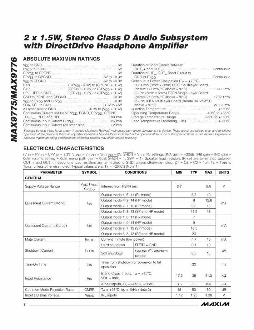
ABSOLUTE MAXIMUM RATINGS
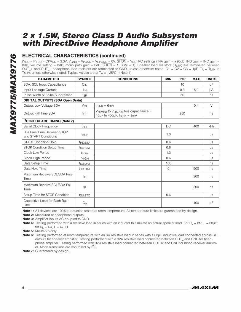
ELECTRICAL CHARACTERISTICS(VDD = PVDD = CPVDD = 3.3V, VGND = VPGND = VCPGND = 0V, SHDN = VDD, I2C settings (INA gain = +20dB, INB gain = INC gain =0dB, volume setting = 0dB, mono path gain = 0dB, SHDN = 1, SSM = 1). Speaker load resistors (RLSP) are terminated betweenOUT_+ and OUT_-, headphone load resistors are terminated to GND, unless otherwise noted. C1 = C2 = C3 = 1µF. TA = TMIN toTMAX, unless otherwise noted. Typical values are at TA = +25°C.) (Note 1)
Stresses beyond those listed under “Absolute Maximum Ratings” may cause permanent damage to the device. These are stress ratings only, and functionaloperation of the device at these or any other conditions beyond those indicated in the operational sections of the specifications is not implied. Exposure toabsolute maximum rating conditions for extended periods may affect device reliability.
VDD to GND..............................................................................6VPVDD to PGND .........................................................................6VCPVDD to CPGND ....................................................................6VCPVSS to CPGND .....................................................-6V to +0.3VVSS to CPGND..........................................................-6V to +0.3VC1N .......................................(CPVSS - 0.3V) to (CPGND + 0.3V)C1P.......................................(CPGND - 0.3V) to (CPVDD + 0.3V)HPL, HPR to GND...................(CPVSS - 0.3V) to (CPVDD + 0.3V)GND to PGND and CPGND................................................±0.3VVDD to PVDD and CPVDD....................................................±0.3VSDA, SCL to GND.....................................................-0.3V to +6VAll other pins to GND..................................-0.3V to (VDD + 0.3V)Continuous Current In/Out of PVDD, PGND, CPVDD, CPGND,OUT__, HPR, and HPL..................................................±800mA
Continuous Input Current CPVSS ......................................260mAContinuous Input Current (all other pins) .........................±20mA
Duration of Short Circuit Between OUT_+ and OUT_- ..................................................Continuous
Duration of HP_, OUT_ Short Circuit to GND or PVDD ..........................................................Continuous
Continuous Power Dissipation (TA = +70°C)36-Bump (3mm x 3mm) UCSP Multilayer Board (derate 17.0mW/°C above +70°C)...........................1360.5mW32-Pin (5mm x 5mm) TQFN Single-Layer Board (derate 21.3mW/°C above +70°C)...........................1702.1mW32-Pin TQFN Multilayer Board (derate 34.5mW/°C above +70°C)...........................................................2758.6mW
Junction Temperature ......................................................+150°COperating Temperature Range ...........................-40°C to +85°CStorage Temperature Range .............................-65°C to +150°CLead Temperature (soldering, 10s) .................................+300°C
PARAMETER SYMBOL CONDITIONS MIN TYP MAX UNITS
GENERAL
Supply Voltage RangeVDD, PVDD,
CPVDDInferred from PSRR test 2.7 5.5 V
Output mode 1, 6, 11 (Rx mode) 6.3 10
Output mode 4, 9, 14 (HP mode) 8 12.6
Output mode 2, 7, 12 (SP mode) 9.5 15Quiescent Current (Mono) IDD
Output mode 3, 8, 13 (SP and HP mode) 12.9 18
mA
Output mode 1, 6, 11 (Rx mode) 7
Output mode 4, 9, 14 (HP mode) 9
Output mode 2, 7, 12 (SP mode) 16.5Quiescent Current (Stereo) IDD
Output mode 3, 8, 13 (SP and HP mode) 20
mA
Mute Current IMUTE Current in mute (low power) 4.7 10 mA
Hard shutdown SHDN = GND 0.1 10
Shutdown Current ISHDNSoft shutdown
See the I2C Interfacesection
8.5 15µA
Turn-On Time tONTime from shutdown or power-on to fulloperation
30 ms
B and C pair inputs, TA = +25°C,VOL = max
17.5 28 41.0 kΩInput Resistance RIN
A pair inputs, TA = +25°C, +20dB 3.5 5.5 8.0 kΩCommon-Mode Rejection Ratio CMRR TA = +25°C, fIN = 1kHz (Note 2) 45 50 60 dB
Input DC Bias Voltage VBIAS IN_ inputs 1.12 1.25 1.38 V

MA
X9
77
5/M
AX
97
76
2 x 1.5W, Stereo Class D Audio Subsystemwith DirectDrive Headphone Amplifier
_______________________________________________________________________________________ 3
PARAMETER SYMBOL CONDITIONS MIN TYP MAX UNITS
SPEAKER AMPLIFIERS
TA = +25°C ±5.5 ±23.5Output Offset Voltage VOS
TMIN ≤ TA ≤ TMAX ±40mV
Into shutdown -62
Out of shutdown -60
Into mute -63Click-and-Pop Level KCP
P eak vol tag e,TA = + 25°C ,A- w ei g hted , 32sam p l es p er second ( N otes 2, 3) Out of mute -62
dB
VDD = 2.7V to 5.5V 48 70
f = 217Hz,100mVP-P ripple
68
f = 1kHz,100mVP-P ripple
60Power-Supply Rejection Ratio(Note 3)
PSRR TA = +25°C
f = 20kHz,100mVP-P ripple
50
dB
RL = 4Ω, VDD = 5V 1500
RL = 8Ω, VDD = 3.3V 450Output Power (Note 4) POUTTHD+N = 1%,TA = +25°C
RL = 8Ω, VDD = 5V 1115
mW
Current Limit 1.6 A
RL = 8Ω,POUT = 125mW
0.03Total Harmonic Distortion PlusNoise (Note 4)
THD+N f = 1kHzRL = 4Ω,POUT = 250mW
0.04
%
BW = 20Hz to 20kHz 81Signal-to-Noise Ratio SNR
VOUT = 1.8VRMS,RL = 8Ω, 3D notactive (Note 3) A-weighted 84
dB
Fixed-frequency modulation 1100Output Frequency fOSC
Spread-spectrum modulation 1100 ± 30kHz
Efficiency η POUT = 470mW, f = 1kHz both channelsdriven, L = 68µH in series with 8Ω load
79 %
Gain AV 12 dB
Channel-to-Channel GainTracking (Note 5)
TA = +25°C ±1 %
3D Sound Resistors (Note 5) R3DUsed with 22nF and 2.2nF externalcapacitors
5 7 9 kΩ
Crosstalk (Notes 4, 5)L to R, R to L, f = 10kHz, RL = 8Ω,VOUT = 300mVRMS
73 dB
ELECTRICAL CHARACTERISTICS (continued)(VDD = PVDD = CPVDD = 3.3V, VGND = VPGND = VCPGND = 0V, SHDN = VDD, I2C settings (INA gain = +20dB, INB gain = INC gain =0dB, volume setting = 0dB, mono path gain = 0dB, SHDN = 1, SSM = 1). Speaker load resistors (RLSP) are terminated betweenOUT_+ and OUT_-, headphone load resistors are terminated to GND, unless otherwise noted. C1 = C2 = C3 = 1µF. TA = TMIN toTMAX, unless otherwise noted. Typical values are at TA = +25°C.) (Note 1)

MA
X9
77
5/M
AX
97
76
2 x 1.5W, Stereo Class D Audio Subsystemwith DirectDrive Headphone Amplifier
4 _______________________________________________________________________________________
ELECTRICAL CHARACTERISTICS (continued)(VDD = PVDD = CPVDD = 3.3V, VGND = VPGND = VCPGND = 0V, SHDN = VDD, I2C settings (INA gain = +20dB, INB gain = INC gain =0dB, volume setting = 0dB, mono path gain = 0dB, SHDN = 1, SSM = 1). Speaker load resistors (RLSP) are terminated betweenOUT_+ and OUT_-, headphone load resistors are terminated to GND, unless otherwise noted. C1 = C2 = C3 = 1µF. TA = TMIN toTMAX, unless otherwise noted. Typical values are at TA = +25°C.) (Note 1)
PARAMETER SYMBOL CONDITIONS MIN TYP MAX UNITS
RECEIVER AMPLIFIER
Output Offset Voltage VOS TA = +25°C ±1.8 ±5.5 mV
Into shutdown -62
Into mute -67
Out of shutdown -63Click-and-Pop Level KCP
Peak voltage, TA =+25°C, A-weighted,32 samples persecond (Notes 3, 6) Out of mute -66
dB
VDD = 2.7V to 5.5V 58 80
f = 217Hz,100mVP-P ripple
80
f = 1kHz,100mVP-P ripple
70Power-Supply Rejection Ratio(Note 3)
PSRR TA = +25°C
f = 20kHz,100mVP-P ripple
62
dB
RL = 16Ω 60Output Power POUT
TA = +25°C,THD+N = 1% RL = 32Ω 50
mW
Gain AV 3 dB
RL = 16Ω (VOUT = 800mVRMS, f = 1kHz) 0.03Total Harmonic Distortion PlusNoise
THD+NRL = 32Ω (VOUT = 800mVRMS, f = 1kHz) 0.024
%
BW = 20Hz to 20kHz 87Signal-to-Noise Ratio SNR
RL = 16Ω, VOUT =800mVRMS (Note 3) A-weighted 89
dB
Slew Rate SR 0.3 V/µs
Capacitive Drive CL 300 pF
HEADPHONE AMPLIFIERS
Output Offset Voltage VOS TA = +25°C ±1.8 ±5.5 mV
Into shutdown -61
Into mute -65
Out of shutdown -60Click-and-Pop Level KCP
Peak voltage, TA =+25°C, A-weighted,32 samples persecond (Notes 2, 4) Out of mute -64
dB
Contact ±4ESD Protection HP_
Air ±8kV
VDD = 2.7V to 5.5V 58 80
f = 217Hz,100mVP-P ripple
80
f = 1kHz,100mVP-P ripple
70Power-Supply Rejection Ratio(Note 3)
PSRR TA = +25°C
f = 20kHz,100mVP-P ripple
62
dB

MA
X9
77
5/M
AX
97
76
2 x 1.5W, Stereo Class D Audio Subsystemwith DirectDrive Headphone Amplifier
_______________________________________________________________________________________ 5
ELECTRICAL CHARACTERISTICS (continued)(VDD = PVDD = CPVDD = 3.3V, VGND = VPGND = VCPGND = 0V, SHDN = VDD, I2C settings (INA gain = +20dB, INB gain = INC gain =0dB, volume setting = 0dB, mono path gain = 0dB, SHDN = 1, SSM = 1). Speaker load resistors (RLSP) are terminated betweenOUT_+ and OUT_-, headphone load resistors are terminated to GND, unless otherwise noted. C1 = C2 = C3 = 1µF. TA = TMIN toTMAX, unless otherwise noted. Typical values are at TA = +25°C.) (Note 1)
PARAMETER SYMBOL CONDITIONS MIN TYP MAX UNITS
RL = 16Ω 60Output Power POUT
TA = +25°C,THD+N = 1% RL = 32Ω 50
mW
Current Limit 170 mA
Gain AV +3 dB
Channel-to-Channel GainTracking
TA = +25°C ±1 %
RL = 16Ω (VOUT = 800mVRMS, f = 1kHz) 0.03Total Harmonic Distortion PlusNoise
THD+NRL = 32Ω (VOUT = 800mVRMS, f = 1kHz) 0.024
%
BW = 20Hz to20kHz
92Signal-to-Noise Ratio SNR
RL = 16Ω,VOUT = 800mVRMS
A-weighted 93
dB
Slew Rate SR 0.3 V/µs
Capacitive Drive CL 300 pF
CrosstalkL to R, R to L, f = 10kHz, RL = 16Ω,VOUT = 160mVRMS
75 dB
VOLUME CONTROL
HP gain (max) 3
SP gain (max) 12
HP gain (min) -72
IN+6dB = 0(minimum gainsetting)
SP gain (min) -63
HP gain (max) 9
SP gain (max) 18
HP gain (min) -61
Volume Control
IN+6dB = 1(maximum gainsetting)
SP gain (min) -57
dB
Mono+6dB = 0 0Mono Gain All outputs
Mono+6dB = 1 6dB
INA+20dB = 0 (minimum gain setting) Set by IN+6dBInput Pair A Control
INA+20dB = 1 (maximum gain setting) 20dB
Mute Attenuation(Minimum Volume)
VIN = 1VRMS 80 dB
DIGITAL INPUTS (SHDN, SDA, SCL)
Input-Voltage High VIH 1.4 V
Input-Voltage Low VIL 0.4 V
Input Hysteresis (SDA, SCL) VHYS 200 mV
MA
X9
77
5/M
AX
97
76
2 x 1.5W, Stereo Class D Audio Subsystemwith DirectDrive Headphone Amplifier
6 _______________________________________________________________________________________
ELECTRICAL CHARACTERISTICS (continued)(VDD = PVDD = CPVDD = 3.3V, VGND = VPGND = VCPGND = 0V, SHDN = VDD, I2C settings (INA gain = +20dB, INB gain = INC gain =0dB, volume setting = 0dB, mono path gain = 0dB, SHDN = 1, SSM = 1). Speaker load resistors (RLSP) are terminated betweenOUT_+ and OUT_-, headphone load resistors are terminated to GND, unless otherwise noted. C1 = C2 = C3 = 1µF. TA = TMIN toTMAX, unless otherwise noted. Typical values are at TA = +25°C.) (Note 1)
PARAMETER SYMBOL CONDITIONS MIN TYP MAX UNITS
SDA, SCL Input Capacitance CIN 10 pF
Input Leakage Current IIN 0.3 5.0 µA
Pulse Width of Spike Suppressed tSP 50 ns
DIGITAL OUTPUTS (SDA Open Drain)
Output Low Voltage SDA VOL ISINK = 6mA 0.4 V
Output Fall Time SDA tOFVH(MIN) to VL(MAX) bus capacitance =10pF to 400pF, ISINK = 3mA
250 ns
I2C INTERFACE TIMING (Note 7)
Serial Clock Frequency fSCL DC 400 kHz
Bus Free Time Between STOPand START Conditions
tBUF 1.3 µs
START Condition Hold tHD:STA 0.6 µs
STOP Condition Setup Time tSU:STA 0.6 µs
Clock Low Period tLOW 1.3 µs
Clock High Period tHIGH 0.6 µs
Data Setup Time tSU:DAT 100 ns
Data Hold Time tHD:DAT 0 900 ns
Maximum Receive SCL/SDA RiseTime
tR 300 ns
Maximum Receive SCL/SDA FallTime
tF 300 ns
Setup Time for STOP Condition tSU:STO 0.6 µs
Capacitive Load for Each BusLine
Cb 400 pF
Note 1: All devices are 100% production tested at room temperature. All temperature limits are guaranteed by design.Note 2: Measured at headphone outputs.Note 3: Amplifier inputs AC-coupled to GND.Note 4: Testing performed with a resistive load in series with an inductor to simulate an actual speaker load. For RL = 8Ω, L = 68µH;
for RL = 4Ω, L = 47µH.Note 5: MAX9775 only.Note 6: Testing performed at room temperature with an 8Ω resistive load in series with a 68µH inductive load connected across BTL
outputs for speaker amplifier. Testing performed with a 32Ω resistive load connected between OUT_ and GND for head-phone amplifier. Testing performed with 32Ω resistive load connected between OUTRx and GND for mono receiver amplifi-er. Mode transitions are controlled by I2C.
Note 7: Guaranteed by design.

MA
X9
77
5/M
AX
97
76
2 x 1.5W, Stereo Class D Audio Subsystemwith DirectDrive Headphone Amplifier
_______________________________________________________________________________________ 7
TOTAL HARMONIC DISTORTION PLUS NOISEvs. FREQUENCY
MAX
9775
/76
toc0
1
FREQUENCY (Hz)
THD+
N (%
)
10k1k100
0.1
0.001
0.01
1
10 100k
VDD = 5VRL = 4Ω
POUT = 400mW
POUT = 1000mW
TOTAL HARMONIC DISTORTION PLUS NOISEvs. FREQUENCY
MAX
9775
/76
toc0
2FREQUENCY (Hz)
THD+
N (%
)
10k1k100
0.1
0.001
0.01
1
10 100k
VDD = 5VRL = 8Ω
POUT = 150mW
POUT = 750mW
TOTAL HARMONIC DISTORTION PLUS NOISEvs. FREQUENCY
MAX
9775
/76
toc0
3
FREQUENCY (Hz)
THD+
N (%
)
10k1k100
0.1
0.001
0.01
1
10 100k
VDD = 3.3VRL = 4Ω
POUT = 400mW
POUT = 150mW
TOTAL HARMONIC DISTORTION PLUS NOISEvs. FREQUENCY
MAX
9775
/76
toc0
4
FREQUENCY (Hz)
THD+
N (%
)
10k1k100
0.1
0.001
0.01
1
10 100k
VDD = 3.3VRL = 8Ω
POUT = 300mW
POUT = 150mW
TOTAL HARMONIC DISTORTION PLUS NOISEvs. FREQUENCY
MAX
9775
/76
toc0
5
FREQUENCY (Hz)
THD+
N (%
)
10k1k100
0.01
0.1
1
0.00110 100k
SSM
FFM
VDD = 3.3VRL = 8ΩPOUT = 500mW
TOTAL HARMONIC DISTORTION PLUS NOISEvs. OUTPUT POWER
MAX
9775
/76
toc0
6
OUTPUT POWER (W)
THD+
N (%
)
1.61.20.80.4
0.01
0.1
1
10
100
0.0010 2.0
VDD = 5VRL = 4Ω
f = 10kHz
f = 20Hz
f = 1kHz
Typical Operating Characteristics(VDD = PVDD = CPVDD = 3.3V, GND = PGND = CPGND = 0V, SHDN = VDD, I2C default gain settings (INA gain = +20dB, INB gain =INC gain = 0dB, volume setting = 0dB, mono path gain = 0dB, SHDN = 1, SSM = 1). Speaker load resistors (RLSP) are terminatedbetween OUT_+ and OUT_-, headphone load resistors are terminated to GND, unless otherwise stated. C1 = C2 = C3 = 1µF. TA =+25°C, unless otherwise noted.)

MA
X9
77
5/M
AX
97
76
2 x 1.5W, Stereo Class D Audio Subsystemwith DirectDrive Headphone Amplifier
8 _______________________________________________________________________________________
Typical Operating Characteristics (continued)(VDD = PVDD = CPVDD = 3.3V, GND = PGND = CPGND = 0V, SHDN = VDD, I2C default gain settings (INA gain = +20dB, INB gain =INC gain = 0dB, volume setting = 0dB, mono path gain = 0dB, SHDN = 1, SSM = 1). Speaker load resistors (RLSP) are terminatedbetween OUT_+ and OUT_-, headphone load resistors are terminated to GND, unless otherwise stated. C1 = C2 = C3 = 1µF. TA =+25°C, unless otherwise noted.)
TOTAL HARMONIC DISTORTION PLUS NOISEvs. OUTPUT POWER
MAX
9775
/76
toc0
7
OUTPUT POWER (W)
THD+
N (%
)
1.20.90.60.3
0.01
0.1
1
10
100
0.0010 1.5
VDD = 5VRL = 8Ω
f = 10kHz
f = 20Hz
f = 1kHz
TOTAL HARMONIC DISTORTION PLUS NOISEvs. OUTPUT POWER
MAX
9775
/76
toc0
8
OUTPUT POWER (W)
THD+
N (%
)
0.60.40.2
0.01
0.1
1
10
100
0.0010 0.8
VDD = 3.3VRL = 4Ω
f = 10kHz
f = 20Hz
f = 1kHz
TOTAL HARMONIC DISTORTION PLUS NOISEvs. OUTPUT POWER
MAX
9775
/76
toc0
9
OUTPUT POWER (W)
THD+
N (%
)
0.40.2
0.01
0.1
1
10
100
0.0010 0.6
VDD = 3.3VRL = 8Ω
f = 10kHz
f = 20Hz
f = 1kHz
TOTAL HARMONIC DISTORTION PLUS NOISEvs. OUTPUT POWER
MAX
9775
/76
toc1
0
OUTPUT POWER (W)
THD+
N (%
)
1.20.90.60.3
0.01
0.1
1
10
100
0.0010 1.5
VDD = 5VRL = 8Ωf = 1kHz
SSM
FFM
EFFICIENCYvs. OUTPUT POWER
MAX
9775
/76
toc1
1
OUTPUT POWER (W)
EFFI
CIEN
CY (%
)
3.22.41.60.8
10
20
30
40
50
60
70
80
90
100
00 4.0
VDD = 5VfIN = 1kHzPOUT = POUTL + POUTR
RL = 8Ω
RL = 4Ω
EFFICIENCYvs. OUTPUT POWER
MAX
9775
/76
toc1
2
OUTPUT POWER (W)
EFFI
CIEN
CY (%
)
1.61.20.80.4
10
20
30
40
50
60
70
80
90
100
00 2.0
VDD = 3.3VfIN = 1kHzPOUT = POUTL + POUTR
RL = 8Ω
RL = 4Ω

MA
X9
77
5/M
AX
97
76
2 x 1.5W, Stereo Class D Audio Subsystemwith DirectDrive Headphone Amplifier
_______________________________________________________________________________________ 9
Typical Operating Characteristics (continued)(VDD = PVDD = CPVDD = 3.3V, GND = PGND = CPGND = 0V, SHDN = VDD, I2C default gain settings (INA gain = +20dB, INB gain =INC gain = 0dB, volume setting = 0dB, mono path gain = 0dB, SHDN = 1, SSM = 1). Speaker load resistors (RLSP) are terminatedbetween OUT_+ and OUT_-, headphone load resistors are terminated to GND, unless otherwise stated. C1 = C2 = C3 = 1µF. TA =+25°C, unless otherwise noted.)
OUTPUT POWERvs. SUPPLY VOLTAGE
MAX
9775
/76
toc1
3
SUPPLY VOLTAGE (V)
OUTP
UT P
OWER
(mW
)
5.24.74.23.73.2
200
400
600
800
1000
1200
1400
1600
1800
2000
2200
02.7
RL = 4Ωf = 1kHz
THD+N = 10%
THD+N = 1%
OUTPUT POWERvs. SUPPLY VOLTAGE
MAX
9775
/76
toc1
4
SUPPLY VOLTAGE (V)
OUTP
UT P
OWER
(mW
)
5.24.73.2 3.7 4.2
200
400
600
800
1000
1200
1400
1600
02.7
RL = 8Ωf = 1kHz
THD+N = 10%
THD+N = 1%
OUTPUT POWERvs. LOAD
MAX
9775
/76
toc1
5
LOAD (Ω)
OUTP
UT P
OWER
(W)
10
0.5
1.0
1.5
2.0
2.5
01 100
THD+N = 10%
THD+N = 1%
VDD = 5Vf = 1kHz
OUTPUT POWERvs. LOAD
MAX
9775
/76
toc1
6
LOAD (Ω)
OUTP
UT P
OWER
(W)
10
200
400
600
800
1000
01 100
THD+N = 10%
THD+N = 1%
VDD = 3.3Vf = 1kHz
POWER-SUPPLY REJECTION RATIOvs. FREQUENCY
MAX
9775
/76
toc1
7
FREQUENCY (Hz)
POW
ER-S
UPPL
Y RE
JECT
ION
RATI
O (d
B)
10k1k100
-90
-80
-70
-60
-50
-40
-30
-20
-10
0
-10010 100k
OUTR
OUTL
VDD = 3.3VVIN = 100mVP-PRL = 8Ω
CROSSTALK vs. FREQUENCY
FREQUENCY (Hz)
CROS
STAL
K (d
B)
MAX
9775
/6 to
c18
-120-110-100-90-80-70-60-50-40-30-20-10
0
10 100 1k 10k 100k
LEFT TO RIGHT
RIGHT TO LEFT
OUT_ = 1VP-PRL = 8Ω

MA
X9
77
5/M
AX
97
76
2 x 1.5W, Stereo Class D Audio Subsystemwith DirectDrive Headphone Amplifier
10 ______________________________________________________________________________________
Typical Operating Characteristics (continued)(VDD = PVDD = CPVDD = 3.3V, GND = PGND = CPGND = 0V, SHDN = VDD, I2C default gain settings (INA gain = +20dB, INB gain =INC gain = 0dB, volume setting = 0dB, mono path gain = 0dB, SHDN = 1, SSM = 1). Speaker load resistors (RLSP) are terminatedbetween OUT_+ and OUT_-, headphone load resistors are terminated to GND, unless otherwise stated. C1 = C2 = C3 = 1µF. TA =+25°C, unless otherwise noted.)
CROSSTALK vs. INPUT AMPLITUDE
INPUT AMPLITUDE (VRMS)
CROS
STAL
K (d
B)
MAX
9775
/6 to
c19
0 0.1 0.2 0.3 0.4 0.5 0.6-120-110-100-90-80-70-60-50-40-30-20-10
0fIN = 1kHzRL = 8ΩGAIN = +12dB
LEFT TO RIGHT
RIGHT TO LEFT
IN-BAND OUTPUT SPECTRUM
MAX
9775
/76
toc2
0
FREQUENCY (Hz)
OUTP
UT M
AGNI
TUDE
(dBV
)
15k10k5k
-120
-100
-80
-60
-40
-20
0
20
-1400 20k
SSM MODERL = 8ΩVDD = 3.3VfIN = 1kHzUNWEIGHTED
IN-BAND OUTPUT SPECTRUM
MAX
9775
/76
toc2
1
FREQUENCY (Hz)
OUTP
UT M
AGNI
TUDE
(dBV
)
15k10k5k
-120
-100
-80
-60
-40
-20
0
20
-1400 20k
FFM MODERL = 8ΩVDD = 3.3VfIN = 1kHzUNWEIGHTED
WIDEBAND OUTPUT SPECTRUMFIXED-FREQUENCY MODE
FREQUENCY (MHz)
OUTP
UT M
AGNI
TUDE
(dBV
) MAX
9775
/6 to
c22
-140
-120
-100
-80
-60
-40
-20
0
20
0.1 1 10 100 1000
VDD = 5VRL = 8ΩINPUTS AC GROUNDED
WIDEBAND OUTPUT SPECTRUMSPREAD-SPECTRUM MODE
FREQUENCY (MHz)
OUTP
UT M
AGNI
TUDE
(dBV
) MAX
9775
toc2
3
-140
-120
-100
-80
-60
-40
-20
0
20
0.1 1 10 100 1000
VDD = 5VRL = 8ΩINPUTS AC GROUNDED
MAX9775 SUPPLY CURRENTvs. SUPPLY VOLTAGE
MAX
9775
/76
toc2
4
SUPPLY VOLTAGE (V)
SUPP
LY C
URRE
NT (m
A)
5.24.74.23.73.2
15
20
25
102.7
SP MODEINPUTS AC GROUNDEDOUTPUTS UNLOADED

MA
X9
77
5/M
AX
97
76
2 x 1.5W, Stereo Class D Audio Subsystemwith DirectDrive Headphone Amplifier
______________________________________________________________________________________ 11
Typical Operating Characteristics (continued)(VDD = PVDD = CPVDD = 3.3V, GND = PGND = CPGND = 0V, SHDN = VDD, I2C default gain settings (INA gain = +20dB, INB gain =INC gain = 0dB, volume setting = 0dB, mono path gain = 0dB, SHDN = 1, SSM = 1). Speaker load resistors (RLSP) are terminatedbetween OUT_+ and OUT_-, headphone load resistors are terminated to GND, unless otherwise stated. C1 = C2 = C3 = 1µF. TA =+25°C, unless otherwise noted.)
MAX9776 SUPPLY CURRENTvs. SUPPLY VOLTAGE
MAX
9775
/76
toc2
5
SUPPLY VOLTAGE (V)
SUPP
LY C
URRE
NT (m
A)
5.24.74.23.73.2
6
8
10
12
14
16
42.7
SP MODEINPUTS AC GROUNDEDOUTPUTS UNLOADED
SHUTDOWN SUPPLY CURRENTvs. SUPPLY VOLTAGE
MAX
9775
/76
toc2
6
SUPPLY VOLTAGE (V)
SUPP
LY C
URRE
NT (n
A)
5.24.74.23.73.2
10
20
30
40
50
60
70
80
90
100
02.7
TOTAL HARMONIC DISTORTION PLUS NOISEvs. FREQUENCY
MAX
9775
/76
toc2
7
FREQUENCY (Hz)
THD+
N (%
)
10k1k100
0.01
0.1
1
0.00110 100k
VDD = 5VRL = 32Ω
POUT = 20mW
POUT = 40mW
TOTAL HARMONIC DISTORTION PLUS NOISEvs. FREQUENCY
MAX
9775
/76
toc2
8
FREQUENCY (Hz)
THD+
N (%
)
10k1k100
0.01
0.1
1
0.00110 100k
VDD = 3.3VRL = 16Ω
POUT = 20mW
POUT = 40mW
TOTAL HARMONIC DISTORTION PLUS NOISEvs. FREQUENCY
MAX
9775
/76
toc2
9
FREQUENCY (Hz)
THD+
N (%
)
10k1k100
0.01
0.1
1
0.00110 100k
VDD = 3.3VRL = 32Ω
POUT = 10mW
POUT = 40mW
TOTAL HARMONIC DISTORTION PLUS NOISEvs. OUTPUT POWER
MAX
9775
/76
toc3
0
OUTPUT POWER (mW)
THD+
N (%
)
604020
0.01
0.1
1
10
100
0.0010 80
VDD = 5VRL = 32Ω
f = 10kHz
f = 20Hz
f = 1kHz

MA
X9
77
5/M
AX
97
76
2 x 1.5W, Stereo Class D Audio Subsystemwith DirectDrive Headphone Amplifier
12 ______________________________________________________________________________________
Typical Operating Characteristics (continued)(VDD = PVDD = CPVDD = 3.3V, GND = PGND = CPGND = 0V, SHDN = VDD, I2C default gain settings (INA gain = +20dB, INB gain =INC gain = 0dB, volume setting = 0dB, mono path gain = 0dB, SHDN = 1, SSM = 1). Speaker load resistors (RLSP) are terminatedbetween OUT_+ and OUT_-, headphone load resistors are terminated to GND, unless otherwise stated. C1 = C2 = C3 = 1µF. TA =+25°C, unless otherwise noted.)
TOTAL HARMONIC DISTORTION PLUS NOISEvs. OUTPUT POWER
OUTPUT POWER (mW)
THD+
N (%
)
MAX
9775
toc3
1
0 30 60 90 1200.001
0.01
0.1
1
10
100
f = 20Hz
f = 1kHz
f = 10kHz
VDD = 3.3VRL = 16Ω
TOTAL HARMONIC DISTORTION PLUS NOISEvs. OUTPUT POWER
MAX
9775
/76
toc3
2
OUTPUT POWER (mW)
THD+
N (%
)
604020
0.01
0.1
1
10
100
0.0010 80
VDD = 3.3VRL = 32Ω
f = 10kHz
f = 20Hz
f = 1kHz
TOTAL HARMONIC DISTORTION PLUS NOISEvs. COMMON-MODE VOLTAGE
COMMON-MODE VOLTAGE (V)
THD+
N (%
)
MAX
9775
/6 to
c33
0 0.5 1.0 1.5 2.0 2.50.001
0.01
0.1
1
10
100VDD = 3.3VfIN = 1kHzPOUT = 30mWGAIN = +3dBRL = 32Ω
POWER DISSIPATIONvs. OUTPUT POWER
MAX
9775
/76
toc3
4
TOTAL OUTPUT POWER (mW)
POW
ER D
ISSI
PATI
ON (m
W)
8040
50
100
150
200
250
300
350
400
450
500
00 120
VDD = 5Vf = 1kHzRL = 32ΩPOUT = POUTR + POUTL
POWER DISSIPATIONvs. OUTPUT POWER
MAX
9775
/76
toc3
5
TOTAL OUTPUT POWER (mW)
POW
ER D
ISSI
PATI
ON (m
W)
1208040
50
100
150
200
250
300
350
400
450
500
00 160
VDD = 3.3Vf = 1kHzPOUT = POUTR + POUTL
RL = 16Ω
RL = 32Ω
OUTPUT POWERvs. SUPPLY VOLTAGE
MAX
9775
/76
toc3
6
SUPPLY VOLTAGE (V)
OUTP
UT P
OWER
(mW
)
5.24.74.23.73.2
35
40
45
50
55
60
65
302.7
THD+N = 10%
THD+N = 1%
RL = 32Ωf = 1kHz

MA
X9
77
5/M
AX
97
76
2 x 1.5W, Stereo Class D Audio Subsystemwith DirectDrive Headphone Amplifier
______________________________________________________________________________________ 13
Typical Operating Characteristics (continued)(VDD = PVDD = CPVDD = 3.3V, GND = PGND = CPGND = 0V, SHDN = VDD, I2C default gain settings (INA gain = +20dB, INB gain =INC gain = 0dB, volume setting = 0dB, mono path gain = 0dB, SHDN = 1, SSM = 1). Speaker load resistors (RLSP) are terminatedbetween OUT_+ and OUT_-, headphone load resistors are terminated to GND, unless otherwise stated. C1 = C2 = C3 = 1µF. TA =+25°C, unless otherwise noted.)
OUTPUT POWERvs. LOAD
MAX
9775
/76
toc3
7
LOAD (Ω)
OUTP
UT P
OWER
(mW
)
100
20
40
60
80
100
120
140
160
180
200
010 1000
THD+N = 10%
THD+N = 1%VDD = 5Vf = 1kHz
OUTPUT POWERvs. LOAD
MAX
9775
/76
toc3
8
LOAD (Ω)
OUTP
UT P
OWER
(mW
)
100
20
40
60
80
100
120
140
160
180
200
010 1000
THD+N = 10%
THD+N = 1%
VDD = 3.3Vf = 1kHz
OUTPUT POWER vs. LOAD RESISTANCEAND CHARGE-PUMP CAPACITOR SIZE
LOAD (Ω)
OUTP
UT P
OWER
(mW
)
MAX
9775
/6 to
c39
0
20
40
60
80
100
10 100 1000
C1 = C2 = 2.2μF
VDD = 3.3Vf = 1kHzTHD+N = 1%
C1 = C2 = 1μF
C1 = C2 = 0.68μF
POWER-SUPPLY REJECTION RATIOvs. FREQUENCY
FREQUENCY (Hz)
POW
ER-S
UPPL
Y RE
JECT
ION
RATI
O (d
B)
MAX
9775
/6 to
c40
-100
-90
-80
-70
-60
-50
-40
-30
-20
-10
0
10 100 1k 10k 100k
HPL
HPR
VDD = 3.3VVIN = 100mVP-PRL = 32Ω
OUTPUT FREQUENCY SPECTRUM
MAX
9775
/76
toc4
1
FREQUENCY (Hz)
OUTP
UT M
AGNI
TUDE
(dBV
)
15k10k5k
-120
-100
-80
-60
-40
-20
0
20
-1400 20k
VDD = 3.3Vf = 1kHzRL = 32Ω
CROSSTALK vs. FREQUENCY
FREQUENCY (Hz)
CROS
STAL
K (d
B)
MAX
9775
/6 to
c42
-120-110-100-90-80-70-60-50-40-30-20-10
0
10 100 1k 10k 100k
OUT_ = 1VP-PRL = 32Ω
LEFT TO RIGHT
RIGHT TO LEFT

MA
X9
77
5/M
AX
97
76
2 x 1.5W, Stereo Class D Audio Subsystemwith DirectDrive Headphone Amplifier
14 ______________________________________________________________________________________
Typical Operating Characteristics (continued)(VDD = PVDD = CPVDD = 3.3V, GND = PGND = CPGND = 0V, SHDN = VDD, I2C default gain settings (INA gain = +20dB, INB gain =INC gain = 0dB, volume setting = 0dB, mono path gain = 0dB, SHDN = 1, SSM = 1). Speaker load resistors (RLSP) are terminatedbetween OUT_+ and OUT_-, headphone load resistors are terminated to GND, unless otherwise stated. C1 = C2 = C3 = 1µF. TA =+25°C, unless otherwise noted.)
CROSSTALK vs. INPUT AMPLITUDE
INPUT AMPLITUDE (VRMS)
CROS
STAL
K (d
B)
MAX
9775
toc4
3
0 0.4 0.8 1.2-120-110-100-90-80-70-60-50-40-30-20-10
0fIN = 1kHzRL = 32ΩGAIN = +3dB
LEFT TO RIGHT
RIGHT TO LEFT
TURN-ON RESPONSEMAX9775/76 toc44
10ms/div
SCL2V/div
SPEAKER OUTPUT50mA/div
HEADPHONEOUTPUT2V/div
TURN-OFF RESPONSEMAX9775/76 toc45
10ms/div
SCL2V/div
SPEAKER OUTPUT50mA/div
HEADPHONEOUTPUT2V/div
MUTE-ON RESPONSEMAX9775/76 toc46
10ms/div
SCL2V/div
SPEAKER OUTPUT50mA/div
HEADPHONEOUTPUT2V/div
MUTE-OFF RESPONSEMAX9775/76 toc47
10ms/div
SCL2V/div
SPEAKER OUTPUT50mA/div
HEADPHONEOUTPUT2V/div
MA
X9
77
5/M
AX
97
76
2 x 1.5W, Stereo Class D Audio Subsystemwith DirectDrive Headphone Amplifier
______________________________________________________________________________________ 15
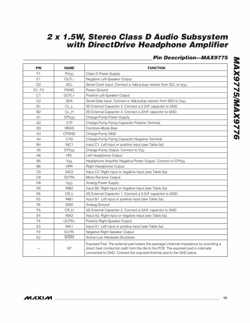
Pin Description—MAX9775
PIN NAME FUNCTION
F1 PVDD Class D Power Supply
E1 OUTL- Negative Left-Speaker Output
D2 SCL Serial Clock Input. Connect a 1kΩ pullup resistor from SCL to VDD.
D1, F3 PGND Power Ground
C1 OUTL+ Positive Left-Speaker Output
C2 SDA Serial Data Input. Connect a 1kΩ pullup resistor from SDA to VDD.
B1 CL_L 3D External Capacitor 3. Connect a 2.2nF capacitor to GND.
B2 CL_H 3D External Capacitor 4. Connect a 22nF capacitor to GND.
A1 CPVDD Charge-Pump Power Supply
A2 C1P Charge-Pump Flying Capacitor Positive Terminal
B3 VBIAS Common-Mode Bias
A3 CPGND Charge-Pump GND
A4 C1N Charge-Pump Flying Capacitor Negative Terminal
B4 INC1 Input C1. Left input or positive input (see Table 5a).
A5 CPVSS Charge-Pump Output. Connect to VSS.
A6 HPL Left Headphone Output
B5 VSS Headphone Amplifier Negative Power Supply. Connect to CPVSS.
B6 HPR Right Headphone Output
C5 INC2 Input C2. Right input or negative input (see Table 5a).
C6 OUTRx Mono Receiver Output
D6 VDD Analog Power Supply
D5 INB2 Input B2. Right input or negative input (see Table 5a).
E6 CR_L 3D External Capacitor 1. Connect a 2.2nF capacitor to GND.
E5 INB1 Input B1. Left input or positive input (see Table 5a).
F6 GND Analog Ground
F5 CR_H 3D External Capacitor 2. Connect a 22nF capacitor to GND.
E4 INA2 Input A2. Right input or negative input (see Table 5a).
F4 OUTR+ Positive Right Speaker Output
E3 INA1 Input A1. Left input or positive input (see Table 5a).
F2 OUTR- Negative Right Speaker Output
E2 SHDN Active-Low Hardware Shutdown
— EPExposed Pad. The external pad lowers the package’s thermal impedance by providing adirect heat conduction path from the die to the PCB. The exposed pad is internallyconnected to GND. Connect the exposed thermal pad to the GND plane.

MA
X9
77
5/M
AX
97
76
2 x 1.5W, Stereo Class D Audio Subsystemwith DirectDrive Headphone Amplifier
16 ______________________________________________________________________________________
Pin Description—MAX9776
PIN
TQFN UCSPNAME FUNCTION
1 F1 PVDD Class D Power Supply
2 E1 OUT- Negative Left-Speaker Output
3 D2 SCL Serial Clock Input. Connect a 1kΩ pullup resistor from SCL to VDD.
4, 29 D1, F3 PGND Power Ground
5 C1 OUT+ Positive Left-Speaker Output
6 C2 SDA Serial Data Input. Connect a 1kΩ pullup resistor from SDA to VDD.
7, 8, 23,26, 28, 31
B1, B2,E6, F2,F4, F5
I.C.Internal Connection. Leave unconnected. This pin is internally connected to the signal path.Do not connect together or to any other pin.
9 A1 CPVDD Charge-Pump Power Supply
10 A2 C1P Charge-Pump Flying Capacitor Positive Terminal
11 B3 VBIAS Common-Mode Bias
12 A3 CPGND Charge-Pump GND
13 A4 C1N Charge-Pump Flying Capacitor Negative Terminal
14 B4 INC1 Input C1. Left input or positive input (see Table 5a).
15 A5 CPVSS Charge-Pump Output. Connect to VSS.
16 A6 HPL Left Headphone Output
17 B5 VSS Headphone Amplifier Negative Power Supply. Connect to CPVSS.
18 B6 HPR Right Headphone Output
19 C5 INC2 Input C2. Right input or negative input (see Table 5a).
20 C6 OUTRx Mono Receiver Output
21 D6 VDD Analog Power Supply
22 D5 INB2 Input B2. Right input or negative input (see Table 5a).
24 E5 INB1 Input B1. Left input or positive input (see Table 5a).
25 F6 GND Analog Ground
27 E4 INA2 Input A2. Right input or negative input (see Table 5a).
30 E3 INA1 Input A1. Left input or positive input (see Table 5a).
32 E2 SHDN Active-Low Hardware Shutdown
EP — EPExposed Pad. The external pad lowers the package’s thermal impedance by providing adirect heat conduction path from the die to the PCB. The exposed pad is internally connectedto GND. Connect the exposed thermal pad to the GND plane.

MA
X9
77
5/M
AX
97
76
2 x 1.5W, Stereo Class D Audio Subsystemwith DirectDrive Headphone Amplifier
______________________________________________________________________________________ 17
Typical Application Circuits
MAX9775
CHARGEPUMP
VDD
C11μF
10kΩ
C31μF
13 (A4)
12 (A3)
10 (A2)
9 (A1)
C1N
VBIAS
CPGND
INPUT A: 0dB,6dB, OR 20dB
C1P
30 (E3)
27 (E4)
1μF
1μF
CPVDD
1μF
6 (C2)
3 (D2)
INA2
INA1
INPUT B: 0dBOR 6dB
MAXIM 3DSOUND
24 (E5)
22 (D5)
1μF
1μF
INB2
INB1
CLASS DAMPLIFIER
INPUT C: 0dBOR 6dB
14 (B4)
19 (C5)
1μF
1μF
INC2
INC1
INPUTMIXER
OUTPUTMIXER
RIGHTVOLUME
LEFTVOLUME
MONOVOLUME
11 (B3)
32 (E2)
SDA
SCL
SHDN
I2C CONTROL
3dB
3dB
3dB
DirectDrive
12dB
CLASS DAMPLIFIER
12dB
OUTR-
OUTRx
HPR
OUTR+
CL_H22nF
OUTL-
OUTL+
HPL
31 (F2)
20 (C6)
18 (B6)
28 (F4)
2 (E1)
5 (C1)
16 (A6)
3D CIRCUIT
8 (B2)
CL_L2.2nF
7 (B1)
CR_H22nF
26 (F5)
CR_L2.2nF
23 (E6)25 (F6)
GND
4 (D1) 29 (F3)
PGNDPGND
C21μF
15 (A5) 17 (B5)
CPVSS VSS
1μF
21 (D6)
VDD
VDD
1μF0.1μF
1 (F1)
PVDD
VDD

MA
X9
77
5/M
AX
97
76
2 x 1.5W, Stereo Class D Audio Subsystemwith DirectDrive Headphone Amplifier
18 ______________________________________________________________________________________
Typical Application Circuits (continued)
MAX9776
CHARGEPUMP
VDD
C11μF
C31μF
13 (A4)
12 (A3)
10 (A2)
9 (A1)
C1N
VBIAS
CPGND
INPUT A: 0dB,6dB, OR 20dB
C1P
30 (E3)
27 (E4)
1μF
1μF
CPVDD
1μF
6 (C2)
3 (D2)
INA2
INA1
INPUT B: 0dBOR 6dB
24 (E5)
22 (D5)
1μF
1μF
INB2
INB1
CLASS DAMPLIFIER
INPUT C: 0dBOR 6dB
14 (B4)
19 (C5)
1μF
1μF
INC2
INC1
INPUTMIXER
OUTPUTMIXER
RIGHTVOLUME
LEFTVOLUME
MONOVOLUME
11 (B3)
32 (E2)
SDA
SCL
SHDN
I2C CONTROL
3dB
3dB
3dB
DirectDrive
12dB
OUTRx
HPR
OUT-
OUT+
HPL
20 (C6)
18 (B6)
2 (E1)
5 (C1)
16 (A6)
25 (F6)
GND
4 (D1) 29 (F3)
PGNDPGND
C21μF
15 (A5) 17 (B5)
CPVSS VSS
1μF
21 (D6)
VDD
VDD
1μF0.1μF
1 (F1)
PVDD
VDD
10kΩ

MA
X9
77
5/M
AX
97
76
2 x 1.5W, Stereo Class D Audio Subsystemwith DirectDrive Headphone Amplifier
______________________________________________________________________________________ 19
OUT+
OUT-
VIN-
VIN+
VOUT+ - VOUT-
tON(MIN)
tSW
Detailed DescriptionThe MAX9775/MAX9776 ultra-low-EMI, filterless, Class Daudio power amplifiers feature several improvements toswitch-mode amplifier technology. The MAX9775/MAX9776 feature active emissions limiting circuitry toreduce EMI. Zero dead-time technology maintains state-of-the-art efficiency and THD+N performance by allowingthe output FETs to switch simultaneously without cross-conduction. A unique filterless modulation scheme andspread-spectrum modulation create compact, flexible,low-noise, efficient audio power amplifiers while occupying minimal board space. The differential inputarchitecture reduces common-mode noise pickup with orwithout the use of input-coupling capacitors. TheMAX9775/MAX9776 can also be configured as single-ended input amplifiers without performance degradation.
The MAX9775/MAX9776 feature three fully differentialinput pairs (INA_, INB_, INC_) that can be configuredas stereo single-ended or mono differential inputs. I2Cprovides control for input configuration, volume level,and mixer configuration. The MAX9775’s 3D enhance-ment feature widens the stereo sound field to improvestereo imaging when stereo speakers are placed inclose proximity.
DirectDrive allows the headphone and mono receiveramplifiers to output ground-referenced signals from asingle supply, eliminating the need for large DC-block-ing capacitors. Comprehensive click-and-pop suppres-sion minimizes audible transients during the turn-onand turn-off of amplifiers.
Class D Speaker AmplifierComparators monitor the audio inputs and compare thecomplementary input voltages to a sawtooth waveform.The comparators trip when the input magnitude of thesawtooth exceeds their corresponding input voltage. Theactive emissions limiting circuitry slightly reduces theturn-on rate of the output H-bridge by slew-rate limitingthe comparator output pulse. Both comparators reset ata fixed time after the rising edge of the second compara-tor trip point, generating a minimum-width pulse(tON(MIN),100ns typ) at the output of the second com-parator (Figure 1). As the input voltage increases ordecreases, the duration of the pulse at one outputincreases while the other output pulse duration remainsthe same. This causes the net voltage across the speak-er (VOUT+ - VOUT-) to change. The minimum-width pulsehelps the devices to achieve high levels of linearity.
Figure 1. Outputs with an Input Signal Applied

MA
X9
77
5/M
AX
97
76 Operating Modes
Fixed-Frequency ModulationThe MAX9775/MAX9776 feature a fixed-frequencymodulation mode with a 1.1MHz switching frequency,set through the I2C interface (Table 2). In fixed-frequen-cy modulation mode, the frequency spectrum of theClass D output consists of the fundamental switchingfrequency and its associated harmonics (see theWideband Output Spectrum Fixed-Frequency Modegraph in the Typical Operating Characteristics).
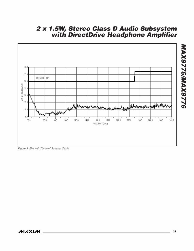
Spread-Spectrum ModulationThe MAX9775/MAX9776 feature a unique spread-spec-trum modulation that flattens the wideband spectral com-ponents. Proprietary techniques ensure that the
cycle-to-cycle variation of the switching period does notdegrade audio reproduction or efficiency (see theTypical Operating Characteristics). Select spread-spec-trum modulation mode through the I2C interface (Table2). In spread-spectrum modulation mode, the switchingfrequency varies randomly by ±30kHz around the centerfrequency (1.16MHz). The modulation scheme remainsthe same, but the period of the sawtooth waveformchanges from cycle to cycle (Figure 2). Instead of alarge amount of spectral energy present at multiples ofthe switching frequency, the energy is now spread overa bandwidth that increases with frequency. Above a fewmegahertz, the wideband spectrum looks like whitenoise for EMI purposes (see Figure 3).
2 x 1.5W, Stereo Class D Audio Subsystemwith DirectDrive Headphone Amplifier
20 ______________________________________________________________________________________
VOUT+ - VOUT-
tSW tSW tSW tSW
VIN-
VIN+
OUT+
OUT-
tON(MIN)
Figure 2. Output with an Input Signal Applied (Spread-Spectrum Modulation Mode)
MA
X9
77
5/M
AX
97
76
2 x 1.5W, Stereo Class D Audio Subsystemwith DirectDrive Headphone Amplifier
______________________________________________________________________________________ 21
FREQUENCY (MHz)
AMPL
ITUD
E (d
BμV/
m)
40.0
30.0 60.0 80.0 100.0 120.0 140.0 160.0 180.0 200.0 220.0 240.0 260.0 280.0 300.0
35.0
30.0
25.0
20.0
15.0
10.0
5.0
EN55022B LIMIT
Figure 3. EMI with 76mm of Speaker Cable
MA
X9
77
5/M
AX
97
76
2 x 1.5W, Stereo Class D Audio Subsystemwith DirectDrive Headphone Amplifier
22 ______________________________________________________________________________________
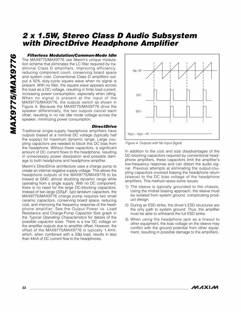
Filterless Modulation/Common-Mode IdleThe MAX9775/MAX9776 use Maxim’s unique modula-tion scheme that eliminates the LC filter required by tra-ditional Class D amplifiers, improving efficiency,reducing component count, conserving board spaceand system cost. Conventional Class D amplifiers out-put a 50% duty-cycle square wave when no signal ispresent. With no filter, the square wave appears acrossthe load as a DC voltage, resulting in finite load current,increasing power consumption, especially when idling.When no signal is present at the input of theMAX9775/MAX9776, the outputs switch as shown inFigure 4. Because the MAX9775/MAX9776 drive thespeaker differentially, the two outputs cancel eachother, resulting in no net idle mode voltage across thespeaker, minimizing power consumption.
DirectDriveTraditional single-supply headphone amplifiers haveoutputs biased at a nominal DC voltage (typically halfthe supply) for maximum dynamic range. Large cou-pling capacitors are needed to block this DC bias fromthe headphone. Without these capacitors, a significantamount of DC current flows to the headphone, resultingin unnecessary power dissipation and possible dam-age to both headphone and headphone amplifier.
Maxim’s DirectDrive architecture uses a charge pump tocreate an internal negative supply voltage. This allows theheadphone outputs of the MAX9775/MAX9776 to bebiased at GND, almost doubling dynamic range whileoperating from a single supply. With no DC component,there is no need for the large DC-blocking capacitors.Instead of two large (220µF, typ) tantalum capacitors, theMAX9775/MAX9776 charge pump requires two smallceramic capacitors, conserving board space, reducingcost, and improving the frequency response of the head-phone amplifier. See the Output Power vs. LoadResistance and Charge-Pump Capacitor Size graph inthe Typical Operating Characteristics for details of thepossible capacitor sizes. There is a low DC voltage onthe amplifier outputs due to amplifier offset. However, theoffset of the MAX9775/MAX9776 is typically 1.4mV,which, when combined with a 32Ω load, results in lessthan 44nA of DC current flow to the headphones.
In addition to the cost and size disadvantages of theDC-blocking capacitors required by conventional head-phone amplifiers, these capacitors limit the amplifier’slow-frequency response and can distort the audio sig-nal. Previous attempts at eliminating the output-cou-pling capacitors involved biasing the headphone return(sleeve) to the DC bias voltage of the headphoneamplifiers. This method raises some issues:
1) The sleeve is typically grounded to the chassis.Using the midrail biasing approach, the sleeve mustbe isolated from system ground, complicating prod-uct design.
2) During an ESD strike, the driver’s ESD structures arethe only path to system ground. Thus, the amplifiermust be able to withstand the full ESD strike.
3) When using the headphone jack as a lineout toother equipment, the bias voltage on the sleeve mayconflict with the ground potential from other equip-ment, resulting in possible damage to the amplifiers.
VIN = 0V
OUT-
OUT+
VOUT+ - VOUT- = 0V
Figure 4. Outputs with No Input Signal

Charge PumpThe MAX9775/MAX9776 feature a low-noise chargepump. The switching frequency of the charge pump ishalf the switching frequency of the Class D amplifier,regardless of the operating mode. The nominal switch-ing frequency is well beyond the audio range, and thusdoes not interfere with the audio signals, resulting in anSNR of 93dB. Although not typically required, addition-al high-frequency noise attenuation can be achieved byincreasing the size of C2 (see the Typical ApplicationCircuits). The charge pump is active in both speakerand headphone modes.
3D EnhancementThe MAX9775 features a 3D stereo enhancement func-tion, allowing the MAX9775 to widen the stereo sound fieldand immerse the listener in a cleaner, richer sound experi-ence. Note the MAX9776, mono Class D speaker amplifierdoes not feature 3D stereo enhancement.
As stereo speaker applications become more compact,the quality of stereophonic sound is jeopardized.
With Maxim’s 3D stereo enhancement, it is possible toemulate stereo sound in situations where the speakersmust be positioned close together. As shown in Figure6, wave interference can be used to cancel the leftchannel in the vicinity of the listener’s right ear and viceversa. This technique can yield an apparent separationbetween the speakers that is a factor of four or greaterthan the actual physical separation.
The external capacitors CL_L, CL_H, CR_L, and CR_Hset the starting and stopping range of the 3D effect.CL_H and CR_H are for the lower limit (in the MAX9775Typical Application Circuit, it is 1kHz), CR_L and CL_Lare for the higher limit (10kHz). The internal resistor istypically 7kΩ and the frequencies are calculated as:
where R = 7kΩ and C = CR_H and CL_H.
where R = 7kΩ and C = CR_L and CL_L.
For example, with CR_L = CL_L = 2.2nF and CR_H =CL_H = 22nF, the 3D start frequency is 1kHz and the3D stop frequency is 10kHz.
Enabling the 3D sound effect results in an apparent 6dBgain because the internal left and right signals are mixedtogether. This gain can be nulled by volume adjustingthe left and right signals. The volume control can be pro-grammed through the I2C-compatible interface to com-pensate for the extra 6dB increase in gain. For example,
31
2D STOP
RC_ =
π
31
2D START
RC_ =
π
MA
X9
77
5/M
AX
97
76
2 x 1.5W, Stereo Class D Audio Subsystemwith DirectDrive Headphone Amplifier
______________________________________________________________________________________ 23
VDD / 2
VDD
GND
+VDD
-VDD
GNDVOUT
VOUT
CONVENTIONAL DRIVER-BIASING SCHEME
DirectDrive BIASING SCHEME
Figure 5. Traditional Amplifier Output vs. MAX9775/MAX9776DirectDrive Output
+
+
d
QR
IL
IR
QL
RIGHT
LEFT
RIGHT
LEFT
LISTENER
Figure 6. MAX9775 3D Stereo Enhancement

MA
X9
77
5/M
AX
97
76 if the right and left volume controls are set for a maxi-
mum gain 0dB (11111 in Table 7, IN+6dB = 0 from Table10) before the 3D effect is activated, the volume controlshould be programmed to -6dB (11001 in Table 7)immediately after the 3D effect has been activated.
Signal PathThe audio inputs of the MAX9775/MAX9776—INA, INB,and INC—are preamplified and then mixed by the inputmixer to create three internal signals: Left (L), Right (R),and Mono (M). Tables 5a and 5b show how the inputsare mixed to create L, R, and M. These signals are thenindependently volume adjusted by the L, R, and M vol-ume control and routed to the output mixer. The outputmixer mixes the internal L, R, and M signals to create avariety of audio mixes that are output to the headphonespeaker and mono receiver amplifiers. Figure 6 showsthe signal path that the audio signals take.
Signal amplification takes place in three stages. In thefirst stage, the inputs (INA, INB, and INC) are pre-amplified. The amount by which each input is amplifiedis determined by the bits INA+20dB (B4 in the InputMode Control Register) and IN+6dB (B3 in the GlobalControl Register). After preamplification, they are mixed
in the Input Mixer to create the internal signals L, R,and M.
In the second stage of amplification, the internal L, R,and M signals are independently volume adjusted.
Finally, each output amplifier has its own internal gain.The speaker, headphone, and mono receiver amplifiershave fixed gains of 12dB, 3dB, and 3dB, respectively.
Current-Limit and Thermal ProtectionThe MAX9775/MAX9776 feature current limiting andthermal protection to protect the device from short cir-cuits and overcurrent conditions. The headphoneamplifier pulses in the event of an overcurrent conditionwith a pulse every 100µs as long as the condition ispresent. Should the current still be high, the abovecycle is repeated. The speaker amplifier current-limitprotection clamps the output current without shuttingdown the output. This can result in a distorted output.Current is limited to 1.6A in the speaker amplifiers and170mA in the headphone and mono receiver amplifiers.
The MAX9775/MAX9776 have thermal protection thatdisables the device at +150°C until the temperaturedecreases to +120°C.
2 x 1.5W, Stereo Class D Audio Subsystemwith DirectDrive Headphone Amplifier
24 ______________________________________________________________________________________
INPUTMIXERINPUT
PREAMPLIFIER
INPUT A:0dB, 6dB, 20dB
-75dB TO 0dB
-75dB TO 0dB0dB TO 6dB
MVOLMONO+6dB
LVOL
-75dB TO 0dB
RVOL
INPUT B AND C:0dB, 6dB
OUTPUTMIXER
3dB
3dB
12dB
SPEAKER
HEADPHONE
RECEIVERMONO
Figure 7. Signal Path
Click-and-Pop SuppressionIn conventional single-supply headphone amplifiers, theoutput-coupling capacitor is a major contributor of audi-ble clicks and pops. Upon startup, the amplifier chargesthe coupling capacitor to its bias voltage, typically half thesupply. Likewise, during shutdown, the capacitor is dis-charged to GND. This results in a DC shift across thecapacitor, which, in turn, appears as an audible transientat the speaker. Since the MAX9775/MAX9776 headphoneamplifier does not require output-coupling capacitors, thisproblem does not arise.
In most applications, the output of the preamplifier dri-ving the MAX9775/MAX9776 has a DC bias of typicallyhalf the supply. During startup, the input-couplingcapacitor is charged to the preamplifier’s DC bias volt-age, resulting in a DC shift across the capacitor and anaudible click/pop. An internal delay of 30ms eliminatesthe click/pop caused by the input filter.
ShutdownThe MAX9775/MAX9776 feature a 0.1µA hard shutdownmode that reduces power consumption to extend batterylife and a soft shutdown where current consumption istypically 8.5µA. Hard shutdown is controlled by connect-ing the SHDN pin to GND, disabling the amplifiers, biascircuitry, charge pump, and I2C. In shutdown, the head-phone amplifier output impedance is 1.4kΩ and thespeaker output impedance is 300kΩ. Similarly, theMAX9775/MAX9776 enter soft-shutdown when the SHDNbit = 0 (see Table 2). The I2C interface is active and thecontents of the command register are not affected whenin soft-shutdown. This allows the master to write to theMAX9775/MAX9776 while in shutdown. The I2C interfaceis completely disabled in hardware shutdown. When theMAX9775/MAX9776 are re-enabled the default settingsare applied (see Table 3).
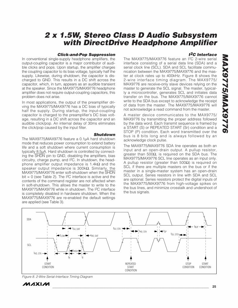
I2C InterfaceThe MAX9775/MAX9776 feature an I2C 2-wire serialinterface consisting of a serial data line (SDA) and aserial clock line (SCL). SDA and SCL facilitate commu-nication between the MAX9775/MAX9776 and the mas-ter at clock rates up to 400kHz. Figure 8 shows the2-wire interface timing diagram. The MAX9775/MAX9776 are receive-only slave devices relying on themaster to generate the SCL signal. The master, typical-ly a microcontroller, generates SCL and initiates datatransfer on the bus. The MAX9775/MAX9776 cannotwrite to the SDA bus except to acknowledge the receiptof data from the master. The MAX9775/MAX9776 willnot acknowledge a read command from the master.
A master device communicates to the MAX9775/MAX9776 by transmitting the proper address followedby the data word. Each transmit sequence is framed bya START (S) or REPEATED START (Sr) condition and aSTOP (P) condition. Each word transmitted over thebus is 8 bits long and is always followed by anacknowledge clock pulse.
The MAX9775/MAX9776 SDA line operates as both aninput and an open-drain output. A pullup resistor,greater than 500Ω, is required on the SDA bus. TheMAX9775/MAX9776 SCL line operates as an input only.A pullup resistor (greater than 500Ω) is required onSCL if there are multiple masters on the bus or if themaster in a single-master system has an open-drainSCL output. Series resistors in line with SDA and SCLare optional. Series resistors protect the digital inputs ofthe MAX9775/MAX9776 from high-voltage spikes onthe bus lines, and minimize crosstalk and undershoot ofthe bus signals.
MA
X9
77
5/M
AX
97
76
2 x 1.5W, Stereo Class D Audio Subsystemwith DirectDrive Headphone Amplifier
______________________________________________________________________________________ 25
SCL
SDA
STARTCONDITION
STOPCONDITION
REPEATED START
CONDITION
START CONDITION
tHD, STA
tSU, STAtHD, STA tSP
tBUF
tSU, STOtLOW
tSU, DAT
tHD, DAT
tHIGH
tR tF
Figure 8. 2-Wire Serial-Interface Timing Diagram

MA
X9
77
5/M
AX
97
76 Bit Transfer
One data bit is transferred during each SCL cycle. Thedata on SDA must remain stable during the high periodof the SCL pulse. Changes in SDA while SCL is highare control signals (see the START and STOPConditions section). SDA and SCL idle high when theI2C bus is not busy.
START and STOP ConditionsA master device initiates communication by issuing aSTART condition. A START condition is a high-to-lowtransition on SDA with SCL high. A STOP condition is alow-to-high transition on SDA while SCL is high (Figure9). A START (S) condition from the master signals thebeginning of a transmission to the MAX9775/MAX9776.The master terminates transmission, and frees the bus,by issuing a STOP (P) condition. The bus remains activeif a REPEATED START (Sr) condition is generatedinstead of a STOP condition.
Early STOP ConditionsThe MAX9775/MAX9776 recognize a STOP condition atany point during data transmission except if the STOPcondition occurs in the same high pulse as a STARTcondition.
Slave AddressThe MAX9775/MAX9776 are available with one presetslave address (see Table 1). The address is defined as
the seven most significant bits (MSBs) followed by theRead/Write bit. The address is the first byte of informa-tion sent to the MAX9775/MAX9776 after the STARTcondition. The MAX9775/MAX9776 are slave devicesonly capable of being written to. The Read/Write bitshould be a zero when configuring the MAX9775/MAX9776.
AcknowledgeThe acknowledge bit (ACK) is a clocked 9th bit that theMAX9775/MAX9776 use to handshake receipt of eachbyte of data (see Figure 10). The MAX9775/MAX9776pull down SDA during the master-generated 9th clockpulse. Monitoring ACK allows for detection of unsuc-cessful data transfers. An unsuccessful data transferoccurs if a receiving device is busy or if a system faulthas occurred. In the event of an unsuccessful datatransfer, the bus master may reattempt communications.
2 x 1.5W, Stereo Class D Audio Subsystemwith DirectDrive Headphone Amplifier
26 ______________________________________________________________________________________
SCL
SDA
S Sr P
Figure 9. START, STOP, and REPEATED START Conditions
1SCL
STARTCONDITION
SDA
2 8 9
CLOCK PULSE FORACKNOWLEDGMENT
ACKNOWLEDGE
NOT ACKNOWLEDGE
SLAVE ADDRESSPART
A6 A5 A4 A3 A2 A1 A0 R/W
MAX9775 1 0 0 1 1 0 0 0
MAX9776 1 0 0 1 1 0 1 0
Figure 10. Acknowledge
Table 1. MAX9775/MAX9776 Address Map

Write Data FormatA write to the MAX9775/MAX9776 includes transmis-sion of a START condition, the slave address with theR/W bit set to 0 (Table 1), one byte of data to configurethe Command Register, and a STOP condition. Figure11 illustrates the proper format for one frame.
The MAX9775/MAX9776 only accept write data, butthey acknowledge the receipt of the address byte withthe R/W bit set high. The MAX9775/MAX9776 do notwrite to the SDA bus in the event that the R/W bit is sethigh. Subsequently, the master reads all 1’s from theMAX9775/MAX9776. Always set the R/W bit to zero toavoid this situation.
Programming the MAX9775/MAX9776The MAX9775/MAX9776 are programmed through 6control registers. Each register is addressed by the 3MSBs (B5–B7) followed by 5 configure bits (B0–B4) asshown in Table 2. Correct programming of theMAX9775/MAX9776 requires writing to all 6 control reg-isters. Upon power-on, their default settings are as list-ed in Table 3.
MA
X9
77
5/M
AX
97
76
2 x 1.5W, Stereo Class D Audio Subsystemwith DirectDrive Headphone Amplifier
______________________________________________________________________________________ 27
S ACK0
ACKNOWLEDGE FROM MAX9775/MAX9776
R/W ACKNOWLEDGEFROM MAX9775/MAX9776
B7 B6 B5 B4 B3 B2COMMAND BYTE IS STORED ON
RECEIPT OF STOP CONDITION
ACK P
B1 B0
SLAVE ADDRESS COMMAND BYTE
Figure 11. Write Data Format Example
B7 B6 B5 B4 B3 B2 B1 B0FUNCTION
COMMAND DATA
Input Mode Control 0 0 0 INA+20dB INMODE (Tables 5a and 5b)
Mono Volume Control 0 0 1 MVOL (Table 7)
Left Volume Control 0 1 0 LVOL (Table 7)
Right Volume Control 0 1 1 RVOL (Table 7)
Output Mode Control 1 0 0 MONO+6dB OUTMODE (Table 9)
Global Control Register 1 0 1 SHDN IN+6dB MUTE SSM 3D/MONO
Table 2. Control Registers
COMMAND DATA DESCRIPTION
Input Mode (000) 10000 Input A gain = +20dB; input A, B, and C singled-ended stereo inputs
Mono Volume (001) 11111 Maximum volume
Left Volume (010) 11111 Maximum volume
Right Volume (011) 11111 Maximum volume
Output Mode (100) 01000 0dB of extra mono gain, mode 8: stereo headphone, stereo speaker
Global Control Register (101) 00011 Powered-off, input B/C gain = 0dB, MUTE off, SSM on, 3D/MONO on
Table 3. Power-On Reset Conditions

MA
X9
77
5/M
AX
97
76
The MAX9775/MAX9776 have three flexible inputs thatcan be configured as single-ended stereo inputs or dif-ferential mono inputs. All input signals are summed intothree unique signals—Left (L), Right (R), and Mono(M)—which are routed to the output amplifiers. The bitINA+20dB allows the option of boosting low-level sig-nals on INA. INA+20dB can be set as follows:
1 = Input A’s gain +20dB for low-level signals such asFM receivers.
0 = Input A’s gain is either 0dB or +6dB as set byIN+6dB (bit B3 of the Control Register).
Tables 5a and 5b show how the inputs—INA, INB, andINC—are mixed to create the internal signals Left (L),Right (R), and Mono (M).
2 x 1.5W, Stereo Class D Audio Subsystemwith DirectDrive Headphone Amplifier
28 ______________________________________________________________________________________
Input Mode Control
REGISTER B7 B6 B5 B4 B3 B2 B1 B0
Input Mode Control 0 0 0 INA+20dB INMODE (Tables 5a and 5b )
Table 4. Input Mode Control Register
PROGRAMMING MODE INPUT CONFIGURATIONINMODE
B3 B2 B1 B0INA1 INA2 INB1 INB2 INC1 INC2
0 0 0 0 L R L R L R0 0 0 1 L R L R M+ M-0 0 1 0 L R M+ M- L R0 0 1 1 L R M+ M- M+ M-0 1 0 0 L R R+ R- L+ L-0 1 0 1 L R L+ L- R+ R-0 1 1 0 M+ M- L R L R0 1 1 1 M+ M- L R M+ M-1 0 0 0 M+ M- M+ M- L R1 0 0 1 M+ M- M+ M- M+ M-1 0 1 0 M+ M- R+ R- L+ L-1 0 1 1 M+ M- L+ L- R+ R-
Table 5a. Input Mode
PROGRAMMING MODE INTERNAL SIGNALS LEFT (L), RIGHT (R), AND MONO (M)INMODE
B3 B2 B1 B0L R M
0 0 0 0 INA1 + INB1 + INC1 INA2 + INB2 + INC2 —0 0 0 1 INA1 + INB1 INA2 + INB2 INC1 - INC20 0 1 0 INA1 + INC1 INA2 + INC2 INB1 - INB20 0 1 1 INA1 INA2 (INB1 - INB2) + (INC1 - INC2)0 1 0 0 INA1 + (INC1 - INC2) INA2 + (INB1 - INB2) —0 1 0 1 INA1 + (INB1 - INB2) INA2 + (INC1 - INC2) —0 1 1 0 INB1 + INC1 INB2 + INC2 INA1 - INA20 1 1 1 INB1 INB2 (INA1 - INA2) + (INC1 - INC2)1 0 0 0 INC1 INC2 (INA1 - INA2) + (INB1 - INB2)
1 0 0 1 — —(INA1 - INA2) + (INB1 - INB2)
+ (INC1 - INC2)
1 0 1 0 INC1 - INC2 INB1 - INB2 INA1 - INA21 0 1 1 INB1 - INB2 INC1 - INC2 INA1 - INA2
Table 5b. Internal Signals L, R, and M

The MAX9775/MAX9776 have separate volume controlsfor each of the internal signals: Left (L), Right (R), andMono (M). The final gain of each signal is determinedby the way the following bits are set: MVOL, LVOL,
RVOL, INA+20dB, IN+6dB, and MONO+6dB. Table 7shows how to configure the L, R, and M amplifiers forspecific gains.
MA
X9
77
5/M
AX
97
76
2 x 1.5W, Stereo Class D Audio Subsystemwith DirectDrive Headphone Amplifier
______________________________________________________________________________________ 29
Mono/Left/Right Volume Control
REGISTER B7 B6 B5 B4 B3 B2 B1 B0
Mono Volume Control 0 0 1 MVOL
Left Volume Control 0 1 0 LVOL
Right Volume Control 0 1 1 RVOL
Table 6. Mono/Left/Right Volume Control Registers
MVOL/LVOL/RVOL
B4 B3 B2 B1 B0GAIN (dB)
0 0 0 0 0 Mute
0 0 0 0 1 -75
0 0 0 1 0 -71
0 0 0 1 1 -67
0 0 1 0 0 -63
0 0 1 0 1 -59
0 0 1 1 0 -55
0 0 1 1 1 -51
0 1 0 0 0 -47
0 1 0 0 1 -44
0 1 0 1 0 -41
0 1 0 1 1 -38
0 1 1 0 0 -35
0 1 1 0 1 -32
0 1 1 1 0 -29
0 1 1 1 1 -26
MVOL/LVOL/RVOL
B4 B3 B2 B1 B0GAIN (dB)
1 0 0 0 0 -23
1 0 0 0 1 -21
1 0 0 1 0 -19
1 0 0 1 1 -17
1 0 1 0 0 -15
1 0 1 0 1 -13
1 0 1 1 0 -11
1 0 1 1 1 -9
1 1 0 0 0 -7
1 1 0 0 1 -6
1 1 0 1 0 -5
1 1 0 1 1 -4
1 1 1 0 0 -3
1 1 1 0 1 -2
1 1 1 1 0 -1
1 1 1 1 1 0
Table 7. Volume Control Settings

MA
X9
77
5/M
AX
97
76
MONO+6dB in the Output Mode Control register allowsan extra 6dB of gain on the internal mono signal:
1 = Additional 6dB of gain is applied to the internalMono (M) signal path.
0 = No additional gain is applied to the Internal Mono(M) signal path.
The MAX9775 has five output amplifiers: a monoreceiver amplifier, a stereo DirectDrive headphone
amplifier, and a stereo Class D amplifier. The MAX9776has four output amplifiers: a mono receiver amplifier, astereo DirectDrive headphone amplifier, and a monoClass D amplifier.
Table 9 shows how each of the three internal signals—Left (L), Right (R), and Mono (M)—are mixed and rout-ed to the various outputs.
2 x 1.5W, Stereo Class D Audio Subsystemwith DirectDrive Headphone Amplifier
30 ______________________________________________________________________________________
Output Mode Control
REGISTER B7 B6 B5 B4 B3 B2 B1 B0
Output Mode Control 1 0 0 MONO+6dB OUTMODE (Table 9)
Table 8. Output Mode Control Register
OUTMODE MAX9775 MAX9776MODE
B3 B2 B1 B0RECEIVER LEFT HP RIGHT HP
LEFT SPK RIGHT SPK
0 0 0 0 0 — — — — — —
1 0 0 0 1 M — — — — —
2 0 0 1 0 — — — M M M
3 0 0 1 1 — M M M M M
4 0 1 0 0 — M M — — —
5 0 1 0 1 — — — — — —
6 0 1 1 0 1/2 (L + R) — — — — —
7 0 1 1 1 — — — L R L + R
8 1 0 0 0 — L R L R L + R
9 1 0 0 1 — L R — — —
10 1 0 1 0 — — — — — —
11 1 0 1 1 M + 1/2 (L + R) — — — — —
12 1 1 0 0 — — — L + M R + M L + R + 2M
13 1 1 0 1 — L + M R + M L + M R + M L + R + 2M
14 1 1 1 0 — L + M R + M — — —
15 1 1 1 1 MUTE MUTE MUTE MUTE MUTE MUTE
Table 9. Output Modes
— = Amplifier off.L = Left signal.R = Right signal.M = Mono signal.

The Global Control Register is used for global configu-rations, those affecting all inputs and outputs. The bits
in the control register are shown in Table 11.
MA
X9
77
5/M
AX
97
76
2 x 1.5W, Stereo Class D Audio Subsystemwith DirectDrive Headphone Amplifier
______________________________________________________________________________________ 31
Global Control Register
REGISTER B7 B6 B5 B4 B3 B2 B1 B0
Global Control Register 1 0 1 SHDN IN+6dB MUTE SSM 3D/MONO
Table 10. Global Control Register
BIT NAME FUNCTION
B4 SHDN1 = Normal operation0 = Low-power shutdown mode. I2C settings are saved.
B3 IN+6dB
1 = All input signals are boosted by 6dB.0 = All input signals are passed un-amplified.This bit does not affect INA if the INA+20dB bit (B4 of the Input Mode Control Register) is set to1, in which case INA is boosted by 20dB.
B2 MUTE1 = Mute all outputs.0 = All outputs are active.
B1 SSM1 = Spread-spectrum Class D modulation.0 = Fixed-frequency Class D modulation.
B0 3D/MONO
MAX9775:1 = 3D Enhancement is on.0 = 3D Enhancement is off.1 = Speakers will output L+R in modes 7, 8, 12, and 13 (see Table 9).0 = Speakers will output L in modes 7, 8, 12, and 13 (see Table 9).
Table 11. Global Control Register Configurations
Applications InformationClass D Filterless Operation
Traditional Class D amplifiers require an output filter torecover the audio signal from the amplifier’s PWM out-put. The filters add cost, increase the solution size ofthe amplifier, and can decrease efficiency. The tradi-tional PWM scheme uses large differential outputswings (2 x VDD(P-P)) and causes large ripple currents.Any parasitic resistance in the filter components resultsin a loss of power, lowering the efficiency.
The MAX9775/MAX9776 do not require an output filter.The device relies on the inherent inductance of thespeaker coil and the natural filtering of both the speak-er and the human ear to recover the audio componentof the square-wave output. Eliminating the output filterresults in a smaller, less costly, more efficient solution.
Because the switching frequency of the MAX9775/MAX9776 speaker output is well beyond the bandwidth
of most speakers, voice coil movement due to thesquare-wave frequency is very small. Although this move-ment is small, a speaker not designed to handle the addi-tional power may be damaged. For optimum results use aspeaker with a series inductance > 10µH. Typical 8Ωspeakers, for portable audio applications, exhibit seriesinductances in the 20µH to 100µH range.
Input AmplifierDifferential Input
The MAX9775/MAX9776 feature a programmable differ-ential input structure, making it compatible with manyCODECs, and offering improved noise immunity over asingle-ended input amplifier. In devices such as cellphones, high-frequency signals from the RF transmittercan be picked up by the amplifier’s input traces. Thesignals appear at the amplifier’s inputs as common-mode noise. A differential input amplifier amplifies thedifference of the two inputs and any signal common toboth is cancelled.

Single-Ended InputThe MAX9775/MAX9776 can be configured as a single-ended input amplifier by appropriately configuring theInput Control Register (see Tables 5a and 5b).
DC-Coupled InputThe input amplifier can accept DC-coupled inputs thatare biased to the amplifier’s bias voltage. DC-couplingeliminates the input-coupling capacitors; reducing com-ponent count to potentially six external components(see the Typical Application Circuits). However, thehighpass filtering effect of the capacitors is lost, allow-ing low-frequency signals to feed through to the load.
Unused InputsConnect any unused input pin directly to VBIAS. Thissaves input capacitors on unused inputs and providesthe highest noise immunity on the input.
Component SelectionInput Filter
An input capacitor (CIN) in conjunction with the inputimpedance of the MAX9775/MAX9776 form a highpassfilter that removes the DC bias from the incoming signal.The AC-coupling capacitor allows the amplifiers to auto-matically bias the signal to an optimum DC level.Assuming zero source impedance, the -3dB point of thehighpass filter is given by:
Choose CIN so that f-3dB is well below the lowest fre-quency of interest. Use capacitors whose dielectricshave low-voltage coefficients, such as tantalum or alu-minum electrolytic. Capacitors with high-voltage coeffi-cients, such as ceramics, may result in increaseddistortion at low frequencies.
Other considerations when designing the input filterinclude the constraints of the overall system and theactual frequency band of interest. Although high-fidelityaudio calls for a flat-gain response between 20Hz and20kHz, portable voice-reproduction devices such as cellphones and two-way radios need only concentrate onthe frequency range of the spoken human voice (typi-
cally 300Hz to 3.5kHz). In addition, speakers used inportable devices typically have a poor response below300Hz. Taking these two factors into consideration, theinput filter may not need to be designed for a 20Hz to20kHz response, saving both board space and costdue to the use of smaller capacitors.
Class D Output FilterThe MAX9775/MAX9776 do not require a Class D out-put filter. The devices pass EN55022B emission stan-dards with 152mm of unshielded speaker cables.However, output filtering can be used if a design is fail-ing radiated emissions due to board layout or cablelength, or the circuit is near EMI-sensitive devices. Usea ferrite bead filter when radiated frequencies above10MHz are of concern. Use an LC filter when radiatedfrequencies below 10MHz are of concern, or when longleads (> 152mm) connect the amplifier to the speaker.Figure 12 shows optional speaker amplifier output filters.
External Component SelectionBIAS Capacitor
VBIAS is the output of the internally generated DC biasvoltage. The VBIAS bypass capacitor, CVBIAS improvesPSRR and THD+N by reducing power supply and othernoise sources at the common-mode bias node, andalso generates the clickless/popless, startup/shutdownDC bias waveforms for the speaker amplifiers. BypassVBIAS with a 1µF capacitor to GND.
fR CdB
IN IN− =3
12π
MA
X9
77
5/M
AX
97
76
2 x 1.5W, Stereo Class D Audio Subsystemwith DirectDrive Headphone Amplifier
32 ______________________________________________________________________________________
OUT_+
OUT_-
33μH
33μH
0.47μF
0.033μF0.1μF
22Ω
22Ω0.033μF0.1μF
Figure 12. Speaker Amplifier Output Filter
MA
X9
77
5/M
AX
97
76
2 x 1.5W, Stereo Class D Audio Subsystemwith DirectDrive Headphone Amplifier
______________________________________________________________________________________ 33
Table 12. Suggested Capacitor ManufacturersSUPPLIER PHONE FAX WEBSITE
Taiyo Yuden 800-348-2496 847-925-0899 www.t-yuden.com
TDK 807-803-6100 847-390-4405 www.component.tdk.com
Charge-Pump Capacitor SelectionUse capacitors with an ESR less than 100mΩ for opti-mum performance. Low-ESR ceramic capacitors mini-mize the output resistance of the charge pump. Mostsurface-mount ceramic capacitors satisfy the ESRrequirement. For best performance over the extendedtemperature range, select capacitors with an X7R dielec-tric or better. Table 12 lists suggested manufacturers.
Flying Capacitor (C1)The value of the flying capacitor (C1) affects the outputresistance of the charge pump. A C1 value that is toosmall degrades the device’s ability to provide sufficientcurrent drive, which leads to a loss of output voltage.Increasing the value of C1 reduces the charge-pump out-put resistance to an extent. Above 1µF, the on-resistanceof the switches and the ESR of C1 and C2 dominate.
Output Capacitor (C2)The output capacitor value and ESR directly affect theripple at CPVSS. Increasing the value of C2 reducesoutput ripple. Likewise, decreasing the ESR of C2reduces both ripple and output resistance. Lowercapacitance values can be used in systems with lowmaximum output power levels. See the Output Powervs. Load Resistance and Charge-Pump Capacitor Sizegraph in the Typical Operating Characteristics.
CPVDD Bypass Capacitor (C3)The CPVDD bypass capacitor (C3) lowers the outputimpedance of the power supply and reduces theimpact of the MAX9775/MAX9776’s charge-pumpswitching transients. Bypass CPVDD with C3 to PGNDand place it physically close to the CPVDD and PGND.Use a value for C3 that is equal to C1.
Supply Bypassing, Layout, and GroundingProper layout and grounding are essential for optimumperformance. Use large traces for the power-supplyinputs and amplifier outputs to minimize losses due toparasitic trace resistance. Large traces also aid in mov-ing heat away from the package. Proper groundingimproves audio performance, minimizes crosstalkbetween channels, and prevents any switching noisefrom coupling into the audio signal. Connect PGND andGND together at a single point on the PCB. Route alltraces that carry switching transients away from GNDand the traces/components in the audio signal path.
Connect all of the power-supply inputs (CPVDD, VDD,and PVDD) together. Bypass CPVDD with a 1µF capaci-tor to CPGND. Bypass VDD with 1µF capacitor to GND.Bypass PVDD with a 1µF capacitor in parallel with a0.1µF capacitor to PGND. Place the bypass capacitorsas close to the MAX9775/MAX9776 as possible. Placea bulk capacitor between PVDD and PGND if needed.
Use large, low-resistance output traces. Current drawnfrom the outputs increases as load impedancedecreases. High output trace resistance decreases thepower delivered to the load. Large output, supply, andGND traces also allow more heat to move from theMAX9775/MAX9776 to the PCB, decreasing the thermalimpedance of the circuit.
TQFN Applications InformationThe MAX9776 TQFN-EP package features an exposedthermal pad on its underside. This pad lowers thepackage’s thermal impedance by providing a directheat conduction path from the die to the PCB. Theexposed pad is internally connected to GND. Connectthe exposed thermal pad to the PCB GND plane.
WLP Applications InformationFor the latest application details on WLP construction,dimensions, tape carrier information, PCB techniques,bump-pad layout, and recommended reflow tempera-ture profile, as well as the latest information of reliabilitytesting results, refer to Application Note 1891:Understanding the Basics of the Wafer-Level Chip-Scale Package (WL-CSP) available on Maxim’s websiteat www.maxim-ic.com/ucsp.
WLP Thermal ConsiderationWhen operating at maximum output power, the WLPthermal dissipation can become a limiting factor. TheWLP package does not dissipate as much power as aTQFN and as a result will operate at a higher tempera-ture. At peak output power into a 4Ω load, theMAX9775/MAX9776 can exceed its thermal limit, trig-gering thermal protection. As a result, do not choosethe WLP package when maximum output power into 4Ωis required.

MA
X9
77
5/M
AX
97
76
2 x 1.5W, Stereo Class D Audio Subsystemwith DirectDrive Headphone Amplifier
34 ______________________________________________________________________________________
Chip InformationPROCESS: BiCMOS
Pin Configurations
TOP VIEW
TQFN-EP*
32 28293031 252627
I.C.
INA1
PGND
I.C.
SHDN
INA2
I.C.
GND
10 13 1514
*EP
1611 129
CPV D
D
VBIA
S
C1P
C1N
CPGN
D
CPV S
S
INC1 HP
L
17
18
19
20
21
22
23 I.C.
24 INB1
INB2
VDD
OUTRx
INC2
HPR
VSS
2
3
4
5
6
7
8I.C.
I.C.
SDA
OUT+
PGND
SCL
OUT-
1PVDD
MAX9776
+
TOP VIEW(BUMPS ON BOTTOM)
MAX9775
C1P CPGND C1NCPVDD
1
A
B
C
D
2 3 4
OUTL+ SDA
PGND SCL
WLP
E
F
PVDD OUTR- PGND OUTR+
CPVSS HPL
CL_H VBIAS INC1CL_L VSS HPR
5 6
INC2 OUTRx
INB2 VDD
CR_H GND
OUTL- SHDN INA1 INA2 INB1 CR_L
MAX9776
C1P CPGND C1NCPVDD
1
A
B
C
D
2 3 4
OUT+ SDA
PGND SCL
WLP
E
F
PVDD I.C. PGND I.C.
CPVSS HPL
I.C. VBIAS INC1I.C. VSS HPR
5 6
INC2 OUTRx
INB2 VDD
I.C. GND
OUT- SHDN INA1 INA2 INB1 I.C.
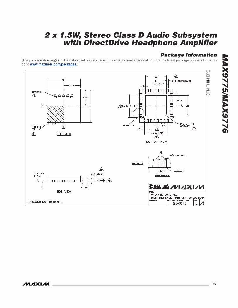
MA
X9
77
5/M
AX
97
76
Package Information(The package drawing(s) in this data sheet may not reflect the most current specifications. For the latest package outline informationgo to www.maxim-ic.com/packages.)
QFN
TH
IN.E
PS
2 x 1.5W, Stereo Class D Audio Subsystemwith DirectDrive Headphone Amplifier
______________________________________________________________________________________ 35

MA
X9
77
5/M
AX
97
76
2 x 1.5W, Stereo Class D Audio Subsystemwith DirectDrive Headphone Amplifier
36 ______________________________________________________________________________________
Package Information (continued)(The package drawing(s) in this data sheet may not reflect the most current specifications. For the latest package outline informationgo to www.maxim-ic.com/packages.)

MA
X9
77
5/M
AX
97
76
2 x 1.5W, Stereo Class D Audio Subsystemwith DirectDrive Headphone Amplifier
______________________________________________________________________________________ 37
WLP
PK
G.E
PS
Package Information (continued)(The package drawing(s) in this data sheet may not reflect the most current specifications. For the latest package outline informationgo to www.maxim-ic.com/packages.)
PACKAGE TYPE PACKAGE CODE DOCUMENT NO.
36 WLP W363A3+3 21-0024
32 TQFN-EP T3255-4 21-0140
MA
X9
77
5/M
AX
97
76
2 x 1.5W, Stereo Class D Audio Subsystemwith DirectDrive Headphone Amplifier
Maxim cannot assume responsibility for use of any circuitry other than circuitry entirely embodied in a Maxim product. No circuit patent licenses areimplied. Maxim reserves the right to change the circuitry and specifications without notice at any time.
38 ____________________Maxim Integrated Products, 120 San Gabriel Drive, Sunnyvale, CA 94086 408-737-7600
© 2008 Maxim Integrated Products is a registered trademark of Maxim Integrated Products, Inc.
Revision History
REVISIONNUMBER
REVISIONDATE
DESCRIPTIONPAGES
CHANGED
0 3/07 Initial release —
1 7/07 Initial release of MAX9776 UCSP package and updated Tables 3 and 5b 1, 7, 27, 28
2 9/07Initial release of MAX9775 UCSP and removal of MAX9775 TQFN, updated PinDescription and Table 9
1, 12, 15, 30, 33, 34
3 1/08 Updated the Typical Application Circuits 17, 18
4 8/08 Changed package code and drawing 1, 33, 34, 37