2 Review of Scanning Probe Microscopy Techniques
33
2 Review of Scanning Probe Microscopy Techniques Νόμῳ γάρ φησι γλυκὺ [καὶ] νόμῳ πικρόν, νόμῳ ψυχρόν, νόμῳ χροιή, ἐτεῇ δὲ ἄτομα καὶ κενόν. (Democritus, fragment9) 2.1 Introduction 2.1.1 Motivation T he atomic force microscope (afm) playsanimportantpartintheresearchcovered in this thesis. I investigate local anodic oxidation (lao)—a technology based on the afm—as one approach for fabricating the antidot patterns studied in Chapter 7. Its adap- tion to the materials and the patterns at the focus of this work is expounded in Chapter 3. Chapters4and5alsouse afm micrographsforevaluationpurposes. Toapprehendthechal- lengesof afm-basedlithographyandcorrectlyinterpret afm imagesathoroughunderstand- ing of the capabilities and limitations of the instrument is indispensable. Collecting the background information in this chapter allows me to concentrate on the subjectmatterlateron.ereaderwillhopefullyfinditaconvenientplacetolookupdetailed information; those who are intimately familiar with the theory and application of scanning probe microscopes (spms) are free to skip it on first reading. Although I have stressed the common features of all spmswhereverpossible,thefocusisbynecessityonthe afm.Ihave alsotakentheopportunitytoroundofftheaccountbybrieflycoveringtopicssuchasthenear 10
Transcript of 2 Review of Scanning Probe Microscopy Techniques
2 Review of Scanning Probe Microscopy Techniques
Νόµῳ γάρ φησι γλυκὺ [καὶ] νόµῳ πικρόν,νόµῳ ψυχρόν, νόµῳ χροιή, ἐτεῇ δὲ ἄτοµα καὶκενόν.
(Democritus, fragment 9)
2.1 Introduction
2.1.1 Motivation
The atomic force microscope (afm) plays an important part in the research covered
in this thesis. I investigate local anodic oxidation (lao)—a technology based on the
afm—as one approach for fabricating the antidot patterns studied in Chapter 7. Its adap-
tion to the materials and the patterns at the focus of this work is expounded in Chapter 3.
Chapters 4 and 5 also use afmmicrographs for evaluation purposes. To apprehend the chal-
lenges of afm-based lithography and correctly interpretafm images a thorough understand-
ing of the capabilities and limitations of the instrument is indispensable.
Collecting the background information in this chapter allows me to concentrate on the
subjectmatter later on. ¿e readerwill hopefully �nd it a convenient place to look updetailed
information; those who are intimately familiar with the theory and application of scanning
probe microscopes (spms) are free to skip it on �rst reading. Although I have stressed the
common features of all spms wherever possible, the focus is by necessity on the afm. I have
also taken the opportunity to round o� the account by brie�y covering topics such as the near
10
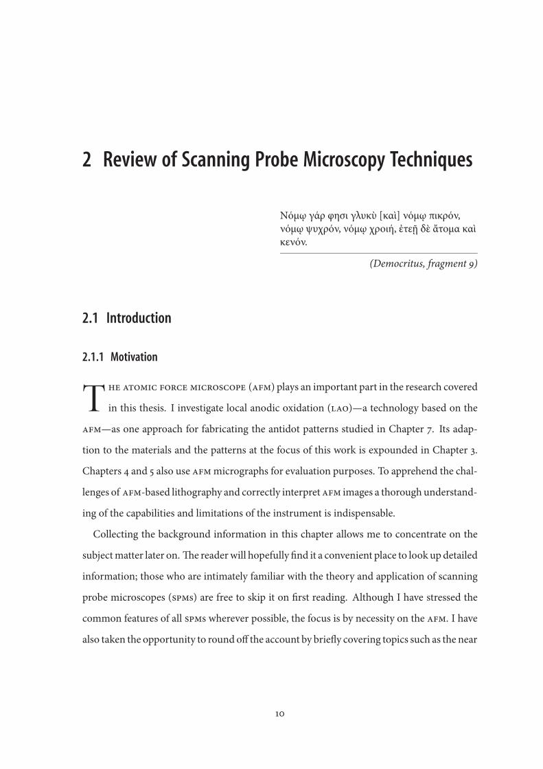
2 Review of Scanning Probe Microscopy Techniques
zpositioner
feedbackcontroller
tip–sample distance
error signal
tip–samplesystem detectors
primary measurement
secondary measurements display anddata storage
scanning signal
coarsepositioner
x , ypositioner
Figure 2.1: Schematic diagram of an spm
�eld scanning optical microscope (nfsom, Sec. 2.2.3) and the question of atomic resolution
in scanning tunnelling microscopes (stms) and afms (Secs. 2.2.1 and 2.4.6). ¿ese issues
are not directly pertinent to this thesis but help to illustrate the driving forces behind the
development of the spm and the wide applicability of the principle. As such this chapter may
be read as a general introduction to the subject.
2.1.2 A Simple Idea
¿e fundamental principle of all scanning probe microscopes is the use of the interaction
between a sharp tip and the surface of a sample to measure its local physical properties.
Fig. 2.1 provides a schematic view of the interactions between the fundamental components
of a generalized spm. A map of the specimen is build by sweeping the tip across its surface
scan line by scan line with a two-dimensional actuator or scanner (cf. Sec. 2.3). ¿e scanner
should ideally be able to control the relative position of the tip to within the resolution limit
imposed by the interaction; for atomic resolution this implies a precision of 1Å or better.
During this scanning process, the tip–sample interaction can be recorded directly, or, more
commonly, a feedback loop keeps one parameter at a set point by varying the tip–sample
distance. ¿e correction to the distance is then used to form an image; at the same time,
other surface properties can be measured.
11
2 Review of Scanning Probe Microscopy Techniques
In addition to the scanner, an spm typically requires a mechanism for coarse positioning
to bring the sample within the range of movement provided by the scanner, and to move
the probe to di�erent areas of the sample [1]. ¿e accuracy of the positioner must be high
enough to overlap the range ofmotion of the scanner—typically this translates to a resolution
better than 1 µm in the z-direction, and several µm in the x , y-plane. ¿e required range of
movement depends on the size of the instrument and the sample and may vary from several
mm to several cm. On the timescale of the measurement, the stability of the positioner must
generally be within the ultimate resolution of the instrument.
2.1.3 The Development of the Scanning Probe Microscope
The Stylus Profilometer
¿e idea of using a scanning probe to visualize the roughness of a surface is actually quite
old. As early as 1929, Schmalz [2] developed an instrument that hadmuch in commonwith
the modern afm: the stylus pro�lometer. A probe is lightly pressed against the surface by
a leaf spring and moved across it; a light beam is re�ected o� the probe and its projection
on a photographic emulsion exposes a magni�ed pro�le of the surface, using the optical
lever technique (cf. Sec 2.4.3). ¿e fundamental di�erence between these instruments and
modern afms is the attainable resolution, which is limited by the relatively blunt stylus, the
scanning and detection mechanism, and thermal and acoustical noise.
The Topographiner
¿e stm, which started o� the development of spms, has its roots in the ‘topographiner’
advanced by Young in 1971 [3,4]. ¿is non-contact pro�ler uses the current between a con-
ducting tip and sample to sense the proximity of the surface. It already used a feedback
circuit to keep the working distance constant; the use of piezoelectric positioners is another
Dri in the z-direction may be corrected by the main feedback loop depending on the operating mode.Dri in the x , y-plane will lead to systematic distortion of the image. Noise may be reduced by mechanicallydecoupling the scanner and the sample from the coarse positioner.
12
2 Review of Scanning Probe Microscopy Techniques
feature it shares with most modern spms. Unlike the stm, which places the tip close to the
sample and uses direct tunnelling, it operates in the Fowler-Nordheim �eld emission regime
(cf. Sec 2.2.1). Because of this and insu�cient isolation from external noise it only achieves
a resolution comparable to that of optical microscopes [5].
Tunnelling Experiments
Young already used his topographiner to perform spectroscopic experiments in the dir-
ect tunnelling regime and demonstrated the strong dependence of the current on the dis-
tance, but could not achieve stable imaging under these conditions [3]. Similarly, the work
by Gerd Binnig andHeinrich Rohrer, which should lead to the development of the stm,
was originally centred around local spectroscopy of thin �lms. ¿e idea was to use vacuum
tunnelling as a means to probe the surface properties [5].
The First Scanning Tunnelling Microscope
¿e fundamental achievement of Binnig and Rohrer, which was honoured with the Nobel
prize in Physics in 1986, was to realize that the exponential distance dependence of the tun-
nel current would enable true atomic resolution and to put the pieces of the puzzle together
in building an microscope, the stm, that would make this vision reality [5, 6]. Unlike its
predecessor, it could produce images in the direct tunnelling regime and had an improved
vibration-isolation system, which in the �rst prototype used magnetic levitation of a super-
conducting lead bowl [5].
Further Developments
Since the spm was popularized by the work of Binnig and Rohrer in the early 1980s, the
principle has been applied to a wide range of problems. ¿is includes the scanning force
microscope (sfm) invented by Gerd Binnig, Calvin Quate, and Christoph Gerber in
Together with Ernst Ruska, who was awarded the other half of the prize for the invention of the electronmicroscope.
13
2 Review of Scanning Probe Microscopy Techniques
1985 [7] (Sec. 2.4), the dynamic force microscope (dfm), which evolved as a re�nement of
the sfm following the work of YvesMartin andKumarWickramasinghe [8] (Sec. 2.4.5),
and the various approaches tonfsom [9,10] (Sec. 2.2.3). ¿e sfm in particular has become an
enabling technology for several measurement (Sec. 2.2.2) and sample modi�cation (Sec. 2.5)
applications at the nanometre scale and below.
2.2 Applications of the SPM design
2.2.1 The Scanning Tunnelling Microscope
Mechanism
¿e stmmeasures the tunnel current through the gap between a sharp tip and a conducting
sample surface while the tip is scanned across the surface. Although the current can be
recorded directly, it is more common to keep it constant and build an image from the z-axis
correction signal [5, 6, 11, 12]. ¿e stm can operate in air or any non-conducting �uid, but
optimal resolution may require ultra high vacuum (uhv) and low temperatures.
In the low voltage limit the tunnel current between two metal surfaces with average work
function φ at distance z is of the form
It �»φV exp ��2»2me~ħ»φzǑ , (2.1)
where V is the bias voltage and me the electron mass [3, 5, 6, 13]. As only electrons close to
the Fermi energy can participate in conduction, the magnitude of the current also depends
on the density of states at the Fermi level in both tip and sample.
Because of the exponential dependence on the distance, the experiment is very sensitive to
variations in the topography of the sample: a step of one atomic diameter causes the tunnel
current to change by 2 to 3 orders of magnitude if one assumes an average work function of
order 1 eV [6]. Even more importantly, the exponential decay implies that only a few atoms
at the apex of the tip signi�cantly contribute to the current, so that the e�ective resolution of
14
2 Review of Scanning Probe Microscopy Techniques
the instrument is much better than the sharpness of the tip suggests. It is dominated by the
size of the microasperities or microtips at the front of the macroscopic tip. ¿e macroscopic
radius of curvature onlymatters in so far as it determines togetherwith the surface roughness
the likelihood of exactly one microtip coming within critical distance of the surface [5, 6].
If the sample work function and the density of states are constant, the error signal from the
feedback loop represents the topography of the sample under investigation. In practice these
parameters can and will change as the tip scans across the surface, and the data is convolved
with information about its electrical properties [6]. In order to correctly interpret the result-
ing images at atomic resolution a detailed theoretical model of the tip–sample interaction is
needed [11, 12, 14].
The Tunnel Current
In the planar approximation, the exponential behaviour of the tunnel current in the low
voltage limit can be understood by solving the one-dimensional Schrödinger equation for a
barrier of �nite height and considering the transmittivity for electrons at the Fermi level [13].
Eq. (2.1) is actually derived from Simmons’ more general expression for the tunnel e�ect,
Jt � e
ħ�2πβz� �φe�A»φ � �φ� eV� e�A
»φ�eV� , (2.2)
where Jt is the tunnel current density, A � 2βz»2me~ħ, and β � 1 for small eV [3, 15]. ¿e
approximation is valid for eV P φ, while the high voltage limit corresponds to the Fowler-
Nordheim �eld emission regime. ¿ese calculations played an important role in the initial
development of the stm [5,6], but they cannot accurately predict contrast on an atomic scale.
In 1983Tersoff andHamann [14] introduced an approach based on �rst-order perturba-
tion theory that takes into account the electronic structure of the sample; the tip is approxim-
ated by a single s-type wave function. It predicts a tunnel current proportional to the sample
density of states at the Fermi energy evaluated at the centre of the tip orbital and is still used
Gasiorowicz introduces the stm in the context of cold emission. ¿is may be misleading, as this instrumentoperates in the direct tunnelling regime,which is preciselywhat di�erentiates it fromYoung’s topographiner.
15
2 Review of Scanning Probe Microscopy Techniques
extensively for simulating stm images [12]. A di�erent perturbation theory approach, which
is based on the work of Bardeen, allows for a more realistic tip model and uses transfer
matrices to calculate the current between the two systems. Other methods of note for calcu-
lating the tunnel current on the basis of realistic molecularmodels include: Scattering theory
using, e.g., the Landauer-Büttiker formula; the non-equilibrium Green function technique
based on the Keldysh formalism, which allows for di�erent chemical potentials in the tip
and the sample and has attracted some interest in recent years [11, 12].
While these methods give realistic results for semiconductor surfaces, they severely un-
derestimate the contrast for free-electron-like metals. Dynamic models, which take the de-
formation of the surface and tip crystal structures into account and consider excited elec-
tronic states, give better agreement with experiment at the expense of higher computational
cost [11].
True Atomic Resolution
One of the main motivations behind the development of the stm is its ability to achieve true
atomic resolution [5]. A measurement of a periodic structure with the correct symmetry
and period may represent the envelope convolution of a complicated probe with the surface
(spms with a blunt probe) or averaging over many layers (transmission electronmicroscope,
tem). It does not demonstrate the independent observation of individual atoms. Only the
imaging of non-periodic structures at the atomic scale, such as defects or adatoms, allows to
claim true atomic resolution. ¿e capability of the stm in this regard was already demon-
strated in 1982 by Binnig et al. with a prototype operating in uhv by imaging step lines on
CaIrSn and Si and fully accepted in 1985 when other groups succeeded in obtaining similar
results [5].
Today, the best laboratory built stms have a vertical resolution better than 1 pm, about
1~200 of an atomic diameter [12]. ¿e e�ective resolution of the instrument is then limited
by the con�guration of the tip. Unfortunately, the tip geometry and composition is in general
not known. While the apex shape can be determined with high accuracy by �eld ion micro-
16
2 Review of Scanning Probe Microscopy Techniques
scopy [12], there is no practical way to determine the species and arrangement of the crucial
atoms at the very end of the probe. Moreover, this con�guration may change during normal
operation as the tip is deformed and picks up atoms from the surface. In fact, it is normal
practice to repeatedly bring the tip into contact with the sample until a tip con�guration
is created that has only one signi�cant microtip with orbitals giving optimal contrast [12].
As a result, our understanding of the mechanisms leading to contrast at the atomic scale is
still limited, and the interpretation of images is o en ambiguous and may require careful
comparison with simulations assuming di�erent tips.
2.2.2 The Scanning Force Microscope
Principle
An sfm uses the de�ection or resonant frequency of a cantilever or leaf spring to measure
the force between a probe attached to its end—usually a sharp tip—and the sample under
investigation. In analogy to the tunnel current in the stm, the force can be recorded directly
or kept constant by means of a feedback loop. ¿e operation of the sfm is discussed in more
detail in Section 2.4.
The Atomic Force Microscope
¿e archetypal sfm is the afm invented by Binnig, Quate, and Gerber in 1985 [7], which
uses the repulsive force between a sample and a sharp tip pressed against it andmeasures the
sample topography. Unlike the stm, it is not limited to conducting samples.
Other Forces and Functionalization
¿e operational principle of the sfm is quite general and there are many forces that can be
measured. An afm may also use the attractive force felt by a tip close to the sample sur-
face and the lateral force that results from friction as the tip is scanned across the surface.
Moreover, the tip can be functionalized so that magnetic (magnetic forcemicroscope,mfm),
17
2 Review of Scanning Probe Microscopy Techniques
electrostatic, or chemical forces can be detected. Since the sfm provides the capability of
scanning a probe across a surface with great accuracy without placing many constraints on
the properties of the tip or the sample it also forms the basis for othermeasurement and litho-
graphy techniques. ¿is includes local capacitance (scanning capacitance microscope, scm)
and conductivity measurements as well as mechanical and electrochemical (see Chapter 3)
sample modi�cation methods.
2.2.3 The Near Field Scanning Optical Microscope
Conception
¿e nfsom provides a way of probing the optical properties of a surface at length scales
smaller than the optical wave length [9, 10, 16, 17]. It avoids the di�raction limit is by using a
light source or detector whose size and distance from the sample is much less than the wave
length so that the interaction is dominated by the near �eld. ¿e resolution is then limited
by the e�ective aperture size.
¿e idea of utilizing the near �eld zone of an aperture in combination with scanning to
form an image with sub-wave-length resolution was already proposed by Synge in 1928 [17]
and accomplished with microwaves by Ash et al. in 1972 [9, 17]. Inspired by the contempor-
ary work on stm, Pohl et al. built the �rst �rst working nfsom using wave lengths in the
visible range from 1982 to 1983.
Requirements
¿e main challenges in realizing a nfsom are to achieve enough brightness with a small
aperture to allow for reliable detection and to bring the aperture close enough to the surface
of the sample [17]. While the former has become feasible in the 1980s because of advances
in laser and detector technology, the latter was made possible by placing the aperture at the
apex of a sharp dielectric tip. A probe of this kind can bemanufactured by etching amaterial
18
2 Review of Scanning Probe Microscopy Techniques
such as quartz to a sharp point, covering the resulting tip with a metal layer, and opening a
hole at the apex by mechanical or chemical means [9].
Distance Control
Various approaches can be used to control the distance between the probe and the sample. It
is possible to simply let the tip touch the sample or a constant distance may be approximately
maintained by controlling the tip position using capacitive or interferometric sensing [9].
However, techniques based on stm [9] or dfm [17] have provedmost useful as they allow for
maintaining a constant gap at the nanometre scale and allow for simultaneous measurement
of the surface topography.
Operating Modes
Similar to conventional optical microscopes, nfsoms can be operated either in transmission
or re�ection mode. Although it is possible to use the tip for both emission and detection
in re�ection mode, it is di�cult to achieve a useful signal-to-noise ratio with this setup and
generally the scanning probe is used either for illumination or measurement: In illumina-
tion mode, the tip forms the light source and the detector uses conventional optics, while
in collection mode the sample is illuminated broadly and the light coupled into the probe
through the aperture is measured [17].
The Photon Scanning Tunnelling Microscope
A variant of collection mode nfsom is the photon scanning tunnelling microscope (pstm)
introduced by Reddick in 1988 [10]. Here, an optical evanescent wave is set up at the surface
of the sample by total internal re�ection. If an optical probe is brought close to the surface,
photons tunnel into the probe and can be detected. ¿e �eld intensity outside the sample
and the tunnel current decrease exponentially with increasing distance:
I � exp��2kz»sin θ � �nt~ni�Ǒ , (2.3)
19
2 Review of Scanning Probe Microscopy Techniques
where k is the wave number, z the distance, θ the incident angle, and nt and ni the refractive
indices of the gap and the sample. ¿e tunnel signal may be kept constant by a feedback loop
that adjusts the distance of the tip to the sample. Operation is then analogous to that of an
electron stm, providing a measurement of the surface topography convoluted with the local
optical properties of the sample [10, 17].
Interpretation of Images
Similar to the situation with stm, it is di�cult to formulate simple rules for contrast forma-
tion in the near �eld. In particular, intuitions from conventional far �eld optics do not carry
over directly, and the behaviour depends on the properties of the sample [17]. Correct inter-
pretation of the data requires a detailed theoretical model of the interaction between the tip
and the sample surface [16].
2.3 The Scanner
2.3.1 Design
Apart from the detection mechanism, the three-dimensional scanner is the most important
component of an spm. It must be able to control the relative position of the sample and the
tip at the intended resolution of the instrument. Its capacity to respond quickly to changes
in the set point and hence follow the surface topography limits the scanning rate at which
themaximal resolution can be realized. For lithography applications such as the local anodic
oxidation discussed in Chapter 3, the ability of the scanner to accurately return to a speci�c
position a er covering a potentially large area is essential to ensure that individual parts of
large patterns can �t together. ¿e mechanical resonant frequencies of the scanner are also
important, since they determine the acceptance of external acoustic noise and restrict the
feasible scanning frequencies. To ensure that all resonances occur at high frequencies, the
entire scanning assembly must be mechanically sti�.
20
2 Review of Scanning Probe Microscopy Techniques
Most commercial and research spms use scanners based on piezoelectric actuators made
from ferroelectric materials such as lead zirconate titanate (pzt, Pb(ZrxTi�x)O) [1]. ¿ese
positioners are not a�ected by backlash or discrete step sizes and o�er theoretically unlimited
resolution. ¿at the deformation is indeed continuous even for polycrystalline piezoceram-
ics has ultimately only been established by the original stm experiments [5]. In practice,
resolution is limited by noise and the �nite accuracy of the control electronics. ¿e design
of piezoelectric and electromagnetic scanners is explained in detail in Appendix A.
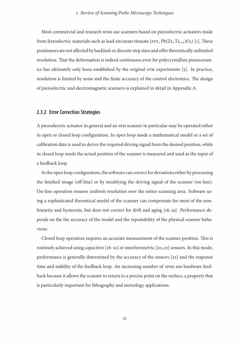
2.3.2 Error Correction Strategies
A piezoelectric actuator in general and an spm scanner in particular may be operated either
in open or closed loop con�guration. In open loop mode a mathematical model or a set of
calibration data is used to derive the required driving signal from the desired position, while
in closed loop mode the actual position of the scanner is measured and used as the input of
a feedback loop.
In the open loop con�guration, the so ware can correct for deviations either by processing
the �nished image (o�-line) or by modifying the driving signal of the scanner (on-line).
On-line operation ensures uniform resolution over the entire scanning area. So ware us-
ing a sophisticated theoretical model of the scanner can compensate for most of the non-
linearity and hysteresis, but does not correct for dri and aging [18, 19]. Performance de-
pends on the the accuracy of the model and the repeatability of the physical scanner beha-
viour.
Closed loop operation requires an accurate measurement of the scanner position. ¿is is
routinely achieved using capacitive [18–21] or interferometric [20,22] sensors. In this mode,
performance is generally determined by the accuracy of the sensors [22] and the response
time and stability of the feedback loop. An increasing number of spms use hardware feed-
back because it allows the scanner to return to a precise point on the surface, a property that
is particularly important for lithography and metrology applications.
21
2 Review of Scanning Probe Microscopy Techniques
¿ehysteresis of a piezoelectric positioner can also be reduced by using the charge instead
of the voltage as the controlling parameter [20, 23]. ¿is approach may be combined with
other error compensation strategies, but reduces the e�ective resolution of the actuator [18].
For scanner designs that do not rely on the linearity of the piezoelectric e�ect, which
changes its sign if the electric �eld is reversed, electrostrictive materials are a viable altern-
ative [20]. Electrostriction is a property of all dielectrics, which deform in proportion to the
square of the external electric �eld. Because of its strong electrostrictive response, themater-
ial most widely used for actuators is leadmagnesium niobate (pmn, Pb(Mg~Nb~)O) [24].
pmn exhibits less creep and hysteresis than pzt, but has a stronger temperature dependence
and smaller range for similarly sized actuators. In practice, its use in spm scanners is limited
to applications where control of the hysteresis is crucial, such as force-distance measure-
ments [20].
2.4 A Closer Look at Scanning Force Microscopy
2.4.1 Overview
In this section I shall explain the operation of scanning force microscopes in more detail.
Naturally, special attention is given to the atomic force microscope, and the various ways of
functionalizing the tip of an sfm or using it as an enabling technology for other microscopy
methods are not covered.
sfms use the de�ection or resonant frequency of a cantilever as a measure of the tip–
sample interaction. ¿e de�ection of the probe must be measured with su�cient accuracy
to achieve the desired resolution, and Sec. 2.4.3 compares various approaches to this problem.
¿e dynamic force microscope expounded in Sec. 2.4.5 vibrates its probe, and the frequency
response is determined; otherwise, the interaction force is recorded directly in a static force
measurement.
From Latin stringere, ‘to draw tight’
22
2 Review of Scanning Probe Microscopy Techniques
In Sec. 2.4.6 I shall brie�y touch on the capability of afm for atomic resolution imaging.
While not germane to the experiments reported in this thesis, this serves to illustrate the
versatility of the technique and puts it in the context of the development of spms in general.
Finally, in Sec. 2.4.8 the origins of artefacts in afm images are discussed, which will allow the
reader to better understand the afm images presented in this thesis and follow the discussion
in Chapter 3.
2.4.2 The Probe
As shown in Fig. 2.2, an sfm probe consists of a sensing tip attached to the end of a �ex-
ible cantilever. Nowadays, a large range of probes for di�erent applications is commercially
available. ¿e tip is characterized by its shape as well as its electrical, chemical, and mech-
anical properties. It is manufactured from a crystalline material by mechanical crushing, or,
more commonly, chemical etching. ¿e tip angle determines the ability of the probe to follow
rough surfaces exhibiting features with high aspect ratios. ¿e tip radius limits the resolution
of measurements using long-range forces. Silicon tips with tip angles of approximately 10Xand radii of curvature of 20nm are readily available. Even sharper tips are possible for spe-
cialized applications. For electrochemical applications, electronic measurements, and dfm
measurements in the presence of a bias voltage, tips must be conducting. ¿is o en means
heavily doped semiconductors or metal coatings, but for conduction measurements solid
metal tips may be required. For mechanical surface modi�cation, diamond tips can be used.
¿e elastic deformation of the cantilever bearing the tip is used tomeasure the tip–sample
interaction. ¿e de�ection z is approximately proportional to the applied force Fts:
Fts � kz, (2.4)
where k is the sti�ness of the cantilever. For a rectangular beam,
k � Etw
4�ℓ� ∆ℓ� , (2.5)
23
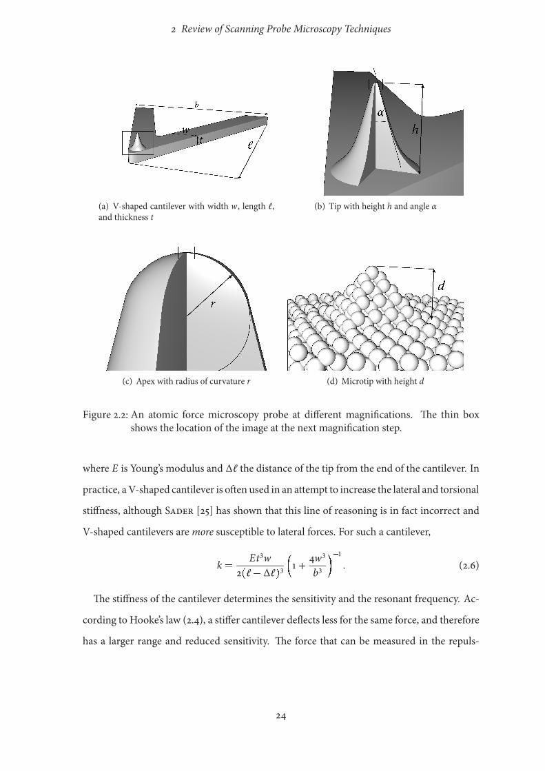
2 Review of Scanning Probe Microscopy Techniques
(a) V-shaped cantilever with width w, length ℓ,and thickness t
(b) Tip with height h and angle α
(c) Apex with radius of curvature r (d) Microtip with height d
Figure 2.2: An atomic force microscopy probe at di�erent magni�cations. ¿e thin boxshows the location of the image at the next magni�cation step.
where E is Young’s modulus and ∆ℓ the distance of the tip from the end of the cantilever. In
practice, aV-shaped cantilever is o en used in an attempt to increase the lateral and torsional
sti�ness, although Sader [25] has shown that this line of reasoning is in fact incorrect and
V-shaped cantilevers aremore susceptible to lateral forces. For such a cantilever,
k � Etw
2�ℓ� ∆ℓ� �1� 4w
b��
. (2.6)
¿e sti�ness of the cantilever determines the sensitivity and the resonant frequency. Ac-
cording to Hooke’s law (2.4), a sti�er cantilever de�ects less for the same force, and therefore
has a larger range and reduced sensitivity. ¿e force that can be measured in the repuls-
24
2 Review of Scanning Probe Microscopy Techniques
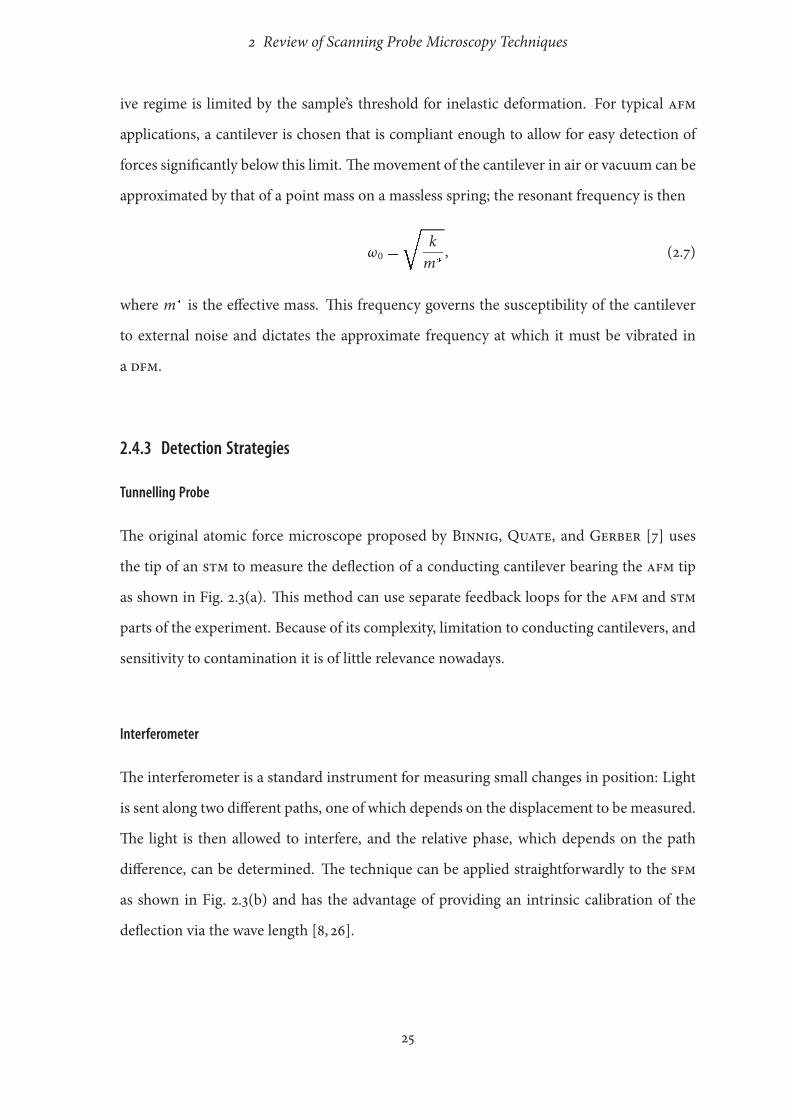
ive regime is limited by the sample’s threshold for inelastic deformation. For typical afm
applications, a cantilever is chosen that is compliant enough to allow for easy detection of
forces signi�cantly below this limit. ¿emovement of the cantilever in air or vacuum can be
approximated by that of a point mass on a massless spring; the resonant frequency is then
ω �¾k
m� , (2.7)
where m� is the e�ective mass. ¿is frequency governs the susceptibility of the cantilever
to external noise and dictates the approximate frequency at which it must be vibrated in
a dfm.
2.4.3 Detection Strategies
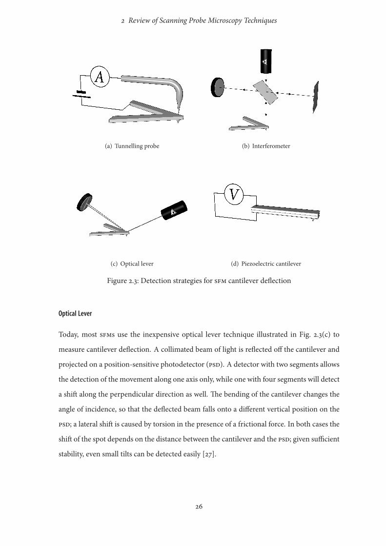
Tunnelling Probe
¿e original atomic force microscope proposed by Binnig, Quate, and Gerber [7] uses
the tip of an stm to measure the de�ection of a conducting cantilever bearing the afm tip
as shown in Fig. 2.3(a). ¿is method can use separate feedback loops for the afm and stm
parts of the experiment. Because of its complexity, limitation to conducting cantilevers, and
sensitivity to contamination it is of little relevance nowadays.
Interferometer
¿e interferometer is a standard instrument for measuring small changes in position: Light
is sent along two di�erent paths, one of which depends on the displacement to be measured.
¿e light is then allowed to interfere, and the relative phase, which depends on the path
di�erence, can be determined. ¿e technique can be applied straightforwardly to the sfm
as shown in Fig. 2.3(b) and has the advantage of providing an intrinsic calibration of the
de�ection via the wave length [8, 26].
25
2 Review of Scanning Probe Microscopy Techniques
(a) Tunnelling probe (b) Interferometer
(c) Optical lever (d) Piezoelectric cantilever
Figure 2.3: Detection strategies for sfm cantilever de�ection
Optical Lever
Today, most sfms use the inexpensive optical lever technique illustrated in Fig. 2.3(c) to
measure cantilever de�ection. A collimated beam of light is re�ected o� the cantilever and
projected on a position-sensitive photodetector (psd). A detector with two segments allows
the detection of the movement along one axis only, while one with four segments will detect
a shi along the perpendicular direction as well. ¿e bending of the cantilever changes the
angle of incidence, so that the de�ected beam falls onto a di�erent vertical position on the
psd; a lateral shi is caused by torsion in the presence of a frictional force. In both cases the
shi of the spot depends on the distance between the cantilever and the psd; given su�cient
stability, even small tilts can be detected easily [27].
26
2 Review of Scanning Probe Microscopy Techniques
¿is method was known long before the sfm existed, being used in early pro�lometers
which are conceptually similar to afms but operate at much lower resolution. Instead of
a psd, these instruments used a moving strip of photographic �lm, on which a magni�ed
representation of the sample pro�le would be traced by the re�ected beam.
Piezoelectric Cantilever
Fig. 2.3(d) shows how the de�ection can bemeasured directly by using a cantilever built from
a piezoelectric unimorph or bimorph sensor (see Section A.1.4). As no external detection
mechanism is required, the complexity of the instrument is reduced. However, fabricating
and changing the cantilevers is more di�cult and expensive. Piezoelectric detection is par-
ticularly interesting for applications where an external detection mechanism is di�cult to
implement because of limited space or accessibility [28, 29].
2.4.4 Tip–Sample Interaction in the Atomic Force Microscope
The Problem
In contrast to the stm, there is in general no useful approximation such as Eq. (2.1) for the
force between the tip of an afm and the sample. Instead, the potential has contributions
from di�erent interactions. Some of these contributions decay more slowly than the tunnel
current, so that themacroscopic shape of the tip and themedium play an important role and
a purely local model may be insu�cient to predict the force on the tip. Even so, short-rage
forces between the atoms at the tip apex and the sample may still enable atomic resolution.
Especially when operating in the repulsive regime, the interaction force can be high enough
that the elastic deformation of the tip and the sample must also be taken into account [20].
For topographic measurements at the scale of several nanometres and above, these com-
plications can o en be ignored, but understanding contrast at the atomic scale and between
di�erent materials depends on a realistic model of these forces.
27
2 Review of Scanning Probe Microscopy Techniques
�
� � �
V/E
d/d
repuls. attractive
E �� ddǑ � � d
dǑ�
(a) Example potential with attractive and repulsiveparts
���
� � �F/�E /d
�
d/d
α
α�a
β
β�b
Ed
�� ddǑ � � d
dǑ�
(b) Interaction force corresponding to the potentialin (a). Straight lines represent the elastic force of thecantilever.
Figure 2.4: Features of the tip–sample interaction in an afm.
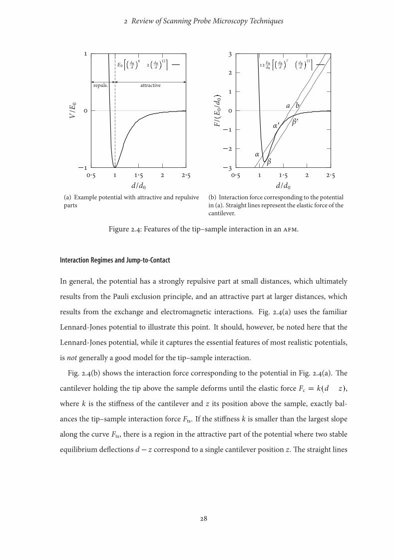
Interaction Regimes and Jump-to-Contact
In general, the potential has a strongly repulsive part at small distances, which ultimately
results from the Pauli exclusion principle, and an attractive part at larger distances, which
results from the exchange and electromagnetic interactions. Fig. 2.4(a) uses the familiar
Lennard-Jones potential to illustrate this point. It should, however, be noted here that the
Lennard-Jones potential, while it captures the essential features of most realistic potentials,
is not generally a good model for the tip–sample interaction.
Fig. 2.4(b) shows the interaction force corresponding to the potential in Fig. 2.4(a). ¿e
cantilever holding the tip above the sample deforms until the elastic force Fc � k�d � z�,where k is the sti�ness of the cantilever and z its position above the sample, exactly bal-
ances the tip–sample interaction force Fts. If the sti�ness k is smaller than the largest slope
along the curve Fts, there is a region in the attractive part of the potential where two stable
equilibrium de�ections d � z correspond to a single cantilever position z. ¿e straight lines
28
2 Review of Scanning Probe Microscopy Techniques
in Fig. 2.4(b) correspond to the elastic force of a cantilever at the two positions z � a and
z � b delimiting this range; the two points where the forces balance are marked α (β) and
α� (β�); for cantilever positions between a and b, there is a third (metastable) point whereFc � Fts. When the probe approaches the surface, the de�ection increases continuously un-
til it reaches a, where the de�ection increases suddenly and the tip jumps from the position
corresponding to α� to that corresponding to α. During retraction the de�ection changescontinuously until the cantilever reaches b, where the tip jumps from β to β�. Consequently,the interaction force measured as a function of the cantilever position z shows discontinu-
ities and hysteresis; the part of the force-distance curve between α� and β is never sampled.¿e two discontinuities are known as ‘jump-to-contact’ and ‘jump-o�-contact’, respectively.
¿ey can only be avoided by increasing k, which leads to smaller de�ections and a lower
signal-to-noise ratio [20, 28].
Important Contributions to the Tip–Sample Interaction
Under ambient conditions, many surfaces including oxidized semiconductor surfaces are
covered by a thin layer of adsorbed water [20, 26]. Once the water layers on the tip and the
surface touch, a meniscus is formed and the surface tension pulls the tip towards the sample.
¿e in�uence of the water layer is small before the meniscus forms, but once it has formed,
it dominates the interaction, extending far from the sample as the meniscus is stretched.
¿e magnitude of the meniscus force is a complicated function of the distance and depends
on the shape of the tip; for large d Q r it varies approximately as 1~d until the meniscusruptures [20].
At large distances and in the absence of a meniscus force, the interaction is dominated by
the van derWaals force. ¿is force results fromelectromagnetic dipole interactions. Between
individual atoms or molecules, all contributions to the van derWaals force vary as 1~d. It is
generally attractive, but can become repulsive in densemedia. ¿e situation ismore complic-
29
2 Review of Scanning Probe Microscopy Techniques
ated for macroscopic bodies. Assuming isotropy and additivity, the force between a surface
and a sphere of radius r at a distance dP r is approximately proportional to d~r [20, 30].If there is a voltage di�erence between the tip and the sample, an attractive Coulomb force
pulls them together. For a tip with radius of curvature r, the force varies with distance as 1~dif rQ d and as 1~d if rP d [20]. If the tip or the sample are conducting, image forces have
to be considered as well. For topographic measurements at the nanometre scale and above,
the force caused by an intentional bias can be used to improve the stability of a dynamic force
microscope [26].
Chemical forces result from the interaction of the electron clouds and nuclei at the apex
of the tip with those at the sample surface. ¿ey are the same forces that are responsible for
covalent and hydrogen bonds and cause the repulsion that is measured in contact afm. ¿e
attractive part of the potential decays very rapidly with distance, and it is this behaviour that
enables atomic resolution in an afm, since it means that only the microtip coming closest to
the sample contributes signi�cantly to the interaction [11, 12].
2.4.5 Dynamic Force Microscopy
Mechanism
A dfm is an sfm in which the cantilever and tip system is vibrated close to a resonant fre-
quency, usually using a piezoelectric transducer. ¿e dynamic behaviour of the cantilever
changes as a result of the tip–sample interaction, and it is this change that is measured and
used to form an image. ¿e original afm by Binnig et al. already included dynamic force
capabilities [7], but static forcemeasurements were found to bemore reliable. ¿e �rst work-
ingdfmwas demonstrated byMartin et al. [8] in 1987. Compared to static forcemicroscopy,
dfm is more suitable for measurements in the attractive region of the tip–sample potential
and avoids jump-to-contact. ¿e signal-to-noise ratio can be improved by using narrow-
band detection in combination with a standard lock-in technique [28].
30
2 Review of Scanning Probe Microscopy Techniques
The Frequency Shift
¿e motion of the cantilever can be approximated by that of a point mass on a massless
harmonic spring [11, 30, 31]. In the presence of a tip–sample interaction force Fts�z� and adriving force Fext�t� � F cos�ωt� the equation of motion is
m�z � 2γm�z � k �z � z� � Fts�z�� Fext�t�, (2.8)
wherem� is the e�ectivemass, γ the damping coe�cient, and k the sti�ness. If the amplitudeof the oscillation is small compared to the distance over which Fts�z� changes, Fts�z� ��z � z�F �ts�z�. For realistic long range interaction forces, this approximation is valid if theamplitude A is much smaller than the distance of closest approach D; for general forces, the
required Amay be arbitrarily small [32, 33]. Eq. (2.8) then becomes
m�z � 2γm�z � �k � F �ts�z�� �z � z� � Fext�t�. (2.9)
¿is is just the equation of a forced harmonic oscillator with an e�ective spring constant
k� def� k � F �ts�z� and the resonant (angular) frequency isω �¾
k�m� �¾
k � F �ts�z�m� . (2.10)
¿e frequency shi due to the interaction between the tip and the sample is hence
∆ω �¾k
m� �¾k � F �ts�z�
m� � �F �ts�z�2k
ω (2.11)
for F �ts�z�P k [8,26,28]. An image taken at constant frequency shi ∆ω therefore corres-
ponds to a surface of constant force gradient F �ts. In practice, however, the condition AP D
is not ful�lled in many dfm experiments [32, 33].
Schwarz et al. [33] suggest a di�erent approach that approximates the true anharmonic
potential by two harmonic potentials and is valid for AQ D, provided the decay length λ of
the tip–sample interaction is much smaller than A. In this theory, the frequency shi obeys
∆ω � Vts�D�ºλ
, (2.12)
¿is is a reasonable approximation for cantilevers in vacuo but increasingly less so as hydrodynamic e�ectsbecome more important in more viscous media.
31
2 Review of Scanning Probe Microscopy Techniques
where Vts�D� is the tip–sample interaction potential at the point of closest approach and λthe range of the interaction. It can be understood intuitively that the potential at the point
of closest approach dominates the e�ect: ¿e tip has its lowest speed there and experiences
the potential for a longer time; since λP A, the interaction is negligible at the other turning
point [11, 33].
To arrive at a more accurate understanding of the tip dynamics, comparison with simu-
lations from a realistic model of the tip–sample interaction is required and the behaviour of
the feedback system determining Fext has to be taken into account.
Amplitude Modulation
In amplitude modulation afm (am-afm), the cantilever is excited at a constant frequency.
¿e detection mechanism is used to measure the change in the amplitude response caused
by the shi in the resonant frequency due to the interaction of the tip with the sample. ¿e
amplitude is either recorded directly or kept constant using a feedback loop [8, 30, 31, 33]. In
this mode, further spectroscopic information may be obtained by measuring the phase shi
between the excitation signal and the cantilever vibration [30].
Frequency Modulation
¿e alternative approach is frequency modulation afm (fm-afm), which uses a second,
faster feedback loop to keep the measured amplitude constant by varying the excitation fre-
quency and amplitude. ¿is way, the shi in the resonance frequency can be measured dir-
ectly; the excitation amplitude contains information about energy transfer to the sample [30,
31, 33, 34]. fm-afm is preferable to am-afm under high vacuum conditions, because the ab-
sence of a damping medium implies a very high quality factor and the oscillation amplitude
responds slowly to a change in the resonant frequency [34].
Dynamic Force Microscopy in a Liquid
dfm in a liquid is interesting because it is required to observe many biological samples and
potentially allows atomic resolution. Modelling the dynamics is more involved, because the
32
2 Review of Scanning Probe Microscopy Techniques
movement of the liquid between the cantilever and the sample becomes important and the
probe can no longer be approximated by a mass on a spring [30, 35]. Compared to the same
cantilever in air or vacuum, there are more and broader resonances at lower frequencies [30]
and the quality factor decreases by two orders of magnitude. ¿e latter problem can be
overcome by using a positive feedback loop to drive the oscillation [36].
2.4.6 True Atomic Resolution
Like the stm, the afm can in principle achieve atomic resolution [12, 28, 33, 35]. In practice,
this goal is considerably harder to achieve, since important contributions to the tip–sample
interaction decay slowly. However, only short-range chemical forces can be used for imaging
at the atomic scale. Sharp tips are necessary to reduce the contribution of the van der Waals
force [28]. In air, themeniscus force dominates the interaction; measurementsmust hence be
taken in a liquid [35,37] or in uhv [28,33]. While the repulsive forces used in contact afm are
short range and images with correct atomic spacings have been obtained this way, the forces
on typical tips in contact mode are too large to be supported by a single microtip, preventing
true atomic resolution [28, 33]. Additionally, the atomically clean surfaces of many tips and
samples can stick together under uhv conditions by forming chemical bonds [28]. Atomic
resolution images in uhv have only been obtained by large amplitude dfm, which prevents
sticking and jump-to-contact. As with the stm, atomic resolution imaging ofmanymaterials
may call for elaborate sample preparation, which can in itself require working in uhv.
2.4.7 Contact, Non-Contact, and Tapping Mode
In the literature the operating mode of a force microscope is o en characterized as contact,
non-contact (ncm), or tapping mode. In contact mode the repulsive part of the surface po-
tential is probed. ¿is is the usual situation for static forcemeasurements, for which themain
feedback loop is set up to increase the tip-sample distance when the detected force increases.
Non-contact mode refers to operation in the attractive part of the potential. ¿is regime is
33
2 Review of Scanning Probe Microscopy Techniques
usually associated with dynamic force microscopy, which allows for increased sensitivity in
detecting small attractive forces and prevents jump-to-contact. Finally, tapping mode des-
ignates a dfm experiment in which the tip samples the attractive part of the potential for
most of its oscillation cycle but penetrates into the repulsive part on closest approach to the
sample. In practice distinguishing between non-contact and tapping modes in dfm experi-
ments may be di�cult and requires a detailed understanding of the tip-sample interaction.
fm-afm is o en identi�ed with ncm and am-afm with tapping mode [30, 31]; this usage
frequently, but by no means necessarily agrees with the straightforward de�nitions given
here.
2.4.8 Artefacts in Atomic Force Microscope Images
Finite Tip Size
As shown in Fig. 2.2(b), real afm tips have a �nite radius of curvature r and angle α. When
scanning sample features with high aspect ratios, the point of contact is not always at the
apex of the tip. Consequently, such structures cannot be traced accurately. ¿is e�ect is
illustrated in Fig. 2.5: ¿e lateral size of small features is overestimated, while the tip cannot
reach the bottom of deep holes or trenches. Vertical sidewalls are imaged with rounded or
slanted pro�les, depending on the shape of the tip at the scale of the feature. Artefacts due to
�nite tip size can usually be distinguished from sample features by the fact that they do not
change their orientation when the sample is rotated relative to the tip. ¿ey o en appear as
the repetition of a pattern that corresponds to the shape of the tip apex.
If the surface of the sample is given by S�x , y� and the surface of the tip by T�x , y�, theimage or apparent sample surface is
S��x , y� � �minξ,η>Z
�T�ξ � x , η� y�� S�ξ, η�� . (2.13)
At each point �x , y�, the minimal distance between the entire shi ed tip T�ξ�x , η� y� and
34
2 Review of Scanning Probe Microscopy Techniques
(a) Measurement using a tip with �nite radius r (b) Apparent topography measured in (a)
(c) Measurement using a tip with �nite angle α (d) Apparent topography measured in (c)
Figure 2.5: Finite tip size e�ects in an afm measurement. Arrows indicate the trajectory ofthe centre of curvature of the tip.
the entire sample surface S�ξ, η� determines the distance by which the tip can be loweredtowards the sample before contact is established.
For a known tip shape and surface Eq. (2.13) allows a straightforward numerical simu-
lation of the expected image. Villarrubia [38] has developed a formulation in terms of
mathematical morphology and used it to show that the operation can be reversed: Given the
shape of the tip and the image, the sample surface can be recovered. ¿e reconstruction is
exact where the surface has been in contact with the tip and provides an upper bound else-
where. Similarly, the tip can be reconstructed by the same method if the sample geometry is
known.
35
2 Review of Scanning Probe Microscopy Techniques
In practice, the reconstruction of images is hampered by the fact that the shape of the tip
apex is usually not well de�ned, as it can change during operation—even if care is taken to
assess the speci�c probe by imaging a characterizer or by other means. If the tip is known to
be su�ciently sharp that its area of interaction with the sample is much smaller than a given
image, this image can be used to estimate the current shape of the tip via a self-consistent
iterative ‘blind reconstruction’ method [38].
For the idealized �nite size tip shown in Fig. 2.2(b) and surface features with simple geo-
metries, closed expressions for the imaging error can be obtained in many cases by a simple
geometrical construction; such expressions can be useful in the quick assessment of afm
images. A mesa with a rectangular cross-section of width w and height h, when imaged us-
ing a tip of �nite radius of curvature r C h—Fig. 2.5(a) and (b)—produces an image with
apparent width
w� � w � 2º2rh � h. (2.14)
If a hole or groove is imaged with a tip that cannot reach its bottom as in Fig. 2.5(c) and (d),
the apparent depth of the feature is given by
h� � w
2cot α (2.15)
for a tip with a sharp point. If a �nite radius of curvature r �A h is taken into account, the
length of the tip is reduced, and Eq. (2.15) becomes
h� � w
2cot α � r�csc α � 1�. (2.16)
Other Effects
afms are naturally susceptible to artefacts a�ecting all spms, such as scanner nonlinearity,
smoothing and overshoot due to the �nite response time of the feedback loop, and narrow-
band noise mimicking a periodic surface structure. Speci�cally in an afm, the tip can mo-
mentarily stick to the surface and then jump o�, resulting in a spike in the image that does
not correspond to a sample feature. In a dfm, for some operating parameters there can be
36
2 Review of Scanning Probe Microscopy Techniques
two stable oscillation states corresponding to a single value of the tip–sample force [30]. In
this case, the apparent topography can jump between two levels with an approximately con-
stant o�set between them. ¿e jumps are usually random, but can sometimes mimic a step
in the sample.
2.5 Scanning-Probe-Based Lithography
2.5.1 Manipulation of Individual Atoms
A famous example of the ability of the spm to shape matter at an atomic scale is the ‘quantum
corral’ of iron atoms on a copper surface created by Crommie et al. [39] via the controlled
movement of adatoms using an stm. ¿e sensitivity of the stm to the local electronic density
of states has been used to image the standing wave corresponding to an electron trapped in
the arti�cial enclosure.
In order to manipulate individual atoms, the stm must operate under uhv, which is re-
quired for atomic resolution imaging. Performing the experiment at liquid helium temperat-
ures improves the stability andmay be necessary to prevent di�usion of the adatoms. ¿e tip
can be used to move individual atoms either in a parallel process, in which the connection
to the surface is never broken, or in a perpendicular process, in which the atom detaches
from the surface and is adsorbed at the tip. In the parallel process, the electric �eld at the
apex of the tip can be increased to enhance di�usion in the desired direction. Alternatively,
the tip can be lowered towards an adatom by changing the feedback parameter until the
chemical forces allow for sliding the atom across the surface. ¿e perpendicular process
transfers atoms between the surface and the tip by approaching and retracting the probe or
by applying a voltage pulse to overcome the potential barrier [40].
2.5.2 Nanoindentation
afms can also be used to modify a sample mechanically. ¿e tip is pressed against the work-
piece with a force exceeding the threshold for inelastic deformation and indents or chips the
37
2 Review of Scanning Probe Microscopy Techniques
surface. It must be attached to a su�ciently sti� cantilever to support the interaction force
and commonly consists of a hard material, e.g., diamond, to minimize wear. Apart from the
sharpness and durability of the tip, the performance of this method depends critically on the
mechanical properties of the sample itself; under optimal conditions, a resolution of 10nm
can be realized [41,42]. Since high resolutionmodi�cations can only be achievedwith certain
substrates, a separate surface layer consisting of a so polymer, metal, or oxide is sometimes
applied and the pattern transferred using an auxiliary etch technique. Nanoscratching with
an oscillating force as in a dfm helps avoid sticking of the tip [41, 43, 44].
2.5.3 Electrical and Optical Surface Modification
A voltage pulse applied to a conducting stm or afm tip can modify the substrate in vari-
ous other ways. Field emission from an stm tip can be used to expose organic resists at
length scales comparable with the best electron beam writers. Joule heating due to local
high current densities and �eld-assisted evaporation have been proposed as mechanisms for
the surface modi�cation observed in some experiments. ¿e electrical �eld in the vicinity of
an stm or afm tip can activate the chemical vapour deposition (cvd) of some materials, es-
pecially metals. Finally, the voltage di�erence can be used to locally enable electrochemical
processes [42]. A special case of the latter technique is the local anodic oxidation of metal
or semiconductor surfaces using adsorbed water as the electrolyte, which is discussed in
more detail in Chapter 3. Similar to the situation with nanoindentation, these methods crit-
ically depend on the chemical and electrical properties of the involved materials; sometimes
an additional pattern transfer process can circumvent this limitation. Optical techniques
include the exposure of conventional photoresist and other photoactive surfaces by illumin-
ation mode nfsom.
2.6 Summary
¿e spm is a versatile tool that can measure and manipulate a surface at length scales from
fractions of an Ångström up to several microns. ¿e concept can be used with a large range
38
Bibliography
of di�erent tip–sample interactions, andmany di�erent physical properties of the sample can
be mapped. Advances in scanner and noise control technology mean that the fundamental
limit to the resolution of an spm method is determined by the size and shape of the probe
and the range of the interaction it uses. Correct interpretation of images requires a detailed
understanding of this interaction at the relevant scale.
Bibliography
[1] E. T. Yu. Nanoscale characterization of semiconductor materials and devices usingscanning probe techniques. Materials Science and Engineering, R17:147–206, 1996.
[2] G. Schmalz. Über Glätte und Ebenheit as physikalisches und physiologisches Problem.Zeitschri des Verbandes Deutscher Ingenieure, 73:144–161, October 1929.
[3] R. Young, J. Ward, and F. Scire. Observation of metal-vacuum-metal tunneling, �eldemission, and the transition region. Physical Review Letters, 27(14):922–924, October1971.
[4] R. Young, J. Ward, and F. Scire. ¿e topographiner: An instrument for measuringsurface microtopography. Review of Scienti�c Instruments, 43(7):999–1011, July 1972.
[5] G. Binnig and H. Rohrer. Scanning tunneling microscopy—from birth to adolescence.Reviews of Modern Physics, 59(3):615–625, July 1987. Nobel Lecture.
[6] G. Binnig, H. Rohrer, C. Gerber, and E. Weibel. Surface studies by scanning tunnelingmicroscopy. Physical Review Letters, 49(1):57–61, July 1982.
[7] G. Binnig, C. F. Quate, and C. Gerber. Atomic force microscope. Physical ReviewLetters, 56(9):930–933, March 1986.
[8] Y. Martin, C. C. Williams, and H. K. Wickramasinghe. Atomic force microscope-forcemapping and pro�ling on a sub-100Å scale. Journal of Applied Physics, 61(10):4723–4729, May 1987.
[9] U. Dürig, D. W. Pohl, and F. Rohner. Near-�eld optical-scanning microscopy. Journalof Applied Physics, 59(10):3318–3327, May 1986.
[10] R. C. Reddick, R. J. Warmack, and T. L. Ferrell. New form of scanning optical micro-scopy. Physical Review A, 39(1):767–770, January 1989.
[11] D. Drakova. ¿eoretical modelling of scanning tunnelling microscopy, scanning tun-nelling spectroscopy and atomic force microscopy. Reports on Progress in Physics,64:205–290, 2001.
39
Bibliography
[12] W. A. Hofer, A. S. Foster, and A. L. Shluger. ¿eories of scanning probe microscopes atthe atomic scale. Reviews of Modern Physics, 75:1287–1331, October 2003.
[13] S. Gasiorowicz. Quantum Physics, chapter 5. John Wiley & Sons, New York, secondedition, 1996.
[14] J. Terso� and D. R. Hamann. ¿eory and application for the scanning tunneling mi-croscope. Physical Review Letters, 50(25):1998–2001, June 1993.
[15] J. G. Simmons. Generalized formula for the electric tunnel e�ect between similar elec-trodes separated by a thin insulating �lm. Journal of Applied Physics, 34(6):1793–1803,June 1963.
[16] C.Girard, C. Joachim, and S.Gauthier. ¿e physics of the near-�eld. Reports on Progressin Physics, 63:893–938, 2000. read 19th July 2005; C.
[17] J. W. P. Hsu. Near-�eld scanning optical microscopy studies of electronic and photonicmaterials and devices. Materials Science and Engineering, 33:1–50, 2001.
[18] J. E. Gri�th, G. L. Miller, C. A. Green, D. A. Grigg, and P. E. Russell. A scanningtunneling microscope with a capacitance-based position monitor. Journal of VaccumScience and Technology B, 8(6):2023–2027, November/December 1990.
[19] K. Dirscherl, J. Garnæs, and L. Nielsen. Modeling the hysteresis of a scanning probemicroscope. Journal of Vacuum Science and Technology B, 18(2), 621–625 2000.
[20] B. Cappella and G. Dietler. Force-distance curves by atomic force microscopy. SurfaceScience Reports, 34:1–104, 1999.
[21] L. Libioulle, A. Ronda, M. Taborelli, and J. M. Gilles. Deformations and nonlinearityin scanning tunneling microscope images. Journal of Vacuum Science and TechnologyB, 9(2):655–658, March/April 1991.
[22] H.-C. Yeh, W.-T. Ni, and S.-S. Pan. Digital closed-loop nanopositioning using recti-linear �exure stage and laser interferometry. Control Engineering Practice, 13:559–566,2005.
[23] K. R. Koops, P. M. L. O. Scholte, and W. L. de Koning. Observation of zero creep inpiezoelectric actuators. Applied Physics A, 68:691–697, 1999.
[24] L. E. Cross. Ferroelectric materials for electromechanical transducer applications. Ma-terials Chemistry and Physics, 43:108–115, 1996.
[25] J. E. Sader. Susceptibility of atomic forcemicroscope cantilevers to lateral forces. Reviewof Scienti�c Instruments, 74(4):2438–2443, April 2003.
[26] R. Erlandsson, G.M.McClelland, C.M.Mate, and S. Chiang. Atomic forcemicroscopyusing optical interferometry. Journal of Vacuum Science and Technology A, 6(2):266–270, March/April 1988.
40
Bibliography
[27] S. Alexander, L. Hellemans, O. Marti, J. Schneir, V. Elings, P. K. Hansma, M. Longmire,and J. Gurley. An atomic-resolution atomic-force microscope implemented using anoptical lever. Journal of Applied Physics, 65(1):164–167, January 1989.
[28] F. J. Giessibl. Atomic resolution of the silicon �111�-�7 � 7� surface by atomic forcemicroscopy. Science, 267(5194):68–71, January 1995.
[29] T. Akiyama, S. Gautsch, N. F. de Rooij, U. Staufer, P. Niedermann, L. Howald, D.Müller,A. Tonin, H.-R. Hidber, W. T. Pike, and M. H. Hecht. Atomic force microscope forplanetary applications. Sensors and Actuators A, 91:321–325, 2001.
[30] R. García and R. Pérez. Dynamic atomic force microscopy methods. Surface ScienceReports, 47:197–301, 2002.
[31] G. Couturier, R. Boisgard, L. Nony, and J. P. Aimé. Noncontact atomic force micro-scopy: Stability criterion and dynamical responses of the shi of frequency and damp-ing signal. Review of Scienti�c Instruments, 74(5):2726–2734, May 2003.
[32] H. Hölscher, U. D. Schwarz, and R. Wiesendanger. Calculation of the frequency shi in dynamic force microscopy. Applied Surface Science, 140:344–351, 1999.
[33] U. D. Schwarz, H. Hölscher, and R.Wiesendanger. Atomic resolution in scanning forcemicroscopy: Concepts, requirements, contrast mechanisms, and image interpretation.Physical Review B, 62(19):13089–13097, November 2000.
[34] R. Bennewitz, M. Bammerlin, M. Guggisberg, C. Loppacher, A. Barato, E. Meyer, andH.-J. Güntherodt. Aspects of dynamic force microscopy on NaCl/Cu(111): Resolution,tip–sample interactions and cantilever oscillation characteristics. Surface and InterfaceAnalysis, 27:462–466, 1999.
[35] F. M. Ohnesorge. Towards atomic resolution non-contact dynamic force microscopyin a liquid. Surface and Interface Analysis, 27:179–385, 1999.
[36] J. Tamayo, A. D. L. Humphris, R. J. Owen, and M. J. Miles. High-Q dynamic forcemicroscopy in liquid and its application to living cells. Biophysical Journal, 81:526–537,July 2001.
[37] F. M. Ohnesorge and G. Binnig. True atomic resolution by atomic force microscopythrough repulsive and attractive forces. Science, 360(5113):1451–1456, June 1993.
[38] J. S. Villarrubia. Algorithms for scanned probe microscope image simulation, surfacereconstruction, and tip estimation. Journal of Research of theNational Institute of Stand-ards and Technology, 102(4):425–454, July/August 1997.
[39] M. F. Crommie, C. P. Lutz, and D. M. Eigler. Con�nement of electrons to quantumcorrals on a metal surface. Science, 262(5131):218–220, October 1993.
41
Bibliography
[40] J. A. Stroscio and D. M. Eigler. Atomic and molecular manipulation with the scanningtunneling microscope. Science, 254(5036):1319–1326, November 1991.
[41] Y. Kim and C. M. Lieber. Machining oxide thin �lms with an atomic force microscope:Pattern and object formation on the nanometer scale. Science, 257:375–377, July 1992.
[42] R. M. Ny�enegger and R. M. Penner. Nanometer-scale surface modi�cation using thescanning probe microscope: Progress since 1991. Chemical Reviews, 97:1195–1230, 1997.
[43] M.Wendel, B. Irmer, J. Cortes, R. Kaiser, H. Lorenz, J. P. Kotthaus, A. Lorke, and E.Wil-liams. Nanolithography with an atomic forcemicroscope. Superlattices andMicrostruc-tures, 20(3):349–356, 1996.
[44] U. Kunze. Nanoscale devices fabricated by dynamic ploughing with an atomic forcemicroscope. Superlattices and Microstructures, 31(1):3–17, 2002.
42