18-Bit ADC with I2C Interface and Onboard Reference...
30
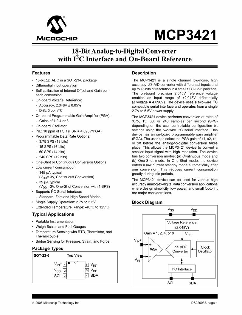
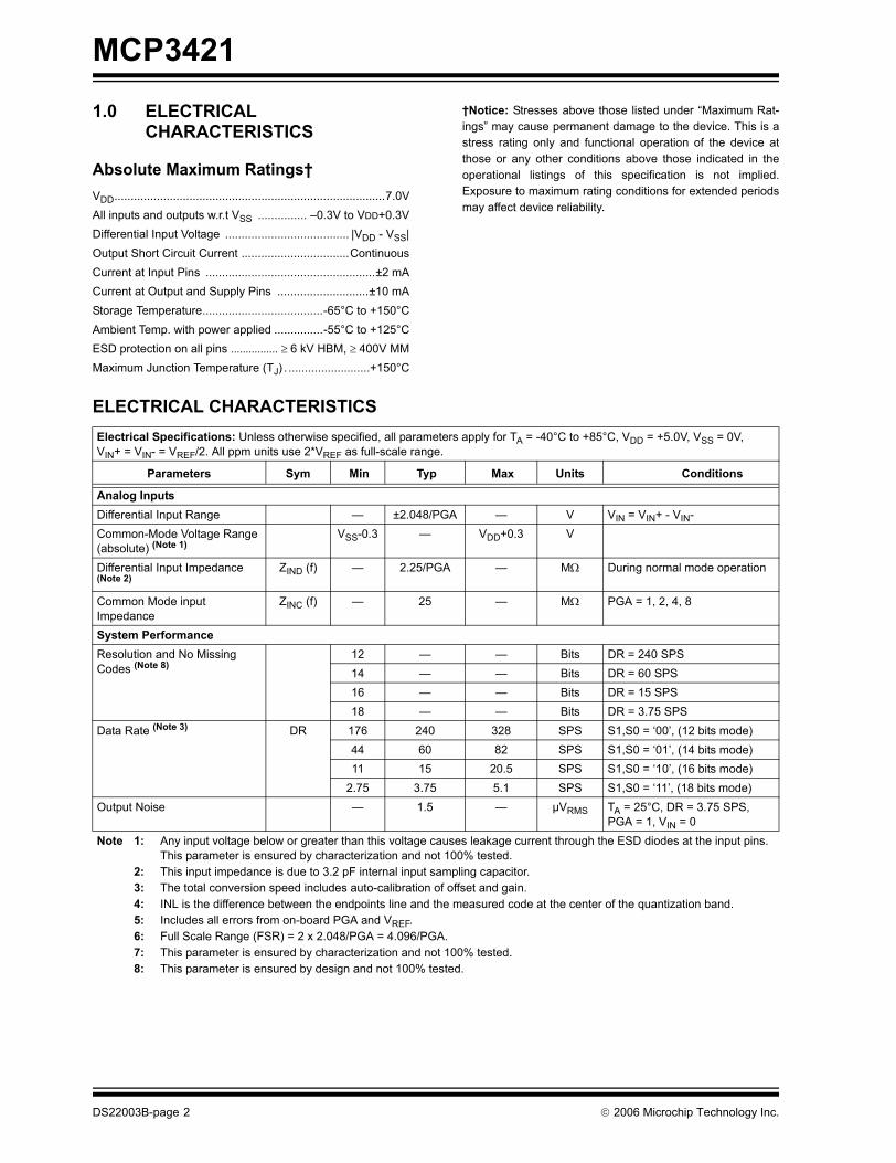
© 2006 Microchip Technology Inc. DS22003B-page 1 MCP3421 Features • 18-bit ΔΣ ADC in a SOT-23-6 package • Differential input operation • Self calibration of Internal Offset and Gain per each conversion • On-board Voltage Reference: - Accuracy: 2.048V ± 0.05% - Drift: 5 ppm/°C • On-board Programmable Gain Amplifier (PGA): - Gains of 1,2,4 or 8 • On-board Oscillator • INL: 10 ppm of FSR (FSR = 4.096V/PGA) • Programmable Data Rate Options: - 3.75 SPS (18 bits) - 15 SPS (16 bits) - 60 SPS (14 bits) - 240 SPS (12 bits) • One-Shot or Continuous Conversion Options • Low current consumption: - 145 μA typical (V DD = 3V, Continuous Conversion) - 39 μA typical (V DD = 3V, One-Shot Conversion with 1 SPS) • Supports I 2 C Serial Interface: - Standard, Fast and High Speed Modes • Single Supply Operation: 2.7V to 5.5V • Extended Temperature Range: -40°C to 125°C Typical Applications • Portable Instrumentation • Weigh Scales and Fuel Gauges • Temperature Sensing with RTD, Thermistor, and Thermocouple • Bridge Sensing for Pressure, Strain, and Force. Package Types Description The MCP3421 is a single channel low-noise, high accuracy ΔΣ A/D converter with differential inputs and up to 18 bits of resolution in a small SOT-23-6 package. The on-board precision 2.048V reference voltage enables an input range of ±2.048V differentially (Δ voltage = 4.096V). The device uses a two-wire I 2 C compatible serial interface and operates from a single 2.7V to 5.5V power supply. The MCP3421 device performs conversion at rates of 3.75, 15, 60, or 240 samples per second (SPS) depending on the user controllable configuration bit settings using the two-wire I 2 C serial interface. This device has an on-board programmable gain amplifier (PGA). The user can select the PGA gain of x1, x2, x4, or x8 before the analog-to-digital conversion takes place. This allows the MCP3421 device to convert a smaller input signal with high resolution. The device has two conversion modes: (a) Continuous mode and (b) One-Shot mode. In One-Shot mode, the device enters a low current standby mode automatically after one conversion. This reduces current consumption greatly during idle periods. The MCP3421 device can be used for various high accuracy analog-to-digital data conversion applications where design simplicity, low power, and small footprint are major considerations. Block Diagram 1 2 3 4 5 6 V IN + V SS SCL V IN - V DD SDA Top View SOT-23-6 V SS V DD V IN + V IN - SCL SDA Voltage Reference Clock (2.048V) I 2 C Interface Gain = 1, 2, 4, or 8 V REF ΔΣ ADC Converter PGA Oscillator 18-Bit Analog-to-Digital Converter with I 2 C Interface and On-Board Reference
Transcript of 18-Bit ADC with I2C Interface and Onboard Reference...
MCP342118-Bit Analog-to-Digital Converter
with I2C Interface and On-Board Reference
Features• 18-bit ΔΣ ADC in a SOT-23-6 package• Differential input operation• Self calibration of Internal Offset and Gain per
each conversion• On-board Voltage Reference:
- Accuracy: 2.048V ± 0.05%- Drift: 5 ppm/°C
• On-board Programmable Gain Amplifier (PGA):- Gains of 1,2,4 or 8
• On-board Oscillator• INL: 10 ppm of FSR (FSR = 4.096V/PGA)• Programmable Data Rate Options:
- 3.75 SPS (18 bits)- 15 SPS (16 bits)- 60 SPS (14 bits)- 240 SPS (12 bits)
• One-Shot or Continuous Conversion Options• Low current consumption:
- 145 µA typical (VDD= 3V, Continuous Conversion)
- 39 µA typical(VDD= 3V, One-Shot Conversion with 1 SPS)
• Supports I2C Serial Interface:- Standard, Fast and High Speed Modes
• Single Supply Operation: 2.7V to 5.5V• Extended Temperature Range: -40°C to 125°C
Typical Applications• Portable Instrumentation• Weigh Scales and Fuel Gauges• Temperature Sensing with RTD, Thermistor, and
Thermocouple• Bridge Sensing for Pressure, Strain, and Force.
Package Types
DescriptionThe MCP3421 is a single channel low-noise, highaccuracy ΔΣ A/D converter with differential inputs andup to 18 bits of resolution in a small SOT-23-6 package.The on-board precision 2.048V reference voltageenables an input range of ±2.048V differentially(Δ voltage = 4.096V). The device uses a two-wire I2Ccompatible serial interface and operates from a single2.7V to 5.5V power supply.
The MCP3421 device performs conversion at rates of3.75, 15, 60, or 240 samples per second (SPS)depending on the user controllable configuration bitsettings using the two-wire I2C serial interface. Thisdevice has an on-board programmable gain amplifier(PGA). The user can select the PGA gain of x1, x2, x4,or x8 before the analog-to-digital conversion takesplace. This allows the MCP3421 device to convert asmaller input signal with high resolution. The devicehas two conversion modes: (a) Continuous mode and(b) One-Shot mode. In One-Shot mode, the deviceenters a low current standby mode automatically afterone conversion. This reduces current consumptiongreatly during idle periods.
The MCP3421 device can be used for various highaccuracy analog-to-digital data conversion applicationswhere design simplicity, low power, and small footprintare major considerations.
Block Diagram
1
2
3 4
5
6VIN+ VSSSCL
VIN-VDDSDA
Top ViewSOT-23-6
VSS VDD
VIN+
VIN-
SCL SDA
Voltage Reference
Clock
(2.048V)
I2C Interface
Gain = 1, 2, 4, or 8 VREF
ΔΣ ADCConverterPGA Oscillator
© 2006 Microchip Technology Inc. DS22003B-page 1
MCP3421
1.0 ELECTRICAL CHARACTERISTICS
Absolute Maximum Ratings†VDD...................................................................................7.0VAll inputs and outputs w.r.t VSS ............... –0.3V to VDD+0.3VDifferential Input Voltage ...................................... |VDD - VSS|Output Short Circuit Current .................................ContinuousCurrent at Input Pins ....................................................±2 mACurrent at Output and Supply Pins ............................±10 mAStorage Temperature.....................................-65°C to +150°CAmbient Temp. with power applied ...............-55°C to +125°CESD protection on all pins ................ ≥ 6 kV HBM, ≥ 400V MMMaximum Junction Temperature (TJ) . .........................+150°C
†Notice: Stresses above those listed under “Maximum Rat-ings” may cause permanent damage to the device. This is astress rating only and functional operation of the device atthose or any other conditions above those indicated in theoperational listings of this specification is not implied.Exposure to maximum rating conditions for extended periodsmay affect device reliability.
ELECTRICAL CHARACTERISTICSElectrical Specifications: Unless otherwise specified, all parameters apply for TA = -40°C to +85°C, VDD = +5.0V, VSS = 0V,VIN+ = VIN- = VREF/2. All ppm units use 2*VREF as full-scale range.
Parameters Sym Min Typ Max Units Conditions
Analog Inputs Differential Input Range — ±2.048/PGA — V VIN = VIN+ - VIN-Common-Mode Voltage Range (absolute) (Note 1)
VSS-0.3 — VDD+0.3 V
Differential Input Impedance (Note 2)
ZIND (f) — 2.25/PGA — MΩ During normal mode operation
Common Mode input Impedance
ZINC (f) — 25 — MΩ PGA = 1, 2, 4, 8
System PerformanceResolution and No Missing Codes (Note 8)
12 — — Bits DR = 240 SPS14 — — Bits DR = 60 SPS16 — — Bits DR = 15 SPS18 — — Bits DR = 3.75 SPS
Data Rate (Note 3) DR 176 240 328 SPS S1,S0 = ‘00’, (12 bits mode)44 60 82 SPS S1,S0 = ‘01’, (14 bits mode)11 15 20.5 SPS S1,S0 = ‘10’, (16 bits mode)
2.75 3.75 5.1 SPS S1,S0 = ‘11’, (18 bits mode)Output Noise — 1.5 — µVRMS TA = 25°C, DR = 3.75 SPS,
PGA = 1, VIN = 0 Note 1: Any input voltage below or greater than this voltage causes leakage current through the ESD diodes at the input pins.
This parameter is ensured by characterization and not 100% tested.2: This input impedance is due to 3.2 pF internal input sampling capacitor. 3: The total conversion speed includes auto-calibration of offset and gain.4: INL is the difference between the endpoints line and the measured code at the center of the quantization band.5: Includes all errors from on-board PGA and VREF.6: Full Scale Range (FSR) = 2 x 2.048/PGA = 4.096/PGA.7: This parameter is ensured by characterization and not 100% tested.8: This parameter is ensured by design and not 100% tested.
DS22003B-page 2 © 2006 Microchip Technology Inc.
MCP3421
Integral Nonlinearity (Note 4) INL — 10 35 ppm ofFSR
DR = 3.75 SPS(Note 6)
Internal Reference Voltage VREF — 2.048 — VGain Error (Note 5) — 0.05 0.35 % PGA = 1, DR = 3.75 SPSPGA Gain Error Match (Note 5) — 0.1 — % Between any 2 PGA gainsGain Error Drift (Note 5) — 5 40 ppm/°C PGA=1, DR=3.75 SPSOffset Error VOS — 15 40 µV Tested at PGA = 1
VDD = 5.0V and DR = 3.75 SPSOffset Drift vs. Temperature — 50 — nV/°C VDD = 5.0VCommon-Mode Rejection — 105 — dB at DC and PGA =1,
— 110 — dB at DC and PGA =8,TA = +25°C
Gain vs. VDD — 5 — ppm/V TA = +25°C, VDD = 2.7V to 5.5V,PGA = 1
Power Supply Rejection at DC — 100 — dB TA = +25°C, VDD = 2.7V to 5.5V,PGA = 1
Power RequirementsVoltage Range VDD 2.7 — 5.5 VSupply Current during Conversion
IDDA — 155 190 µA VDD = 5.0V— 145 — µA VDD = 3.0V
Supply Current during Standby Mode
IDDS — 0.1 0.5 µA
I2C Digital Inputs and Digital OutputsHigh level input voltage VIH 0.7 VDD — VDD VLow level input voltage VIL — — 0.3VDD VLow level output voltage VOL — — 0.4 V IOL = 3 mA, VDD = +5.0VHysteresis of Schmitt Trigger for inputs (Note 7)
VHYST 0.05VDD — — V fSCL = 100 kHz
Supply Current when I2C bus line is active
IDDB — — 10 µA
Input Leakage Current IILH — — 1 µA VIH = 5.5VIILL -1 — — µA VIL = GND
Pin Capacitance and I2C Bus CapacitancePin capacitance CPIN — — 10 pFI2C Bus Capacitance Cb — — 400 pFThermal CharacteristicsSpecified Temperature Range TA -40 — +85 °COperating Temperature Range TA -40 — +125 °CStorage Temperature Range TA -65 — +150 °C
ELECTRICAL CHARACTERISTICS (CONTINUED)Electrical Specifications: Unless otherwise specified, all parameters apply for TA = -40°C to +85°C, VDD = +5.0V, VSS = 0V,VIN+ = VIN- = VREF/2. All ppm units use 2*VREF as full-scale range.
Parameters Sym Min Typ Max Units Conditions
Note 1: Any input voltage below or greater than this voltage causes leakage current through the ESD diodes at the input pins.This parameter is ensured by characterization and not 100% tested.
2: This input impedance is due to 3.2 pF internal input sampling capacitor. 3: The total conversion speed includes auto-calibration of offset and gain.4: INL is the difference between the endpoints line and the measured code at the center of the quantization band.5: Includes all errors from on-board PGA and VREF.6: Full Scale Range (FSR) = 2 x 2.048/PGA = 4.096/PGA.7: This parameter is ensured by characterization and not 100% tested.8: This parameter is ensured by design and not 100% tested.
© 2006 Microchip Technology Inc. DS22003B-page 3
MCP3421
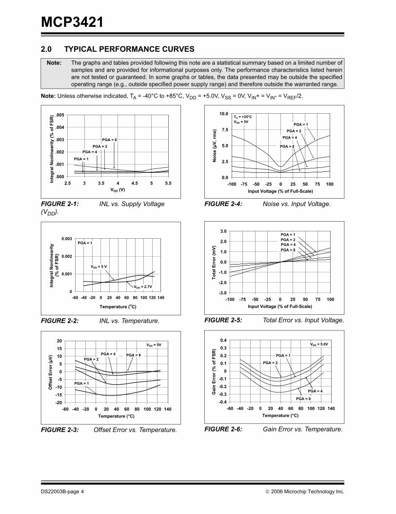
2.0 TYPICAL PERFORMANCE CURVES
Note: Unless otherwise indicated, TA = -40°C to +85°C, VDD = +5.0V, VSS = 0V, VIN+ = VIN- = VREF/2.
FIGURE 2-1: INL vs. Supply Voltage (VDD).
FIGURE 2-2: INL vs. Temperature.
FIGURE 2-3: Offset Error vs. Temperature.
FIGURE 2-4: Noise vs. Input Voltage.
FIGURE 2-5: Total Error vs. Input Voltage.
FIGURE 2-6: Gain Error vs. Temperature.
Note: The graphs and tables provided following this note are a statistical summary based on a limited number ofsamples and are provided for informational purposes only. The performance characteristics listed hereinare not tested or guaranteed. In some graphs or tables, the data presented may be outside the specifiedoperating range (e.g., outside specified power supply range) and therefore outside the warranted range.
.000
.001
.002
.003
.004
.005
2.5 3 3.5 4 4.5 5 5.5VDD (V)
PGA = 1
PGA = 2
PGA = 8
PGA = 4
Inte
gral
Non
linea
rity
(% o
f FSR
)
0
0.001
0.002
0.003
-60 -40 -20 0 20 40 60 80 100 120 140
Temperature (oC)
Inte
gral
Non
linea
rity
(% o
f FSR
)
VDD = 5 V
VDD = 2.7V
PGA = 1
-20
-15-10
-505
101520
-60 -40 -20 0 20 40 60 80 100 120 140Temperature (°C)
Offs
et E
rror
(µV)
VDD = 5V
PGA = 1
PGA = 2PGA = 8PGA = 4
0.0
2.5
5.0
7.5
10.0
-100 -75 -50 -25 0 25 50 75 100
Input Voltage (% of Full-Scale)
No
ise (
µV
, rm
s)
PGA = 1
PGA = 2
PGA = 8
PGA = 4
TA = +25°C
VDD = 5V
-3.0
-2.0
-1.0
0.0
1.0
2.0
3.0
-100 -75 -50 -25 0 25 50 75 100Input Voltage (% of Full-Scale)
Tota
l Err
or (m
V)
PGA = 1PGA = 2
PGA = 8PGA = 4
-0.4-0.3-0.2-0.1
00.10.20.30.4
-60 -40 -20 0 20 40 60 80 100 120 140Temperature (°C)
Gai
n Er
ror (
% o
f FSR
)
VDD = 5.0V
PGA = 1
PGA = 2
PGA = 8
PGA = 4
DS22003B-page 4 © 2006 Microchip Technology Inc.
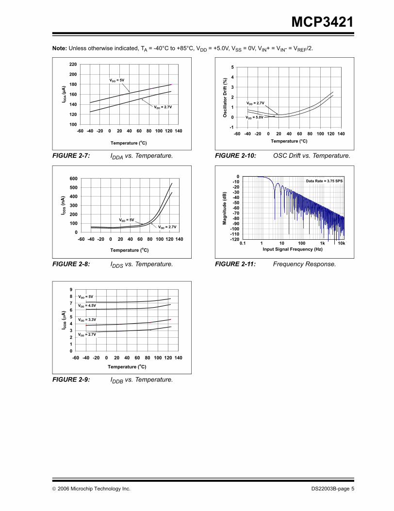
MCP3421
Note: Unless otherwise indicated, TA = -40°C to +85°C, VDD = +5.0V, VSS = 0V, VIN+ = VIN- = VREF/2.FIGURE 2-7: IDDA vs. Temperature.
FIGURE 2-8: IDDS vs. Temperature.
FIGURE 2-9: IDDB vs. Temperature.
FIGURE 2-10: OSC Drift vs. Temperature.
FIGURE 2-11: Frequency Response.
100
120
140
160
180
200
220
-60 -40 -20 0 20 40 60 80 100 120 140
Temperature (oC)
I DD
A (µ
A)
VDD = 5V
VDD = 2.7V
0
100
200
300
400
500
600
-60 -40 -20 0 20 40 60 80 100 120 140
Temperature (oC)
I DD
S (n
A)
VDD = 2.7V
VDD = 5V
0
1
2
3
4
5
6
7
8
9
-60 -40 -20 0 20 40 60 80 100 120 140
Temperature (oC)
I DD
B (
A)
VDD = 5V
VDD = 4.5V
VDD = 3.3V
VDD = 2.7V
-1
0
1
2
3
4
5
-60 -40 -20 0 20 40 60 80 100 120 140Temperature (°C)
Osc
illat
or D
rift (
%)
VDD = 5.0V
VDD = 2.7V
Data Rate = 3.75 SPS
-120-110-100-90-80-70-60-50-40-30-20-10
0
0.1 1 10 100 1000 10000
Input Signal Frequency (Hz)
Mag
nitu
de (d
B)
0.1 1 10 100 1k 10k
© 2006 Microchip Technology Inc. DS22003B-page 5
MCP3421
3.0 PIN DESCRIPTIONS
TABLE 3-1: PIN FUNCTION TABLE
3.1 Analog Inputs (VIN+, VIN-)VIN+ and VIN- are differential signal input pins. TheMCP3421 device accepts a fully differential analoginput signal which is connected on the VIN+ and VIN-input pins. The differential voltage that is converted isdefined by VIN = (VIN+ - VIN-) where VIN+ is the voltageapplied at the VIN+ pin and VIN- is the voltage appliedat the VIN- pin. The input signal level is amplified by theprogrammable gain amplifier (PGA) before theconversion. The differential input voltage should notexceed an absolute of (2* VREF/PGA) for accuratemeasurement, where VREF is the internal referencevoltage (2.048V) and PGA is the PGA gain setting. Theconverter output code will saturate if the input rangeexceeds (2* VREF/PGA).
The absolute voltage range on each of the differentialinput pins is from VSS-0.3V to VDD+0.3V. Any voltageabove or below this range will cause leakage currentsthrough the Electrostatic Discharge (ESD) diodes atthe input pins. This ESD current can cause unexpectedperformance of the device. The common mode of theanalog inputs should be chosen such that both thedifferential analog input range and the absolute voltagerange on each pin are within the specified operatingrange defined in Section 1.0 “ElectricalCharacteristics” and Section 4.0 “Description ofDevice Operation”.
3.2 Supply Voltage (VDD, VSS)VDD is the power supply pin for the device. This pinrequires an appropriate bypass capacitor of about0.1 µF (ceramic) to ground. An additional 10 µFcapacitor (tantalum) in parallel is also recommendedto further attenuate high frequency noise present insome application boards. The supply voltage (VDD)must be maintained in the 2.7V to 5.5V range for spec-ified operation.
VSS is the ground pin and the current return path of thedevice. The user must connect the VSS pin to a groundplane through a low impedance connection. If ananalog ground path is available in the application PCB(printed circuit board), it is highly recommended that
the VSS pin be tied to the analog ground path orisolated within an analog ground plane of the circuitboard.
3.3 Serial Clock Pin (SCL)SCL is the serial clock pin of the I2C interface. TheMCP3421 acts only as a slave and the SCL pinaccepts only external serial clocks. The input datafrom the Master device is shifted into the SDA pin onthe rising edges of the SCL clock and output from theMCP3421 occurs at the falling edges of the SCL clock.The SCL pin is an open-drain N-channel driver.Therefore, it needs a pull-up resistor from the VDD lineto the SCL pin. Refer to Section 5.3 “I2C Serial Com-munications” for more details of I2C Serial Interfacecommunication.
3.4 Serial Data Pin (SDA)SDA is the serial data pin of the I2C interface. The SDApin is used for input and output data. In read mode, theconversion result is read from the SDA pin (output). Inwrite mode, the device configuration bits are written(input) though the SDA pin. The SDA pin is an open-drain N-channel driver. Therefore, it needs a pull-upresistor from the VDD line to the SDA pin. Except forstart and stop conditions, the data on the SDA pin mustbe stable during the high period of the clock. The highor low state of the SDA pin can only change when theclock signal on the SCL pin is low. Refer to Section 5.3“I2C Serial Communications” for more details of I2CSerial Interface communication.
Pin No Sym Function
1 VIN+ Non-Inverting Analog Input Pin2 VSS Ground Pin3 SCL Serial Clock Input Pin of the I2C Interface4 SDA Bidirectional Serial Data Pin of the I2C Interface5 VDD Positive Supply Voltage Pin6 VIN- Inverting Analog Input Pin
DS22003B-page 6 © 2006 Microchip Technology Inc.
MCP3421
4.0 DESCRIPTION OF DEVICE OPERATION
4.1 General OverviewThe MCP3421 is a low-power, 18-Bit Delta-Sigma A/Dconverter with an I2C serial interface. The devicecontains an on-board voltage reference (2.048V),programmable gain amplifier (PGA), and internaloscillator. The user can select 12, 14, 16, or 18 bitconversion by setting the configuration register bits.The device can be operated in Continuous Conversionor One-Shot Conversion mode. In the Continuous Con-version mode, the device converts the inputscontinuously. While in the One-Shot Conversion mode,the device converts the input one time and stays in thelow-power standby mode until it receives anothercommand for a new conversion. During the standbymode, the device consumes less than 0.1 µA typical.
4.2 Power-On-Reset (POR)The device contains an internal Power-On-Reset(POR) circuit that monitors power supply voltage (VDD)during operation. This circuit ensures correct devicestart-up at system power-up and power-down events.The POR has built-in hysteresis and a timer to give ahigh degree of immunity to potential ripples and noiseson the power supply. A 0.1 µF decoupling capacitorshould be mounted as close as possible to the VDD pinfor additional transient immunity.
The threshold voltage is set at 2.2V with a tolerance ofapproximately ±5%. If the supply voltage falls belowthis threshold, the device will be held in a resetcondition. The typical hysteresis value is approximately200 mV.
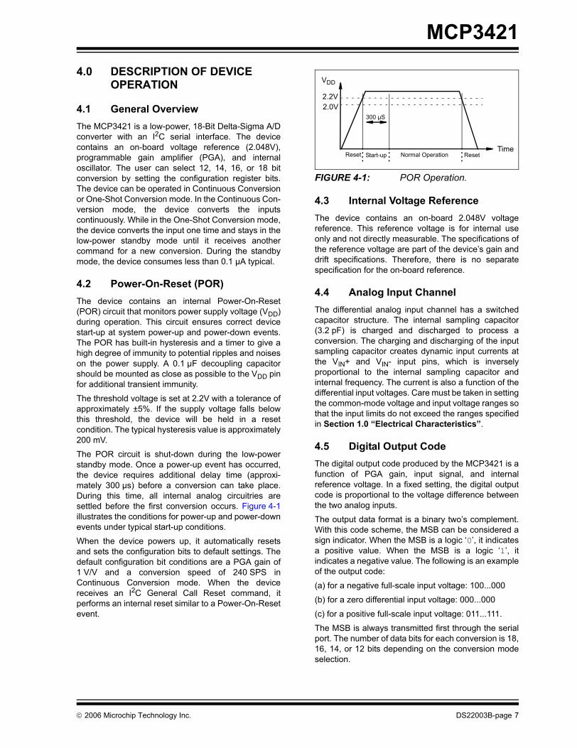
The POR circuit is shut-down during the low-powerstandby mode. Once a power-up event has occurred,the device requires additional delay time (approxi-mately 300 µs) before a conversion can take place.During this time, all internal analog circuitries aresettled before the first conversion occurs. Figure 4-1illustrates the conditions for power-up and power-downevents under typical start-up conditions.
When the device powers up, it automatically resetsand sets the configuration bits to default settings. Thedefault configuration bit conditions are a PGA gain of1 V/V and a conversion speed of 240 SPS inContinuous Conversion mode. When the devicereceives an I2C General Call Reset command, itperforms an internal reset similar to a Power-On-Resetevent.
FIGURE 4-1: POR Operation.
4.3 Internal Voltage Reference The device contains an on-board 2.048V voltagereference. This reference voltage is for internal useonly and not directly measurable. The specifications ofthe reference voltage are part of the device’s gain anddrift specifications. Therefore, there is no separatespecification for the on-board reference.
4.4 Analog Input ChannelThe differential analog input channel has a switchedcapacitor structure. The internal sampling capacitor(3.2 pF) is charged and discharged to process aconversion. The charging and discharging of the inputsampling capacitor creates dynamic input currents atthe VIN+ and VIN- input pins, which is inverselyproportional to the internal sampling capacitor andinternal frequency. The current is also a function of thedifferential input voltages. Care must be taken in settingthe common-mode voltage and input voltage ranges sothat the input limits do not exceed the ranges specifiedin Section 1.0 “Electrical Characteristics”.
4.5 Digital Output CodeThe digital output code produced by the MCP3421 is afunction of PGA gain, input signal, and internalreference voltage. In a fixed setting, the digital outputcode is proportional to the voltage difference betweenthe two analog inputs.
The output data format is a binary two’s complement.With this code scheme, the MSB can be considered asign indicator. When the MSB is a logic ‘0’, it indicatesa positive value. When the MSB is a logic ‘1’, itindicates a negative value. The following is an exampleof the output code:
(a) for a negative full-scale input voltage: 100...000
(b) for a zero differential input voltage: 000...000
(c) for a positive full-scale input voltage: 011...111.
The MSB is always transmitted first through the serialport. The number of data bits for each conversion is 18,16, 14, or 12 bits depending on the conversion modeselection.
VDD
2.2V2.0V
300 µS
Reset Start-up Normal Operation ResetTime
© 2006 Microchip Technology Inc. DS22003B-page 7
MCP3421
The output codes will not roll-over if the input voltageexceeds the maximum input range. In this case, thecode will be locked at 0111...11 for all voltagesgreater than +(VREF - 1 LSB) and 1000...00 forvoltages less than -VREF. Table 4-2 shows an exampleof output codes of various input levels using 18 bitconversion mode. Table 4-3 shows an example ofminimum and maximum codes for each data rateoption.The output code is given by:
EQUATION 4-1:
The LSB of the code is given by:
EQUATION 4-2:
TABLE 4-1: LSB SIZE OF VARIOUS BIT CONVERSION MODES
TABLE 4-2: EXAMPLE OF OUTPUT CODE FOR 18 BITS
TABLE 4-3: MINIMUM AND MAXIMUM CODES
4.6 Self-CalibrationThe device performs a self-calibration of offset andgain for each conversion. This provides reliableconversion results from conversion-to-conversion overvariations in temperature as well as power supplyfluctuations.
4.7 Input ImpedanceThe MCP3421 uses a switched-capacitor input stageusing a 3.2 pF sampling capacitor. This capacitor isswitched (charged and discharged) at a rate of thesampling frequency that is generated by the on-boardclock. The differential mode impedance varies with thePGA settings. The typical differential input impedanceduring a normal mode operation is given by:
Since the sampling capacitor is only switching to theinput pins during a conversion process, the above inputimpedance is only valid during conversion periods. In alow power standby mode, the above impedance is notpresented at the input pins. Therefore, only a leakagecurrent due to ESD diode is presented at the input pins.
The conversion accuracy can be affected by the inputsignal source impedance when any external circuit isconnected to the input pins. The source impedanceadds to the internal impedance and directly affects thetime required to charge the internal sampling capacitor.Therefore, a large input source impedance connectedto the input pins can increase the system performanceerrors such as offset, gain, and integral nonlinearity(INL) errors. Ideally, the input source impedanceshould be zero. This can be achievable by using anoperational amplifier with a closed-loop outputimpedance of tens of ohms.
Bit Resolutions LSB (V)
12 bits 1 mV14 bits 250 µV16 bits 62.5 µV18 bits 15.625 µV
Input Voltage (V) Digital Code
≥ VREF 011111111111111111VREF - 1 LSB 011111111111111111
2 LSB 0000000000000000101 LSB 000000000000000001
0 000000000000000000-1 LSB 111111111111111111-2 LSB 111111111111111110- VREF 100000000000000000
< -VREF 100000000000000000
Output Code Max Code 1+( )VIN+ VIN-–( )
2.048V---------------------------------------×=
LSB 2 2.048V×
2N--------------------------=
Where:
N = the number of bits
Number of Bits Data Rate Minimum
CodeMaximum
Code
12 240 SPS -2048 204714 60 SPS -8192 819116 15 SPS -32768 3276718 3.75 SPS -131072 131071
Note: Maximum n-bit code = 2n-1 - 1Minimum n-bit code = -1 x 2n-1
ZIN(f) = 2.25 MΩ/PGA
DS22003B-page 8 © 2006 Microchip Technology Inc.
MCP3421
4.8 Aliasing and Anti-aliasing FilterAliasing occurs when the input signal contains time-varying signal components with frequency greater thanhalf the sample rate. In the aliasing conditions, thedevice can output unexpected output codes. Forapplications that are operating in electrical noiseenvironments, the time-varying signal noise or highfrequency interference components can be easilyadded to the input signals and cause aliasing. Althoughthe MCP3421 device has an internal first order sincfilter, its’ filter response may not give enoughattenuation to all aliasing signal components. To avoidthe aliasing, an external anti-aliasing filter, which canbe accomplished with a simple RC low-pass filter, istypically used at the input pins. The low-pass filter cutsoff the high frequency noise components and providesa band-limited input signal to the MCP3421 input pins.© 2006 Microchip Technology Inc. DS22003B-page 9
MCP3421
5.0 USING THE MCP3421 DEVICE
5.1 Operating ModesThe user operates the device by setting up the deviceconfiguration register and reads the conversion datausing serial I2C interface commands. The MCP3421operates in two modes: (a) Continuous ConversionMode or (b) One-Shot Conversion Mode (singleconversion). The selection is made by setting the O/Cbit in the Configuration Register. Refer to Section 5.2“Configuration Register” for more information.
5.1.1 CONTINUOUS CONVERSION MODE (O/C BIT = 1)
The MCP3421 device performs a ContinuousConversion if the O/C bit is set to logic “high”. Once theconversion is completed, the result is placed at theoutput data register. The device immediately beginsanother conversion and overwrites the output dataregister with the most recent data.
The device also clears the data ready flag (RDY bit = 0)when the conversion is completed. The device sets theready flag bit (RDY bit = 1), if the latest conversionresult has been read by the Master.
5.1.2 ONE-SHOT CONVERSION MODE (O/C BIT = 0)
Once the One-Shot Conversion (single conversion)Mode is selected, the device performs a conversion,updates the Output Data register, clears the data readyflag (RDY = 0), and then enters a low power standbymode. A new One-Shot Conversion is started againwhen the device receives a new write command withRDY = 1.
This One-Shot Conversion Mode is recommended forlow power operating applications. During the lowcurrent standby mode, the device consumes less than1 µA typical. For example, if user collects 18 bitconversion data once a second in One-Shot Conver-sion mode, the device draws only about one fourth ofits total operating current. In this example, the deviceconsumes approximately 39 µA (= ~145 µA/3.75 SPS),if the device performs only one conversion per second(1 SPS) in 18-bit conversion mode with 3V powersupply.
DS22003B-page 10 © 2006 Microchip Technology Inc.
MCP3421
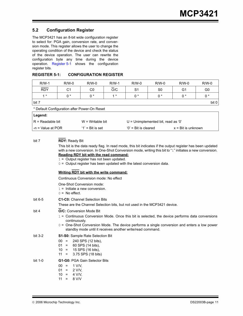
5.2 Configuration RegisterThe MCP3421 has an 8-bit wide configuration registerto select for: PGA gain, conversion rate, and conver-sion mode. This register allows the user to change theoperating condition of the device and check the statusof the device operation. The user can rewrite theconfiguration byte any time during the deviceoperation. Register 5-1 shows the configurationregister bits.REGISTER 5-1: CONFIGURATION REGISTER
R/W-1 R/W-0 R/W-0 R/W-1 R/W-0 R/W-0 R/W-0 R/W-0
RDY C1 C0 O/C S1 S0 G1 G0
1 * 0 * 0 * 1 * 0 * 0 * 0 * 0 *
bit 7 bit 0
* Default Configuration after Power-On Reset
Legend:
R = Readable bit W = Writable bit U = Unimplemented bit, read as ‘0’
-n = Value at POR ‘1’ = Bit is set ‘0’ = Bit is cleared x = Bit is unknown
bit 7 RDY: Ready BitThis bit is the data ready flag. In read mode, this bit indicates if the output register has been updatedwith a new conversion. In One-Shot Conversion mode, writing this bit to “1” initiates a new conversion.Reading RDY bit with the read command:1 = Output register has not been updated.0 = Output register has been updated with the latest conversion data.
Writing RDY bit with the write command:Continuous Conversion mode: No effect
One-Shot Conversion mode:1 = Initiate a new conversion.0 = No effect.
bit 6-5 C1-C0: Channel Selection BitsThese are the Channel Selection bits, but not used in the MCP3421 device.
bit 4 O/C: Conversion Mode Bit1 = Continuous Conversion Mode. Once this bit is selected, the device performs data conversions
continuously.0 = One-Shot Conversion Mode. The device performs a single conversion and enters a low power
standby mode until it receives another write/read command.
bit 3-2 S1-S0: Sample Rate Selection Bit00 = 240 SPS (12 bits), 01 = 60 SPS (14 bits), 10 = 15 SPS (16 bits), 11 = 3.75 SPS (18 bits)
bit 1-0 G1-G0: PGA Gain Selector Bits00 = 1 V/V, 01 = 2 V/V, 10 = 4 V/V, 11 = 8 V/V
© 2006 Microchip Technology Inc. DS22003B-page 11
MCP3421
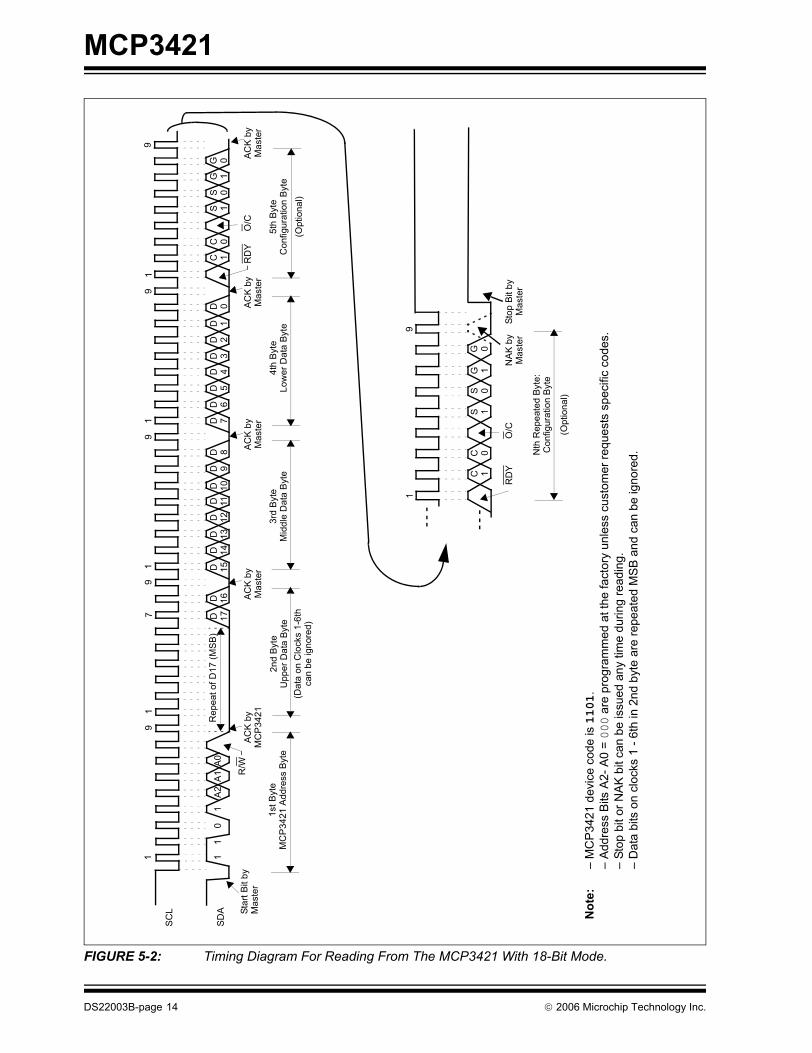
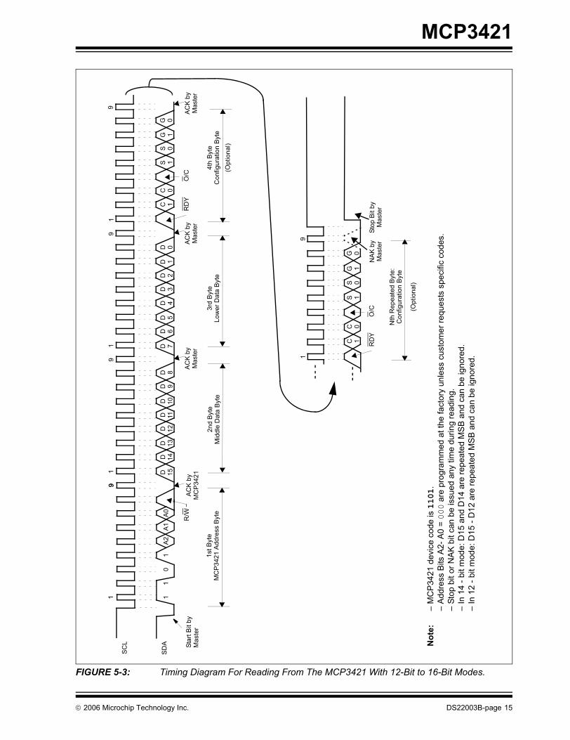
In read mode, the RDY bit in the configuration byteindicates the state of the conversion: (a) RDY = 1indicates that the data bytes that have just been readwere not updated from the previous conversion. (b)RDY = 0 indicates that the data bytes that have justbeen read were updated.If the configuration byte is read repeatedly by clockingcontinuously after the first read (i.e., after the 5th bytein the 18-bit conversion mode), the state of the RDY bitindicates whether the device is ready with newconversion data. See Figure 5-2. For example,RDY = 0 means new conversion data is ready for read-ing. In this case, the user can send a stop bit to exit thecurrent read operation and send a new read commandto read out updated conversion data. See Figures 5-2and 5-3 for reading conversion data. The user canrewrite the configuration byte any time for a newsetting. Tables 5-1 and 5-2 show the examples of theconfiguration bit operation.
5.3 I2C Serial CommunicationsThe MCP3421 device communicates with Master(microcontroller) through a serial I2C (Inter-IntegratedCircuit) interface and supports standard(100 kbits/sec), fast (400 kbits/sec) and high-speed(3.4 Mbits/sec) modes. The serial I2C is a bidirectional2-wire data bus communication protocol using open-drain SCL and SDA lines.
The MCP3421 can only be addressed as a slave. Onceaddressed, it can receive configuration bits or transmitthe latest conversion results. The serial clock pin (SCL)is an input only and the serial data pin (SDA) isbidirectional. An example of a hardware connectiondiagram is shown in Figure 6-1.
The Master starts communication by sending a STARTbit and terminates the communication by sending aSTOP bit. The first byte after the START bit is alwaysthe address byte of the device, which includes thedevice code, the address bits, and the R/W bit. Thedevice code for the MCP3421 device is 1101. Theaddress bits (A2, A1, A0) are pre-programmed at thefactory. In general, the address bits are specified by thecustomer when they order the device. The threeaddress bits are programmed to “000” at the factory, ifthey are not specified by the customer. Figure 5-1shows the details of the MCP3421 address byte.
During a low power standby mode, SDA and SCL pinsremain at a floating condition.
More details of the I2C bus characteristic is describedin Section 5.6 “I2C Bus Characteristics”.
5.3.1 DEVICE ADDRESSINGThe address byte is the first byte received following theSTART condition from the Master device. TheMCP3421 device code is 1101. The device code isfollowed by three address bits (A2, A1, A0) which areprogrammed at the factory. The three address bitsallow up to eight MCP3421 devices on the same databus line. The (R/W) bit determines if the Master devicewants to read the conversion data or write to theConfiguration register. If the (R/W) bit is set (readmode), the MCP3421 outputs the conversion data inthe following clocks. If the (R/W) bit is cleared (writemode), the MCP3421 expects a configuration byte inthe following clocks. When the MCP3421 receives thecorrect address byte, it outputs an acknowledge bitafter the R/W bit. Figure 5-1 shows the MCP3421address byte. See Figures 5-2 and 5-3 for the read andwrite operations of the device.
TABLE 5-1: CONFIGURATION BITS FOR WRITING
R/W O/C RDY Operation0 0 0 No effect if all other bits remain
the same - operation continues with the previous settings
0 0 1 Initiate One-Shot Conversion0 1 0 Initiate Continuous Conversion0 1 1 Initiate Continuous Conversion
TABLE 5-2: CONFIGURATION BITS FOR READING
R/W O/C RDY Operation1 0 0 New conversion data in One-
Shot conversion mode has been just read. The RDY bit remains low until set by a new write command.
1 0 1 One-Shot Conversion is in progress, The conversion data is not updated yet. The RDY bit stays high.
1 1 0 New conversion data in Continu-ous Conversion mode has been just read. The RDY bit changes to high after this read.
1 1 1 The conversion data in Continu-ous Conversion mode was already read. The latest conver-sion data is not ready. The RDY bit stays high until a new conversion is completed.
DS22003B-page 12 © 2006 Microchip Technology Inc.
MCP3421
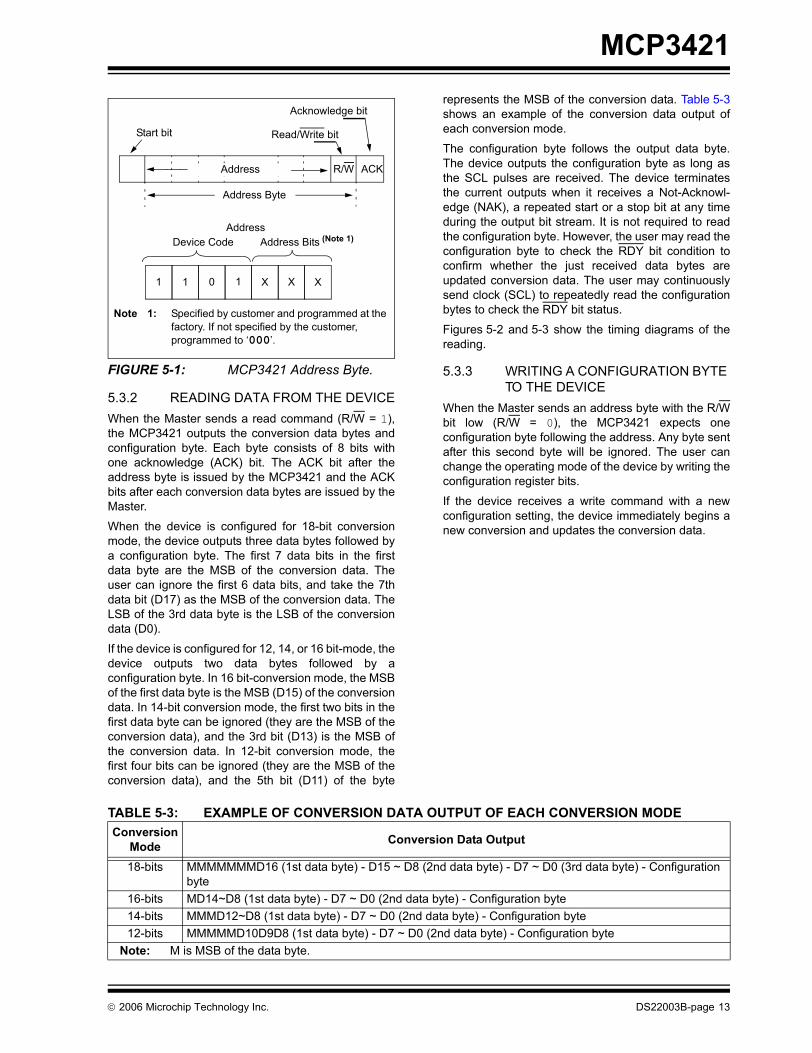
FIGURE 5-1: MCP3421 Address Byte.
5.3.2 READING DATA FROM THE DEVICEWhen the Master sends a read command (R/W = 1),the MCP3421 outputs the conversion data bytes andconfiguration byte. Each byte consists of 8 bits withone acknowledge (ACK) bit. The ACK bit after theaddress byte is issued by the MCP3421 and the ACKbits after each conversion data bytes are issued by theMaster.
When the device is configured for 18-bit conversionmode, the device outputs three data bytes followed bya configuration byte. The first 7 data bits in the firstdata byte are the MSB of the conversion data. Theuser can ignore the first 6 data bits, and take the 7thdata bit (D17) as the MSB of the conversion data. TheLSB of the 3rd data byte is the LSB of the conversiondata (D0).
If the device is configured for 12, 14, or 16 bit-mode, thedevice outputs two data bytes followed by aconfiguration byte. In 16 bit-conversion mode, the MSBof the first data byte is the MSB (D15) of the conversiondata. In 14-bit conversion mode, the first two bits in thefirst data byte can be ignored (they are the MSB of theconversion data), and the 3rd bit (D13) is the MSB ofthe conversion data. In 12-bit conversion mode, thefirst four bits can be ignored (they are the MSB of theconversion data), and the 5th bit (D11) of the byte
represents the MSB of the conversion data. Table 5-3shows an example of the conversion data output ofeach conversion mode.
The configuration byte follows the output data byte.The device outputs the configuration byte as long asthe SCL pulses are received. The device terminatesthe current outputs when it receives a Not-Acknowl-edge (NAK), a repeated start or a stop bit at any timeduring the output bit stream. It is not required to readthe configuration byte. However, the user may read theconfiguration byte to check the RDY bit condition toconfirm whether the just received data bytes areupdated conversion data. The user may continuouslysend clock (SCL) to repeatedly read the configurationbytes to check the RDY bit status.
Figures 5-2 and 5-3 show the timing diagrams of thereading.
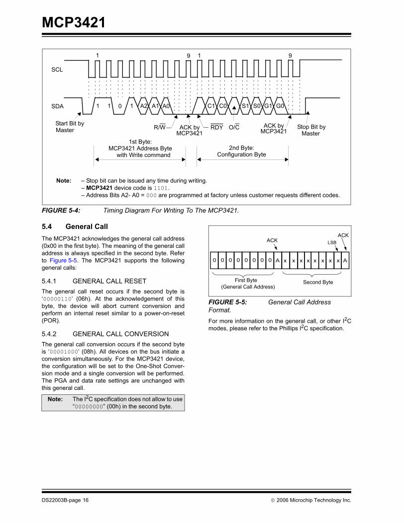
5.3.3 WRITING A CONFIGURATION BYTE TO THE DEVICE
When the Master sends an address byte with the R/Wbit low (R/W = 0), the MCP3421 expects oneconfiguration byte following the address. Any byte sentafter this second byte will be ignored. The user canchange the operating mode of the device by writing theconfiguration register bits.
If the device receives a write command with a newconfiguration setting, the device immediately begins anew conversion and updates the conversion data.
Start bit Read/Write bit
Address Byte
R/W ACK
1 1 0 1 X X X
Device Code Address Bits (Note 1)Address
Acknowledge bit
Address
Note 1: Specified by customer and programmed at the factory. If not specified by the customer, programmed to ‘000’.
TABLE 5-3: EXAMPLE OF CONVERSION DATA OUTPUT OF EACH CONVERSION MODEConversion
Mode Conversion Data Output
18-bits MMMMMMMD16 (1st data byte) - D15 ~ D8 (2nd data byte) - D7 ~ D0 (3rd data byte) - Configuration byte
16-bits MD14~D8 (1st data byte) - D7 ~ D0 (2nd data byte) - Configuration byte14-bits MMMD12~D8 (1st data byte) - D7 ~ D0 (2nd data byte) - Configuration byte12-bits MMMMMD10D9D8 (1st data byte) - D7 ~ D0 (2nd data byte) - Configuration byte
Note: M is MSB of the data byte.
© 2006 Microchip Technology Inc. DS22003B-page 13
MCP3421
FIGURE 5-2: Timing Diagram For Reading From The MCP3421 With 18-Bit Mode.
91
91
91
91
91
91
11
01
A2
A1
A0D
RD
YO
/CAC
K b
yM
CP
3421
7
R/W
Star
t Bit
byM
aste
r
Rep
eat o
f D17
(MSB
)
2nd
Byte
Upp
er D
ata
Byte
(Dat
a on
Clo
cks
1-6t
hca
n be
igno
red)
ACK
by
Mas
ter
ACK
by
Mas
ter
AC
K by
Mas
ter
ACK
byM
aste
r
17D 16
D 15D 14
D 13D 12
D 11D 10
D 9D 8
D 7D 6
D 5D 4
D 3D 2
D 1D 0
C 1C 0
S 1S 0
G 1G 0
1st B
yte
MC
P34
21 A
ddre
ss B
yte
3rd
Byt
eM
iddl
e D
ata
Byt
e4t
h B
yte
Low
er D
ata
Byte
5th
Byt
eC
onfig
urat
ion
Byt
e(O
ptio
nal)
C 1C 0
S 1S 0
G 1G 0
NA
K b
yM
aste
rSt
op B
it by
Mas
ter
(Opt
iona
l)
Nth
Rep
eate
d By
te:
Con
figur
atio
n B
yte
Not
e:–
MC
P342
1 de
vice
cod
e is
1101
.–
Add
ress
Bits
A2-
A0
= 000
are
prog
ram
med
at t
he fa
ctor
y un
less
cus
tom
er re
ques
ts s
peci
fic c
odes
.–
Stop
bit
or N
AK b
it ca
n be
issu
ed a
ny ti
me
durin
g re
adin
g.
– D
ata
bits
on
cloc
ks 1
- 6t
h in
2nd
byt
e ar
e re
peat
ed M
SB a
nd c
an b
e ig
nore
d.
SCL
SDA
RD
YO
/C
DS22003B-page 14 © 2006 Microchip Technology Inc.
MCP3421
FIGURE 5-3: Timing Diagram For Reading From The MCP3421 With 12-Bit to 16-Bit Modes.
11
01
A2A1
A0
AC
K b
yM
CP
3421
Star
t Bit
byM
aste
r
2nd
Byt
eM
iddl
e D
ata
Byt
e
AC
K by
Mas
ter
ACK
by
Mas
ter
AC
K b
yM
aste
r
D 15D 14
D 13D 12
D 11D 10
D 9D 8
D 7D 6
D 5D 4
D 3D 2
D 1D 0
C 1C 0
S 1S 0
G 1G 0
1st B
yte
MC
P34
21 A
ddre
ss B
yte
3rd
Byt
eLo
wer
Dat
a B
yte
4th
Byte
Con
figur
atio
n B
yte
(Opt
iona
l)
C 1C 0
S 1S 0
G 1G 0
NA
K b
yM
aste
rSt
op B
it by
Mas
ter
(Opt
iona
l)
Nth
Rep
eate
d By
te:
Con
figur
atio
n B
yte
Not
e:–
MC
P342
1 de
vice
cod
e is
1101
.–
Add
ress
Bits
A2-
A0
= 000
are
prog
ram
med
at t
he fa
ctor
y un
less
cus
tom
er re
ques
ts s
peci
fic c
odes
.–
Stop
bit
or N
AK
bit c
an b
e is
sued
any
tim
e du
ring
read
ing.
–
In 1
4 - b
it m
ode:
D15
and
D14
are
repe
ated
MSB
and
can
be
igno
red.
– In
12
- bit
mod
e: D
15 -
D12
are
repe
ated
MSB
and
can
be
igno
red.
91
99
19
19
1
SC
L
SD
A
91
RD
YO
/CR
/W
RD
YO
/C
© 2006 Microchip Technology Inc. DS22003B-page 15
MCP3421
FIGURE 5-4: Timing Diagram For Writing To The MCP3421.
5.4 General CallThe MCP3421 acknowledges the general call address(0x00 in the first byte). The meaning of the general calladdress is always specified in the second byte. Referto Figure 5-5. The MCP3421 supports the followinggeneral calls:
5.4.1 GENERAL CALL RESETThe general call reset occurs if the second byte is‘00000110’ (06h). At the acknowledgement of thisbyte, the device will abort current conversion andperform an internal reset similar to a power-on-reset(POR).
5.4.2 GENERAL CALL CONVERSIONThe general call conversion occurs if the second byteis ‘00001000’ (08h). All devices on the bus initiate aconversion simultaneously. For the MCP3421 device,the configuration will be set to the One-Shot Conver-sion mode and a single conversion will be performed.The PGA and data rate settings are unchanged withthis general call.
FIGURE 5-5: General Call Address Format.For more information on the general call, or other I2Cmodes, please refer to the Phillips I2C specification.
91 91
Stop Bit by
1 1 0 1 A2 A1 A0
R/W ACK byMCP3421
RDY
C1 C0
O/C
S1 S0 G1 G0
1st Byte:2nd Byte:
Master ACK by
MCP3421
MCP3421 Address Byte Configuration Byte
Start Bit byMaster
with Write command
Note: – Stop bit can be issued any time during writing. – MCP3421 device code is 1101.– Address Bits A2- A0 = 000 are programmed at factory unless customer requests different codes.
SCL
SDA
Note: The I2C specification does not allow to use“00000000” (00h) in the second byte.
LSB
First Byte
ACK
x0 0 0 0 0 0 0 0 A Ax x x x x x x
(General Call Address)Second Byte
ACK
DS22003B-page 16 © 2006 Microchip Technology Inc.
MCP3421
5.5 High-Speed (HS) ModeThe I2C specification requires that a high-speed modedevice must be ‘activated’ to operate in high-speedmode. This is done by sending a special address byteof 00001XXX following the START bit. The XXX bits areunique to the High-Speed (HS) mode Master. This byteis referred to as the High-Speed (HS) Master ModeCode (HSMMC). The MCP3421 device does notacknowledge this byte. However, upon receiving thiscode, the MCP3421 switches on its HS mode filtersand communicates up to 3.4 MHz on SDA and SCL.The device will switch out of the HS mode on the nextSTOP condition.For more information on the HS mode, or other I2Cmodes, please refer to the Phillips I2C specification.
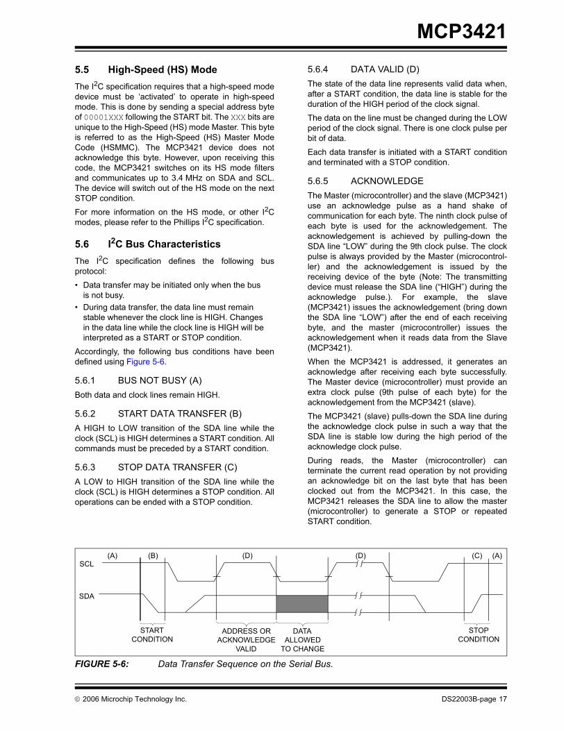
5.6 I2C Bus CharacteristicsThe I2C specification defines the following busprotocol:
• Data transfer may be initiated only when the bus is not busy.
• During data transfer, the data line must remain stable whenever the clock line is HIGH. Changes in the data line while the clock line is HIGH will be interpreted as a START or STOP condition.
Accordingly, the following bus conditions have beendefined using Figure 5-6.
5.6.1 BUS NOT BUSY (A)Both data and clock lines remain HIGH.
5.6.2 START DATA TRANSFER (B)A HIGH to LOW transition of the SDA line while theclock (SCL) is HIGH determines a START condition. Allcommands must be preceded by a START condition.
5.6.3 STOP DATA TRANSFER (C)A LOW to HIGH transition of the SDA line while theclock (SCL) is HIGH determines a STOP condition. Alloperations can be ended with a STOP condition.
5.6.4 DATA VALID (D)The state of the data line represents valid data when,after a START condition, the data line is stable for theduration of the HIGH period of the clock signal.
The data on the line must be changed during the LOWperiod of the clock signal. There is one clock pulse perbit of data.
Each data transfer is initiated with a START conditionand terminated with a STOP condition.
5.6.5 ACKNOWLEDGEThe Master (microcontroller) and the slave (MCP3421)use an acknowledge pulse as a hand shake ofcommunication for each byte. The ninth clock pulse ofeach byte is used for the acknowledgement. Theacknowledgement is achieved by pulling-down theSDA line “LOW” during the 9th clock pulse. The clockpulse is always provided by the Master (microcontrol-ler) and the acknowledgement is issued by thereceiving device of the byte (Note: The transmittingdevice must release the SDA line (“HIGH”) during theacknowledge pulse.). For example, the slave(MCP3421) issues the acknowledgement (bring downthe SDA line “LOW”) after the end of each receivingbyte, and the master (microcontroller) issues theacknowledgement when it reads data from the Slave(MCP3421).
When the MCP3421 is addressed, it generates anacknowledge after receiving each byte successfully.The Master device (microcontroller) must provide anextra clock pulse (9th pulse of each byte) for theacknowledgement from the MCP3421 (slave).
The MCP3421 (slave) pulls-down the SDA line duringthe acknowledge clock pulse in such a way that theSDA line is stable low during the high period of theacknowledge clock pulse.
During reads, the Master (microcontroller) canterminate the current read operation by not providingan acknowledge bit on the last byte that has beenclocked out from the MCP3421. In this case, theMCP3421 releases the SDA line to allow the master(microcontroller) to generate a STOP or repeatedSTART condition.
FIGURE 5-6: Data Transfer Sequence on the Serial Bus.
SCL
SDA
(A) (B) (D) (D) (A)(C)
STARTCONDITION
ADDRESS ORACKNOWLEDGE
VALID
DATAALLOWED
TO CHANGE
STOPCONDITION
© 2006 Microchip Technology Inc. DS22003B-page 17
MCP3421
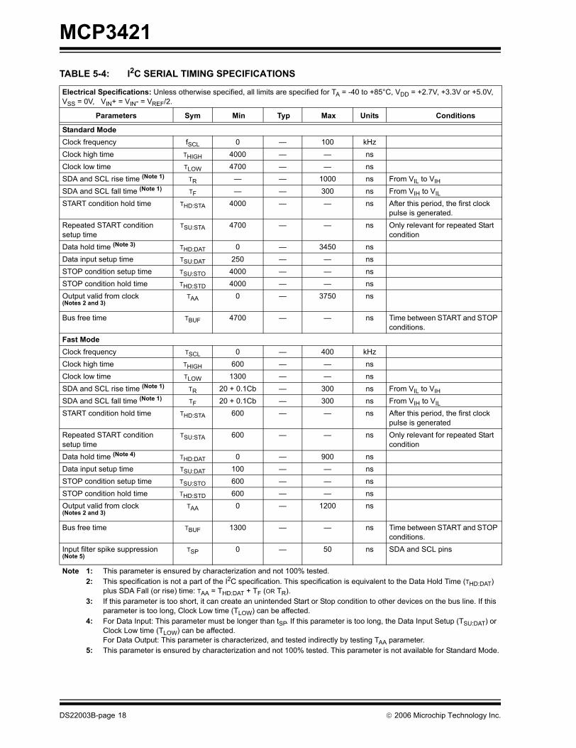
TABLE 5-4: I2C SERIAL TIMING SPECIFICATIONS
Electrical Specifications: Unless otherwise specified, all limits are specified for TA = -40 to +85°C, VDD = +2.7V, +3.3V or +5.0V, VSS = 0V, VIN+ = VIN- = VREF/2.
Parameters Sym Min Typ Max Units Conditions
Standard ModeClock frequency fSCL 0 — 100 kHzClock high time THIGH 4000 — — nsClock low time TLOW 4700 — — nsSDA and SCL rise time (Note 1) TR — — 1000 ns From VIL to VIH
SDA and SCL fall time (Note 1) TF — — 300 ns From VIH to VIL
START condition hold time THD:STA 4000 — — ns After this period, the first clock pulse is generated.
Repeated START condition setup time
TSU:STA 4700 — — ns Only relevant for repeated Start condition
Data hold time (Note 3) THD:DAT 0 — 3450 nsData input setup time TSU:DAT 250 — — nsSTOP condition setup time TSU:STO 4000 — — nsSTOP condition hold time THD:STD 4000 — — nsOutput valid from clock(Notes 2 and 3)
TAA 0 — 3750 ns
Bus free time TBUF 4700 — — ns Time between START and STOP conditions.
Fast ModeClock frequency TSCL 0 — 400 kHzClock high time THIGH 600 — — nsClock low time TLOW 1300 — — nsSDA and SCL rise time (Note 1) TR 20 + 0.1Cb — 300 ns From VIL to VIH
SDA and SCL fall time (Note 1) TF 20 + 0.1Cb — 300 ns From VIH to VIL
START condition hold time THD:STA 600 — — ns After this period, the first clock pulse is generated
Repeated START condition setup time
TSU:STA 600 — — ns Only relevant for repeated Start condition
Data hold time (Note 4) THD:DAT 0 — 900 nsData input setup time TSU:DAT 100 — — nsSTOP condition setup time TSU:STO 600 — — nsSTOP condition hold time THD:STD 600 — — nsOutput valid from clock(Notes 2 and 3)
TAA 0 — 1200 ns
Bus free time TBUF 1300 — — ns Time between START and STOP conditions.
Input filter spike suppression(Note 5)
TSP 0 — 50 ns SDA and SCL pins
Note 1: This parameter is ensured by characterization and not 100% tested.2: This specification is not a part of the I2C specification. This specification is equivalent to the Data Hold Time (THD:DAT)
plus SDA Fall (or rise) time: TAA = THD:DAT + TF (OR TR).3: If this parameter is too short, it can create an unintended Start or Stop condition to other devices on the bus line. If this
parameter is too long, Clock Low time (TLOW) can be affected. 4: For Data Input: This parameter must be longer than tSP. If this parameter is too long, the Data Input Setup (TSU:DAT) or
Clock Low time (TLOW) can be affected.For Data Output: This parameter is characterized, and tested indirectly by testing TAA parameter.
5: This parameter is ensured by characterization and not 100% tested. This parameter is not available for Standard Mode.
DS22003B-page 18 © 2006 Microchip Technology Inc.
MCP3421
High Speed ModeClock frequency fSCL 0 — 3.4
1.7MHzMHz
Cb = 100 pFCb = 400 pF
Clock high time THIGH 60120
— — nsns
Cb = 100 pFCb = 400 pF
Clock low time TLOW 160320
— — ns Cb = 100 pFCb = 400 pF
SCL rise time (Note 1) TR — — 4080
ns From VIL to VIH,Cb = 100 pFCb = 400 pF
SCL fall time (Note 1) TF — — 4080
ns From VIH to VIL,Cb = 100 pFCb = 400 pF
SDA rise time (Note 1) TR: DAT — — 80160
ns From VIL to VIH,Cb = 100 pFCb = 400 pF
SDA fall time (Note 1) TF: DATA — — 80160
ns From VIH to VIL,Cb = 100 pFCb = 400 pF
START condition hold time THD:STA 160 — — ns After this period, the first clock pulse is generated
Repeated START condition setup time
TSU:STA 160 — — ns Only relevant for repeated Start condition
Data hold time (Note 4) THD:DAT 00
— 70150
ns Cb = 100 pFCb = 400 pF
Data input setup time TSU:DAT 10 — — nsSTOP condition setup time TSU:STO 160 — — nsSTOP condition hold time THD:STD 160 — — nsOutput valid from clock(Notes 2 and 3)
TAA — — 150310
ns Cb = 100 pFCb = 400 pF
Bus free time TBUF 160 — — ns Time between START and STOP conditions.
Input filter spike suppression (Note 5)
TSP 0 — 10 ns SDA and SCL pins
TABLE 5-4: I2C SERIAL TIMING SPECIFICATIONS (CONTINUED)
Electrical Specifications: Unless otherwise specified, all limits are specified for TA = -40 to +85°C, VDD = +2.7V, +3.3V or +5.0V, VSS = 0V, VIN+ = VIN- = VREF/2.
Parameters Sym Min Typ Max Units Conditions
Note 1: This parameter is ensured by characterization and not 100% tested.2: This specification is not a part of the I2C specification. This specification is equivalent to the Data Hold Time (THD:DAT)
plus SDA Fall (or rise) time: TAA = THD:DAT + TF (OR TR).3: If this parameter is too short, it can create an unintended Start or Stop condition to other devices on the bus line. If this
parameter is too long, Clock Low time (TLOW) can be affected. 4: For Data Input: This parameter must be longer than tSP. If this parameter is too long, the Data Input Setup (TSU:DAT) or
Clock Low time (TLOW) can be affected.For Data Output: This parameter is characterized, and tested indirectly by testing TAA parameter.
5: This parameter is ensured by characterization and not 100% tested. This parameter is not available for Standard Mode.
© 2006 Microchip Technology Inc. DS22003B-page 19
MCP3421
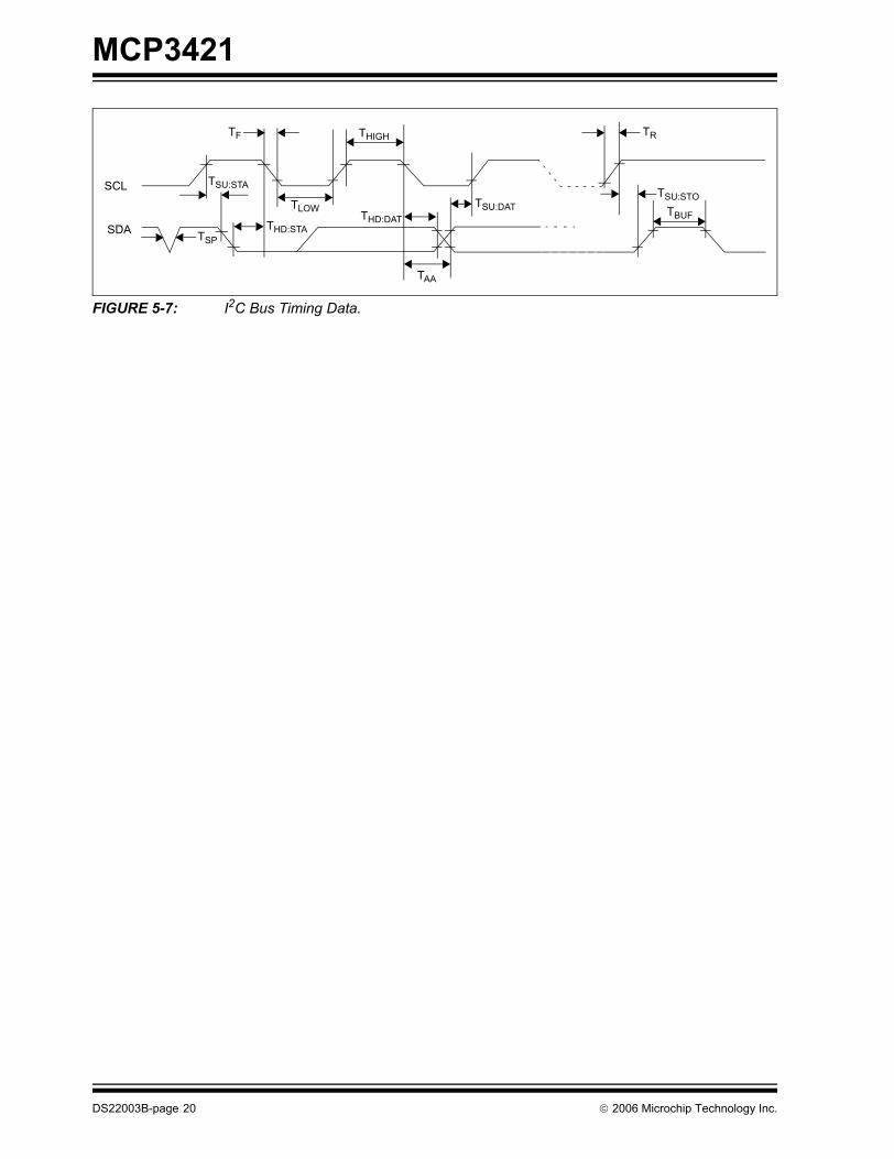
FIGURE 5-7: I2C Bus Timing Data.
TF
SCL
SDA
TSU:STA
TSPTHD:STA
TLOW
THIGH
THD:DAT
TAA
TSU:DAT
TR
TSU:STO
TBUF
DS22003B-page 20 © 2006 Microchip Technology Inc.
MCP3421
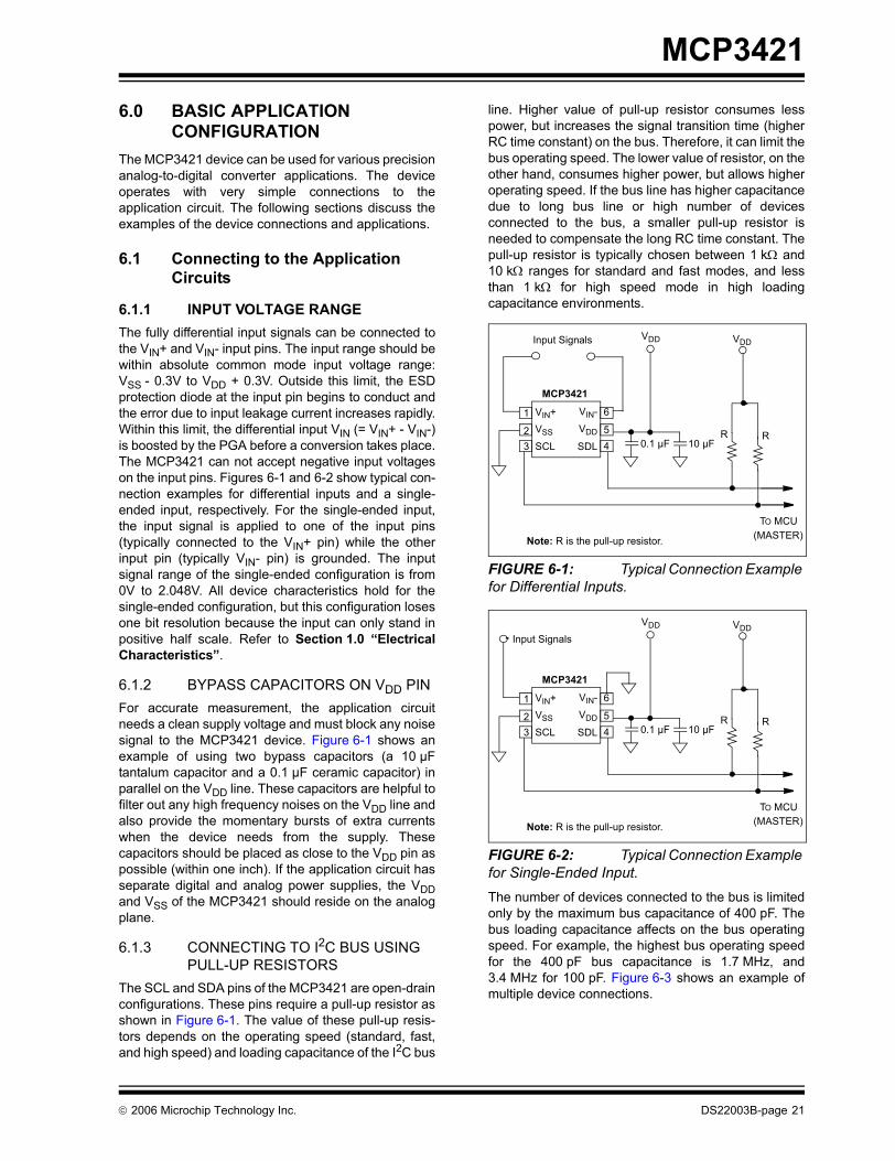
6.0 BASIC APPLICATION CONFIGURATION
The MCP3421 device can be used for various precisionanalog-to-digital converter applications. The deviceoperates with very simple connections to theapplication circuit. The following sections discuss theexamples of the device connections and applications.
6.1 Connecting to the Application Circuits
6.1.1 INPUT VOLTAGE RANGEThe fully differential input signals can be connected tothe VIN+ and VIN- input pins. The input range should bewithin absolute common mode input voltage range:VSS - 0.3V to VDD + 0.3V. Outside this limit, the ESDprotection diode at the input pin begins to conduct andthe error due to input leakage current increases rapidly.Within this limit, the differential input VIN (= VIN+ - VIN-)is boosted by the PGA before a conversion takes place.The MCP3421 can not accept negative input voltageson the input pins. Figures 6-1 and 6-2 show typical con-nection examples for differential inputs and a single-ended input, respectively. For the single-ended input,the input signal is applied to one of the input pins(typically connected to the VIN+ pin) while the otherinput pin (typically VIN- pin) is grounded. The inputsignal range of the single-ended configuration is from0V to 2.048V. All device characteristics hold for thesingle-ended configuration, but this configuration losesone bit resolution because the input can only stand inpositive half scale. Refer to Section 1.0 “ElectricalCharacteristics”.
6.1.2 BYPASS CAPACITORS ON VDD PINFor accurate measurement, the application circuitneeds a clean supply voltage and must block any noisesignal to the MCP3421 device. Figure 6-1 shows anexample of using two bypass capacitors (a 10 µFtantalum capacitor and a 0.1 µF ceramic capacitor) inparallel on the VDD line. These capacitors are helpful tofilter out any high frequency noises on the VDD line andalso provide the momentary bursts of extra currentswhen the device needs from the supply. Thesecapacitors should be placed as close to the VDD pin aspossible (within one inch). If the application circuit hasseparate digital and analog power supplies, the VDDand VSS of the MCP3421 should reside on the analogplane.
6.1.3 CONNECTING TO I2C BUS USING PULL-UP RESISTORS
The SCL and SDA pins of the MCP3421 are open-drainconfigurations. These pins require a pull-up resistor asshown in Figure 6-1. The value of these pull-up resis-tors depends on the operating speed (standard, fast,and high speed) and loading capacitance of the I2C bus
line. Higher value of pull-up resistor consumes lesspower, but increases the signal transition time (higherRC time constant) on the bus. Therefore, it can limit thebus operating speed. The lower value of resistor, on theother hand, consumes higher power, but allows higheroperating speed. If the bus line has higher capacitancedue to long bus line or high number of devicesconnected to the bus, a smaller pull-up resistor isneeded to compensate the long RC time constant. Thepull-up resistor is typically chosen between 1 kΩ and10 kΩ ranges for standard and fast modes, and lessthan 1 kΩ for high speed mode in high loadingcapacitance environments.
FIGURE 6-1: Typical Connection Example for Differential Inputs.
FIGURE 6-2: Typical Connection Example for Single-Ended Input.The number of devices connected to the bus is limitedonly by the maximum bus capacitance of 400 pF. Thebus loading capacitance affects on the bus operatingspeed. For example, the highest bus operating speedfor the 400 pF bus capacitance is 1.7 MHz, and3.4 MHz for 100 pF. Figure 6-3 shows an example ofmultiple device connections.
MCP3421
VIN+ VIN-
VDDVSS
1
23 4
5
6
SCL SDL 10 µF0.1 µFR R
Input Signals VDD VDD
TO MCU(MASTER)Note: R is the pull-up resistor.
MCP3421
VIN+ VIN-
VDDVSS
1
23 4
5
6
SCL SDL 10 µF0.1 µFR R
Input Signals
VDD VDD
TO MCU(MASTER)Note: R is the pull-up resistor.
© 2006 Microchip Technology Inc. DS22003B-page 21
MCP3421
FIGURE 6-3: Example of Multiple Device Connection on I2C Bus.
6.2 Device Connection TestThe user can test the presence of the MCP3421 on theI2C bus line without performing an input data conver-sion. This test can be achieved by checking anacknowledge response from the MCP3421 after send-ing a read or write command. Here is an example usingFigure 6-4:
(a) Set the R/W bit “HIGH” in the address byte.
(b) The MCP3421 will then acknowledge by pullingSDA bus LOW during the ACK clock and then releasethe bus back to the I2C Master.
(c) A STOP or repeated START bit can then be issuedfrom the Master and I2C communication can continue.
FIGURE 6-4: I2C Bus Connection Test.
6.3 Application ExamplesThe MCP3421 device can be used in a broad range ofsensor and data acquisition applications. Figure 6-5,shows an example of interfacing with a bridge sensorfor pressure measurement.
FIGURE 6-5: Example of Pressure Measurement.In this circuit example, the sensor full scale range is±7.5 mV with a common mode input voltage of VDD / 2.This configuration will provide a full 14-bit resolutionacross the sensor output range. The alternative circuitfor this amount of accuracy would involve an analoggain stage prior to a 16-bit ADC.
Figure 6-6 shows an example of temperature measure-ment using a thermistor. This example can achieve alinear response over a 50°C temperature range. Thiscan be implemented using a standard resistor with 1%tolerance in series with the thermistor. The value of theresistor is selected to be equal to the thermistor valueat the mid-point of the desired temperature range.
FIGURE 6-6: Example of Temperature Measurement.
SDA SCL
(24LC01)
Microcontroller
EEPROM
MCP3421
(TC74)
TemperatureSensor
(PIC16F876)
1 2 3 4 5 6 7 8 9SCL
SDA 1 1 0 1 A2 A1 A0 1
StartBit
Address Byte
Address bits Device bits R/W
StartBit
MCP3421
AC
K
Response
NPP301
MCP3421
VIN+ VIN-
VDDVSS
1
23 4
5
6
SCL SDL 10 µF0.1 µFR R
VDD VDD
TO MCU(MASTER)
VDD
10 kΩResistor
10 kΩThermistor
MCP3421
VIN+ VIN-
VDDVSS
1
23 4
5
6
SCL SDL 10 µF0.1 µFR R
VDD VDD
TO MCU(MASTER)
VDD
DS22003B-page 22 © 2006 Microchip Technology Inc.
MCP3421
7.0 PACKAGING INFORMATION
7.1 Package Marking Information
Legend: XX...X Customer-specific informationY Year code (last digit of calendar year)YY Year code (last 2 digits of calendar year)WW Week code (week of January 1 is week ‘01’)NNN Alphanumeric traceability code Pb-free JEDEC designator for Matte Tin (Sn)* This package is Pb-free. The Pb-free JEDEC designator ( )
can be found on the outer packaging for this package.
Note: In the event the full Microchip part number cannot be marked on one line, it willbe carried over to the next line, thus limiting the number of availablecharacters for customer-specific information.
3e
3e
25
13
64
6-Lead SOT-23
XXNN 25
13
64
Example
CA25
© 2006 Microchip Technology Inc. DS22003B-page 23
MCP3421
6-Lead Plastic Small Outline Transistor (OT) (SOT-23)Note: For the most current package drawings, please see the Microchip Packaging Specification located at http://www.microchip.com/packaging
1
DB
n
E
E1
L
c
β
φ
α
A2A
A1
p1
10501050βMold Draft Angle Bottom10501050αMold Draft Angle Top
0.500.430.35.020.017.014BLead Width0.200.150.09.008.006.004cLead Thickness
10501050φFoot Angle0.550.450.35.022.018.014LFoot Length3.102.952.80.122.116.110DOverall Length1.751.631.50.069.064.059E1Molded Package Width3.002.802.60.118.110.102EOverall Width0.150.080.00.006.003.000A1Standoff1.301.100.90.051.043.035A2Molded Package Thickness1.451.180.90.057.046.035AOverall Height
1.90 BSC.075 BSCp1Outside lead pitch0.95 BSC.038 BSCpPitch
66nNumber of PinsMAXNOMMINMAXNOMMINDimension Limits
MILLIMETERSINCHES*Units
Dimensions D and E1 do not include mold flash or protrusions. Mold flash or protrusions shall not exceed .005" (0.127mm) per side.Notes:
JEITA (formerly EIAJ) equivalent: SC-74A
* Controlling Parameter
Drawing No. C04-120
BSC: Basic Dimension. Theoretically exact value shown without tolerances. See ASME Y14.5M
Revised 09-12-05
DS22003B-page 24 © 2006 Microchip Technology Inc.
MCP3421
APPENDIX A: REVISION HISTORY
Revision B (December 2006)• Changes to Electrical Characteristics tables• Added characterization data• Changes to I2C Serial Timing Specification table• Change to Figure 5-7.
Revision A (August 2006)• Original Release of this Document.
© 2006 Microchip Technology Inc. DS22003B-page 27

MCP3421
NOTES:DS22003B-page 28 © 2006 Microchip Technology Inc.
MCP3421
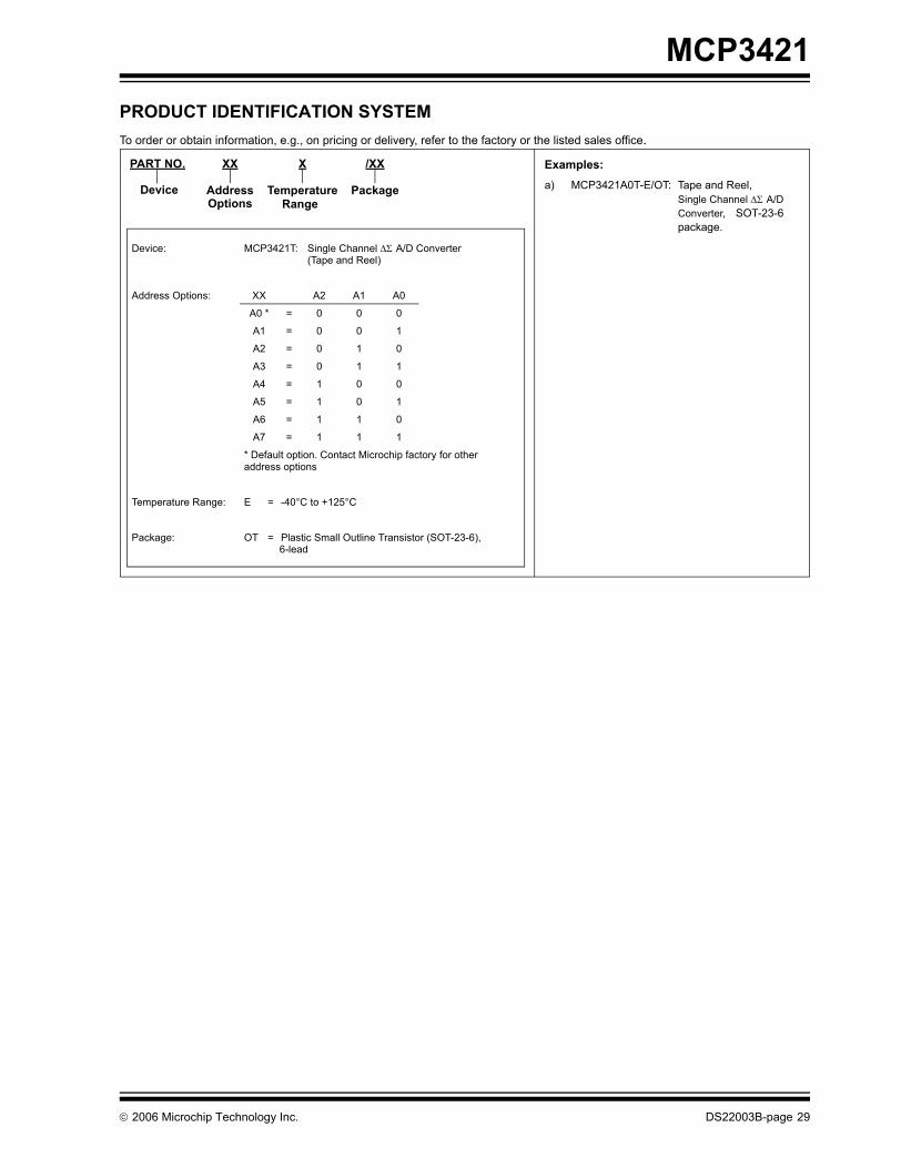
PRODUCT IDENTIFICATION SYSTEMTo order or obtain information, e.g., on pricing or delivery, refer to the factory or the listed sales office.
Device: MCP3421T: Single Channel ΔΣ A/D Converter
(Tape and Reel)
Address Options: XX A2 A1 A0
A0 * = 0 0 0
A1 = 0 0 1
A2 = 0 1 0
A3 = 0 1 1
A4 = 1 0 0
A5 = 1 0 1
A6 = 1 1 0
A7 = 1 1 1
* Default option. Contact Microchip factory for other address options
Temperature Range: E = -40°C to +125°C
Package: OT = Plastic Small Outline Transistor (SOT-23-6),6-lead
Examples:a) MCP3421A0T-E/OT: Tape and Reel,
Single Channel ΔΣ A/DConverter, SOT-23-6package.
PART NO. XXX
Address TemperatureRange
Device
/XX
PackageOptions
© 2006 Microchip Technology Inc. DS22003B-page 29
MCP3421
NOTES:DS22003B-page 30 © 2006 Microchip Technology Inc.
Note the following details of the code protection feature on Microchip devices:• Microchip products meet the specification contained in their particular Microchip Data Sheet.
• Microchip believes that its family of products is one of the most secure families of its kind on the market today, when used in the intended manner and under normal conditions.
• There are dishonest and possibly illegal methods used to breach the code protection feature. All of these methods, to our knowledge, require using the Microchip products in a manner outside the operating specifications contained in Microchip’s Data Sheets. Most likely, the person doing so is engaged in theft of intellectual property.
• Microchip is willing to work with the customer who is concerned about the integrity of their code.
• Neither Microchip nor any other semiconductor manufacturer can guarantee the security of their code. Code protection does not mean that we are guaranteeing the product as “unbreakable.”
Code protection is constantly evolving. We at Microchip are committed to continuously improving the code protection features of ourproducts. Attempts to break Microchip’s code protection feature may be a violation of the Digital Millennium Copyright Act. If such actsallow unauthorized access to your software or other copyrighted work, you may have a right to sue for relief under that Act.
Information contained in this publication regarding deviceapplications and the like is provided only for your convenienceand may be superseded by updates. It is your responsibility toensure that your application meets with your specifications.MICROCHIP MAKES NO REPRESENTATIONS ORWARRANTIES OF ANY KIND WHETHER EXPRESS ORIMPLIED, WRITTEN OR ORAL, STATUTORY OROTHERWISE, RELATED TO THE INFORMATION,INCLUDING BUT NOT LIMITED TO ITS CONDITION,QUALITY, PERFORMANCE, MERCHANTABILITY ORFITNESS FOR PURPOSE. Microchip disclaims all liabilityarising from this information and its use. Use of Microchipdevices in life support and/or safety applications is entirely atthe buyer’s risk, and the buyer agrees to defend, indemnify andhold harmless Microchip from any and all damages, claims,suits, or expenses resulting from such use. No licenses areconveyed, implicitly or otherwise, under any Microchipintellectual property rights.
© 2006 Microchip Technology Inc.
Trademarks
The Microchip name and logo, the Microchip logo, Accuron, dsPIC, KEELOQ, microID, MPLAB, PIC, PICmicro, PICSTART, PRO MATE, PowerSmart, rfPIC, and SmartShunt are registered trademarks of Microchip Technology Incorporated in the U.S.A. and other countries.
AmpLab, FilterLab, Migratable Memory, MXDEV, MXLAB, SEEVAL, SmartSensor and The Embedded Control Solutions Company are registered trademarks of Microchip Technology Incorporated in the U.S.A.
Analog-for-the-Digital Age, Application Maestro, CodeGuard, dsPICDEM, dsPICDEM.net, dsPICworks, ECAN, ECONOMONITOR, FanSense, FlexROM, fuzzyLAB, In-Circuit Serial Programming, ICSP, ICEPIC, Linear Active Thermistor, Mindi, MiWi, MPASM, MPLIB, MPLINK, PICkit, PICDEM, PICDEM.net, PICLAB, PICtail, PowerCal, PowerInfo, PowerMate, PowerTool, REAL ICE, rfLAB, rfPICDEM, Select Mode, Smart Serial, SmartTel, Total Endurance, UNI/O, WiperLock and ZENA are trademarks of Microchip Technology Incorporated in the U.S.A. and other countries.
SQTP is a service mark of Microchip Technology Incorporated in the U.S.A.
All other trademarks mentioned herein are property of their respective companies.
© 2006, Microchip Technology Incorporated, Printed in the U.S.A., All Rights Reserved.
Printed on recycled paper.
DS22003B-page 31
Microchip received ISO/TS-16949:2002 certification for its worldwide headquarters, design and wafer fabrication facilities in Chandler and Tempe, Arizona, Gresham, Oregon and Mountain View, California. The Company’s quality system processes and procedures are for its PIC®
8-bit MCUs, KEELOQ® code hopping devices, Serial EEPROMs, microperipherals, nonvolatile memory and analog products. In addition, Microchip’s quality system for the design and manufacture of development systems is ISO 9001:2000 certified.

DS22003B-page 32 © 2006 Microchip Technology Inc.
AMERICASCorporate Office2355 West Chandler Blvd.Chandler, AZ 85224-6199Tel: 480-792-7200 Fax: 480-792-7277Technical Support: http://support.microchip.comWeb Address: www.microchip.comAtlantaAlpharetta, GA Tel: 770-640-0034 Fax: 770-640-0307BostonWestborough, MA Tel: 774-760-0087 Fax: 774-760-0088ChicagoItasca, IL Tel: 630-285-0071 Fax: 630-285-0075DallasAddison, TX Tel: 972-818-7423 Fax: 972-818-2924DetroitFarmington Hills, MI Tel: 248-538-2250Fax: 248-538-2260KokomoKokomo, IN Tel: 765-864-8360Fax: 765-864-8387Los AngelesMission Viejo, CA Tel: 949-462-9523 Fax: 949-462-9608Santa ClaraSanta Clara, CA Tel: 408-961-6444Fax: 408-961-6445TorontoMississauga, Ontario, CanadaTel: 905-673-0699 Fax: 905-673-6509
ASIA/PACIFICAsia Pacific OfficeSuites 3707-14, 37th FloorTower 6, The GatewayHabour City, KowloonHong KongTel: 852-2401-1200Fax: 852-2401-3431Australia - SydneyTel: 61-2-9868-6733Fax: 61-2-9868-6755China - BeijingTel: 86-10-8528-2100 Fax: 86-10-8528-2104China - ChengduTel: 86-28-8665-5511Fax: 86-28-8665-7889China - FuzhouTel: 86-591-8750-3506 Fax: 86-591-8750-3521China - Hong Kong SARTel: 852-2401-1200 Fax: 852-2401-3431China - QingdaoTel: 86-532-8502-7355Fax: 86-532-8502-7205China - ShanghaiTel: 86-21-5407-5533 Fax: 86-21-5407-5066China - ShenyangTel: 86-24-2334-2829Fax: 86-24-2334-2393China - ShenzhenTel: 86-755-8203-2660 Fax: 86-755-8203-1760China - ShundeTel: 86-757-2839-5507 Fax: 86-757-2839-5571China - WuhanTel: 86-27-5980-5300Fax: 86-27-5980-5118China - XianTel: 86-29-8833-7250Fax: 86-29-8833-7256
ASIA/PACIFICIndia - BangaloreTel: 91-80-4182-8400 Fax: 91-80-4182-8422India - New DelhiTel: 91-11-4160-8631Fax: 91-11-4160-8632India - PuneTel: 91-20-2566-1512Fax: 91-20-2566-1513Japan - YokohamaTel: 81-45-471- 6166 Fax: 81-45-471-6122Korea - GumiTel: 82-54-473-4301Fax: 82-54-473-4302Korea - SeoulTel: 82-2-554-7200Fax: 82-2-558-5932 or 82-2-558-5934Malaysia - PenangTel: 60-4-646-8870Fax: 60-4-646-5086Philippines - ManilaTel: 63-2-634-9065Fax: 63-2-634-9069SingaporeTel: 65-6334-8870Fax: 65-6334-8850Taiwan - Hsin ChuTel: 886-3-572-9526Fax: 886-3-572-6459Taiwan - KaohsiungTel: 886-7-536-4818Fax: 886-7-536-4803Taiwan - TaipeiTel: 886-2-2500-6610 Fax: 886-2-2508-0102Thailand - BangkokTel: 66-2-694-1351Fax: 66-2-694-1350
EUROPEAustria - WelsTel: 43-7242-2244-39Fax: 43-7242-2244-393Denmark - CopenhagenTel: 45-4450-2828 Fax: 45-4485-2829France - ParisTel: 33-1-69-53-63-20 Fax: 33-1-69-30-90-79Germany - MunichTel: 49-89-627-144-0 Fax: 49-89-627-144-44Italy - Milan Tel: 39-0331-742611 Fax: 39-0331-466781Netherlands - DrunenTel: 31-416-690399 Fax: 31-416-690340Spain - MadridTel: 34-91-708-08-90Fax: 34-91-708-08-91UK - WokinghamTel: 44-118-921-5869Fax: 44-118-921-5820
WORLDWIDE SALES AND SERVICE
10/19/06


![maredu.gunet.gr · Web viewFire Protection and Fire-fighting - B2/315. Damage Control – B2/419. Grounding – B2/522. SAR onboard communication activities – B2/64. D] Revision](https://static.fdocument.org/doc/165x107/5f155149e90a79017779b0d2/web-view-fire-protection-and-fire-fighting-b2315-damage-control-a-b2419.jpg)