16 Polarization and 2D gas - University of South Carolinaee.sc.edu/personal/faculty/simin/ELCT871/16...
30
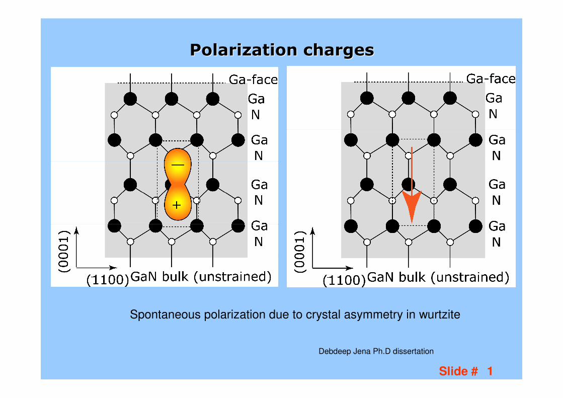
Slide # 1 Polarization charges Polarization charges Spontaneous polarization due to crystal asymmetry in wurtzite Debdeep Jena Ph.D dissertation
Transcript of 16 Polarization and 2D gas - University of South Carolinaee.sc.edu/personal/faculty/simin/ELCT871/16...
Slide # 1
Polarization chargesPolarization charges
Spontaneous polarization due to crystal asymmetry in wurtzite
Debdeep Jena Ph.D dissertation
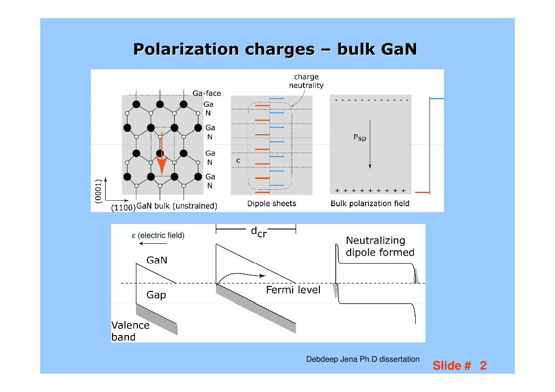
Slide # 2
Polarization charges Polarization charges –– bulk GaNbulk GaN
ε (electric field)
Debdeep Jena Ph.D dissertation
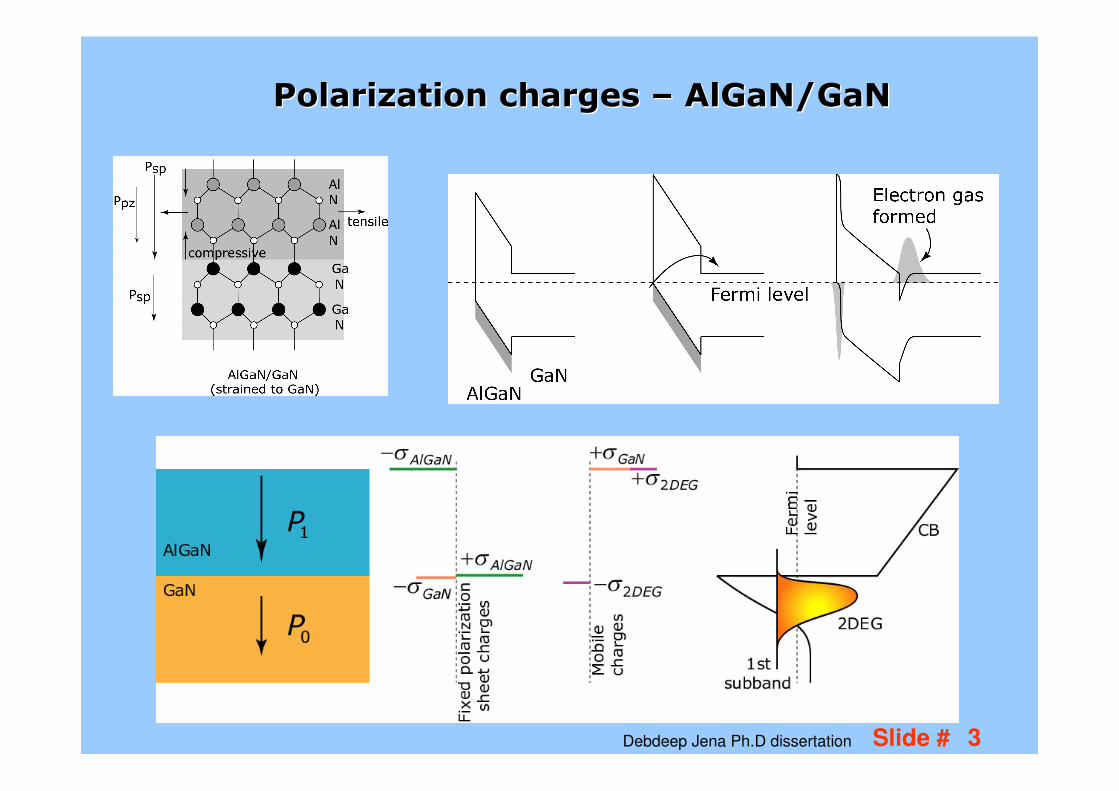
Slide # 3
Polarization charges Polarization charges –– AlGaN/GaNAlGaN/GaN
Debdeep Jena Ph.D dissertation
Slide # 4
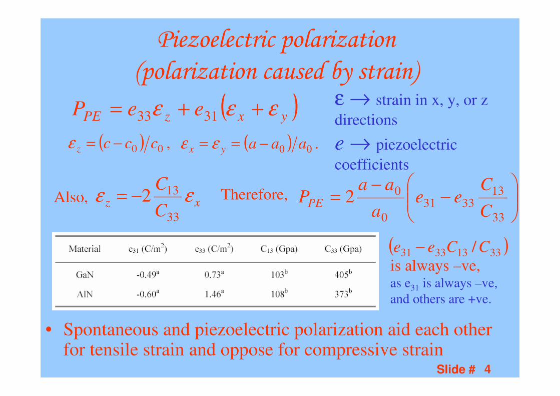
Piezoelectric polarization
(polarization caused by strain)
• Spontaneous and piezoelectric polarization aid each other for tensile strain and oppose for compressive strain
( )yxzPE eeP εεε ++= 3133
( ) ,00 cccz −=ε ( ) .00 aaayx −== εε
xzC
Cεε
33
132−=
−
−=
33
133331
0
02C
Cee
a
aaPPE
( )33133331 / CCee −is always –ve, as e31 is always –ve, and others are +ve.
Also, Therefore,
ε → strain in x, y, or z directions
e → piezoelectric coefficients
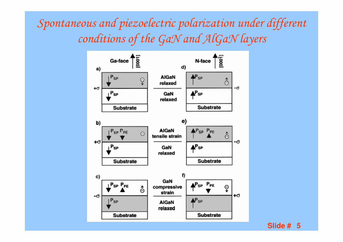
Slide # 5
Spontaneous and piezoelectric polarization under different
conditions of the GaN and AlGaN layers
Slide # 6
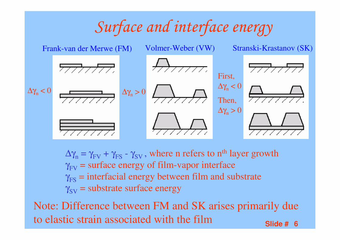
Surface and interface energy
Note: Difference between FM and SK arises primarily due to elastic strain associated with the film
Volmer-Weber (VW)Frank-van der Merwe (FM) Stranski-Krastanov (SK)
∆γn < 0 ∆γn > 0
First, ∆γn < 0
Then, ∆γn > 0
∆γn = γFV + γFS - γSV , where n refers to nth layer growthγFV = surface energy of film-vapor interfaceγFS = interfacial energy between film and substrateγSV = substrate surface energy
Slide # 7
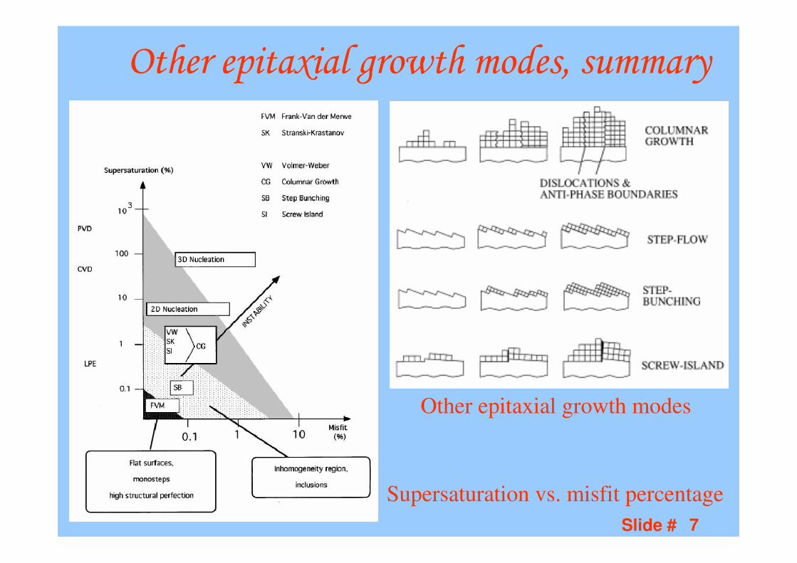
Other epitaxial growth modes, summary
Supersaturation vs. misfit percentage
Other epitaxial growth modes
Slide # 8
Common growth techniques• Bulk crystal growth
– Czochralski: Liquid to solid (Si, GaAs)– Bridgman: Liquid to solid (CdTe, other II-VI compounds)– Sublimation: Vapor to solid (SiC, GaN?)
• Epitaxial crystal growth– Liquid phase epitaxy: substrate moves from one melt to another
(Ex: GaAs)• Adv: Simple, high quality defect free layers, equilibrium growth• Disadv: Multiple layers difficult, QW structure difficult, poor layer interface
– Chemical vapor deposition (Ex: all compound semiconductors, Si)• Adv: Very high quality, high throughput• Disadv: Toxic gases, non-uniform, not as abrupt as MBE
– Molecular beam epitaxy (Ex: all compound semiconductors)• Adv: Very high quality, no toxic gases, very abrupt• Disadv: Low throughput, can be unstable from run to run
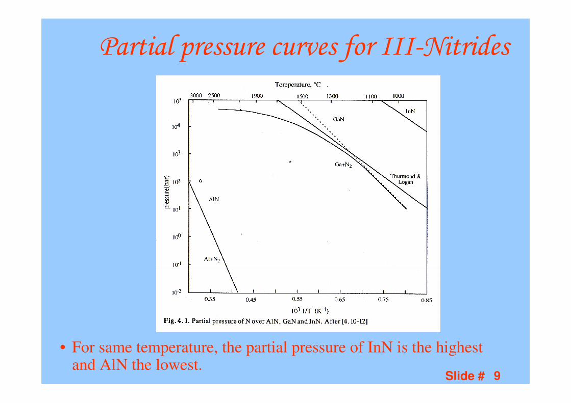
Slide # 9
Partial pressure curves for III-Nitrides
• For same temperature, the partial pressure of InN is the highest and AlN the lowest.
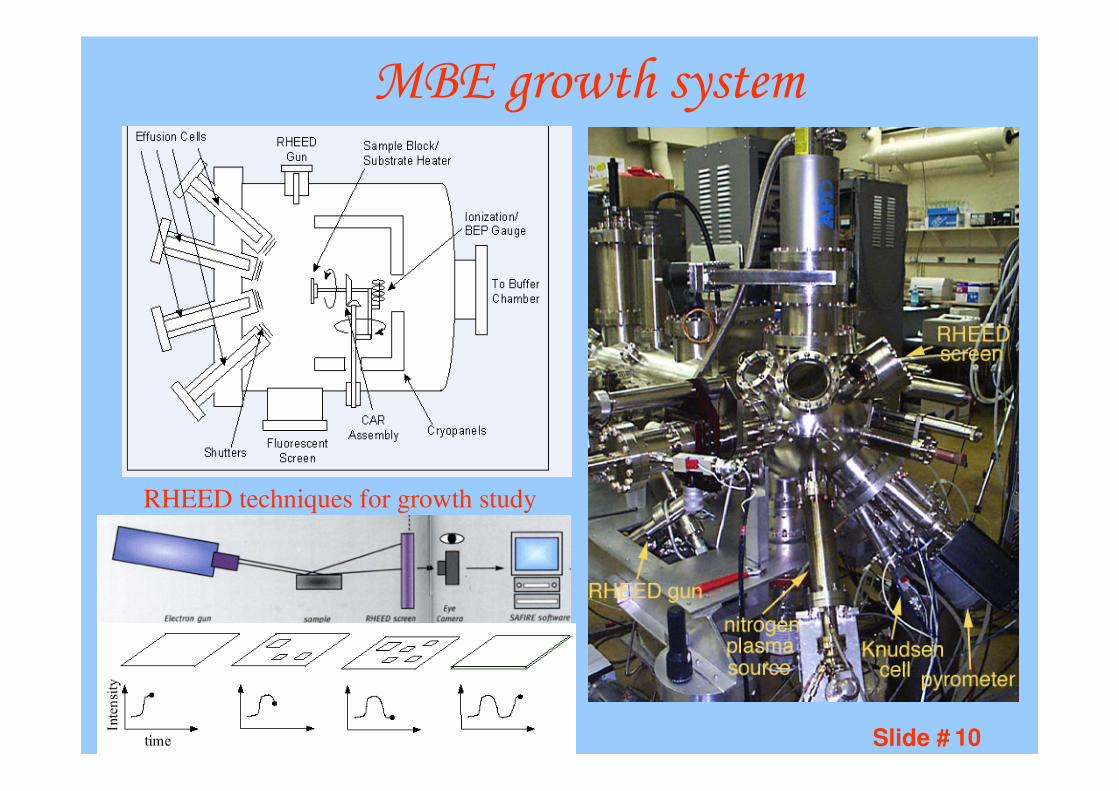
Slide # 10
MBE growth system
RHEED techniques for growth study
Slide # 11
General MBE growth features
• Advantages– Precise layer by layer growth process– Excellent in-situ growth rate monitoring possible– Very abrupt (one atomic layer) growth possible– Can replicate starting layers in excellent manner
• Disadvantages– Growth occurs far from equilibrium and is not
thermodynamically favorable – Growth temperature lower and so film quality is not
as good
– Slower growth rate than MOCVD; difficult design for multiple wafers
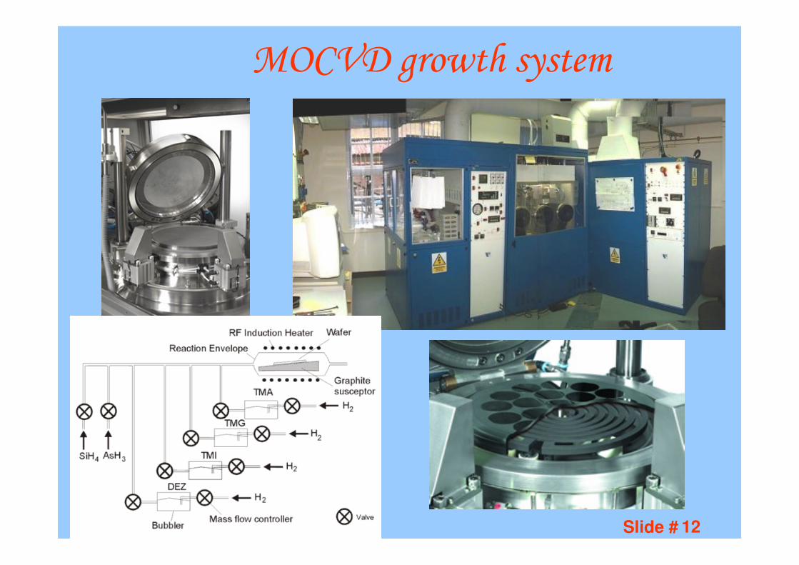
Slide # 12
MOCVD growth system
Slide # 13
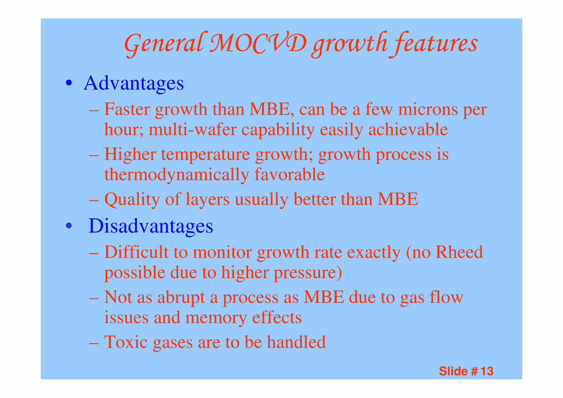
General MOCVD growth features
• Advantages– Faster growth than MBE, can be a few microns per
hour; multi-wafer capability easily achievable– Higher temperature growth; growth process is
thermodynamically favorable– Quality of layers usually better than MBE
• Disadvantages– Difficult to monitor growth rate exactly (no Rheed
possible due to higher pressure)– Not as abrupt a process as MBE due to gas flow
issues and memory effects– Toxic gases are to be handled
Slide # 14
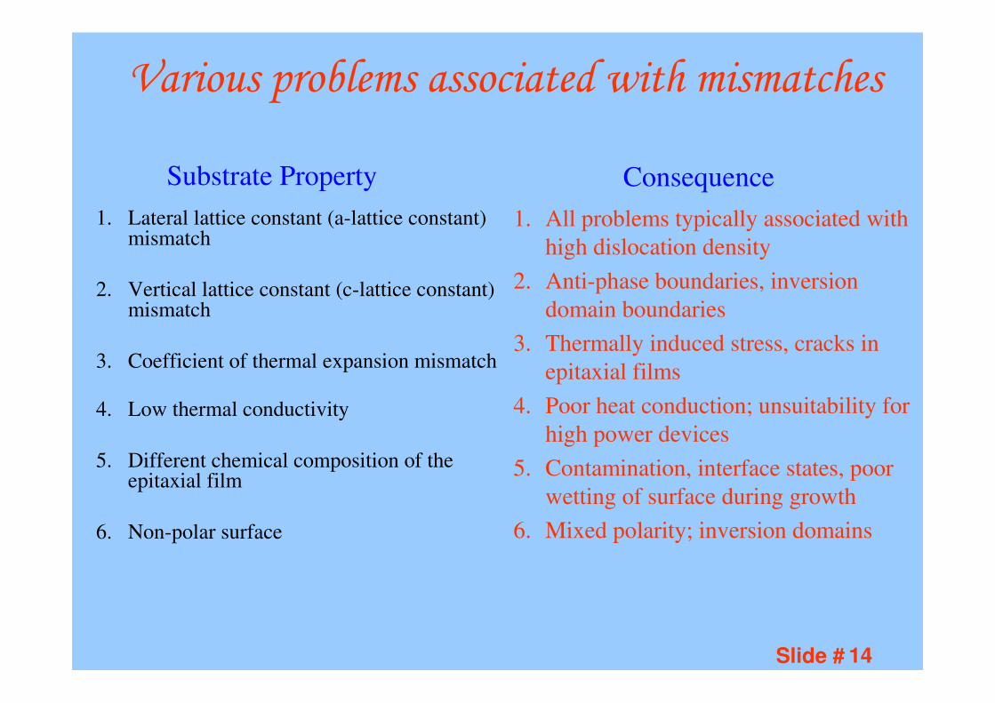
Various problems associated with mismatches
1. Lateral lattice constant (a-lattice constant) mismatch
2. Vertical lattice constant (c-lattice constant) mismatch
3. Coefficient of thermal expansion mismatch
4. Low thermal conductivity
5. Different chemical composition of the epitaxial film
6. Non-polar surface
Substrate Property Consequence1. All problems typically associated with
high dislocation density
2. Anti-phase boundaries, inversion domain boundaries
3. Thermally induced stress, cracks in epitaxial films
4. Poor heat conduction; unsuitability for high power devices
5. Contamination, interface states, poor wetting of surface during growth
6. Mixed polarity; inversion domains
Slide # 15
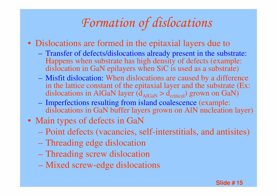
Formation of dislocations
• Dislocations are formed in the epitaxial layers due to– Transfer of defects/dislocations already present in the substrate:
Happens when substrate has high density of defects (example: dislocation in GaN epilayers when SiC is used as a substrate)
– Misfit dislocation: When dislocations are caused by a difference in the lattice constant of the epitaxial layer and the substrate (Ex: dislocations in AlGaN layer (dAlGaN > dcritical) grown on GaN)
– Imperfections resulting from island coalescence (example: dislocations in GaN buffer layers grown on AlN nucleation layer)
• Main types of defects in GaN– Point defects (vacancies, self-interstitials, and antisites)– Threading edge dislocation– Threading screw dislocation– Mixed screw-edge dislocations
Slide # 16
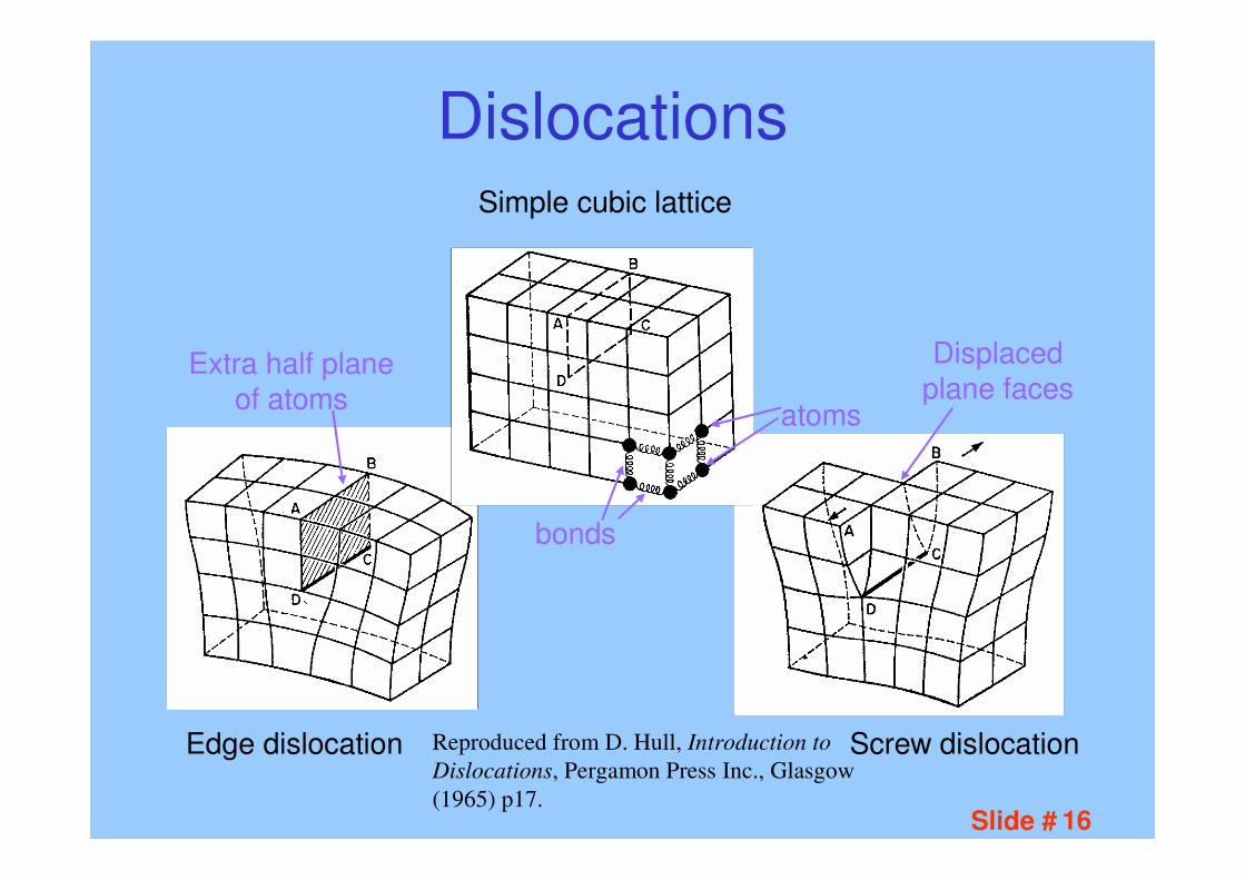
Dislocations
Reproduced from D. Hull, Introduction to
Dislocations, Pergamon Press Inc., Glasgow (1965) p17.
Simple cubic lattice
atoms
bonds
Edge dislocation
Extra half plane of atoms
Screw dislocation
Displaced plane faces
Slide # 17
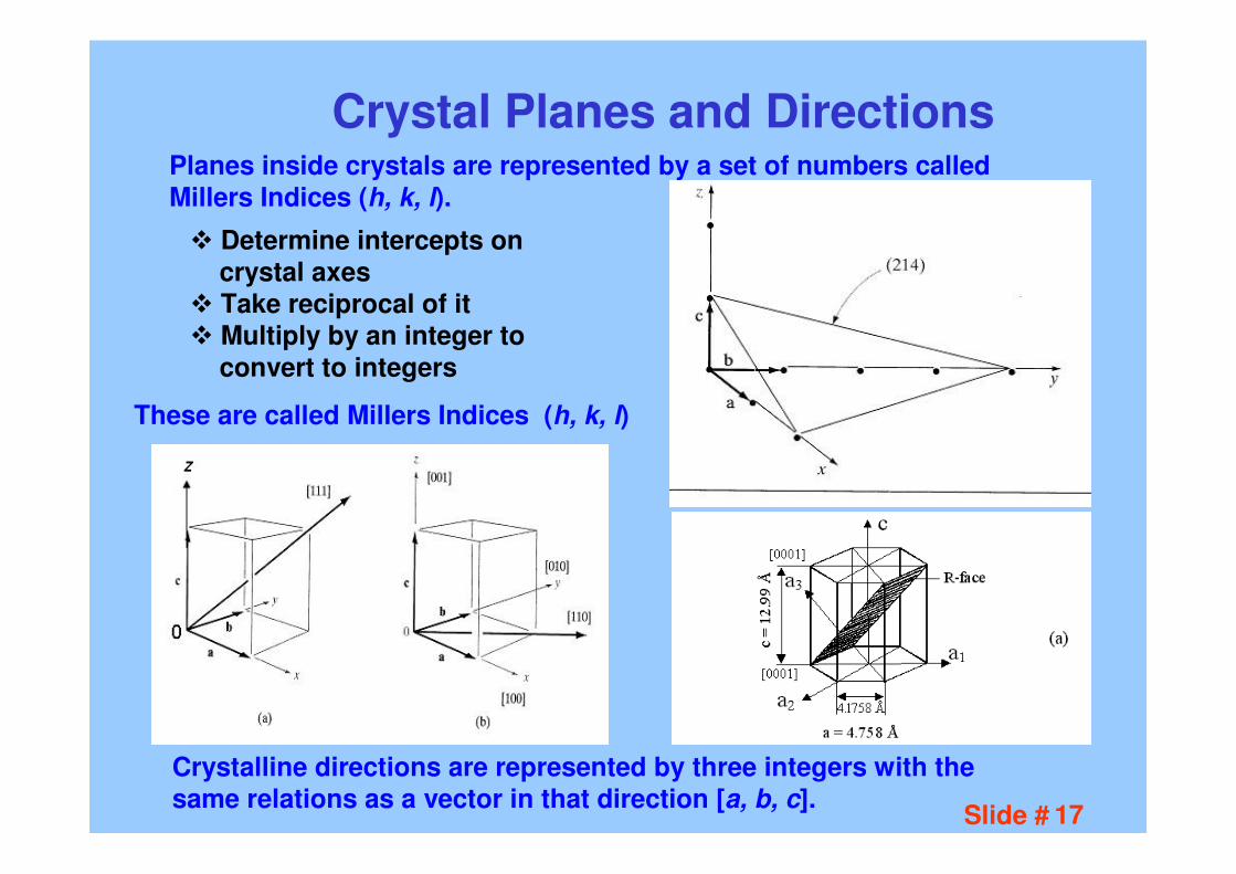
Crystal Planes and DirectionsPlanes inside crystals are represented by a set of numbers called Millers Indices (h, k, l).
Determine intercepts on crystal axes
Take reciprocal of it
Multiply by an integer to
convert to integers
These are called Millers Indices (h, k, l)
Crystalline directions are represented by three integers with the same relations as a vector in that direction [a, b, c].
Slide # 18
Major techniques to reduce dislocations• Bulk growth
– By direct synthesis (from Ga metal and nitrogen)– By sublimation (by using GaN powder as starting material, and
by vapor transport of Ga, which later reacts with NH3)
• Exotic substrates– Si– ZnO– Lithium niobate– Lithium gallate
• Lateral epitaxial overgrowth (LEO) or epitaxial lateral overgrowth (ELO)
• Pendeo-epitaxial growth (pendeo means suspended)• Quasi-bulk growth by HVPE on sapphire
Slide # 19
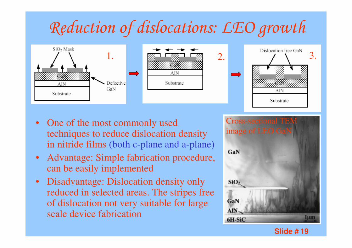
Reduction of dislocations: LEO growth
Cross-sectional TEM image of LEO GaN
1. 2. 3.
• One of the most commonly used techniques to reduce dislocation density in nitride films (both c-plane and a-plane)
• Advantage: Simple fabrication procedure, can be easily implemented
• Disadvantage: Dislocation density only reduced in selected areas. The stripes free of dislocation not very suitable for large scale device fabrication
Slide # 20
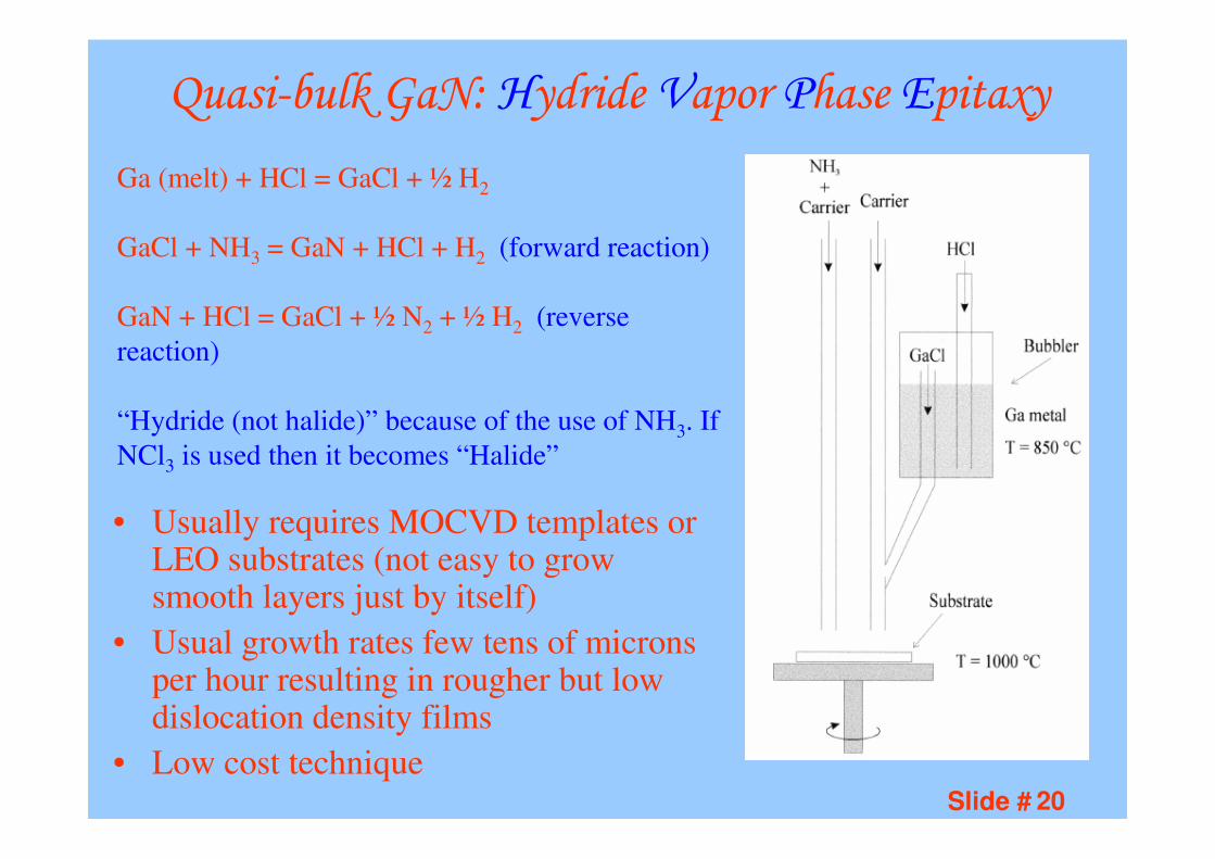
Quasi-bulk GaN: Hydride Vapor Phase Epitaxy
• Usually requires MOCVD templates or LEO substrates (not easy to grow smooth layers just by itself)
• Usual growth rates few tens of microns per hour resulting in rougher but low dislocation density films
• Low cost technique
Ga (melt) + HCl = GaCl + ½ H2
GaCl + NH3 = GaN + HCl + H2 (forward reaction)
GaN + HCl = GaCl + ½ N2 + ½ H2 (reverse reaction)
“Hydride (not halide)” because of the use of NH3. If NCl3 is used then it becomes “Halide”
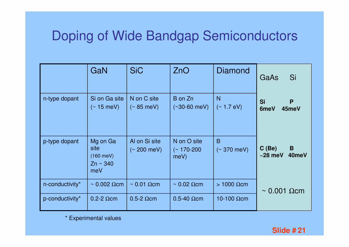
Slide # 21
10-100 Ωcm0.5-40 Ωcm0.5-2 Ωcm0.2-2 Ωcmp-conductivity*
> 1000 Ωcm~ 0.02 Ωcm~ 0.01 Ωcm~ 0.002 Ωcmn-conductivity*
B
(~ 370 meV)
N on O site
(~ 170-200 meV)
Al on Si site
(~ 200 meV)
Mg on Gasite
(160 meV)
Zn ~ 340 meV
p-type dopant
N
(~ 1.7 eV)
B on Zn
(~30-60 meV)
N on C site
(~ 85 meV)
Si on Ga site
(~ 15 meV)
n-type dopant
DiamondZnOSiCGaNGaAs Si
Si P6meV 45meV
C (Be) B~28 meV 40meV
~ 0.001 Ωcm
* Experimental values
Doping of Wide Bandgap Semiconductors
Slide # 22
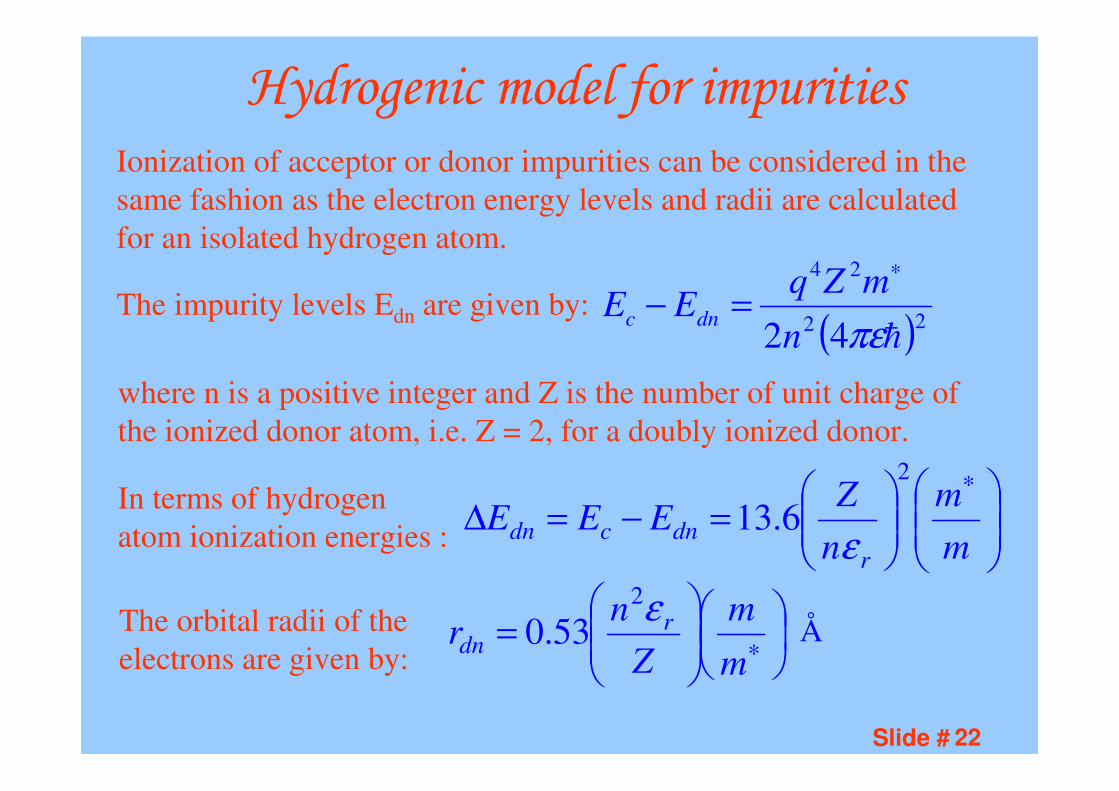
Hydrogenic model for impuritiesIonization of acceptor or donor impurities can be considered in the same fashion as the electron energy levels and radii are calculated for an isolated hydrogen atom.
( )22
24
42 πεn
mZqEE dnc
∗
=−The impurity levels Edn are given by:
where n is a positive integer and Z is the number of unit charge of the ionized donor atom, i.e. Z = 2, for a doubly ionized donor.
In terms of hydrogen atom ionization energies :
=−=∆
∗
m
m
n
ZEEE
r
dncdn
2
6.13ε
=
∗m
m
Z
nr rdn
ε2
53.0 ÅThe orbital radii of the electrons are given by:
Slide # 23
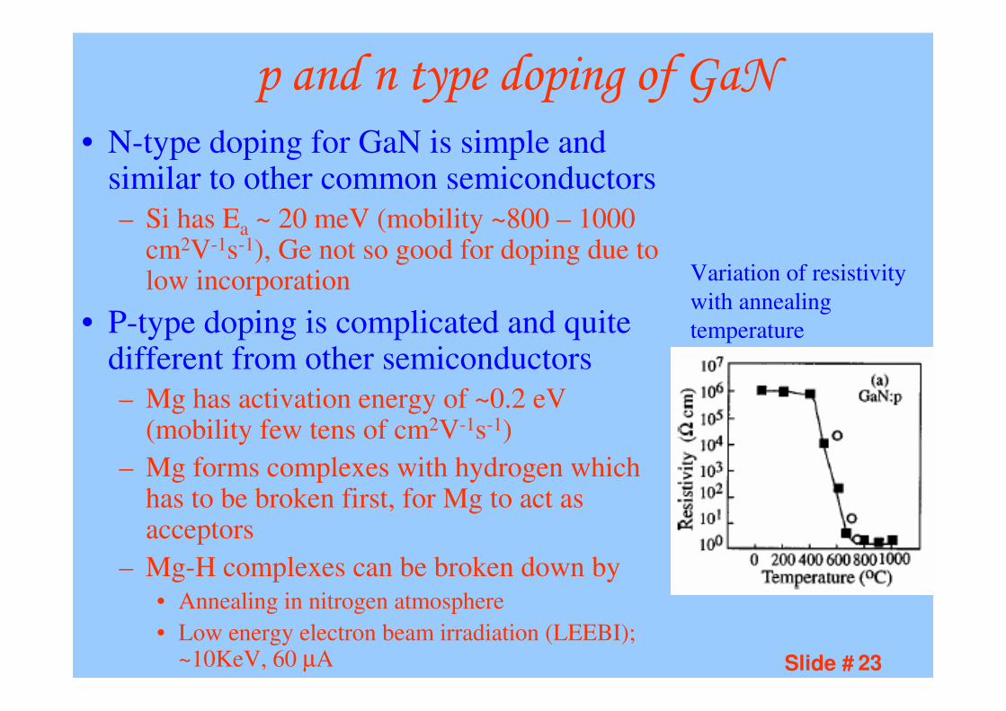
p and n type doping of GaN
• N-type doping for GaN is simple and similar to other common semiconductors– Si has Ea ~ 20 meV (mobility ~800 – 1000
cm2V-1s-1), Ge not so good for doping due to low incorporation
• P-type doping is complicated and quite different from other semiconductors– Mg has activation energy of ~0.2 eV
(mobility few tens of cm2V-1s-1)– Mg forms complexes with hydrogen which
has to be broken first, for Mg to act as acceptors
– Mg-H complexes can be broken down by • Annealing in nitrogen atmosphere• Low energy electron beam irradiation (LEEBI);
~10KeV, 60 µA
Variation of resistivitywith annealing temperature
Slide # 24
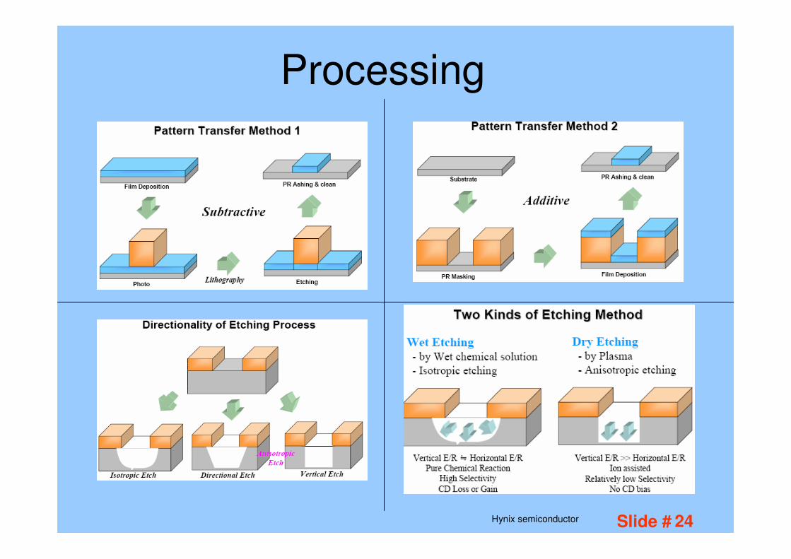
Processing
Hynix semiconductor
Slide # 25
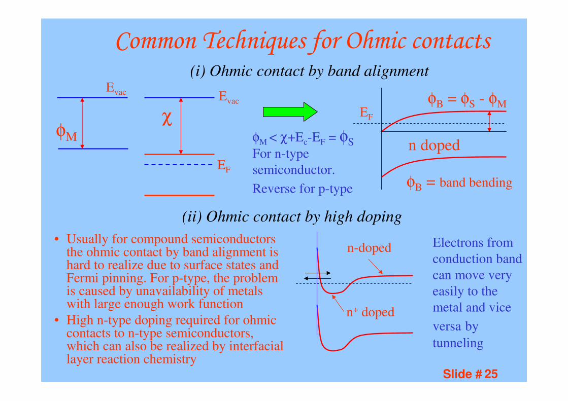
Common Techniques for Ohmic contacts
• Usually for compound semiconductors the ohmic contact by band alignment is hard to realize due to surface states and Fermi pinning. For p-type, the problem is caused by unavailability of metals with large enough work function
• High n-type doping required for ohmiccontacts to n-type semiconductors, which can also be realized by interfacial layer reaction chemistry
φM
Evac Evac
χ
EF
φM < χ+Ec-EF = φSFor n-type semiconductor. Reverse for p-type
(ii) Ohmic contact by high doping
Electrons from conduction band can move very easily to the metal and vice versa by tunneling
n+ doped
(i) Ohmic contact by band alignment
n doped
φB = φS - φMEF
φB = band bending
n-doped
Slide # 26
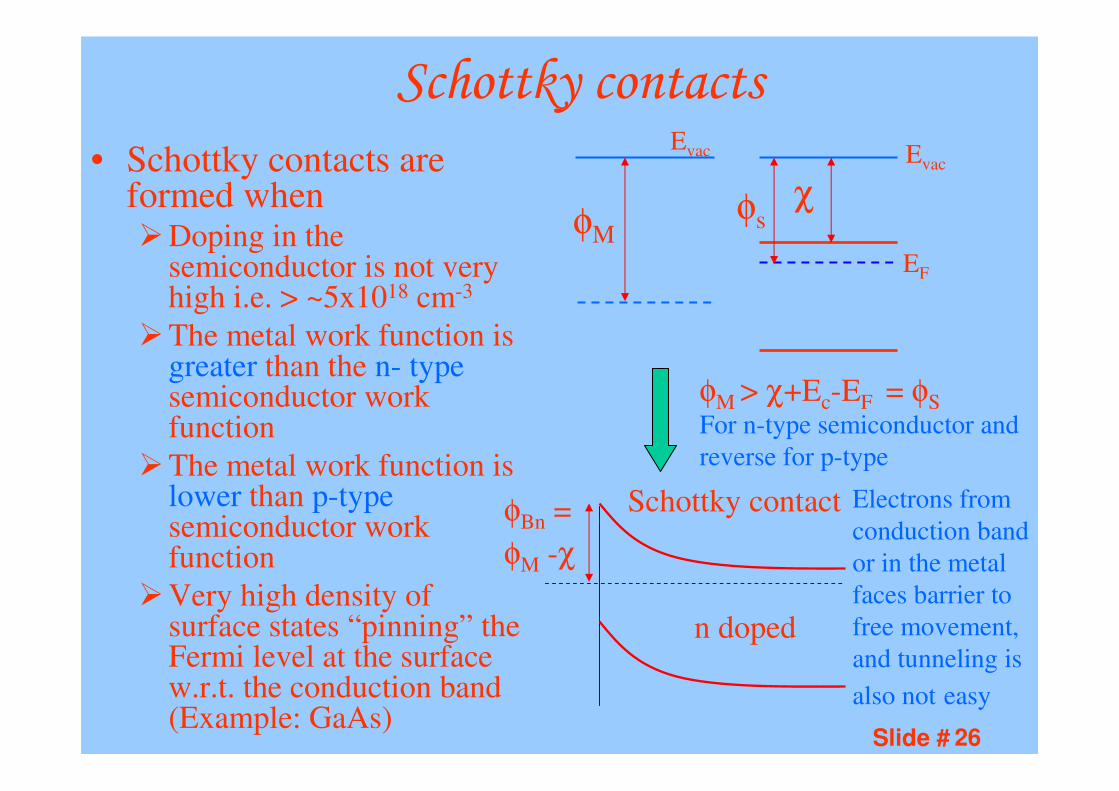
Schottky contacts
• Schottky contacts are formed whenDoping in the
semiconductor is not very high i.e. > ~5x1018 cm-3
The metal work function is greater than the n- typesemiconductor work function
The metal work function is lower than p-typesemiconductor work function
Very high density of surface states “pinning” the Fermi level at the surface w.r.t. the conduction band (Example: GaAs)
Schottky contact
n doped
Electrons from conduction band or in the metal faces barrier to free movement, and tunneling is also not easy
φM
Evac Evac
χ
EF
φM > χ+Ec-EF = φS For n-type semiconductor and reverse for p-type
φs
φBn = φM -χ
Slide # 27
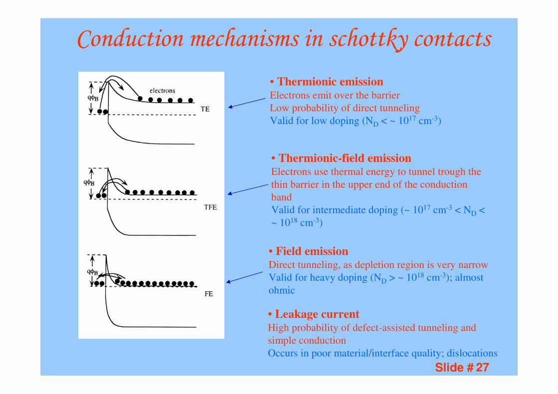
Conduction mechanisms in schottky contacts
• Thermionic emissionElectrons emit over the barrier Low probability of direct tunnelingValid for low doping (ND < ~ 1017 cm-3)
• Thermionic-field emissionElectrons use thermal energy to tunnel trough the thin barrier in the upper end of the conduction bandValid for intermediate doping (~ 1017 cm-3 < ND < ~ 1018 cm-3)
• Field emissionDirect tunneling, as depletion region is very narrowValid for heavy doping (ND > ~ 1018 cm-3); almost ohmic
• Leakage currentHigh probability of defect-assisted tunneling and simple conductionOccurs in poor material/interface quality; dislocations
Slide # 28
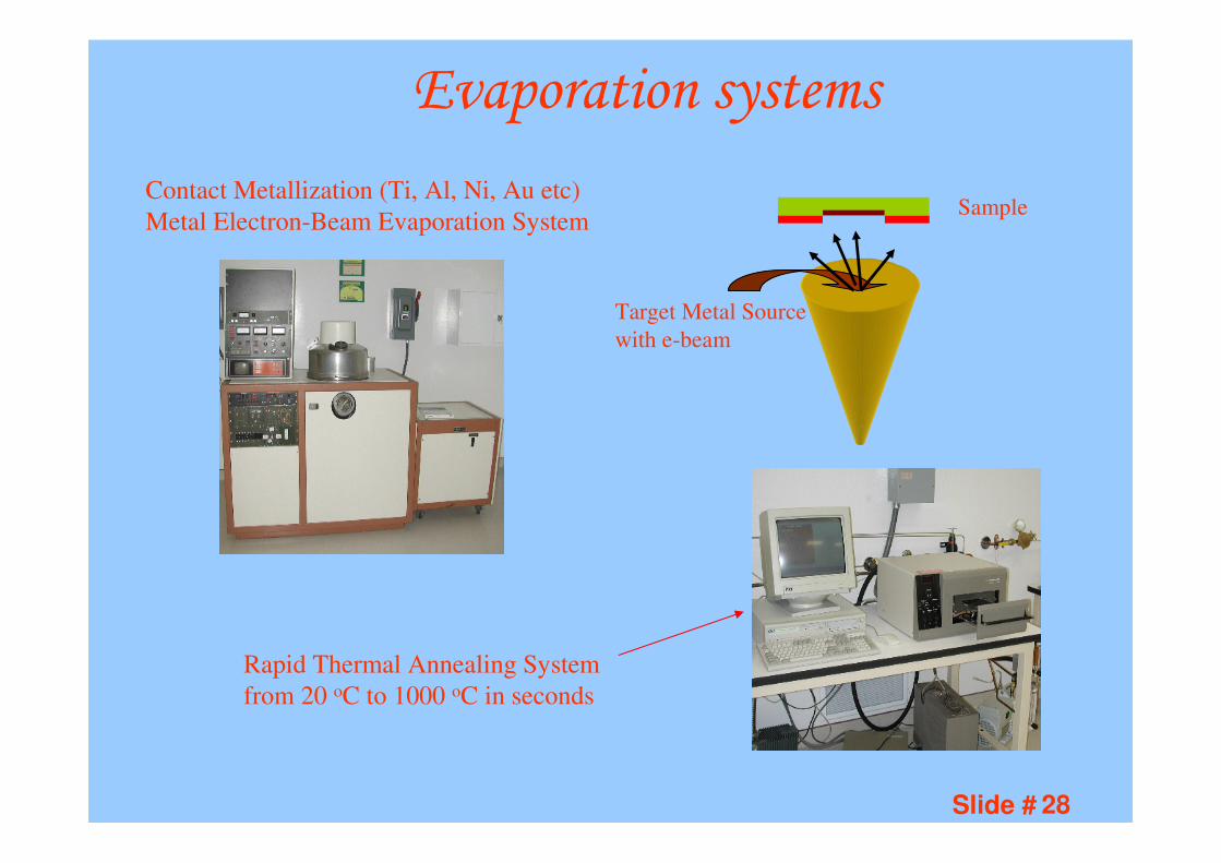
Evaporation systems
Contact Metallization (Ti, Al, Ni, Au etc)Metal Electron-Beam Evaporation System
Rapid Thermal Annealing Systemfrom 20 oC to 1000 oC in seconds
Target Metal Sourcewith e-beam
Sample
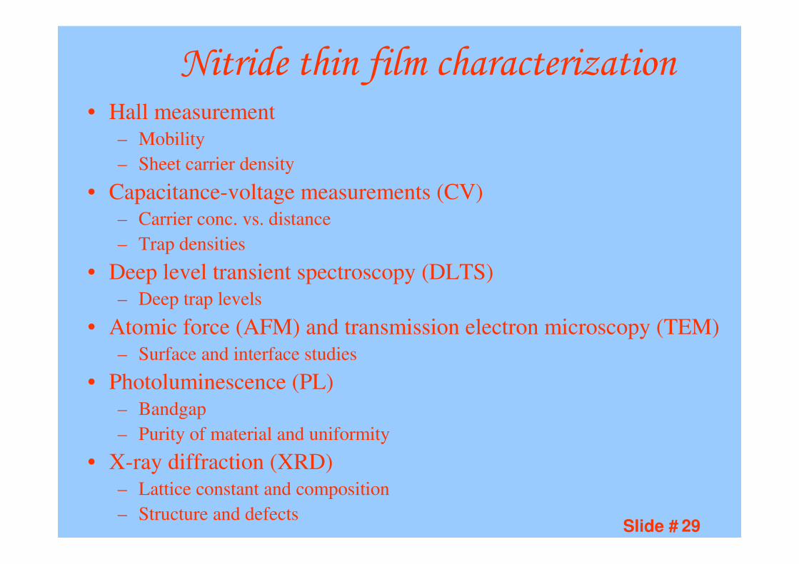
Slide # 29
Nitride thin film characterization• Hall measurement
– Mobility– Sheet carrier density
• Capacitance-voltage measurements (CV)– Carrier conc. vs. distance– Trap densities
• Deep level transient spectroscopy (DLTS)– Deep trap levels
• Atomic force (AFM) and transmission electron microscopy (TEM)– Surface and interface studies
• Photoluminescence (PL)– Bandgap– Purity of material and uniformity
• X-ray diffraction (XRD)– Lattice constant and composition– Structure and defects

Slide # 30
Homework DiscussionHomework DiscussionHomework DiscussionHomework Discussion